Embed Size (px)
Citation preview
Vortex86EX32-Bit x86 Micro Processor
Vortex86EX datasheet Rev 1.3 Page 1Copyright © 2013 DMP
Vortex86EX
Fact Sheet32-BIT x86 MICRO PROCESSOR

Vortex86EX32-Bit x86 Micro Processor
Vortex86EX datasheet Rev 1.3 Page 2Copyright © 2013 DMP
Revision History
Rev. Date History
REV 1.0 2012/10/08 1. Init Draft version.
REV 1.1 2012/12/12
1. Add HW JTAG register1 bit27-29, Flash FFFBCh
bit3-5, NB 64h bit27-29 description.
2. Boot mode update.
3. PCIE target register update.
4. Add Ball Map in 4.1 and PIN Out Table in 4.2
5. Update pin list, signal description.
6. Add Flash FFFBCh bit3-5, NB 64h bit27-29 description.
7. Boot mode update.
8. Add PCI-E target.
9. Add Functions Block Diagram in 3.2 and move System
Block Diagram from 3.2 to 3.1
REV 1.2 2013/04/30
1. Modify the acronym of Secondary ATA Timing Register in
13.5.27.
2. Modify the description of Pin TXN, TXP, RXN and RXP in 4.4
Signal Description.
3. Remove”3.3V power supply” from Features in 14.2 Fast
Ethernet control unit.
4. Modify the value of UART Baud Rate to “57600” in TABLE
Baud Rates, Divisors and 1.8432MHzCrystals in 11.3.12.
Serial Port Register Definition.
5. Add the DDR Timing information in 22.2 DDRIII Interface.
6. Modify the Description of 05h – 04h PMDC, MSAC, IOSAC
in 14.4.
7. Modify the “External 10/100M PHY” to ”RJ45 LAN Port” in
3.2 Functions Block Diagram.
REV 1.3 2013/05/25
1. Modify the minimun of RTC_VDD33 from 2.0 to 2.45 in 21.3
Recommanded DC Operating Conditions.
2. Add the reference information about VPF in 10.7.2
Power-Down/Power-UpConsiderations.
3. Modify the ball name of H1 and H2 in Chap. 4. PIN Function
List.
4. Remove the 08h-0Dh of SPI Control Registers from 7.3.14
SPI Control Registers.
5. Modify the reset value of Interrupt Pin from 03h to 02h in
21.3.2. Full-Duplex SPI Configuration Space Register.

Vortex86EX32-Bit x86 Micro Processor
Vortex86EX datasheet Rev 1.3 Page 3Copyright © 2013 DMP
6. Add Pin Pull-up / Pull-down Description in 4.6.
7. Add the information in 4.5 PIN Capacitance Description.
8. Modify the capacity of SATA from 1.5G to 3.0G, add “up to
the fast speed” in I2C bus and correct I/O Voltage 1.8 ± 10
% to 1.8V± 5 % in chap.2. Features.
9. Modify bit 7& bit 5 of SD Control Register to Reserved.
10. Add Control Register 4 in 7.1.5. Control Registers.
11. The IDSEL in PCI-E Configuration Space Registers is in
AD12/Device1/F[0].
12. Turn M3 & N3 to NC Pin in Chap. 4.
13. Modify the description of bit 2(AICS) of BA+01h (ADC
Control Register).
14. Modify the Function Diagram.
15. Add the information in bit 0 (RST) of 0x00h (Global Control
Register) in 18.6. List of CAN Memory Register.
16. Modify the description of PreScale1 of I2C0 Clock
Frequency Control1 in 11.3.20. I2C Registers.
17. Modify bit 0 of PMBASE+20h, 24h & 28h and bit 5 of 2C &
30h to Reserved bits in 11.3.28. ACPI Register.
18. Fill in the blanks of Max Power and Typical Power in 21.1
Performance and the blank of 21.5 Temperature.
19. Modify ROMCS# to GPCS# in 22.3 ISA Bus Interface.
20. Take off FRAME# from the figures of System Reset.
REV 1.4 2013/06/11
1. Remove information I2C1 .from SB F[0] Internal I2C Control
Register (D7h-D4h).
2, Modify M3 & N3 to AVDD_PERX12 and AVSS_PERX12.
3, Correct page 31, SATA Power, PIN L13 to PIN L3, PIN L14
To PIN L4
4, Correct page 34, 1.2V Power, PIN R5 to PIN P5
DMP reserves the right to make changes without further notice to any products or data
herein to improve reliability, function, or design. Information furnished by DMP is believed to
be accurate and reliable. However, DMP does not assure any liability arising out of the
application or use of this information, nor the application or use of any product or circuit
described herein, neither does it convey any license under its patent rights nor the rights of
others.
Copyright © 2013 DMP Electronics INC. All rights reserved.
Vortex86EX32-Bit x86 Micro Processor
Vortex86EX datasheet Rev 1.3 Page 4Copyright © 2013 DMP
CONTENTS1. Overview ........................................................................................................................................ 92. Features ......................................................................................................................................... 93. Block Diagram............................................................................................................................. 11
3.1 System Block Diagram .............................................................................................. 113.2 Functions Block Diagram........................................................................................... 123.3 PCI Device List .......................................................................................................... 13
4. PIN Function List......................................................................................................................... 144.1 BGA Ball Map ............................................................................................................ 144.2 PIN Out Table ............................................................................................................ 174.3 Pin List Table ............................................................................................................. 204.4 Signal Description...................................................................................................... 224.5 PIN Capacitance Description..................................................................................... 334.6 PIN Pull-up / Pull-down Description .......................................................................... 334.7 The Registers only reset by power-good................................................................... 40
5. System Address Map.................................................................................................................. 415.1 Memory Address Ranges .......................................................................................... 41
5.1.1 Dos Compatibility Region ................................................................................................. 425.1.2 Extended Memory Region ................................................................................................ 43
5.2 Memory Shadowing................................................................................................... 445.3 I / O Address Space................................................................................................... 44
6. Operation Mode........................................................................................................................... 457. Register Sets ............................................................................................................................... 46
7.1 Core Registers........................................................................................................... 467.1.1 General-Purpose Registers (Detail information in Chap.11.1.1) ....................................... 467.1.2 Segment Registers (Detail information in Chap.11.1.2) .................................................... 467.1.3 Instruction Pointer (Detail information in Chap.11.1.3)...................................................... 477.1.4 Flags Register (Detail information in Chap.11.1.4) ........................................................... 477.1.5 Control Registers (Detail information in Chap.11.1.5)....................................................... 477.1.6 System Address Registers (Detail information in Chap.11.1.6) ........................................ 477.1.7 FPU Registers (Detail information in Chap.11.1.7) ........................................................... 47
7.2 CPU MSR Registers.................................................................................................. 487.2.1 MSR Registers (Detail information in Chap.11.2) ............................................................. 48
7.3 I / O Mapped Registers.............................................................................................. 497.3.1 PCI Configuration Registers (Detail information in Chap.11.3.1) ...................................... 497.3.2 Slave DMA Controller Registers(Detail information in Chap.11.3.2) ................................. 497.3.3 DMA Page Registers (Detail information in Chap.11.3.3) ................................................. 507.3.4 Master DMA Controller Registers (Detail information in Chap.11.3.4) .............................. 507.3.5 DMA High Page Registers (Detail information in Chap.11.3.5)......................................... 517.3.6 Timer / Counter Registers (Detail information in Chap.11.3.6).......................................... 517.3.7 Indirect Access Registers (Detail information in Chap.11.3.7) .......................................... 517.3.8 Master Interrupt Controller Registers (Detail information in Chap.11.3.8)......................... 517.3.9 Slave Interrupt Controller Registers (Detail information in Chap.11.3.9)........................... 517.3.10 Interrupt Edge / Level Control Registers (Detail information in Chap.11.3.10).................. 527.3.11 Keyboard / Mouse Control Registers(Detail information in Chap.11.3.11) ........................ 527.3.12 Serial Port Registers (Detail information in Chap.11.3.12)................................................ 527.3.13 Parallel Port Registers (Detail information in Chap.11.3.13)............................................. 547.3.14 SPI Control Registers (Detail information in Chap.11.3.14) .............................................. 547.3.15 GPIO Registers (Detail information in Chap.11.3.15) ....................................................... 557.3.16 NMI Status and Control Register (Detail information in Chap.11.3.16) ............................. 567.3.17 WDT Registers (Detail information in Chap.11.3.17) ........................................................ 567.3.18 CMOS Memory & RTC Registers (Detail information in Chap.11.3.18) ............................ 577.3.19 System Control Register(Detail information in Chap.11.3.19)........................................... 577.3.20 I2C Registers(Detail information in Chap.11.3.20)............................................................ 577.3.21 DOS 4Gpage Access Registers(Detail information in Chap.11.3.21)................................ 587.3.22 Spare Registers(Detail information in Chap.11.3.22)........................................................ 587.3.23 SMM Registers(Detail information in Chap.11.3.23)......................................................... 587.3.24 Fast Ethernet MAC Registers(Detail information in Chap.14.7)........................................ 597.3.25 USB 1.1 OHCI Operation Registers(Detail information in Chap.12.3.2) ........................... 617.3.26 USB 2.0 EHCI Operation Registers(Detail information in Chap.12.3.4) ........................... 627.3.27 USB Device Operation Registers(Detail information in Chap.15.4) .................................. 63
Vortex86EX32-Bit x86 Micro Processor
Vortex86EX datasheet Rev 1.3 Page 5Copyright © 2013 DMP
7.3.28 SD/SATA Controller Registers(Detail information in Chap.13.7) ....................................... 647.3.29 HDA Controller Registers(Detail information in Chap.16.4) .............................................. 657.3.30 ADC Registers(Detail information in Chap.11.3.24).......................................................... 667.3.31 ACPI Registers (Detail information in Chap.11.3.25)........................................................ 667.3.32 CrossBar Config Registers (Detail information in Chap.11.3.26) ...................................... 67
7.4 Configuration Space Registers.................................................................................. 727.4.1 NB Function 0 Configuration Space Registers (IDSEL = AD11/Device 0) (Detail
information in Chap.11.3.1)............................................................................................... 737.4.2 NB Function 1 Configuration Registers (IDSEL = AD11/Device0/Function1) (Detail
information in Chap.11.3.2)............................................................................................... 747.4.3 SB Configuration Space Registers (IDSEL = AD18/Device 7/Function 1) (Detail
information in Chap.11.3.4)............................................................................................... 757.4.4 MAC PCI Configuration Space Registers (IDSEL = AD19/Device 8) (Detail information in
Chap.14.4)........................................................................................................................ 767.4.5 USB1.1 Configuration Space Registers (IDSEL = AD21/Device10/Function0(Detail
information in Chap.12.3.1) .............................................................................................. 767.4.6 USB2.0 Configuration Space Registers (IDSEL = AD21/Device10/Function1) (Detail
information in Chap.12.3.3) .............................................................................................. 777.4.7 USB Device PCI Configuration Registers Definition ((IDSEL = AD26/Device15/Function0)
(Detail information in Chap.15.3) ...................................................................................... 787.4.8 SD/SATA Configuration Space Registers (IDSEL = AD23/Device12/Function0) (Detail
information in Chap.13.5) ................................................................................................. 797.4.9 HDA Configuration Space Registers (IDSEL = AD25/Device14/Function0) (Detail
information in Chap.16.3) ................................................................................................. 807.4.10 PCI-E Configuration Space Registers (IDSEL = AD12/Device1/Function0) (Detail
information in Chap.12.3) ................................................................................................. 817.4.11 Motion Controller Configuration Space Registers (IDSEL = AD27/Device16/Function0)
(Detail information in Chap.20.3.1) ................................................................................... 827.4.12 PCIe Target Configuration Space Registers (Detail information in Chap.19.1) ................. 837.4.13 Duplex SPI Configuration Space Registers (IDSEL = AD27/Device16/Function1) (Detail
information in Chap.20.3.2) .............................................................................................. 848. Instruction Set ............................................................................................................................. 859. Addressing Modes...................................................................................................................... 86
9.1 Register and Immediate Modes ................................................................................ 869.2 32-Bit Memory Addressing Modes ............................................................................ 869.3 Differences between 16- and 32-bit Addresses......................................................... 88
10.Functional Description ............................................................................................................... 8910.1 SoC Core................................................................................................................... 8910.2 L1 Cache ................................................................................................................... 9110.3 L2 Cache ................................................................................................................... 9210.4 DDR3 Controller ........................................................................................................ 9210.5 DMA Controller .......................................................................................................... 93
10.5.1 DMA Transfer Modes........................................................................................................ 9410.5.2 DMA Transfer Types ......................................................................................................... 9510.5.3 DMA Timings .................................................................................................................... 9610.5.4 DREQ and DACK# Latency Control ................................................................................. 9610.5.5 Channel Priority ................................................................................................................ 9610.5.6 Register Functionality ....................................................................................................... 9710.5.7 Address Compatibility Mode ............................................................................................. 9710.5.8 Summary of DMA Transfer Sizes...................................................................................... 97
10.5.9 Address Shifting When Programmed for 16-Bit I/O Count by Words ...................... 9810.5.10 Autoinitialize ..................................................................................................................... 9810.5.11 Software Commands ........................................................................................................ 98
10.6 Watchdog Timer....................................................................................................... 10010.6.1 Set the watchdog timer function ..................................................................................... 10010.6.2 Set the watchdog timer Counter ..................................................................................... 10010.6.3 Read the watchdog timer counter value ......................................................................... 10110.6.4 Clear the watchdog timer counter................................................................................... 101
10.7 Real Time Clock ...................................................................................................... 10210.7.1 Clock Accuracy ............................................................................................................... 10210.7.2 Power-Down/Power-UpConsiderations .......................................................................... 10210.7.3 Time, Calendar, and Alarm Locations............................................................................. 10210.7.4 Control Registers............................................................................................................ 10610.7.5 SRAM............................................................................................................................. 109
Vortex86EX32-Bit x86 Micro Processor
Vortex86EX datasheet Rev 1.3 Page 6Copyright © 2013 DMP
10.7.6 Interrupts ........................................................................................................................ 10910.7.7 Oscillator Control Bits ..................................................................................................... 11010.7.8 Periodic Interrupt Selection............................................................................................. 11010.7.9 Update Cycle ...................................................................................................................111
10.8 ProgrammableTimer................................................................................................ 11210.8.1 Programming the Interval Timer ..................................................................................... 113
10.9 Programmable Interrupt Controller.......................................................................... 11710.9.1 Programming the Interrupt Controller ............................................................................. 11710.9.2 End-of-Interrupt Operation.............................................................................................. 11910.9.3 Modes of Operation ........................................................................................................ 12010.9.4 Cascade Mode ............................................................................................................... 12110.9.5 Edge- and Level-Triggered Mode ................................................................................... 12210.9.6 Interrupt Masks............................................................................................................... 12210.9.7 Reading the Interrupt Controller Status .......................................................................... 12310.9.8 Interrupt Steering............................................................................................................ 124
10.10 KeyBoard Controller ................................................................................................ 12410.10.1 Host Interface ................................................................................................................. 12610.10.2 Data Registers and Status Register................................................................................ 12610.10.3 Keyboard and Mouse Interface....................................................................................... 12710.10.4 KIRQ and MlRQ.............................................................................................................. 12710.10.5 A20M_ Setting ................................................................................................................ 127
10.11 PARALLEL PORT.................................................................................................... 12910.11.1 IBM XT/AT COMPATIBLE, BI-DIRECTIONAL AND EPP MODES.................................. 13110.11.2 EXTENDED CAPABILITIES PARALLEL PORT.............................................................. 14510.11.3 ISA IMPLEMENTATION STANDARD ............................................................................. 14610.11.4 OPERATION................................................................................................................... 15610.11.5 DMA TRANSFERS ......................................................................................................... 158
10.12 FIFO UART.............................................................................................................. 16110.12.1 Transmit Operation ......................................................................................................... 16110.12.2 Receive Operation.......................................................................................................... 16210.12.3 MODEM Control Lines.................................................................................................... 16210.12.4 FIFO Interrupt Mode Operation ...................................................................................... 16210.12.5 FIFO Polled Mode Operation.......................................................................................... 16410.12.6 Timing Waveforms.......................................................................................................... 164
10.13 GPIO Interface......................................................................................................... 16510.14 DOS 4Gpage Access............................................................................................... 16510.15 Flash Strap .............................................................................................................. 167
10.15.1 Flash Strap Region Summary. ........................................................................................ 16710.15.2 CrossBar Config ............................................................................................................. 16710.15.3 Ethernet MAC Address ................................................................................................... 16810.15.4 PLL Config & Others....................................................................................................... 16910.15.5 Customer Data ............................................................................................................... 169
11. Register Description................................................................................................................. 17011.1 Core Registers......................................................................................................... 170
11.1.1 General-Purpose Registers ............................................................................................ 17011.1.2 Segment Registers ......................................................................................................... 17311.1.3 Instruction Pointer Register ............................................................................................ 17611.1.4 Flags Register ................................................................................................................ 17611.1.5 Control Registers............................................................................................................ 18011.1.6 System Address Registers ............................................................................................. 18511.1.7 FPU Registers ................................................................................................................ 188
11.2 CPU MSR Registers................................................................................................ 19811.3 I / O Mapped Registers............................................................................................ 202
11.3.1 PCI Configuration Registers ........................................................................................... 20211.3.2 Slave DMA Control Registers ......................................................................................... 20311.3.3 DMA Pager Registers ..................................................................................................... 21311.3.4 Master DMA Control Registers ....................................................................................... 21611.3.5 DMA High Page Registers.............................................................................................. 22411.3.6 Timer / Counter Registers............................................................................................... 22611.3.7 Indirect Access Registers ............................................................................................... 229
11.3.8 Indirect Access Registers for WDT0...................................................................... 22911.3.9 Indirect Access Registers for GPIO P0/P1............................................................ 23211.3.10 Indirect Access Registers for Lock / Unlock .......................................................... 233
11.3.11 Master Interrupt Control Registers.................................................................................. 234
Vortex86EX32-Bit x86 Micro Processor
Vortex86EX datasheet Rev 1.3 Page 7Copyright © 2013 DMP
11.3.12 Slave Interrupt Control Registers.................................................................................... 23511.3.13 Interrupt Edge / Level Control Registers......................................................................... 23611.3.14 Keyboard / Mouse Control Registers.............................................................................. 23811.3.15 Serial Port Registers....................................................................................................... 23911.3.16 Parallel Port Register...................................................................................................... 25611.3.17 SPI Control Registers ..................................................................................................... 25711.3.18 GPIO Registers .............................................................................................................. 26011.3.19 NMI Status and Control Register .................................................................................... 27411.3.20 WDT Registers ............................................................................................................... 27511.3.21 CMOS Memory & RTC Registers ................................................................................... 27811.3.22 System Function Register .............................................................................................. 27911.3.23 I2C Registers.................................................................................................................. 27911.3.24 DOS 4Gpage Access...................................................................................................... 28411.3.25 Spare Registers .............................................................................................................. 28611.3.26 SMM Registers............................................................................................................... 29111.3.27 ADC Registers................................................................................................................ 29311.3.28 ACPI Registers............................................................................................................... 29611.3.29 CrossBar Config Registers ............................................................................................. 304
11.4 PCI Configuration Space Registers (by request) .................................................... 31411.4.1 North Bridge Function 0 Configuration Registers ........................................................... 31411.4.2 North Bridge Function 1 Configuration Registers ........................................................... 33811.4.3 South Bridge Function 0 Configuration Registers........................................................... 36111.4.4 South Bridge Function 1 Configuration Registers........................................................... 390
12.USB2.0 Host Controller ............................................................................................................ 39912.1 Features .................................................................................................................. 399
12.1.1 USB1.1 Host Controller .................................................................................................. 39912.1.2 USB2.0 Host Controller .................................................................................................. 399
12.2 General Descriptions ............................................................................................... 40012.3 Register Definition ................................................................................................... 400
12.3.1 USB1.1 Configuration Space Register............................................................................ 40012.3.2 USB1.1 Operational Registers........................................................................................ 408
12.3.3 Open Host Controller Interface Operational Registers.......................................... 40912.3.4 Control and Status Partition .................................................................................. 41012.3.5 Memory Pointer Partition....................................................................................... 41812.3.6 Frame Counter Partition........................................................................................ 42312.3.7 Root Hub Partition................................................................................................. 427
12.3.8 EHCI Configuration Space.............................................................................................. 43512.3.9 USB2.0 Configuration Space ................................................................................ 435
12.3.10 EHCI Operational Registers ........................................................................................... 44212.3.11 Host Controller Capability Register ....................................................................... 44212.3.12 Host Controller Operational Register .................................................................... 445
13.SD/SATA Controller................................................................................................................... 45313.1 Overview.................................................................................................................. 45313.2 Features .................................................................................................................. 45313.3 List of PCI Configuration Registers ......................................................................... 45413.4 List of PCI I/O Registers .......................................................................................... 455
13.4.1 List of PCI I/O Register - Bus Master IDE I/O Registers................................................. 45513.4.2 IDE Interface and Status Registers from PCI I/O View (PCI IO Space Mapping) ........... 456
13.5 PCI Configuration Registers Definition.................................................................... 45713.6 PCI I/O Register -- Bus Master IDE I/O Registers .................................................. 48213.7 IDE Interface and Status Registers ......................................................................... 485
14.Fast Ethernet Control Unit ....................................................................................................... 49114.1 Overview.................................................................................................................. 49114.2 Features .................................................................................................................. 49114.3 MAC Block Diagram ................................................................................................ 49214.4 MAC PCI Configuration Space Registers................................................................ 492
15.USB Device Control Unit .......................................................................................................... 49515.1 Overview.................................................................................................................. 49515.2 Features .................................................................................................................. 49515.3 USB Device PCI Configuration Registers Definition ............................................... 49615.4 USB Device Operational Registers ......................................................................... 502
16.High Definition Audio control Uint .......................................................................................... 512
Vortex86EX32-Bit x86 Micro Processor
Vortex86EX datasheet Rev 1.3 Page 8Copyright © 2013 DMP
16.1 Overview.................................................................................................................. 51216.2 Features .................................................................................................................. 51216.3 HDA PCI Configuration Space Registers ................................................................ 51316.4 HDA Operational Registers ..................................................................................... 519
17.PCI to PCI Express Bridge Control Unit ................................................................................. 52017.1 Overview.................................................................................................................. 52017.2 Features .................................................................................................................. 52017.3 PCI to PCI Express Bridge PCI Configuration Registers Definition ........................ 520
18.CAN Controller .......................................................................................................................... 53818.1 Overview.................................................................................................................. 53818.2 Features .................................................................................................................. 53818.3 List of PCI Configuration Registers ......................................................................... 53918.4 PCI Configuration Registers Definition.................................................................... 54018.5 List of CAN Memory Registers ................................................................................ 54818.6 List of CAN Memory Register.................................................................................. 55018.7 Procedural Guide..................................................................................................... 571
18.7.1 Finding the correct prescaler and bus timing to use: Using an Example ........................ 57118.7.2 Transmitting a message: ................................................................................................ 57318.7.3 Receiving a message: .................................................................................................... 574
19.PCI-e Target Register Definition .............................................................................................. 57519.1 Configuration Space Register.................................................................................. 57519.2 PCI Configuration Register...................................................................................... 57619.3 IO Mapped Register Format.................................................................................... 577
20.MISC Control Unit ..................................................................................................................... 58820.1 Overview.................................................................................................................. 58820.2 Features .................................................................................................................. 58820.3 MISC PCI Configuration Registers Definition.......................................................... 588
20.3.1 Motion Controller Configuration Space Register............................................................. 58820.3.2 Full-Duplex SPI Configuration Space Register ............................................................... 589
20.4 Full-Duplex SPI Controller ....................................................................................... 59020.4.1 Timing diagram for each mode ....................................................................................... 59020.4.2 Block diagram................................................................................................................. 59120.4.3 IO/Memory Mapped Registers Definition........................................................................ 591
21.Electrical Specifications........................................................................................................... 59821.1 Performance Characteristics ................................................................................... 59821.2 Absolute Maximum Ratings..................................................................................... 59821.3 Recommended DC Operating Conditions (TA)........................................................ 60021.4 DC Characteristics................................................................................................... 60121.5 Temperature ............................................................................................................ 601
22.AC Electrical Characteristics................................................................................................... 60322.1 System Reset .......................................................................................................... 603
22.1.1 Normal System Reset..................................................................................................... 60322.1.2 Fast System Reset ......................................................................................................... 604
22.2 DDRIII Interface....................................................................................................... 60522.3 ISA Bus Interface..................................................................................................... 607
23.Package Information................................................................................................................. 610

Vortex86EX32-Bit x86 Micro Processor
Vortex86EX datasheet Rev 1.3 Page 9Copyright © 2013 DMP
1. Overview
The Vortex86EX is a low-power, good performance and fully static 32-bit X86 processor with the compatibility of Windows based, Linux and most popular 32-bit RTOS. It also integrates 16KB write through 4-way L1 cache, 128KB write through/write back 4-way L2 cache, PCIE bus in at 2.5 GHz, DDR3, CrossBar Interface, ROM controller, ISA, I2C, SPI, IPC (Internal Peripheral
Controllers with DMA and interrupt timer/counter included), Fast Ethernet, FIFO UART, USB2.0 Host, USB Device, PCIe Device, SD/SATA and CAN controller within a single 288-pin LBGA package to form a system-on-a-chip (SOC). It provides an ideal solution for the low-cost and power-efficency embedded system to bring about desired performance.
2. Features
� X86 Processor Core
– 6-stage pipeline
– 400MHz (typical)
� Floating point unit support
– Extends CPU instruction set to include
Trigonometric,Logarithmic and Exponential
– Implements ANSI/IEEE standard 754-1985 for
binary Floating-Point Architecture� Branch prediction unit
– Branch target buffer
� Translation Lookaside buffer
– 32 I/D translation lookaside buffer
� Embedded I / D Separated L1 Cache
– 16K I-Cache, 16K D-Cache
� Embedded L2 Cache
– 4-way 128KB L2 Cache
– Write through or write back policy
� DDRIII Control Interface
– 16 bits data bus
– 2 rank
– DDRIII clock support up to 300MHz
– DRAM size maximum support up to 2GB
� CrossBar Interface
– 10 CrossBar port for digital function select.
(each port is 8 pins, total 80 pins)
– CrossBar Port0-3 support CrossBar-Bit group
selection
– CrossBar Port4-9 support CrossBar-Port
group selection
� SD Interface
– SD x 1 at IDE Primary Channel
� SATA Interface
– SATA 3.0G (1 Port) at IDE Secondary
Channel
� Ethernet MAC Controller + PHY
� PCIE Control Interface
– Up to 1 sets PCIE device
� PCIE Target Interface
� USB 2.0 Host Support
– Supports HS, FS and LS
– 2 port
� USB 1.1 Device Support
– 1 port
– Supports FS with 3 programmable endpoint
� HDA Controller
– 1 input stream, 1 output stream
� ADC Interface x 8
� I2C bus
– Compliant w/t V2.1
– Some master code (general call, START and
CBUS) not support.
� SPI Boot Interface
– For boot up function from SPI flash
– Half duplex
– Support SPI Flash Size up to 128MB � Full Duplex SPI Controller
– Some master code (general call, START and
CBUS) not support.

Vortex86EX32-Bit x86 Micro Processor
Vortex86EX datasheet Rev. 1.3 Page 10Copyright © 2013 DMP
– Support SPI Device x2 (Chip Select x2)
� CAN Bus Controller
– Compatible with the CAN2.0A/2.0B
– Support 1 CAN Bus channel
� Motor Control Interface Support
– 1groups of controller, 4 controllers per group
– Each controller can configure to
PWM/Servo/Sensor Interface mode
– Controller interconnect to the other with
routing network in the same group
� X-ISA Bus Interface
– Subset ISA Bus (remove some ISA Bus pins)
– AT clock programmable
– 8/16 Bit ISA device with Zero-Wait-State
– Generate refresh signals to ISA interface
during DRAM refresh cycle
– Support Max ISA Clock 33M
– Support 1 channel ISA DMA
– Support ISA IRQ x 9
� DMA Controller
� Interrupt Controller
� MTBF Counter
� Counter / Timers
– 1 sets of 8254 timer controller
� Real Time Clock
– Less than 2.5uA (3.0V) power consumption in
Internal RTC Mode while chip is power-off.� FIFO UART Port x 10 ( 10 sets COM Port )
– Compatible with 16C550 / 16C552
– Default internal pull-up
– Supports the programmable baud rate
generator with the data rate from 50 to 6M bps
– The character options are programmable for 1
start bits; 1, 1.5 or 2 stop bits; even, odd or no
parity; 5~8 data bits
– Support TXD_En Signal on COM1-8
– Port 80h output data could be sent to COM1
by software programming
– Support half-duplex mode
– Enhanced low IO access latency
� Parallel Port
– Supports SPP/EPP/ECP mode
� General Programmable I/O
– Supports 80 programmable I / O pins
– Each GPIO pin can be individually configured
to be an input/output pin
– GPIO_P0~GPIO_P9 can be program by
8051A
– All GPIO port with interrupt support
(input/output)
� PS / 2 Keyboard and Mouse Interface Support
– Compatible with 8042 controller
� Speaker out
� JTAG Interface supported for S.W. debugging
� Input clock
– 25 MHz
– 32.768 KHz
� Output clock
– one clock output select from 14.318MHz
/24MHz /25MHz/ ISA Clock
� Operating Voltage Range
– Core voltage: 1.2 V ± 5%
– I / O voltage: 1.5V ± 5%, 1.8V ± 5 %, 3.3 V ±
10 %
� Operating temperature
– -40 ~ 85
� Package Type
– 16x16mm TFBGA-288
– Ball pictch 0.8mm
Vortex86EX 32-Bit x86 Micro Processor
Vortex86EX datasheet Rev. 1.3 Page 11Copyright © 2013 DMP
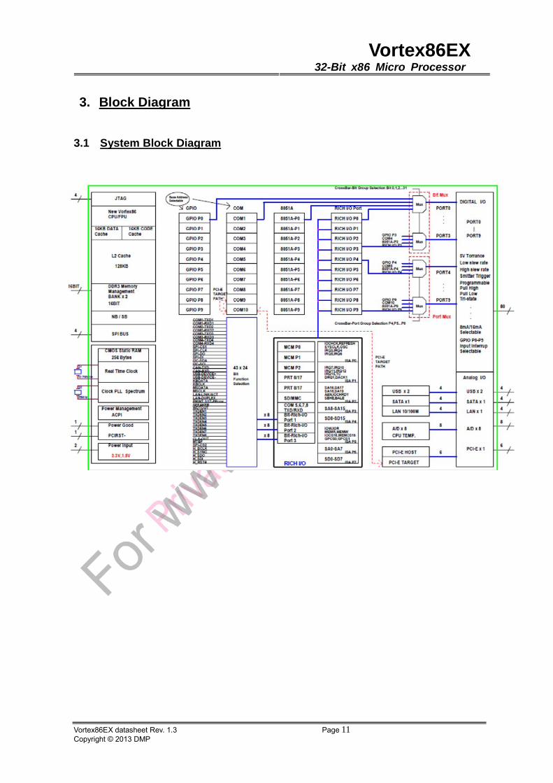
3. Block Diagram
3.1 System Block Diagram
Vortex86EX32-Bit x86 Micro Processor
Vortex86EX datasheet Rev. 1.3 Page 12Copyright © 2013 DMP
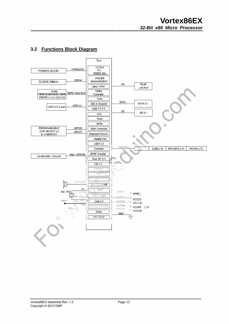
3.2 Functions Block Diagram
Vortex86EX32-Bit x86 Micro Processor
Vortex86EX datasheet Rev. 1.3 Page 13Copyright © 2013 DMP
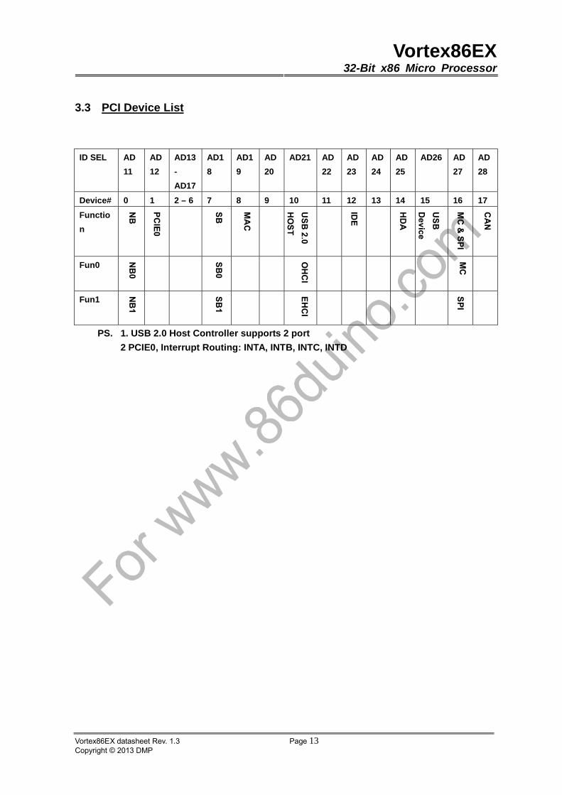
3.3 PCI Device List
ID SEL AD
11
AD
12
AD13
-
AD17
AD1
8
AD1
9
AD
20
AD21 AD
22
AD
23
AD
24
AD
25
AD26 AD
27
AD
28
Device# 0 1 2 – 6 7 8 9 10 11 12 13 14 15 16 17
Functio
n
Fun0
Fun1
PS. 1. USB 2.0 Host Controller supports 2 port
2 PCIE0, Interrupt Routing: INTA, INTB, INTC, INTD
Vortex86EX32-Bit x86 Micro Processor
Vortex86EX datasheet Rev. 1.3 Page 14Copyright © 2013 DMP
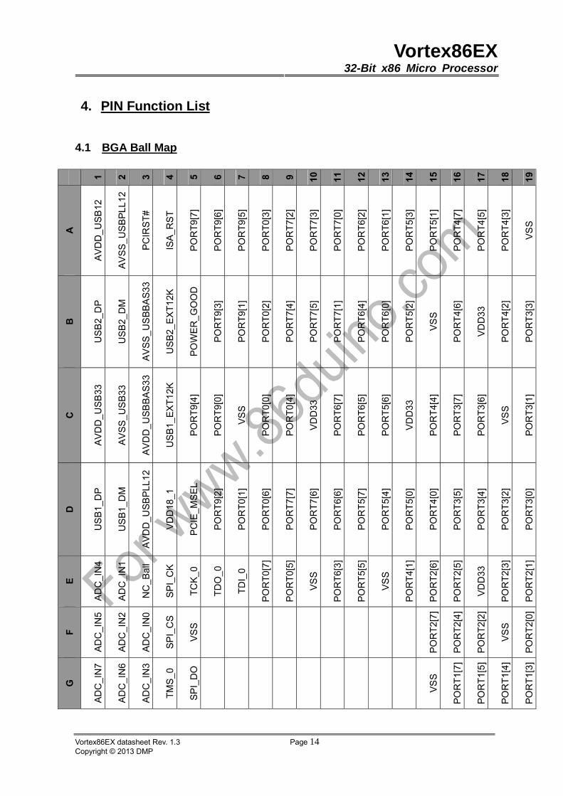
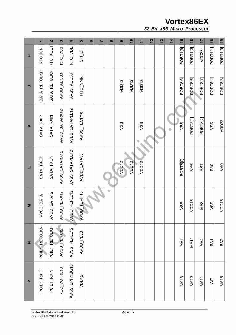
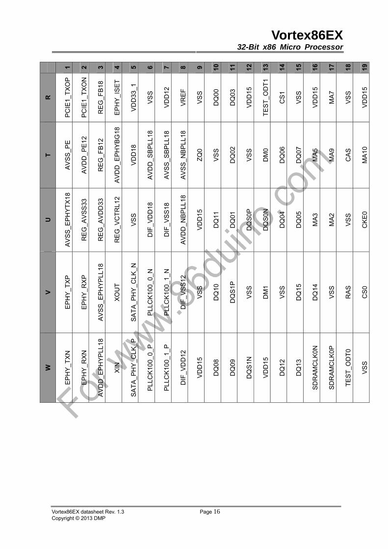
4. PIN Function List
4.1 BGA Ball Map
Vortex86EX32-Bit x86 Micro Processor
Vortex86EX datasheet Rev. 1.3 Page 15Copyright © 2013 DMP
Vortex86EX32-Bit x86 Micro Processor
Vortex86EX datasheet Rev. 1.3 Page 16Copyright © 2013 DMP
Vortex86EX32-Bit x86 Micro Processor
Vortex86EX datasheet Rev. 1.3 Page 17Copyright © 2013 DMP
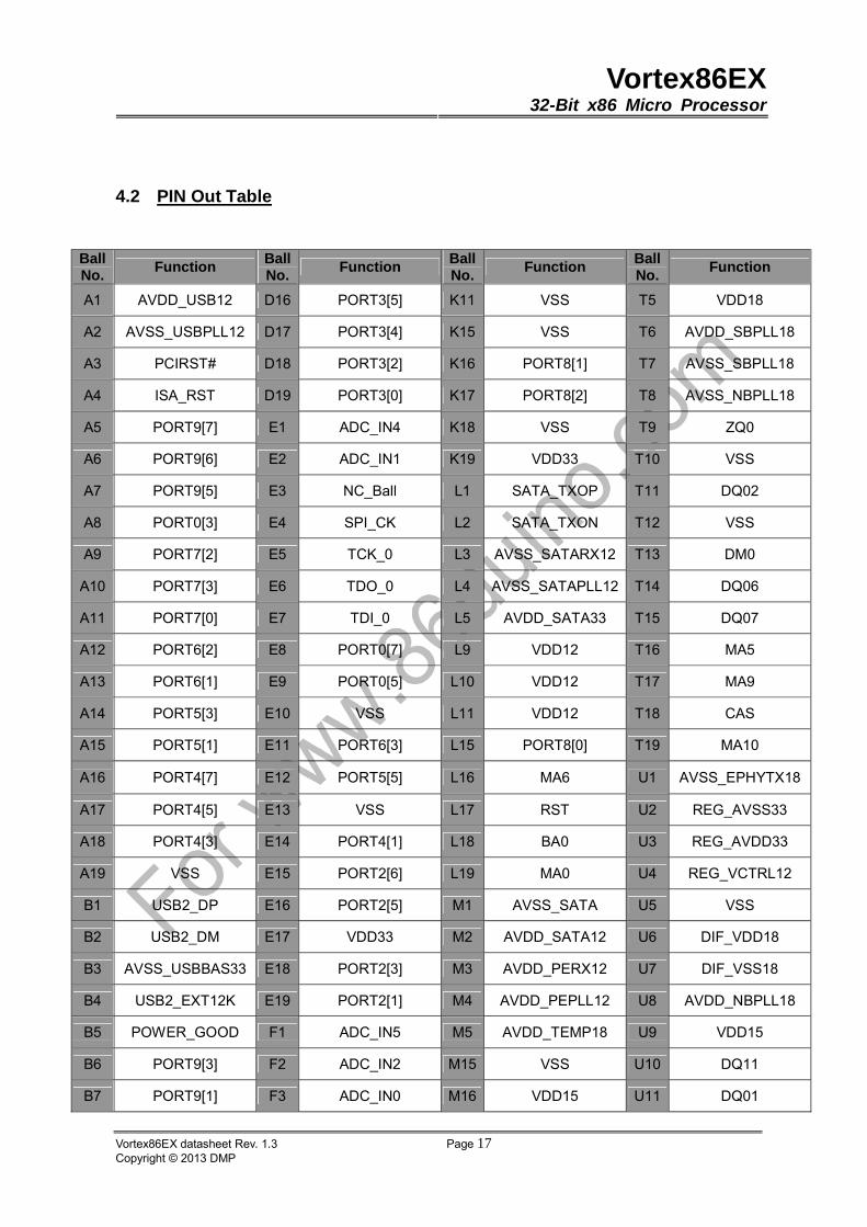
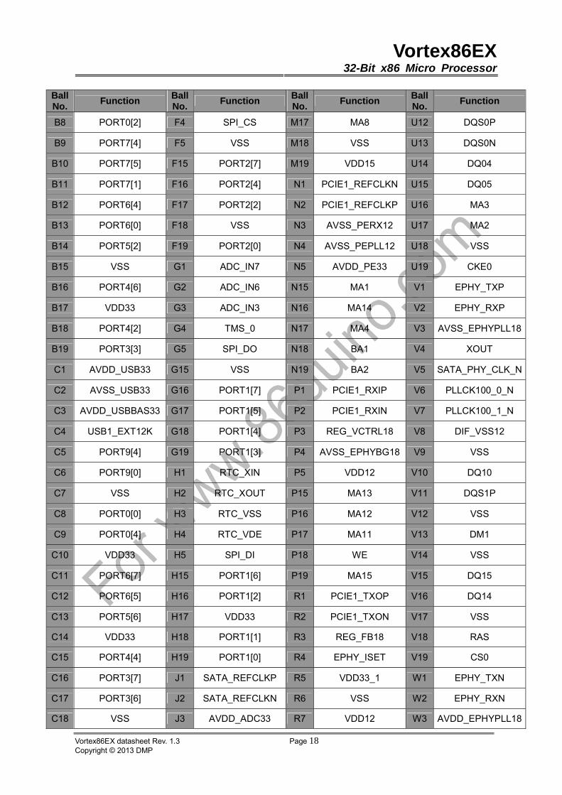
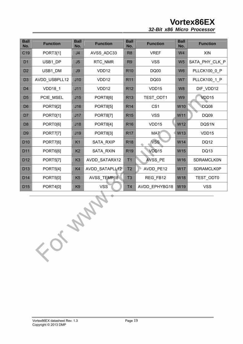
4.2 PIN Out Table
Ball No.
Function Ball No.
Function Ball No.
Function Ball No.
Function
A1 AVDD_USB12 D16 PORT3[5] K11 VSS T5 VDD18
A2 AVSS_USBPLL12 D17 PORT3[4] K15 VSS T6 AVDD_SBPLL18
A3 PCIRST# D18 PORT3[2] K16 PORT8[1] T7 AVSS_SBPLL18
A4 ISA_RST D19 PORT3[0] K17 PORT8[2] T8 AVSS_NBPLL18
A5 PORT9[7] E1 ADC_IN4 K18 VSS T9 ZQ0
A6 PORT9[6] E2 ADC_IN1 K19 VDD33 T10 VSS
A7 PORT9[5] E3 NC_Ball L1 SATA_TXOP T11 DQ02
A8 PORT0[3] E4 SPI_CK L2 SATA_TXON T12 VSS
A9 PORT7[2] E5 TCK_0 L3 AVSS_SATARX12 T13 DM0
A10 PORT7[3] E6 TDO_0 L4 AVSS_SATAPLL12 T14 DQ06
A11 PORT7[0] E7 TDI_0 L5 AVDD_SATA33 T15 DQ07
A12 PORT6[2] E8 PORT0[7] L9 VDD12 T16 MA5
A13 PORT6[1] E9 PORT0[5] L10 VDD12 T17 MA9
A14 PORT5[3] E10 VSS L11 VDD12 T18 CAS
A15 PORT5[1] E11 PORT6[3] L15 PORT8[0] T19 MA10
A16 PORT4[7] E12 PORT5[5] L16 MA6 U1 AVSS_EPHYTX18
A17 PORT4[5] E13 VSS L17 RST U2 REG_AVSS33
A18 PORT4[3] E14 PORT4[1] L18 BA0 U3 REG_AVDD33
A19 VSS E15 PORT2[6] L19 MA0 U4 REG_VCTRL12
B1 USB2_DP E16 PORT2[5] M1 AVSS_SATA U5 VSS
B2 USB2_DM E17 VDD33 M2 AVDD_SATA12 U6 DIF_VDD18
B3 AVSS_USBBAS33 E18 PORT2[3] M3 AVDD_PERX12 U7 DIF_VSS18
B4 USB2_EXT12K E19 PORT2[1] M4 AVDD_PEPLL12 U8 AVDD_NBPLL18
B5 POWER_GOOD F1 ADC_IN5 M5 AVDD_TEMP18 U9 VDD15
B6 PORT9[3] F2 ADC_IN2 M15 VSS U10 DQ11
B7 PORT9[1] F3 ADC_IN0 M16 VDD15 U11 DQ01
Vortex86EX32-Bit x86 Micro Processor
Vortex86EX datasheet Rev. 1.3 Page 18Copyright © 2013 DMP
Ball No.
Function Ball No.
Function Ball No.
Function Ball No.
Function
B8 PORT0[2] F4 SPI_CS M17 MA8 U12 DQS0P
B9 PORT7[4] F5 VSS M18 VSS U13 DQS0N
B10 PORT7[5] F15 PORT2[7] M19 VDD15 U14 DQ04
B11 PORT7[1] F16 PORT2[4] N1 PCIE1_REFCLKN U15 DQ05
B12 PORT6[4] F17 PORT2[2] N2 PCIE1_REFCLKP U16 MA3
B13 PORT6[0] F18 VSS N3 AVSS_PERX12 U17 MA2
B14 PORT5[2] F19 PORT2[0] N4 AVSS_PEPLL12 U18 VSS
B15 VSS G1 ADC_IN7 N5 AVDD_PE33 U19 CKE0
B16 PORT4[6] G2 ADC_IN6 N15 MA1 V1 EPHY_TXP
B17 VDD33 G3 ADC_IN3 N16 MA14 V2 EPHY_RXP
B18 PORT4[2] G4 TMS_0 N17 MA4 V3 AVSS_EPHYPLL18
B19 PORT3[3] G5 SPI_DO N18 BA1 V4 XOUT
C1 AVDD_USB33 G15 VSS N19 BA2 V5 SATA_PHY_CLK_N
C2 AVSS_USB33 G16 PORT1[7] P1 PCIE1_RXIP V6 PLLCK100_0_N
C3 AVDD_USBBAS33 G17 PORT1[5] P2 PCIE1_RXIN V7 PLLCK100_1_N
C4 USB1_EXT12K G18 PORT1[4] P3 REG_VCTRL18 V8 DIF_VSS12
C5 PORT9[4] G19 PORT1[3] P4 AVSS_EPHYBG18 V9 VSS
C6 PORT9[0] H1 RTC_XIN P5 VDD12 V10 DQ10
C7 VSS H2 RTC_XOUT P15 MA13 V11 DQS1P
C8 PORT0[0] H3 RTC_VSS P16 MA12 V12 VSS
C9 PORT0[4] H4 RTC_VDE P17 MA11 V13 DM1
C10 VDD33 H5 SPI_DI P18 WE V14 VSS
C11 PORT6[7] H15 PORT1[6] P19 MA15 V15 DQ15
C12 PORT6[5] H16 PORT1[2] R1 PCIE1_TXOP V16 DQ14
C13 PORT5[6] H17 VDD33 R2 PCIE1_TXON V17 VSS
C14 VDD33 H18 PORT1[1] R3 REG_FB18 V18 RAS
C15 PORT4[4] H19 PORT1[0] R4 EPHY_ISET V19 CS0
C16 PORT3[7] J1 SATA_REFCLKP R5 VDD33_1 W1 EPHY_TXN
C17 PORT3[6] J2 SATA_REFCLKN R6 VSS W2 EPHY_RXN
C18 VSS J3 AVDD_ADC33 R7 VDD12 W3 AVDD_EPHYPLL18
Vortex86EX32-Bit x86 Micro Processor
Vortex86EX datasheet Rev. 1.3 Page 19Copyright © 2013 DMP
Ball No.
Function Ball No.
Function Ball No.
Function Ball No.
Function
C19 PORT3[1] J4 AVSS_ADC33 R8 VREF W4 XIN
D1 USB1_DP J5 RTC_NMR R9 VSS W5 SATA_PHY_CLK_P
D2 USB1_DM J9 VDD12 R10 DQ00 W6 PLLCK100_0_P
D3 AVDD_USBPLL12 J10 VDD12 R11 DQ03 W7 PLLCK100_1_P
D4 VDD18_1 J11 VDD12 R12 VDD15 W8 DIF_VDD12
D5 PCIE_MSEL J15 PORT8[6] R13 TEST_ODT1 W9 VDD15
D6 PORT9[2] J16 PORT8[5] R14 CS1 W10 DQ08
D7 PORT0[1] J17 PORT8[7] R15 VSS W11 DQ09
D8 PORT0[6] J18 PORT8[4] R16 VDD15 W12 DQS1N
D9 PORT7[7] J19 PORT8[3] R17 MA7 W13 VDD15
D10 PORT7[6] K1 SATA_RXIP R18 VSS W14 DQ12
D11 PORT6[6] K2 SATA_RXIN R19 VDD15 W15 DQ13
D12 PORT5[7] K3 AVDD_SATARX12 T1 AVSS_PE W16 SDRAMCLK0N
D13 PORT5[4] K4 AVDD_SATAPLL12 T2 AVDD_PE12 W17 SDRAMCLK0P
D14 PORT5[0] K5 AVSS_TEMP18 T3 REG_FB12 W18 TEST_ODT0
D15 PORT4[0] K9 VSS T4 AVDD_EPHYBG18 W19 VSS

Vortex86EX32-Bit x86 Micro Processor
Vortex86EX datasheet Rev. 1.3 Page 20Copyright © 2013 DMP
4.3 Pin List Table
Function Symbol PIN
Sum
SYSTEM PWRGOOD, XOUT_25, XIN_25, PCIRST#, STRAP_PE_HTS 5 PINs
DDRIII Interface
DRAMRST#, DRAMCLK, DRAMCLK#, RAS#, CAS#, WE#, CKE,
CS1#, CS0#, DQM[1:0], DQS[1:0], DQS#[1:0], ODT[1], ODT[0],
BA[2:0],MD[15:0], MA[15:0], ZQ, VREF
54 PINs
CrossBar
Interface
CBAR_P0[7:0], CBAR_P1[7:0], CBAR_P2[7:0], CBAR_P3[7:0],
CBAR_P4[7:0], CBAR_P5[7:0], CBAR_P6[7:0], CBAR_P7[7:0],
CBAR_P8[7:0], CBAR_P9[7:0], CBAR_DEVRST
81 PINs
USB Interface USB_DP,USB_DM, USB1_DP, USB1_DM, USB_REXT,
USB_REXT1 6 PINs
PCIE
Bus Interface
PE0_CLKP, PE0_CLKN, PE0_TXP, PE0_TXN, PE0_RXP,
PE0_RXN, , DIF0_PCIE_PLLCLK100_P,
DIF0_PCIE_PLLCLK100_N, DIF1_CLK100_P, DIF1_CLK100_N
10 PINs
SATA InterfaceSATA_CLKP, SATA_CLKN, SATA_TXP, SATA_TXN, SATA_RXP,
SATA_RXN, DIF1_SATA_PHY_CLK_P, DIF1_SATA_PHY_CLK_N 8 PINs
Ethernet
Interface
ISET, TXN, TXP, RXN, RXP 5 PINs
SPI Interface SPI_CS#/ STRAP_BMS, SPI_CK/STRAP_JTAG,
SPI_DO/STRAP_HDM, SPI_DI 4 PINs
RTC Interface RTC_PS, RTC_XOUT, RTC_XIN 3 PINs
JTAG Interface TDO, TMS, TCK, TDI 4 PINs
ADC Interface ADC_IN0, ADC_IN1, ADC_IN2, ADC_IN3, ADC_IN4, ADC_IN5,
ADC_IN6, ADC_IN7, 8 PINs
Embedded
Regulator
REG_AVDD33, REG_AVSS33, REG_VCTRL18, REG_FB18,
REG_VCTRL12, REG_FB12 6 PINs
USB Power
Interface
AVDD_USB33, AVSS_USB33, AVDD_USB12, AVDD_USBBAS33,
AVSS_USBBAS33, AVDD_USBPLL12, AVSS_USBPLL12 7 PINs
PCIE Power
Interface
AVDD_PE33, AVDD_PE12, AVSS_PE, AVDD_PEPLL12,
AVSS_PEPLL12, AVDD_PERX12, AVSS_PERX12 5 PINs
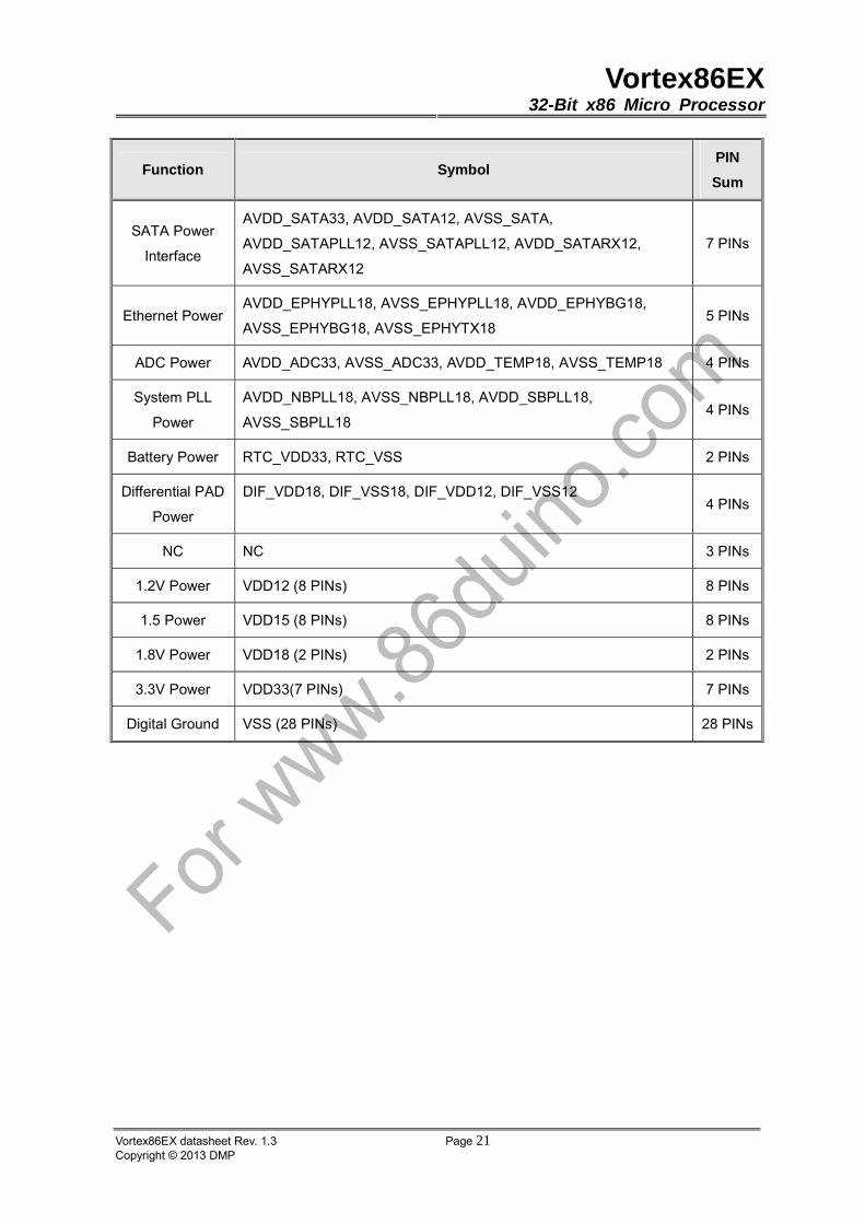
Vortex86EX32-Bit x86 Micro Processor
Vortex86EX datasheet Rev. 1.3 Page 21Copyright © 2013 DMP
Function Symbol PIN
Sum
SATA Power
Interface
AVDD_SATA33, AVDD_SATA12, AVSS_SATA,
AVDD_SATAPLL12, AVSS_SATAPLL12, AVDD_SATARX12,
AVSS_SATARX12
7 PINs
Ethernet PowerAVDD_EPHYPLL18, AVSS_EPHYPLL18, AVDD_EPHYBG18,
AVSS_EPHYBG18, AVSS_EPHYTX18 5 PINs
ADC Power AVDD_ADC33, AVSS_ADC33, AVDD_TEMP18, AVSS_TEMP18 4 PINs
System PLL
Power
AVDD_NBPLL18, AVSS_NBPLL18, AVDD_SBPLL18,
AVSS_SBPLL18 4 PINs
Battery Power RTC_VDD33, RTC_VSS 2 PINs
Differential PAD
Power
DIF_VDD18, DIF_VSS18, DIF_VDD12, DIF_VSS12 4 PINs
NC NC 3 PINs
1.2V Power VDD12 (8 PINs) 8 PINs
1.5 Power VDD15 (8 PINs) 8 PINs
1.8V Power VDD18 (2 PINs) 2 PINs
3.3V Power VDD33(7 PINs) 7 PINs
Digital Ground VSS (28 PINs) 28 PINs

Vortex86EX32-Bit x86 Micro Processor
Vortex86EX datasheet Rev. 1.3 Page 22Copyright © 2013 DMP
4.4 Signal Description
This chapter provides a detailed description of SoC signals. A signal with the symbol ”#” at the end
of itself indicates that this pin is low active. Otherwise, it is high active.
The following notations are used to describe the signal types:
I Input pin
O Output pin
OD Output pin with open-drain
I/O Bi-directional Input/Output pin
System ( 5 PINs)
PIN No. Symbol Type Description
B5 PWRGOOD I
Power-Good Input. This signal comes from Power Good of
the power supply to indicate that the power is available. The
SoC uses this signal to generate reset sequence for the
system.
V4 XOUT_25 O Crystal-out. Frequency output from the inverting amplifier
(oscillator).
W4 XIN_25 I Crystal-in. 25MHz frequency input, within +/- 30 ppm
tolerance, to the amplifier (oscillator).
A3 PCIRST# O PCI Reset. This pin is used to reset PCI devices. When it is
asserted low, all the PCI devices will be reset.
D5 STRAP_PE_HT
S I
PCIe Host / Target Select. Strap pin for PCIe Interface is
selected to Host or Target mode.
Pull low to PCIe Target.
Pull high to PCIe Host. (default internal pull-high)
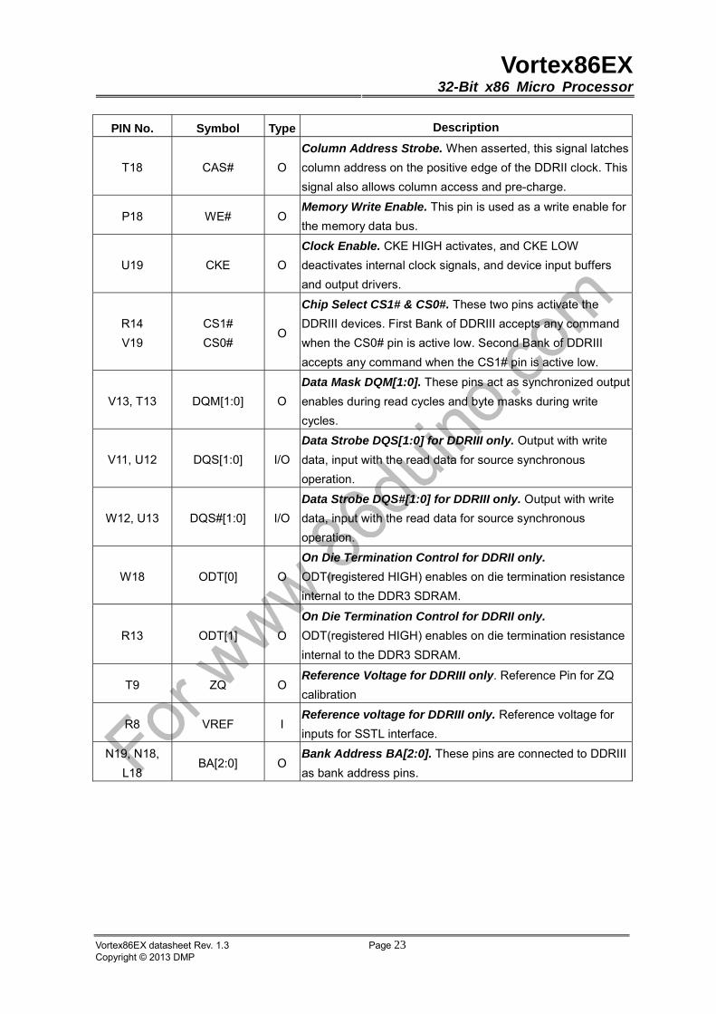
DDRIII Interface ( 54 PINs)
PIN No. Symbol Type Description
L17 DRAMRST# O
Active Low Asynchronous Reset. Reset is active when
RESET# is LOW and otherwise. RESET# must be set as
HIGH during normal operation.
W17
W16
DRAMCLK
DRAMCLK1 O
Clock output. This pin provides the fundamental timing for
the DDRII controller.
V18 RAS# O
Row Address Strobe. When asserted, this signal latches
row address on positive edge of the DDRII clock. This signal
also allows row access and pre-charge.
Vortex86EX32-Bit x86 Micro Processor
Vortex86EX datasheet Rev. 1.3 Page 23Copyright © 2013 DMP
PIN No. Symbol Type Description
T18 CAS# O
Column Address Strobe. When asserted, this signal latches
column address on the positive edge of the DDRII clock. This
signal also allows column access and pre-charge.
P18 WE# O Memory Write Enable. This pin is used as a write enable for
the memory data bus.
U19 CKE O
Clock Enable. CKE HIGH activates, and CKE LOW
deactivates internal clock signals, and device input buffers
and output drivers.
R14
V19
CS1#
CS0#O
Chip Select CS1# & CS0#. These two pins activate the
DDRIII devices. First Bank of DDRIII accepts any command
when the CS0# pin is active low. Second Bank of DDRIII
accepts any command when the CS1# pin is active low.
V13, T13 DQM[1:0] O
Data Mask DQM[1:0]. These pins act as synchronized output
enables during read cycles and byte masks during write
cycles.
V11, U12 DQS[1:0] I/O
Data Strobe DQS[1:0] for DDRIII only. Output with write
data, input with the read data for source synchronous
operation.
W12, U13 DQS#[1:0] I/O
Data Strobe DQS#[1:0] for DDRIII only. Output with write
data, input with the read data for source synchronous
operation.
W18 ODT[0] O
On Die Termination Control for DDRII only.
ODT(registered HIGH) enables on die termination resistance
internal to the DDR3 SDRAM.
R13 ODT[1] O
On Die Termination Control for DDRII only.
ODT(registered HIGH) enables on die termination resistance
internal to the DDR3 SDRAM.
T9 ZQ O Reference Voltage for DDRIII only. Reference Pin for ZQ
calibration
R8 VREF I Reference voltage for DDRIII only. Reference voltage for
inputs for SSTL interface.
N19, N18,
L18 BA[2:0] O
Bank Address BA[2:0]. These pins are connected to DDRIII
as bank address pins.
Vortex86EX32-Bit x86 Micro Processor
Vortex86EX datasheet Rev. 1.3 Page 24Copyright © 2013 DMP
PIN No. Symbol Type Description
V15, V16,
W15, W14,
U10, V10,
W11, W10,
T15, T14,
U15, U14,
R11, T11,
U11, R10
MD[15:0] I/OMemory Data MD[15:0]. These pins are connected to the
DDRIII data bus.
P19, N16,
P15, P16,
P17, T19,
T17, M17,
R17, L16,
T16, N17,
U16, U17,
N15, L19
MA[15:0] O Memory Address MA[15-0]. Normally, these pins are used
as the row and column address for DDRIII.
Vortex86EX32-Bit x86 Micro Processor
Vortex86EX datasheet Rev. 1.3 Page 25Copyright © 2013 DMP
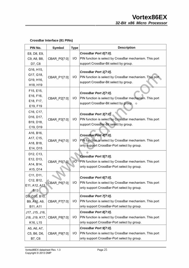
CrossBar Interface (81 PINs)
PIN No. Symbol Type Description
E8, D8, E9,
C9, A8, B8,
D7, C8
CBAR_P0[7:0] I/O
CrossBar Port 0[7:0].
PIN function is select by CrossBar mechanism. This port
support CrossBar-Bit select by group.
G16, H15,
G17, G18,
G19, H16,
H18, H19
CBAR_P1[7:0] I/O
CrossBar Port 1[7:0].
PIN function is select by CrossBar mechanism. This port
support CrossBar-Bit select by group.
F15, E15,
E16, F16,
E18, F17,
E19, F19
CBAR_P2[7:0] I/O
CrossBar Port 2[7:0].
PIN function is select by CrossBar mechanism. This port
support CrossBar-Bit select by group.
C16, C17,
D16, D17,
B19, D18,
C19, D19
CBAR_P3[7:0] I/O
CrossBar Port 3[7:0].
PIN function is select by CrossBar mechanism. This port
support CrossBar-Bit select by group.
A16, B16,
A17, C15,
A18, B18,
E14, D15
CBAR_P4[7:0] I/O
CrossBar Port 4[7:0].
PIN function is select by CrossBar mechanism. This port
only support CrossBar-Port select by group.
D12, C13,
E12, D13,
A14, B14,
A15, D14
CBAR_P5[7:0] I/O
CrossBar Port 5[7:0].
PIN function is select by CrossBar mechanism. This port
only support CrossBar-Port select by group.
C11, D11,
C12, B12,
E11, A12, A13,
B13
CBAR_P6[7:0] I/O
CrossBar Port 6[7:0].
PIN function is select by CrossBar mechanism. This port
only support CrossBar-Port select by group.
D9, D10, B10,
B9, A10, A9,
B11, A11
CBAR_P7[7:0] I/O
CrossBar Port 7[7:0].
PIN function is select by CrossBar mechanism. This port
only support CrossBar-Port select by group.
J17, J15, J16,
J18, J19, K17,
K16, L15
CBAR_P8[7:0] I/O
CrossBar Port 8[7:0].
PIN function is select by CrossBar mechanism. This port
only support CrossBar-Port select by group.
A5, A6, A7,
C5, B6, D6,
B7, C6
CBAR_P9[7:0] I/O
CrossBar Port 9[7:0].
PIN function is select by CrossBar mechanism. This port
only support CrossBar-Port select by group.

Vortex86EX32-Bit x86 Micro Processor
Vortex86EX datasheet Rev. 1.3 Page 26Copyright © 2013 DMP
PIN No. Symbol Type Description
A4 CBAR_DEVRS
T O
CrossBar Device Reset
This reset signal is manual controled by software for device
accessed in CrossBar.
USB Interface (6 PINs)
PIN No. Symbol Type Description
D1
D2
USB_DP
USB_DM I/O
Universal Serial Bus Controller 0 Port 0. These are the serial
data pair for USB Port 0. 15kΩ pull down resistors are
connected to DP and DM internally.
B1
B2
USB1_DP
USB1_DM I/O
Universal Serial Bus Controller 0 Port 1. These are the serial
data pair for USB Port 1. 15kΩ pull down resistors are
connected to DP and DM internally.
C4 USB_REXT I Universal Serial Bus Controller 0 External Reference
Resistance 12kΩ ±1%
B4 USB_REXT1 I Universal Serial Bus Controller 1 External Reference
Resistance 12kΩ ±1%
PCIE Bus Interface ( 10 PINs)
PIN No. Symbol Type Description
P1
P2
PE0_RXP
PE0_RXN I PCI-E Differential serial data input. P: positive; N:negative
R1
R2
PE0_TXP
PE0_TXN O PCI-E Differential serial data output. P: positive; N: negative
N2
N1
PE0_CLKP
PE0_CLKN I PCI-E Differential reference clock. P: positive; N: negative
W6
V6
DIF0_PCIE_PLL
CLK100_P
DIF0_PCIE_PLL
CLK100_N
O PCI-E Differential Clock 100MHz from Internal PLL
P: positive; N: negative
W7
V7
DIF1_CLK100_
P
DIF1_CLK100_
N
O PCI-E Differential Clock 100MHz to Port0
P: positive; N: negative
Vortex86EX32-Bit x86 Micro Processor
Vortex86EX datasheet Rev. 1.3 Page 27Copyright © 2013 DMP
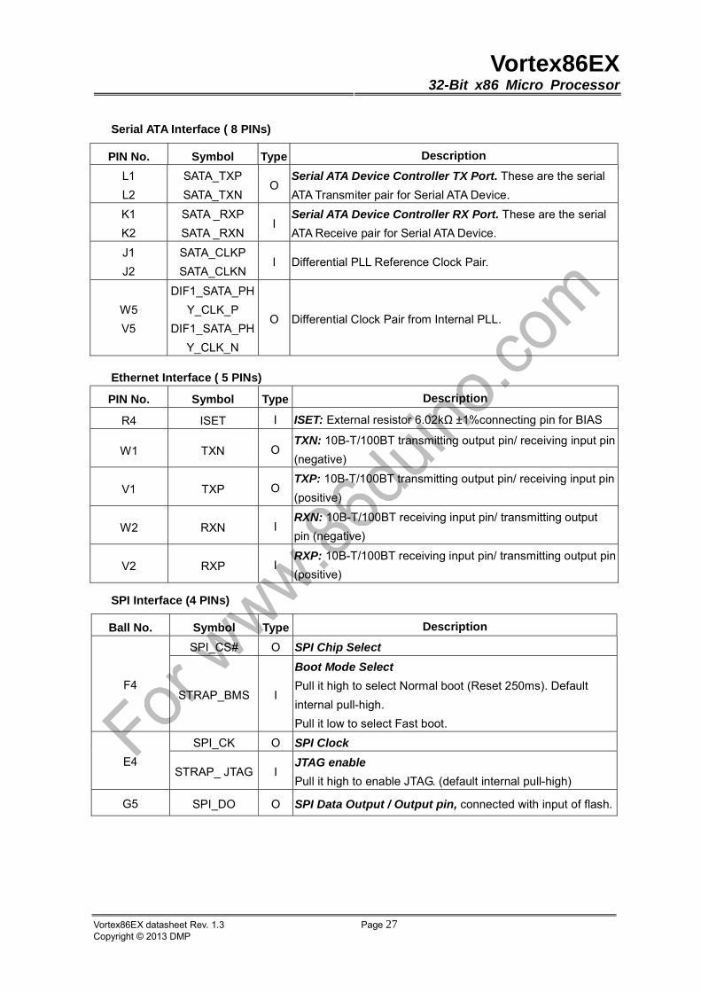
Serial ATA Interface ( 8 PINs)
PIN No. Symbol Type Description
L1
L2
SATA_TXP
SATA_TXN O
Serial ATA Device Controller TX Port. These are the serial
ATA Transmiter pair for Serial ATA Device.
K1
K2
SATA _RXP
SATA _RXN I
Serial ATA Device Controller RX Port. These are the serial
ATA Receive pair for Serial ATA Device.
J1
J2
SATA_CLKP
SATA_CLKN I Differential PLL Reference Clock Pair.
W5
V5
DIF1_SATA_PH
Y_CLK_P
DIF1_SATA_PH
Y_CLK_N
O Differential Clock Pair from Internal PLL.
Ethernet Interface ( 5 PINs)
PIN No. Symbol Type Description
R4 ISET I ISET: External resistor 6.02kΩ ±1%connecting pin for BIAS
W1 TXN O TXN: 10B-T/100BT transmitting output pin/ receiving input pin
(negative)
V1 TXP O TXP: 10B-T/100BT transmitting output pin/ receiving input pin
(positive)
W2 RXN I RXN: 10B-T/100BT receiving input pin/ transmitting output
pin (negative)
V2 RXP I RXP: 10B-T/100BT receiving input pin/ transmitting output pin
(positive)
SPI Interface (4 PINs)
Ball No. Symbol Type Description
SPI_CS# O SPI Chip Select
F4 STRAP_BMS I
Boot Mode Select
Pull it high to select Normal boot (Reset 250ms). Default
internal pull-high.
Pull it low to select Fast boot.
SPI_CK O SPI Clock
E4 STRAP_ JTAG I
JTAG enable
Pull it high to enable JTAG. (default internal pull-high)
G5 SPI_DO O SPI Data Output / Output pin, connected with input of flash.
Vortex86EX32-Bit x86 Micro Processor
Vortex86EX datasheet Rev. 1.3 Page 28Copyright © 2013 DMP
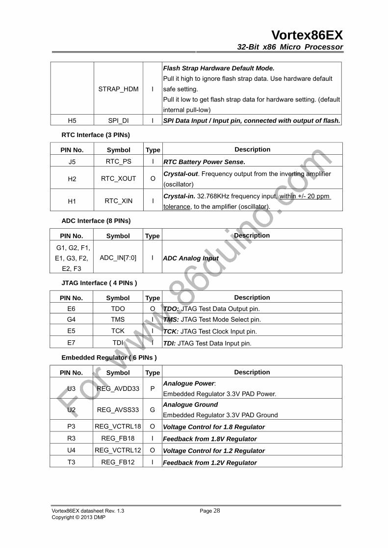
STRAP_HDM I
Flash Strap Hardware Default Mode.
Pull it high to ignore flash strap data. Use hardware default
safe setting.
Pull it low to get flash strap data for hardware setting. (default
internal pull-low)
H5 SPI_DI I SPI Data Input / Input pin, connected with output of flash.
RTC Interface (3 PINs)
PIN No. Symbol Type Description
J5 RTC_PS I RTC Battery Power Sense.
H2 RTC_XOUT O Crystal-out. Frequency output from the inverting amplifier
(oscillator)
H1 RTC_XIN I Crystal-in. 32.768KHz frequency input, within +/- 20 ppm
tolerance, to the amplifier (oscillator).
ADC Interface (8 PINs)
PIN No. Symbol Type Description
G1, G2, F1,
E1, G3, F2,
E2, F3
ADC_IN[7:0] I ADC Analog Input
JTAG Interface ( 4 PINs )
PIN No. Symbol Type Description
E6 TDO O TDO: JTAG Test Data Output pin.
G4 TMS I TMS: JTAG Test Mode Select pin.
E5 TCK I TCK: JTAG Test Clock Input pin.
E7 TDI I TDI: JTAG Test Data Input pin.
Embedded Regulator ( 6 PINs )
PIN No. Symbol Type Description
U3 REG_AVDD33 P Analogue Power:
Embedded Regulator 3.3V PAD Power.
U2 REG_AVSS33 G Analogue Ground
Embedded Regulator 3.3V PAD Ground
P3 REG_VCTRL18 O Voltage Control for 1.8 Regulator
R3 REG_FB18 I Feedback from 1.8V Regulator
U4 REG_VCTRL12 O Voltage Control for 1.2 Regulator
T3 REG_FB12 I Feedback from 1.2V Regulator
Vortex86EX32-Bit x86 Micro Processor
Vortex86EX datasheet Rev. 1.3 Page 29Copyright © 2013 DMP
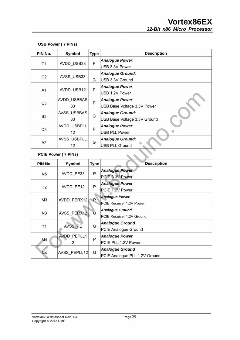
USB Power ( 7 PINs)
PIN No. Symbol Type Description
C1 AVDD_USB33 P Analogue Power:
USB 3.3V Power
C2 AVSS_USB33G
Analogue Ground:
USB 3.3V Ground
A1 AVDD_USB12 P Analogue Power:
USB 1.2V Power
C3 AVDD_USBBAS
33 P
Analogue Power:
USB Base Voltage 3.3V Power
B3 AVSS_USBBAS
33 G
Analogue Ground:
USB Base Voltage 3.3V Ground
D3 AVDD_USBPLL
12 P
Analogue Power:
USB PLL Power
A2 AVSS_USBPLL
12 G
Analogue Ground:
USB PLL Ground
PCIE Power ( 7 PINs)
PIN No. Symbol Type Description
N5 AVDD_PE33 P Analogue Power
PCIE 3.3V Power
T2 AVDD_PE12 P Analogue Power
PCIE 1.2V Power
M3 AVDD_PERX12 PAnalogue Power
PCIE Receiver 1.2V Power
N3 AVSS_PERX12 G Analogue Ground
PCIE Receiver 1.2V Ground
T1 AVSS_PE G Analogue Ground
PCIE Analogue Ground
M4 AVDD_PEPLL1
2 P
Analogue Power
PCIE PLL 1.2V Power
N4 AVSS_PEPLL12 G Analogue Ground
PCIE Analogue PLL 1.2V Ground

Vortex86EX32-Bit x86 Micro Processor
Vortex86EX datasheet Rev. 1.3 Page 30Copyright © 2013 DMP
SATA Power ( 7 PINs)
PIN No. Symbol Type Description
L5 AVDD_SATA33 P Analogue Power
SATA PHY: 3.3V Analogue Power
M2 AVDD_SATA12 P Analogue Power
SATA PHY: 1.2V Analogue Power
M1 AVSS_SATA G Analogue Ground
SATA PHY: Analogue Ground
K3 AVDD_SATARX
12 P
Analogue Power
SATA PHY: Receiver 1.2V Analogue Power
L3 AVSS_SATARX
12 G
Analogue Ground
SATA PHY: Receiver Analogue Ground
K4 AVDD_SATAPL
L12 P
Analogue Power
SATA PHY: PLL 1.2V Analogue Power
L4 AVSS_SATAPLL
12 G
Analogue Ground
SATA PHY: PLL Analogue Ground
Ethernet Power ( 5 PINs)
PIN No. Symbol Type Description
W3 AVDD_EPHYPL
L18 P
Analogue Power
Internal Ethernet PHY PLL 1.8V Power
V3 AVSS_EPHYPL
L18 G
Analogue Ground
Internal Ethernet PHY PLL 1.8V Ground
T4 AVDD_EPHYB
G18 P
Analogue Power
Internal Ethernet PHY Band Gap 1.8V Power
P4 AVSS_EPHYBG
18 G
Analogue Ground
Internal Ethernet PHY Band Gap 1.8V Ground
U1 AVSS_EPHYTX
18 G
Analogue Ground
Internal Ethernet PHY TX 1.8V Ground
Vortex86EX32-Bit x86 Micro Processor
Vortex86EX datasheet Rev. 1.3 Page 31Copyright © 2013 DMP
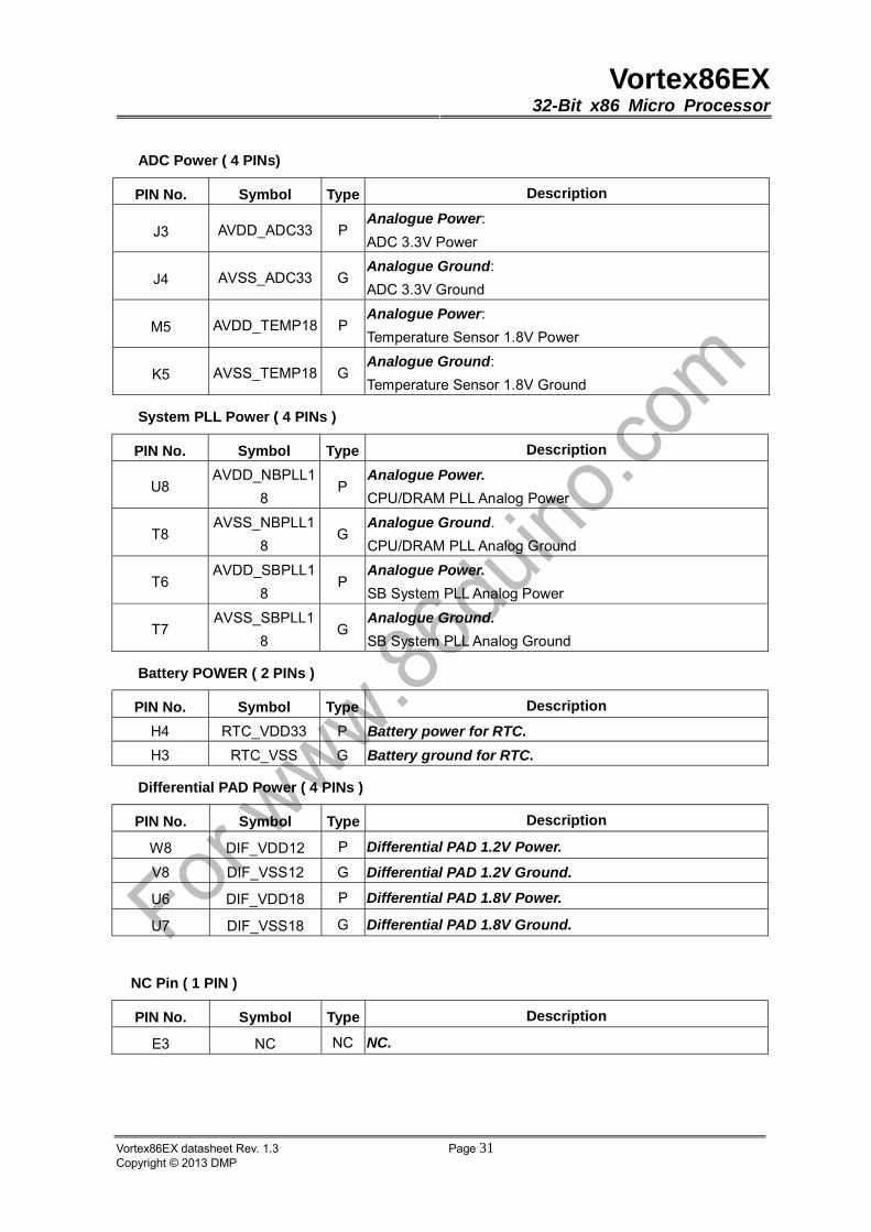
ADC Power ( 4 PINs)
PIN No. Symbol Type Description
J3 AVDD_ADC33 P Analogue Power:
ADC 3.3V Power
J4 AVSS_ADC33 G Analogue Ground:
ADC 3.3V Ground
M5 AVDD_TEMP18 P Analogue Power:
Temperature Sensor 1.8V Power
K5 AVSS_TEMP18 G Analogue Ground:
Temperature Sensor 1.8V Ground
System PLL Power ( 4 PINs )
PIN No. Symbol Type Description
U8 AVDD_NBPLL1
8 P
Analogue Power.
CPU/DRAM PLL Analog Power
T8 AVSS_NBPLL1
8 G
Analogue Ground.
CPU/DRAM PLL Analog Ground
T6 AVDD_SBPLL1
8 P
Analogue Power.
SB System PLL Analog Power
T7 AVSS_SBPLL1
8 G
Analogue Ground.
SB System PLL Analog Ground
Battery POWER ( 2 PINs )
PIN No. Symbol Type Description
H4 RTC_VDD33 P Battery power for RTC.
H3 RTC_VSS G Battery ground for RTC.
Differential PAD Power ( 4 PINs )
PIN No. Symbol Type Description
W8 DIF_VDD12 P Differential PAD 1.2V Power.
V8 DIF_VSS12 G Differential PAD 1.2V Ground.
U6 DIF_VDD18 P Differential PAD 1.8V Power.
U7 DIF_VSS18 G Differential PAD 1.8V Ground.
NC Pin ( 1 PIN )
PIN No. Symbol Type Description
E3 NC NC NC.

Vortex86EX32-Bit x86 Micro Processor
Vortex86EX datasheet Rev. 1.3 Page 32Copyright © 2013 DMP
1.2V POWER ( 8 PINs)
PIN No. Symbol Type Description
J10, J11, J9,
L10, L11, L9,
P5, R7
VDD12 P Core power.
1.5V POWER ( 8 PINs)
PIN No. Symbol Type Description
M16, M19,
R12, R16,
R19, U9,
W13, W9
VDD15 P 1.5V DDR Power.
1.8V POWER ( 2 PINs)
PIN No. Symbol Type Description
T5, D4 VDD18 P 1.8V Power.
3.3V Power ( 7 PINs )
PIN No. Symbol Type Description
B17, C10,
C14, E17,
H17, K19, R5
VDD33 P I/O PAD Power.
Digital Ground ( 28 PINs )
PIN No. Symbol Type Description
A19, B15,
C18, C7, E10,
E13, F18, F5,
G15, K11,
K15, K18, K9,
M15, M18,
R15, R18,
R6, R9, T10,
T12, U18, U5,
V12, V14,
V17, V9, W19
VSS G Digital Ground.
Vortex86EX32-Bit x86 Micro Processor
Vortex86EX datasheet Rev. 1.3 Page 33Copyright © 2013 DMP
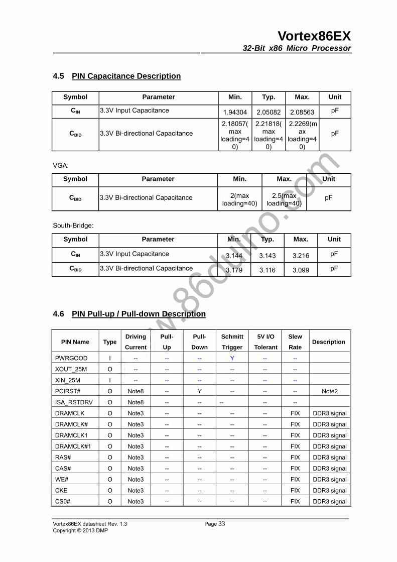
4.5 PIN Capacitance Description
Symbol Parameter Min. Typ. Max. Unit
CIN 3.3V Input Capacitance 1.94304 2.05082 2.08563 pF
CBID 3.3V Bi-directional Capacitance
2.18057(max
loading=40)
2.21818(max
loading=40)
2.2269(max
loading=40)
pF
VGA:
Symbol Parameter Min. Max. Unit
CBID 3.3V Bi-directional Capacitance 2(max loading=40)
2.5(max loading=40)
pF
South-Bridge:
Symbol Parameter Min. Typ. Max. Unit
CIN 3.3V Input Capacitance 3.144 3.143 3.216 pF
CBID 3.3V Bi-directional Capacitance 3.179 3.116 3.099 pF
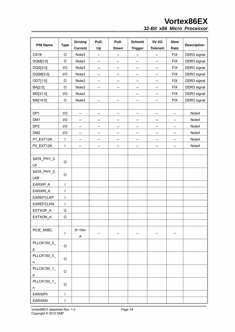
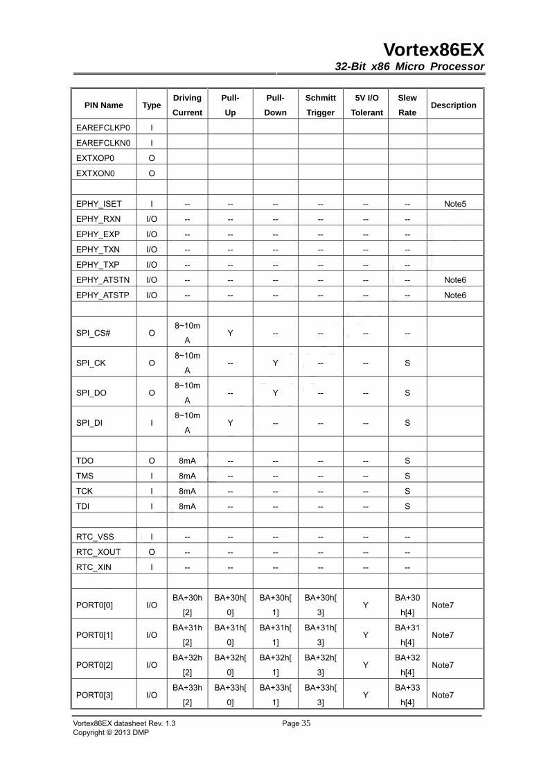
4.6 PIN Pull-up / Pull-down Description
PIN Name TypeDriving
Current
Pull-
Up
Pull-
Down
Schmitt
Trigger
5V I/O
Tolerant
Slew
Rate Description
PWRGOOD I -- -- -- Y -- --
XOUT_25M O -- -- -- -- -- --
XIN_25M I -- -- -- -- -- --
PCIRST# O Note8 -- Y -- -- -- Note2
ISA_RSTDRV O Note8 -- -- -- -- --
DRAMCLK O Note3 -- -- -- -- FIX DDR3 signal
DRAMCLK# O Note3 -- -- -- -- FIX DDR3 signal
DRAMCLK1 O Note3 -- -- -- -- FIX DDR3 signal
DRAMCLK#1 O Note3 -- -- -- -- FIX DDR3 signal
RAS# O Note3 -- -- -- -- FIX DDR3 signal
CAS# O Note3 -- -- -- -- FIX DDR3 signal
WE# O Note3 -- -- -- -- FIX DDR3 signal
CKE O Note3 -- -- -- -- FIX DDR3 signal
CS0# O Note3 -- -- -- -- FIX DDR3 signal
Vortex86EX32-Bit x86 Micro Processor
Vortex86EX datasheet Rev. 1.3 Page 34Copyright © 2013 DMP
PIN Name TypeDriving
Current
Pull-
Up
Pull-
Down
Schmitt
Trigger
5V I/O
Tolerant
Slew
Rate Description
CS1# O Note3 -- -- -- -- FIX DDR3 signal
DQM[3:0] O Note3 -- -- -- -- FIX DDR3 signal
DQS[3:0] I/O Note3 -- -- -- -- FIX DDR3 signal
DQS#[3:0] I/O Note3 -- -- -- -- FIX DDR3 signal
ODT[1:0] O Note3 -- -- -- -- FIX DDR3 signal
BA[2:0] O Note3 -- -- -- -- FIX DDR3 signal
MD[31:0] I/O Note3 -- -- FIX DDR3 signal
MA[14:0] O Note3 -- -- -- -- FIX DDR3 signal
DP1 I/O -- -- -- -- -- -- Note4
DM1 I/O -- -- -- -- -- -- Note4
DP2 I/O -- -- -- -- -- -- Note4
DM2 I/O -- -- -- -- -- -- Note4
P1_EXT12K I -- -- -- -- -- -- Note4
P2_EXT12K I -- -- -- -- -- -- Note4
SATA_PHY_C
LK O
SATA_PHY_C
LK# O
EARXIP_A I
EARXIN_A I
EAREFCLKP I
EAREFCLKN I
EXTXOP_A O
EXTXON_A O
PCIE_MSEL I
8~10m
A-- -- -- -- --
PLLCK100_0_
p O
PLLCK100_0_
n O
PLLCK100_1_
p O
PLLCK100_1_
n O
EARXIP0 I
EARXIN0 I
Vortex86EX32-Bit x86 Micro Processor
Vortex86EX datasheet Rev. 1.3 Page 35Copyright © 2013 DMP
PIN Name TypeDriving
Current
Pull-
Up
Pull-
Down
Schmitt
Trigger
5V I/O
Tolerant
Slew
Rate Description
EAREFCLKP0 I
EAREFCLKN0 I
EXTXOP0 O
EXTXON0 O
EPHY_ISET I -- -- -- -- -- -- Note5
EPHY_RXN I/O -- -- -- -- -- --
EPHY_EXP I/O -- -- -- -- -- --
EPHY_TXN I/O -- -- -- -- -- --
EPHY_TXP I/O -- -- -- -- -- --
EPHY_ATSTN I/O -- -- -- -- -- -- Note6
EPHY_ATSTP I/O -- -- -- -- -- -- Note6
SPI_CS# O 8~10m
A Y -- -- -- --
SPI_CK O 8~10m
A -- Y -- -- S
SPI_DO O 8~10m
A -- Y -- -- S
SPI_DI I 8~10m
A Y -- -- -- S
TDO O 8mA -- -- -- -- S
TMS I 8mA -- -- -- -- S
TCK I 8mA -- -- -- -- S
TDI I 8mA -- -- -- -- S
RTC_VSS I -- -- -- -- -- --
RTC_XOUT O -- -- -- -- -- --
RTC_XIN I -- -- -- -- -- --
PORT0[0] I/O BA+30h
[2]
BA+30h[
0]
BA+30h[
1]
BA+30h[
3] Y
BA+30
h[4] Note7
PORT0[1] I/O BA+31h
[2]
BA+31h[
0]
BA+31h[
1]
BA+31h[
3] Y
BA+31
h[4] Note7
PORT0[2] I/O BA+32h
[2]
BA+32h[
0]
BA+32h[
1]
BA+32h[
3] Y
BA+32
h[4] Note7
PORT0[3] I/O BA+33h
[2]
BA+33h[
0]
BA+33h[
1]
BA+33h[
3] Y
BA+33
h[4] Note7

Vortex86EX32-Bit x86 Micro Processor
Vortex86EX datasheet Rev. 1.3 Page 36Copyright © 2013 DMP
PIN Name TypeDriving
Current
Pull-
Up
Pull-
Down
Schmitt
Trigger
5V I/O
Tolerant
Slew
Rate Description
PORT0[4] I/O BA+34h
[2]
BA+34h[
0]
BA+34h[
1]
BA+34h[
3] Y
BA+34
h[4] Note7
PORT0[5] I/O BA+35h
[2]
BA+35h[
0]
BA+35h[
1]
BA+35h[
3] Y
BA+35
h[4] Note7
PORT0[6] I/O BA+36h
[2]
BA+36h[
0]
BA+36h[
1]
BA+36h[
3] Y
BA+36
h[4] Note7
PORT0[7] I/O BA+37h
[2]
BA+37h[
0]
BA+37h[
1]
BA+37h[
3] Y
BA+37
h[4] Note7
PORT1[0] I/O BA+38h
[2]
BA+38h[
0]
BA+38h[
1]
BA+38h[
3] Y
BA+38
h[4] Note7
PORT1[1] I/O BA+39h
[2]
BA+39h[
0]
BA+39h[
1]
BA+39h[
3] Y
BA+39
h[4] Note7
PORT1[2] I/O BA+3Ah
[2]
BA+3Ah[
0]
BA+3Ah[
1]
BA+3Ah[
3] Y
BA+3A
h[4] Note7
PORT1[3] I/O BA+3Bh
[2]
BA+3Bh[
0]
BA+3Bh[
1]
BA+3Bh[
3] Y
BA+3B
h[4] Note7
PORT1[4] I/O BA+3C
h[2]
BA+3Ch[
0]
BA+3Ch[
1]
BA+3Ch[
3] Y
BA+3C
h[4] Note7
PORT1[5] I/O BA+3D
h[2]
BA+3Dh[
0]
BA+3Dh[
1]
BA+3Dh[
3] Y
BA+3D
h[4] Note7
PORT1[6] I/O BA+3Eh
[2]
BA+3Eh[
0]
BA+3Eh[
1]
BA+3Eh[
3] Y
BA+3E
h[4] Note7
PORT1[7] I/O BA+3Fh
[2]
BA+3Fh[
0]
BA+3Fh[
1]
BA+3Fh[
3] Y
BA+3F
h[4] Note7
PORT2[0] I/O BA+40h
[2]
BA+40h[
0]
BA+40h[
1]
BA+40h[
3] Y
BA+40
h[4] Note7
PORT2[1] I/O BA+41h
[2]
BA+41h[
0]
BA+41h[
1]
BA+41h[
3] Y
BA+41
h[4] Note7
PORT2[2] I/O BA+42h
[2]
BA+42h[
0]
BA+42h[
1]
BA+42h[
3] Y
BA+42
h[4] Note7
PORT2[3] I/O BA+43h
[2]
BA+43h[
0]
BA+43h[
1]
BA+43h[
3] Y
BA+43
h[4] Note7
PORT2[4] I/O BA+44h
[2]
BA+44h[
0]
BA+44h[
1]
BA+44h[
3] Y
BA+44
h[4] Note7
PORT2[5] I/O BA+45h
[2]
BA+45h[
0]
BA+45h[
1]
BA+45h[
3] Y
BA+45
h[4] Note7
PORT2[6] I/O BA+46h BA+46h[ BA+46h[ BA+46h[ Y BA+46 Note7
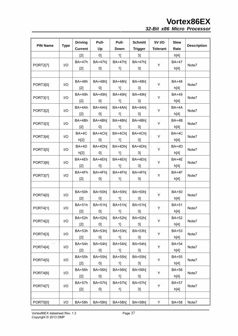
Vortex86EX32-Bit x86 Micro Processor
Vortex86EX datasheet Rev. 1.3 Page 37Copyright © 2013 DMP
PIN Name TypeDriving
Current
Pull-
Up
Pull-
Down
Schmitt
Trigger
5V I/O
Tolerant
Slew
Rate Description
[2] 0] 1] 3] h[4]
PORT2[7] I/O BA+47h
[2]
BA+47h[
0]
BA+47h[
1]
BA+47h[
3] Y
BA+47
h[4] Note7
PORT3[0] I/O BA+48h
[2]
BA+48h[
0]
BA+48h[
1]
BA+48h[
3] Y
BA+48
h[4] Note7
PORT3[1] I/O BA+49h
[2]
BA+49h[
0]
BA+49h[
1]
BA+49h[
3] Y
BA+49
h[4] Note7
PORT3[2] I/O BA+4Ah
[2]
BA+4Ah[
0]
BA+4Ah[
1]
BA+4Ah[
3] Y
BA+4A
h[4] Note7
PORT3[3] I/O BA+4Bh
[2]
BA+4Bh[
0]
BA+4Bh[
1]
BA+4Bh[
3] Y
BA+4B
h[4] Note7
PORT3[4] I/O BA+4C
h[2]
BA+4Ch[
0]
BA+4Ch[
1]
BA+4Ch[
3] Y
BA+4C
h[4] Note7
PORT3[5] I/O BA+4D
h[2]
BA+4Dh[
0]
BA+4Dh[
1]
BA+4Dh[
3] Y
BA+4D
h[4] Note7
PORT3[6] I/O BA+4Eh
[2]
BA+4Eh[
0]
BA+4Eh[
1]
BA+4Eh[
3] Y
BA+4E
h[4] Note7
PORT3[7] I/O BA+4Fh
[2]
BA+4Fh[
0]
BA+4Fh[
1]
BA+4Fh[
3] Y
BA+4F
h[4] Note7
PORT4[0] I/O BA+50h
[2]
BA+50h[
0]
BA+50h[
1]
BA+50h[
3] Y
BA+50
h[4] Note7
PORT4[1] I/O BA+51h
[2]
BA+51h[
0]
BA+51h[
1]
BA+51h[
3] Y
BA+51
h[4] Note7
PORT4[2] I/O BA+52h
[2]
BA+52h[
0]
BA+52h[
1]
BA+52h[
3] Y
BA+52
h[4] Note7
PORT4[3] I/O BA+53h
[2]
BA+53h[
0]
BA+53h[
1]
BA+53h[
3] Y
BA+53
h[4] Note7
PORT4[4] I/O BA+54h
[2]
BA+54h[
0]
BA+54h[
1]
BA+54h[
3] Y
BA+54
h[4] Note7
PORT4[5] I/O BA+55h
[2]
BA+55h[
0]
BA+55h[
1]
BA+55h[
3] Y
BA+55
h[4] Note7
PORT4[6] I/O BA+56h
[2]
BA+56h[
0]
BA+56h[
1]
BA+56h[
3] Y
BA+56
h[4] Note7
PORT4[7] I/O BA+57h
[2]
BA+57h[
0]
BA+57h[
1]
BA+57h[
3] Y
BA+57
h[4] Note7
PORT5[0] I/O BA+58h BA+58h[ BA+58h[ BA+58h[ Y BA+58 Note7

Vortex86EX32-Bit x86 Micro Processor
Vortex86EX datasheet Rev. 1.3 Page 38Copyright © 2013 DMP
PIN Name TypeDriving
Current
Pull-
Up
Pull-
Down
Schmitt
Trigger
5V I/O
Tolerant
Slew
Rate Description
[2] 0] 1] 3] h[4]
PORT5[1] I/O BA+59h
[2]
BA+59h[
0]
BA+59h[
1]
BA+59h[
3] Y
BA+59
h[4] Note7
PORT5[2] I/O BA+5Ah
[2]
BA+5Ah[
0]
BA+5Ah[
1]
BA+5Ah[
3] Y
BA+5A
h[4] Note7
PORT5[3] I/O BA+5Bh
[2]
BA+5Bh[
0]
BA+5Bh[
1]
BA+5Bh[
3] Y
BA+5B
h[4] Note7
PORT5[4] I/O BA+5C
h[2]
BA+5Ch[
0]
BA+5Ch[
1]
BA+5Ch[
3] Y
BA+5C
h[4] Note7
PORT5[5] I/O BA+5D
h[2]
BA+5Dh[
0]
BA+5Dh[
1]
BA+5Dh[
3] Y
BA+5D
h[4] Note7
PORT5[6] I/O BA+5Eh
[2]
BA+5Eh[
0]
BA+5Eh[
1]
BA+5Eh[
3] Y
BA+5E
h[4] Note7
PORT5[7] I/O BA+5Fh
[2]
BA+5Fh[
0]
BA+5Fh[
1]
BA+5Fh[
3] Y
BA+5F
h[4] Note7
PORT6[0] I/O BA+60h
[2]
BA+60h[
0]
BA+60h[
1]
BA+60h[
3] Y
BA+60
h[4] Note7
PORT6[1] I/O BA+61h
[2]
BA+61h[
0]
BA+61h[
1]
BA+61h[
3] Y
BA+61
h[4] Note7
PORT6[2] I/O BA+62h
[2]
BA+62h[
0]
BA+62h[
1]
BA+62h[
3] Y
BA+62
h[4] Note7
PORT6[3] I/O BA+63h
[2]
BA+63h[
0]
BA+63h[
1]
BA+63h[
3] Y
BA+63
h[4] Note7
PORT6[4] I/O BA+64h
[2]
BA+64h[
0]
BA+64h[
1]
BA+64h[
3] Y
BA+64
h[4] Note7
PORT6[5] I/O BA+65h
[2]
BA+65h[
0]
BA+65h[
1]
BA+65h[
3] Y
BA+65
h[4] Note7
PORT6[6] I/O BA+66h
[2]
BA+66h[
0]
BA+66h[
1]
BA+66h[
3] Y
BA+66
h[4] Note7
PORT6[7] I/O BA+67h
[2]
BA+67h[
0]
BA+67h[
1]
BA+67h[
3] Y
BA+67
h[4] Note7
PORT7[0] I/O BA+68h
[2]
BA+68h[
0]
BA+68h[
1]
BA+68h[
3] Y
BA+68
h[4] Note7
PORT7[1] I/O BA+69h
[2]
BA+69h[
0]
BA+69h[
1]
BA+69h[
3] Y
BA+69
h[4] Note7
PORT7[2] I/O BA+6Ah
[2]
BA+6Ah[
0]
BA+6Ah[
1]
BA+6Ah[
3] Y
BA+6A
h[4] Note7
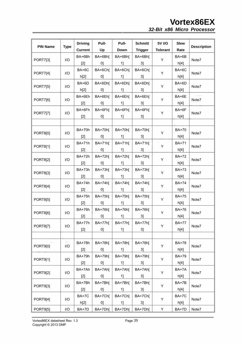
Vortex86EX32-Bit x86 Micro Processor
Vortex86EX datasheet Rev. 1.3 Page 39Copyright © 2013 DMP
PIN Name TypeDriving
Current
Pull-
Up
Pull-
Down
Schmitt
Trigger
5V I/O
Tolerant
Slew
Rate Description
PORT7[3] I/O BA+6Bh
[2]
BA+6Bh[
0]
BA+6Bh[
1]
BA+6Bh[
3] Y
BA+6B
h[4] Note7
PORT7[4] I/O BA+6C
h[2]
BA+6Ch[
0]
BA+6Ch[
1]
BA+6Ch[
3] Y
BA+6C
h[4] Note7
PORT7[5] I/O BA+6D
h[2]
BA+6Dh[
0]
BA+6Dh[
1]
BA+6Dh[
3] Y
BA+6D
h[4] Note7
PORT7[6] I/O BA+6Eh
[2]
BA+6Eh[
0]
BA+6Eh[
1]
BA+6Eh[
3] Y
BA+6E
h[4] Note7
PORT7[7] I/O BA+6Fh
[2]
BA+6Fh[
0]
BA+6Fh[
1]
BA+6Fh[
3] Y
BA+6F
h[4] Note7
PORT8[0] I/O BA+70h
[2]
BA+70h[
0]
BA+70h[
1]
BA+70h[
3] Y
BA+70
h[4] Note7
PORT8[1] I/O BA+71h
[2]
BA+71h[
0]
BA+71h[
1]
BA+71h[
3] Y
BA+71
h[4] Note7
PORT8[2] I/O BA+72h
[2]
BA+72h[
0]
BA+72h[
1]
BA+72h[
3] Y
BA+72
h[4] Note7
PORT8[3] I/O BA+73h
[2]
BA+73h[
0]
BA+73h[
1]
BA+73h[
3] Y
BA+73
h[4] Note7
PORT8[4] I/O BA+74h
[2]
BA+74h[
0]
BA+74h[
1]
BA+74h[
3] Y
BA+74
h[4] Note7
PORT8[5] I/O BA+75h
[2]
BA+75h[
0]
BA+75h[
1]
BA+75h[
3] Y
BA+75
h[4] Note7
PORT8[6] I/O BA+76h
[2]
BA+76h[
0]
BA+76h[
1]
BA+76h[
3] Y
BA+76
h[4] Note7
PORT8[7] I/O BA+77h
[2]
BA+77h[
0]
BA+77h[
1]
BA+77h[
3] Y
BA+77
h[4] Note7
PORT9[0] I/O BA+78h
[2]
BA+78h[
0]
BA+78h[
1]
BA+78h[
3] Y
BA+78
h[4] Note7
PORT9[1] I/O BA+79h
[2]
BA+79h[
0]
BA+79h[
1]
BA+79h[
3] Y
BA+79
h[4] Note7
PORT9[2] I/O BA+7Ah
[2]
BA+7Ah[
0]
BA+7Ah[
1]
BA+7Ah[
3] Y
BA+7A
h[4] Note7
PORT9[3] I/O BA+7Bh
[2]
BA+7Bh[
0]
BA+7Bh[
1]
BA+7Bh[
3] Y
BA+7B
h[4] Note7
PORT9[4] I/O BA+7C
h[2]
BA+7Ch[
0]
BA+7Ch[
1]
BA+7Ch[
3] Y
BA+7C
h[4] Note7
PORT9[5] I/O BA+7D BA+7Dh[ BA+7Dh[ BA+7Dh[ Y BA+7D Note7

Vortex86EX32-Bit x86 Micro Processor
Vortex86EX datasheet Rev. 1.3 Page 40Copyright © 2013 DMP
PIN Name TypeDriving
Current
Pull-
Up
Pull-
Down
Schmitt
Trigger
5V I/O
Tolerant
Slew
Rate Description
h[2] 0] 1] 3] h[4]
PORT9[6] I/O BA+7Eh
[2]
BA+7Eh[
0]
BA+7Eh[
1]
BA+7Eh[
3] Y
BA+7E
h[4] Note7
PORT9[7] I/O BA+7Fh
[2]
BA+7Fh[
0]
BA+7Fh[
1]
BA+7Fh[
3] Y
BA+7F
h[4] Note7
Definition: --: Not need to specify Y: Yes F: Fast S: Slow The pull-up/pull-down resistance is 75KΩ Note1: USB analog IO pad Note2: A PCI type IO pad. Note3: define by North Function1 84h. Note4: USB analog IO pad Note5: BIAS external resistor connecting pin Note6: Externel Phy test pin Note7: BA (Base Address) defined on South Bridge Function PCI config 65-64h, pPORT0~9 setting depend on recommend multi-function Pin Pull-up/Down list Note8: Programmable through South config register 48h
4.7 The Registers only reset by power-good
These registers are only reset by PowerGood 1. GPIO_0~9 Direction register 2. GPIO_0~9 Data register 3. GPIO Port Config Registers 4. WatchDog Timer_0 3Ch Indirect access register 5. WatchDog Timer_1 ADh register

Vortex86EX32-Bit x86 Micro Processor
Vortex86EX datasheet Rev. 1.3 Page 41Copyright © 2013 DMP
5. System Address Map
The SoC supports 4 Gbytes of addressable memory space and 64 Kbytes of addressable I/O space.
In order to be compatible with PC/AT system, the lower 1 Mbytes of this addressable memory is
divided into regions which can be individually controlled with programmable attributes such as
disable, read/write, write only, or read only (see Chapter 11, Register Description section for details
on attribute programming).
5.1 Memory Address Ranges
Figure 5-1 represents SoC memory address map. It shows the main memory regions defined and
supported by the SoC. At the highest level, the address space is divided into two main conceptual
regions. One is the 0–1-Mbyte DOS compatibility region and the other is 1-Mbyte to 4-Gbyte
extended memory region. The SoC supports several main memory sizes (reference 10.4). The main
memory type and size in the system will be auto-detected by the system BIOS.
Figure 5-1. Memory Address Map
Vortex86EX32-Bit x86 Micro Processor
Vortex86EX datasheet Rev. 1.3 Page 42Copyright © 2013 DMP
5.1.1 Dos Compatibility Region
The first region of memory is called the Dos Compatibility Region because it is defined for early PC.
This area is divided into the following address regions:
0–640-Kbyte DOS Area
640–768-Kbyte Video Buffer Area
768–896-Kbyte in 16-Kbyte sections (total of 8 sections) - Expansion Area
896–960-Kbyte in 16-Kbyte sections (total of 4 sections) - Extended System BIOS Area
960-Kbyte–1-Mbyte Memory (BIOS Area) - System BIOS Area
From 640 Kbytes – 1Mbytes: it can be divided into fourteen ranges which can be enabled or
disabled independently for both read and write. These regions can also be mapped to either main
DRAM or PCI by system BIOS. (See A/B Page control Register and Memory Attribute Register in
Section 3, Chapter 11.)
DOS Area (00000–9FFFFh)
The DOS area (00000h – 9FFFFh) is 640 Kbytes in size. It is always mapped to the main memory
controlled by the SoC.
Video Buffer Area (A0000–BFFFFh)
The 128-Kbyte graphics adapter memory region is normally mapped to a video device on the PCI
bus (typically VGA controller). This area is controlled by the A/B Page control Register. It can be
mapped to either main DRAM or PCI for both read and write command.
ISA Expansion Area (C0000–DFFFFh)
This 128-Kbyte ISA Expansion region is divided into eight 16-Kbyte segments. Each segment can
be assigned one of four Read/Write states: read-only, write-only, read/write, or disabled. Typically,
these blocks are mapped through the PCI bridge to ISA space. Memory that is disabled is not
remapped.
Extended System BIOS Area (E0000–EFFFFh)
This 64-Kbyte area is divided into four 16-Kbyte segments. Each segment can be assigned
independent read and write attributes so it can be mapped either to main DRAM or to PCI. Typically,
this area is used for RAM or ROM. Memory that is disabled is not remapped.
System BIOS Area (F0000–FFFFFh)
This area is a single 64-Kbyte segment that can be assigned read and write attributes. It is by
default (after reset) read/write disabled and cycles are forwarded to PCI. By manipulating the
read/write attributes, the SoC can “shadow” BIOS into main memory. Memory that is disabled is not
Vortex86EX32-Bit x86 Micro Processor
Vortex86EX datasheet Rev. 1.3 Page 43Copyright © 2013 DMP
remapped.
5.1.2 Extended Memory Region
This memory region covers 10_0000h (1 Mbytes) to FFFF_FFFFh (4 Gbytes minus 1) address
range and is divided into the following regions:
DRAM memory from 1 Mbytes to a top of memory
PCI Memory space from the top of memory to 4 Gbytes
High BIOS area from 4 Gbytes to 4 Gbytes minus 16 Mbytes
Main DRAM Address Range (0010_0000h to Top of Main Memory)
The address range from 1 Mbytes to the top of main memory is mapped to the main memory
address range controlled by the SoC. All accesses to addresses within this range are forwarded to
the main memory.
PCI Memory Address Range (Top of Main Memory to 4 Gbytes)
The address range from the top of main DRAM to 4 Gbytes is normally mapped to PCI. The PMC
forwards all accesses within this address range to PCI.
1. High BIOS Area (FF00_0000–FFFF_FFFFh)
The top 16 Mbytes of the Extended Memory Region is reserved for System BIOS (High BIOS),
extended BIOS for PCI devices, and the A20 alias of the system BIOS. The CPU begins execution
from the High BIOS after reset. This region is mapped to the PCI so that the upper subset of this
region is aliased to 16 Mbytes minus 256 Kbytes range. The actual address space required for the
BIOS is less than 2 Mbytes.
Vortex86EX32-Bit x86 Micro Processor
Vortex86EX datasheet Rev. 1.3 Page 44Copyright © 2013 DMP
5.2 Memory Shadowing
Any block of memory that can be designated as read only or write only can be “shadowed” into
PMC DRAM memory. Typically, this is done to allow ROM code to execute more rapidly out of main
DRAM. ROM is used as read only during the copy process while DRAM at the same time is
designated write only. After copying, the DRAM is designated read only so that ROM is shadowed.
CPU bus transactions are routed accordingly. The PMC does not respond to transactions originating
from PCI or ISA masters and targeted at shadowed memory blocks.
5.3 I / O Address Space
The SoC positively decodes accesses to all internal registers, including PCI configuration registers
(CF8h and CFCh), PC/AT Compatible IO registers (8237, 8254 & 8259), and all relocatable IO
space registers (UART).
Vortex86EX32-Bit x86 Micro Processor
Vortex86EX datasheet Rev. 1.3 Page 45Copyright © 2013 DMP
6. Operation Mode
The SoC supports three operation modes: protected mode, real-address mode and flat mode. The
operation mode determines which instructions and architectural features are accessible:
Protected mode. In this mode all instructions and architectural features are available,
providing the highest performance and capability. This is the recommended mode for all new
applications and operating systems.
Among the capabilities of protected mode is the ability to directly execute “real-address mode” 8086
software in a protected, multitasking environment. This feature is called virtual-8086 mode, although
it is not actually a processor mode. Virtual-8086 mode is actually a protected mode attribute that
can be enabled for any task.
Real-address mode. It provides the programming environment of the 8086 processor
with a few extensions (such as the ability to switch to protected or system management mode). The
processor is placed in real-address mode following power-up or a reset.
Flat mode. In general, this mode is similar with Real-Address mode. But there is one
difference involved, i.e. Flat mode can access 4GBytes address.
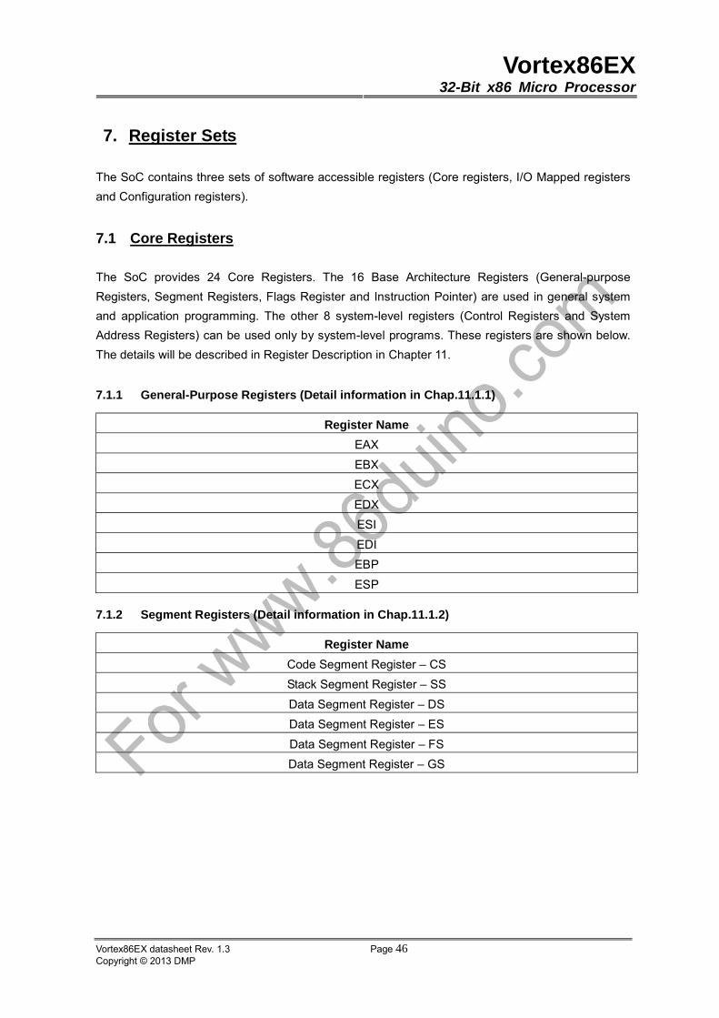
Vortex86EX32-Bit x86 Micro Processor
Vortex86EX datasheet Rev. 1.3 Page 46Copyright © 2013 DMP
7. Register Sets
The SoC contains three sets of software accessible registers (Core registers, I/O Mapped registers
and Configuration registers).
7.1 Core Registers
The SoC provides 24 Core Registers. The 16 Base Architecture Registers (General-purpose
Registers, Segment Registers, Flags Register and Instruction Pointer) are used in general system
and application programming. The other 8 system-level registers (Control Registers and System
Address Registers) can be used only by system-level programs. These registers are shown below.
The details will be described in Register Description in Chapter 11.
7.1.1 General-Purpose Registers (Detail information in Chap.11.1.1)
Register Name
EAX
EBX
ECX
EDX
ESI
EDI
EBP
ESP
7.1.2 Segment Registers (Detail information in Chap.11.1.2)
Register Name
Code Segment Register – CS
Stack Segment Register – SS
Data Segment Register – DS
Data Segment Register – ES
Data Segment Register – FS
Data Segment Register – GS
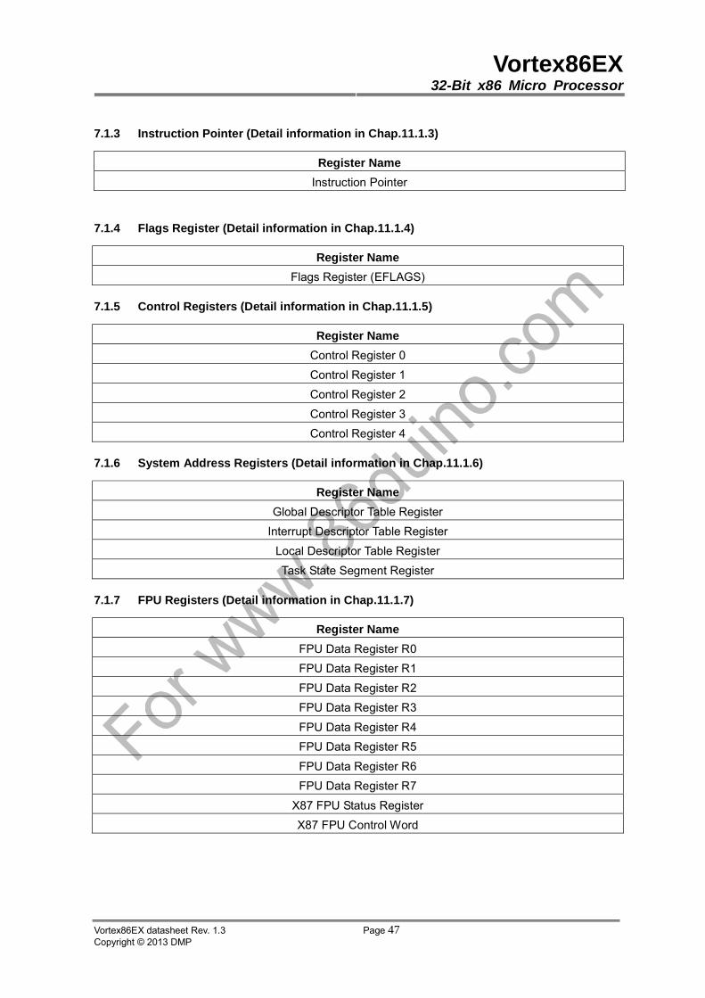
Vortex86EX32-Bit x86 Micro Processor
Vortex86EX datasheet Rev. 1.3 Page 47Copyright © 2013 DMP
7.1.3 Instruction Pointer (Detail information in Chap.11.1.3)
Register Name
Instruction Pointer
7.1.4 Flags Register (Detail information in Chap.11.1.4)
Register Name
Flags Register (EFLAGS)
7.1.5 Control Registers (Detail information in Chap.11.1.5)
Register Name
Control Register 0
Control Register 1
Control Register 2
Control Register 3
Control Register 4
7.1.6 System Address Registers (Detail information in Chap.11.1.6)
Register Name
Global Descriptor Table Register
Interrupt Descriptor Table Register
Local Descriptor Table Register
Task State Segment Register
7.1.7 FPU Registers (Detail information in Chap.11.1.7)
Register Name
FPU Data Register R0
FPU Data Register R1
FPU Data Register R2
FPU Data Register R3
FPU Data Register R4
FPU Data Register R5
FPU Data Register R6
FPU Data Register R7
X87 FPU Status Register
X87 FPU Control Word
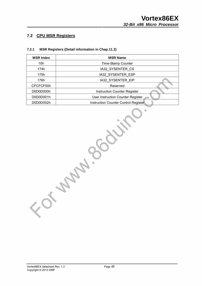
Vortex86EX32-Bit x86 Micro Processor
Vortex86EX datasheet Rev. 1.3 Page 48Copyright © 2013 DMP
7.2 CPU MSR Registers
7.2.1 MSR Registers (Detail information in Chap.11.2)
MSR Index MSR Name
10h Time-Stamp Counter
174h IA32_SYSENTER_CS
175h IA32_SYSENTER_ESP
176h IA32_SYSENTER_EIP
CFCFCF00h Reserved
D0D0D000h Instruction Counter Register
D0D0D001h User Instruction Counter Register
D0D0D002h Instruction Counter Control Register

Vortex86EX32-Bit x86 Micro Processor
Vortex86EX datasheet Rev. 1.3 Page 49Copyright © 2013 DMP
7.3 I / O Mapped Registers
The I/O Mapped Registers are usually used to control the SoC integrated peripherals or to store the
peripherals’ data, addresses and statuses. We divided these I/O Mapped Registers into fourteen
subsets, including PCI Configurations Registers, Slave DMA Controller Registers, DMA Page
Registers, Master DMA Controller Registers, DMA High Page Registers, Timer / Counter
Registers, Interrupt Edge/Level Control Registers, NMI Status and Control Register, CMOS
Memory & RTC Registers, System Control Register and Serial Port Registers. These registers
have fixed IO Address except Serial Port Registers.
The base address of Serial Port Registers is programmable via the Internal UART IO Address
Register in Vortex86EX_SB Configuration Space Register.
These registers are listed as below. In Chapter 11, Register Description will show more detailed
information about these registers.
7.3.1 PCI Configuration Registers (Detail information in Chap.11.3.1)
IO Address Register Name
0CFBh-0CF8h PCI Configuration Address Register
0CFFh-0CFCh PCI Configuration Data Register
7.3.2 Slave DMA Controller Registers(Detail information in Chap.11.3.2)
IO Address Register Name
00h Slave DMA Channel 0 Base/Current Address Register
01h Slave DMA Channel 0 Base/Current Count Register
02h Slave DMA Channel 1 Base/Current Address Register
03h Slave DMA Channel 1 Base/Current Count Register
04h Slave DMA Channel 2 Base/Current Address Register
05h Slave DMA Channel 2 Base/Current Count Register
06h Slave DMA Channel 3 Base/Current Address Register
07h Slave DMA Channel 3 Base/Current Count Register
08h Slave DMA Command/Status Register
09h Slave DMA Command/Request Register
0Ah Slave DMA Command/Single Mask Register
0Bh Slave DMA Mode Register
0Ch Slave DMA Set/Clear First/Last Clear F/F Register
0Dh Slave DMA Temporary/Master Disable Register
0Eh Slave DMA Clear Mask/Mode register pointer Register
0Fh Slave DMA Write Mask Register
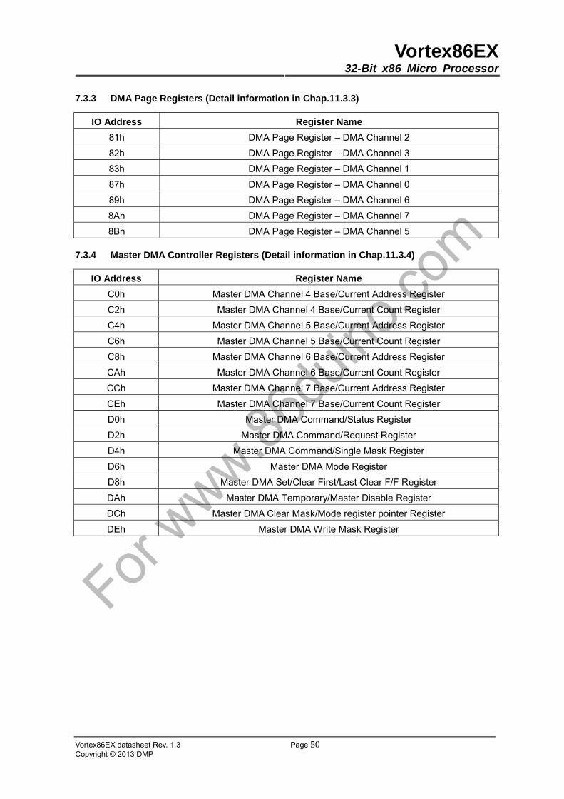
Vortex86EX32-Bit x86 Micro Processor
Vortex86EX datasheet Rev. 1.3 Page 50Copyright © 2013 DMP
7.3.3 DMA Page Registers (Detail information in Chap.11.3.3)
IO Address Register Name
81h DMA Page Register – DMA Channel 2
82h DMA Page Register – DMA Channel 3
83h DMA Page Register – DMA Channel 1
87h DMA Page Register – DMA Channel 0
89h DMA Page Register – DMA Channel 6
8Ah DMA Page Register – DMA Channel 7
8Bh DMA Page Register – DMA Channel 5
7.3.4 Master DMA Controller Registers (Detail information in Chap.11.3.4)
IO Address Register Name
C0h Master DMA Channel 4 Base/Current Address Register
C2h Master DMA Channel 4 Base/Current Count Register
C4h Master DMA Channel 5 Base/Current Address Register
C6h Master DMA Channel 5 Base/Current Count Register
C8h Master DMA Channel 6 Base/Current Address Register
CAh Master DMA Channel 6 Base/Current Count Register
CCh Master DMA Channel 7 Base/Current Address Register
CEh Master DMA Channel 7 Base/Current Count Register
D0h Master DMA Command/Status Register
D2h Master DMA Command/Request Register
D4h Master DMA Command/Single Mask Register
D6h Master DMA Mode Register
D8h Master DMA Set/Clear First/Last Clear F/F Register
DAh Master DMA Temporary/Master Disable Register
DCh Master DMA Clear Mask/Mode register pointer Register
DEh Master DMA Write Mask Register

Vortex86EX32-Bit x86 Micro Processor
Vortex86EX datasheet Rev. 1.3 Page 51Copyright © 2013 DMP
7.3.5 DMA High Page Registers (Detail information in Chap.11.3.5)
7.3.6 Timer / Counter Registers (Detail information in Chap.11.3.6)
7.3.7 Indirect Access Registers (Detail information in Chap.11.3.7)
7.3.8 Master Interrupt Controller Registers (Detail information in Chap.11.3.8)
7.3.9 Slave Interrupt Controller Registers (Detail information in Chap.11.3.9)
IO Address Register Name
481h DMA High Page Register – DMA Channel 2.
482h DMA High Page Register – DMA Channel 3.
483h DMA High Page Register – DMA Channel 1.
487h DMA High Page Register – DMA Channel 0.
489h DMA High Page Register – DMA Channel 6.
48Ah DMA High Page Register – DMA Channel 7.
48Bh DMA High Page Register – DMA Channel 5.
IO Address Register Name
40h Timer / Counter 0 Count Register
41h Timer / Counter 1 Count Register
42h Timer / Counter 2 Count Register
43h Timer / Counter Control Register
IO Address Register Name
22h Address Index Register for indirect access GPIO & WDT0
23h Data Register for indirect access GPIO & WDT0
IO Address Register Name
20h Master Interrupt Request/Interrupt Service/Interrupt Command Register
21h Master Interrupt Mask Register
IO Address Register Name
A0h Slave Interrupt Request/Interrupt Service/Interrupt Command Register
A1h Slave Interrupt Mask Register
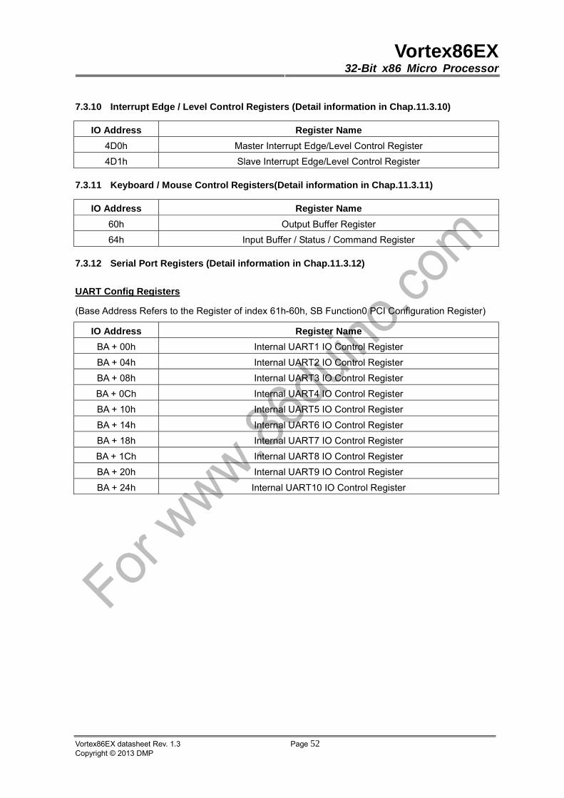
Vortex86EX32-Bit x86 Micro Processor
Vortex86EX datasheet Rev. 1.3 Page 52Copyright © 2013 DMP
7.3.10 Interrupt Edge / Level Control Registers (Detail information in Chap.11.3.10)
7.3.11 Keyboard / Mouse Control Registers(Detail information in Chap.11.3.11)
7.3.12 Serial Port Registers (Detail information in Chap.11.3.12)
UART Config Registers
(Base Address Refers to the Register of index 61h-60h, SB Function0 PCI Configuration Register)
IO Address Register Name
4D0h Master Interrupt Edge/Level Control Register
4D1h Slave Interrupt Edge/Level Control Register
IO Address Register Name
60h Output Buffer Register
64h Input Buffer / Status / Command Register
IO Address Register Name
BA + 00h Internal UART1 IO Control Register
BA + 04h Internal UART2 IO Control Register
BA + 08h Internal UART3 IO Control Register
BA + 0Ch Internal UART4 IO Control Register
BA + 10h Internal UART5 IO Control Register
BA + 14h Internal UART6 IO Control Register
BA + 18h Internal UART7 IO Control Register
BA + 1Ch Internal UART8 IO Control Register
BA + 20h Internal UART9 IO Control Register
BA + 24h Internal UART10 IO Control Register

Vortex86EX32-Bit x86 Micro Processor
Vortex86EX datasheet Rev. 1.3 Page 53Copyright © 2013 DMP
Serial Port Registers
(UART1 Base Address Refers to UART Config Register Offset 00h)
(UART2 Base Address Refers to UART Config Register Offset 04h)
(UART3 Base Address Refers to UART Config Register Offset 08h)
(UART4 Base Address Refers to UART Config Register Offset 0Ch)
(UART5 Base Address Refers to UART Config Register Offset 10h)
(UART6 Base Address Refers to UART Config Register Offset 14h)
(UART7 Base Address Refers to UART Config Register Offset 18h)
(UART8 Base Address Refers to UART Config Register Offset 1Ch)
(UART9 Base Address Refers to UART Config Register Offset 20h)
(UART10 Base Address Refers to UART Config Register Offset 24h)
UART Global Interrupt Status
(Base Address defined on SB Function 1 PCI CFG 81- 80h)
IO Address Register Name
BA + 0h Transmit/Receive Data Buffer (DLAB=0)
BA + 0h LSB of Baud Rate Generator Divisor Latches (DLAB=1)
BA + 1h Interrupt Enable Register (DLAB=0)
BA + 1h MSB of Baud Rate Generator Divisor Latches (DLAB=1)
BA + 2h Interrupt Identification Register
BA + 2h FIFO Control Register
BA + 3h Line Control Register
BA + 4h Modem Control Register
BA + 5h Line Status Register
BA + 6h Modem Status Register
BA + 7h Scratchpad Register
IO Address Register Name
BA + 0h UART Global Interrupt Status Register
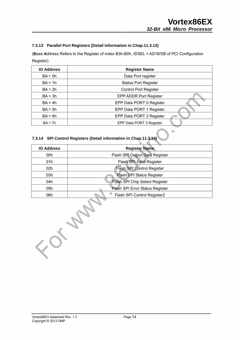
Vortex86EX32-Bit x86 Micro Processor
Vortex86EX datasheet Rev. 1.3 Page 54Copyright © 2013 DMP
7.3.13 Parallel Port Registers (Detail information in Chap.11.3.13)
(Base Address Refers to the Register of index B3h-B0h, IDSEL = AD18/SB of PCI Configuration
Register)
7.3.14 SPI Control Registers (Detail information in Chap.11.3.14)
IO Address Register Name
BA + 0h Data Port register
BA + 1h Status Port Register
BA + 2h Control Port Register
BA + 3h EPP ADDR Port Register
BA + 4h EPP Data PORT 0 Register
BA + 5h EPP Data PORT 1 Register
BA + 6h EPP Data PORT 2 Register
BA + 7h EPP Data PORT 3 Register
IO Address Register Name
00h Flash SPI Output Data Register
01h Flash SPI Input Register
02h Flash SPI Control Register
03h Flash SPI Status Register
04h Flash SPI Chip Select Register
05h Flash SPI Error Status Register
06h Flash SPI Control Register2
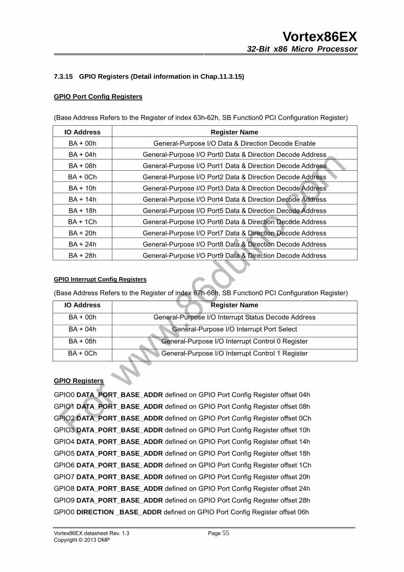
Vortex86EX32-Bit x86 Micro Processor
Vortex86EX datasheet Rev. 1.3 Page 55Copyright © 2013 DMP
7.3.15 GPIO Registers (Detail information in Chap.11.3.15)
GPIO Port Config Registers
(Base Address Refers to the Register of index 63h-62h, SB Function0 PCI Configuration Register)
GPIO Interrupt Config Registers
(Base Address Refers to the Register of index 67h-66h, SB Function0 PCI Configuration Register)
GPIO Registers
GPIO0 DATA_PORT_BASE_ADDR defined on GPIO Port Config Register offset 04h
GPIO1 DATA_PORT_BASE_ADDR defined on GPIO Port Config Register offset 08h
GPIO2 DATA_PORT_BASE_ADDR defined on GPIO Port Config Register offset 0Ch
GPIO3 DATA_PORT_BASE_ADDR defined on GPIO Port Config Register offset 10h
GPIO4 DATA_PORT_BASE_ADDR defined on GPIO Port Config Register offset 14h
GPIO5 DATA_PORT_BASE_ADDR defined on GPIO Port Config Register offset 18h
GPIO6 DATA_PORT_BASE_ADDR defined on GPIO Port Config Register offset 1Ch
GPIO7 DATA_PORT_BASE_ADDR defined on GPIO Port Config Register offset 20h
GPIO8 DATA_PORT_BASE_ADDR defined on GPIO Port Config Register offset 24h
GPIO9 DATA_PORT_BASE_ADDR defined on GPIO Port Config Register offset 28h
GPIO0 DIRECTION _BASE_ADDR defined on GPIO Port Config Register offset 06h
IO Address Register Name
BA + 00h General-Purpose I/O Data & Direction Decode Enable
BA + 04h General-Purpose I/O Port0 Data & Direction Decode Address
BA + 08h General-Purpose I/O Port1 Data & Direction Decode Address
BA + 0Ch General-Purpose I/O Port2 Data & Direction Decode Address
BA + 10h General-Purpose I/O Port3 Data & Direction Decode Address
BA + 14h General-Purpose I/O Port4 Data & Direction Decode Address
BA + 18h General-Purpose I/O Port5 Data & Direction Decode Address
BA + 1Ch General-Purpose I/O Port6 Data & Direction Decode Address
BA + 20h General-Purpose I/O Port7 Data & Direction Decode Address
BA + 24h General-Purpose I/O Port8 Data & Direction Decode Address
BA + 28h General-Purpose I/O Port9 Data & Direction Decode Address
IO Address Register Name
BA + 00h General-Purpose I/O Interrupt Status Decode Address
BA + 04h General-Purpose I/O Interrupt Port Select
BA + 08h General-Purpose I/O Interrupt Control 0 Register
BA + 0Ch General-Purpose I/O Interrupt Control 1 Register

Vortex86EX32-Bit x86 Micro Processor
Vortex86EX datasheet Rev. 1.3 Page 56Copyright © 2013 DMP
GPIO1 DIRECTION _BASE_ADDR defined on GPIO Port Config Register offset 0Ah
GPIO2 DIRECTION _BASE_ADDR defined on GPIO Port Config Register offset 0Eh
GPIO3 DIRECTION _BASE_ADDR defined on GPIO Port Config Register offset 12h
GPIO4 DIRECTION _BASE_ADDR defined on GPIO Port Config Register offset 16h
GPIO5 DIRECTION _BASE_ADDR defined on GPIO Port Config Register offset 1Ah
GPIO6 DIRECTION _BASE_ADDR defined on GPIO Port Config Register offset 1Eh
GPIO7 DIRECTION _BASE_ADDR defined on GPIO Port Config Register offset 22h
GPIO8 DIRECTION _BASE_ADDR defined on GPIO Port Config Register offset 26h
GPIO9 DIRECTION _BASE_ADDR defined on GPIO Port Config Register offset 2Ah
GPIO Interrupt Status 0-1 _BASE_ADDR defined on GPIO Interrupt Config Register offset 00h
7.3.16 NMI Status and Control Register (Detail information in Chap.11.3.16)
7.3.17 WDT Registers (Detail information in Chap.11.3.17)
WDT1 Control Register
IO Address Register Name
BA + 00h GPIO PORT0 Data Register
BA + 00h GPIO PORT1 Data Register
BA + 00h GPIO PORT2 Data Register
BA + 00h GPIO PORT3 Data Register
BA + 00h GPIO PORT4 Data Register
BA + 00h GPIO PORT5 Data Register
BA + 00h GPIO PORT6 Data Register
BA + 00h GPIO PORT7 Data Register
BA + 00h GPIO PORT8 Data Register
BA + 00h GPIO PORT9 Data Register
BA + 00h GPIO PORT0 Direction Register
BA + 00h GPIO PORT1 Direction Register
BA + 00h GPIO PORT2 Direction Register
BA + 00h GPIO PORT3 Direction Register
BA + 00h GPIO PORT4 Direction Register
BA + 00h GPIO PORT5 Direction Register
BA + 00h GPIO PORT6 Direction Register
BA + 00h GPIO PORT7 Direction Register
BA + 00h GPIO PORT8 Direction Register
BA + 00h GPIO PORT9 Direction Register
BA + 00h GPIO Interrupt Status 0 Register
BA + 01h GPIO Interrupt Status 1 Register
IO Address Register Name
61h NMI Status and Control Register
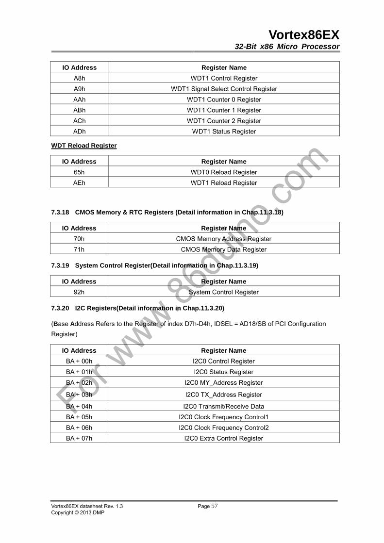
Vortex86EX32-Bit x86 Micro Processor
Vortex86EX datasheet Rev. 1.3 Page 57Copyright © 2013 DMP
WDT Reload Register
7.3.18 CMOS Memory & RTC Registers (Detail information in Chap.11.3.18)
7.3.19 System Control Register(Detail information in Chap.11.3.19)
7.3.20 I2C Registers(Detail information in Chap.11.3.20)
(Base Address Refers to the Register of index D7h-D4h, IDSEL = AD18/SB of PCI Configuration
Register)
IO Address Register Name
A8h WDT1 Control Register
A9h WDT1 Signal Select Control Register
AAh WDT1 Counter 0 Register
ABh WDT1 Counter 1 Register
ACh WDT1 Counter 2 Register
ADh WDT1 Status Register
IO Address Register Name
65h WDT0 Reload Register
AEh WDT1 Reload Register
IO Address Register Name
70h CMOS Memory Address Register
71h CMOS Memory Data Register
IO Address Register Name
92h System Control Register
IO Address Register Name
BA + 00h I2C0 Control Register
BA + 01h I2C0 Status Register
BA + 02h I2C0 MY_Address Register
BA + 03h I2C0 TX_Address Register
BA + 04h I2C0 Transmit/Receive Data
BA + 05h I2C0 Clock Frequency Control1
BA + 06h I2C0 Clock Frequency Control2
BA + 07h I2C0 Extra Control Register

Vortex86EX32-Bit x86 Micro Processor
Vortex86EX datasheet Rev. 1.3 Page 58Copyright © 2013 DMP
7.3.21 DOS 4Gpage Access Registers(Detail information in Chap.11.3.21)
7.3.22 Spare Registers(Detail information in Chap.11.3.22)
7.3.23 SMM Registers(Detail information in Chap.11.3.23)
(Base Address Refers to the Register of index 4Dh-4Ch, IDSEL = AD18/SB of PCI Configuration
Register)
IO Address Register Name
E3h – E0h D4GA1 Control and Source Address Register
E7h – E4h D4GA1 Destination Address Register
EBh – E8h D4GA2 Control and Source Address Register
EFh – ECh D4GA2 Destination Address Register
IO Address Register Name
80h Spare Register
84h Spare Register
85h Spare Register
86h Spare Register
88h Spare Register
8Ch Spare Register
8Dh Spare Register
8Eh Spare Register
8Fh Spare Register
480h Spare Register
484h Spare Register
485h Spare Register
486h Spare Register
488h Spare Register
48Ch Spare Register
48Dh Spare Register
48Eh Spare Register
48Fh Spare Register
IO Address Register Name
B2h Software SMI Trigger Port2
IO Address Register Name
BA + 00h SMI Event Status Register
BA + 04h SMI Event Control Register
BA + 08h SMI function Control
BA + 09h SMM Status
BA + 0Ah Software SMI Trigger Port1

Vortex86EX32-Bit x86 Micro Processor
Vortex86EX datasheet Rev. 1.3 Page 59Copyright © 2013 DMP
7.3.24 Fast Ethernet MAC Registers(Detail information in Chap.14.7)
(Base Address Refers to the Register of index 10h/14h, Device 8 of PCI Configuration Register)
IO Address Register Name
BA + 00h MAC Control Register 0
BA + 04h MAC Control Register 1
BA + 08h MAC Bus Control Register
BA + 0Ch MAC TX Interrupt Control Register
BA + 10h MAC RX Interrupt Control Register
BA + 14h MAC TX Poll Command Register
BA + 18h MAC RX Buffer Size Register
BA + 1Ah MAC RX Descriptor Control Register
BA + 1Ch MAC Last Status Register
BA + 20h MAC MDIO Control Register
BA + 24h MAC MDIO Read Data Register
BA + 28h MAC MDIO Write Data Register
BA + 2Ch MAC TX Descriptor Start Address 0 Register
BA + 30h MAC TX Descriptor Start Address 1 Register
BA + 34h MAC RX Descriptor Start Address 0 Register
BA + 38h MAC RX Descriptor Start Address 1 Register
BA + 3Ch MAC INT Status Register
BA + 40h MAC INT Enable Register
BA + 44h MAC Event Counter INT Status Register
BA + 48h MAC Event Counter INT Enable Register
BA + 50h MAC Successfully Received Packet Counter Register
BA + 52h MAC Event Counter 0 Register
BA + 54h MAC Event Counter 1 Register
BA + 56h MAC Event Counter 2 Register
BA + 58h MAC Event Counter 3 Register
BA + 5Ah MAC Successfully Transmit Packet Counter Register
BA + 5Ch MAC Event Counter 4 Register
BA + 5Eh MAC Pause Frame Counter Register
BA + 60h MAC Hash Table Word 0
BA + 62h MAC Hash Table Word 1
BA + 64h MAC Hash Table Word 2
BA + 66h MAC Hash Table Word 3
BA + 68h MAC Multicast Address first two bytes Register
Vortex86EX32-Bit x86 Micro Processor
Vortex86EX datasheet Rev. 1.3 Page 60Copyright © 2013 DMP
BA + 6Ah MAC Multicast Address second two bytes Register
BA + 6Ch MAC Multicast Address last two bytes Register
BA + 70h MAC Multicast Address first two bytes Register
BA + 72h MAC Multicast Address second two bytes Register
BA + 74h MAC Multicast Address last two bytes Register
BA + 78h MAC Multicast Address first two bytes Register
BA + 7Ah MAC Multicast Address second two bytes Register
BA + 7Ch MAC Multicast Address last two bytes Register
BA + 80h MAC Multicast Address first two bytes Register
BA + 82h MAC Multicast Address second two bytes Register
BA + 84h MAC Multicast Address last two bytes Register
BA + 88h MAC PHY Status Change Configuration Register
BA + 8Ah MAC PHY Status Register
BA + 8Ch Phy Status Register 2
BA + ACh MAC Memory BIST Control Register
BA + B6h MDC Speed Control Register
BA + BCh MAC ID
Vortex86EX32-Bit x86 Micro Processor
Vortex86EX datasheet Rev. 1.3 Page 61Copyright © 2013 DMP
7.3.25 USB 1.1 OHCI Operation Registers(Detail information in Chap.12.3.2)
(OHCI1 Base Address Refers to the Register of index 10h, Device 10, Function 0 of PCI
Configuration Register)
IO Address Register Name
BA + 00h HC Revision Register
BA + 04h HC Control Register
BA + 08h HC Command Status Regster
BA + 0Ch HC Interrupt Status Regster
BA + 10h HC Interrupt Enable Regster
BA + 14h HC Interrupt Disable Register
BA + 18h HC HCCA Register
BA + 1Ch HC Period Current ED Regster
BA + 20h HC Control Head ED Regster
BA + 24h HC Control Current ED Register
BA + 28h HC Bulk Head ED Register
BA + 2Ch HC Bulk Current ED Register
BA + 30h HC Done Head Register
BA + 34h HC Fm Interval Register
BA + 38h HC Fm Remaining Register
BA + 3Ch HC Fm Number Register
BA + 40h HC Periodic Start Register
BA + 44h HC LS Threshold Register
BA + 48h HC Rh Descriptor A Register
BA + 4Ch HC Rh Descriptor B Register
BA + 50h HC Rh Status Register
BA + 54h HC Rh Port Status [1] Register
BA + 58h HC Rh PortStatus [2] Register
Vortex86EX32-Bit x86 Micro Processor
Vortex86EX datasheet Rev. 1.3 Page 62Copyright © 2013 DMP
7.3.26 USB 2.0 EHCI Operation Registers(Detail information in Chap.12.3.4)
(EHCI1 Base Address Refers to the Register of index 10h, Device 10, Function 1 of PCI
Configuration Register)
IO Address Register Name
BA + 00h Capability Register Length Register
BA + 03h – 02h Host Controller Interface Version Number
BA + 07h – 04h Structural Parameters Register
BA + 0Bh – 08h Capability Parameters Register
BA + 23h – 20h USB2.0 Command Register
BA + 27h – 24h USB2.0 Status Register
BA + 2Bh – 28h USB2.0 Interrupt Enable Register
BA + 2Fh – 2Ch USB2.0 Frame Index register
BA + 37h – 34h Periodic Frame List Base Address Register
BA + 3Bh – 38h Current Asynchronous List Address Register
BA + 63h – 60h Configured Flag Register
BA + 67h – 64h Port 0 Status and Control Register
BA + 6Bh – 68h Port 1 Status and Control Register
Vortex86EX32-Bit x86 Micro Processor
Vortex86EX datasheet Rev. 1.3 Page 63Copyright © 2013 DMP
7.3.27 USB Device Operation Registers(Detail information in Chap.15.4)
(Base Address Refers to the Register of index 10h, Device 15, Function 0 of PCI Configuration
Register)
IO Address Register Name
BA+ 00h USB device address register
BA + 02h Control function register
BA + 07h – 06h Frame number register
BA + 0Bh – 08h Interrupt enable register
BA + 0Fh – 0Ch Interrupt status register
BA + 10h Control endpoint 0 type register
BA + 12h OUT endpoint 1 type register
BA + 14h IN endpoint 1 type register
BA + 16h OUT endpoint 2 type register
BA + 18h IN endpoint 2 type register
BA + 1Ah OUT endpoint 3 type register
BA + 1Ch IN endpoint 3 type register
BA + 44h Endpoint 0 setup token transaction data buffer start address register
BA + 48h Endpoint 0 OUT token transaction data buffer start address register
BA + 4Ch Endpoint 0 IN token transaction data buffer start address register
BA + 50h Endpoint 1 OUT token transaction data buffer start address register
BA + 54h Endpoint 1 IN token transaction data buffer start address register
BA + 58h Endpoint 2 OUT token transaction data buffer start address register
BA + 5Ch Endpoint 2 IN token transaction data buffer start address register
BA + 60h Endpoint 3 OUT token transaction data buffer start address register
BA + 64h Endpoint 3 IN token transaction data buffer start address register
BA + 68h Test mode register
BA + 7Eh Interrupt configuration register

Vortex86EX32-Bit x86 Micro Processor
Vortex86EX datasheet Rev. 1.3 Page 64Copyright © 2013 DMP
7.3.28 SD/SATA Controller Registers(Detail information in Chap.13.7)
(Base Address1 Refers to the Register of index 10h, Device 12, Function 0 of PCI Configuration
Register)
(Base Address2 Refers to the Register of index 14h, Device 12, Function 0 of PCI Configuration
Register)
(Base Address3 Refers to the Register of index 18h, Device 12, Function 0 of PCI Configuration
Register)
(Base Address4 Refers to the Register of index 1Ch, Device 12, Function 0 of PCI Configuration
Register)
(Base Address5 Refers to the Register of index 20h, Device 12, Function 0 of PCI Configuration
Register)
IO Address Register Name
BA[1] + 00h Primary IDE Data Register
BA[1] + 01h Primary IDE Error/Feature Register
BA[1] + 02h Primary IDE Sector Count Register
BA[1] + 03h Primary IDE Sector Number Register
BA[1] + 04h Primary IDE Cylinder Low Register
BA[1] + 05h Primary IDE Cylinder High Register
BA[1] + 06h Primary IDE Device/Head Register
BA[1] + 07h Primary IDE Command/Status Register
BA[2] + 06h Primary IDE Device Control/Alternate Status Register
BA3 + 00h Secondary Data Register
BA3 + 01h Secondary IDE Error/Feature Register
BA3 + 02h Secondary IDE Sector Count Register
BA3 + 03h Secondary IDE Sector Number Register
BA3 + 04h Secondary IDE Cylinder Low Register
BA3 + 05h Secondary IDE Cylinder High Register
BA3 + 06h Secondary IDE Device/Head Register
BA3 + 07h Secondary IDE Command/Status Register
BA4 + 06h Secondary IDE Device Control/Alternate Status Register
BA5 + 01h - 00h Bus Master IDE Command Register for Primary Channel
BA5 + 03h - 02h Bus Master IDE Status Register for Primary Channel
BA5 + 07h – 04h Bus Master Descriptor Table Pointer Register for Primary ChanChannel
BA5 + 09h – 08h Bus Master IDE Command Register for Secondary Channel
BA5 + 0Bh – 0Ah Bus Master IDE Status Register for Secondary Channel
BA5 + 0Fh – 0Ch Bus Master Descriptor Table Pointer Register for Secondary ChanChannel
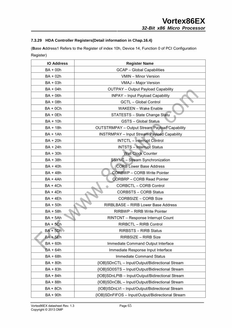
Vortex86EX32-Bit x86 Micro Processor
Vortex86EX datasheet Rev. 1.3 Page 65Copyright © 2013 DMP
7.3.29 HDA Controller Registers(Detail information in Chap.16.4)
(Base Address1 Refers to the Register of index 10h, Device 14, Function 0 of PCI Configuration
Register)
IO Address Register Name
BA + 00h GCAP – Global Capabilities
BA + 02h VMIN – Minor Version
BA + 03h VMAJ – Major Version
BA + 04h OUTPAY – Output Payload Capability
BA + 06h INPAY – Input Payload Capability
BA + 08h GCTL – Global Control
BA + 0Ch WAKEEN – Wake Enable
BA + 0Eh STATESTS – State Change Statu
BA + 10h GSTS – Global Status
BA + 18h OUTSTRMPAY – Output Stream Payload Capability
BA + 1Ah INSTRMPAY – Input Stream Payload Capability
BA + 20h INTCTL – Interrupt Control
BA + 24h INTSTS – Interrupt Status
BA + 30h Wall Clock Counter
BA + 38h SSYNC – Stream Synchronization
BA + 40h CORB Lower Base Address
BA + 48h CORBWP – CORB Write Pointer
BA + 4Ah CORBRP – CORB Read Pointer
BA + 4Ch CORBCTL – CORB Control
BA + 4Dh CORBSTS – CORB Status
BA + 4Eh CORBSIZE – CORB Size
BA + 50h RIRBLBASE – RIRB Lower Base Address
BA + 58h RIRBWP – RIRB Write Pointer
BA + 5Ah RINTCNT – Response Interrupt Count
BA + 5Ch RIRBCTL – RIRB Control
BA + 5Dh RIRBSTS – RIRB Status
BA + 5Eh RIRBSIZE – RIRB Size
BA + 60h Immediate Command Output Interface
BA + 64h Immediate Response Input Interface
BA + 68h Immediate Command Status
BA + 80h {IOB}SDnCTL – Input/Output/Bidirectional Stream
BA + 83h {IOB}SD0STS – Input/Output/Bidirectional Stream
BA + 84h {IOB}SDnLPIB – Input/Output/Bidirectional Stream
BA + 88h {IOB}SDnCBL – Input/Output/Bidirectional Stream
BA + 8Ch {IOB}ISDnLVI – Input/Output/Bidirectional Stream
BA + 90h {IOB}SDnFIFOS – Input/Output/Bidirectional Stream

Vortex86EX32-Bit x86 Micro Processor
Vortex86EX datasheet Rev. 1.3 Page 66Copyright © 2013 DMP
BA + 92h {IOB}SDnFMT – Input/Output/Bidirectional Stream
BA + 98h {IOB}SDnBDPL – Input/Output/Bidirectional Stream
7.3.30 ADC Registers(Detail information in Chap.11.3.24)
(ADC I/O Base Address Refers to the Register of index E1h-E0h, IDSEL = AD18/SB PCI Function 1
Configuration Register)
7.3.31 ACPI Registers (Detail information in Chap.11.3.25)
(ACPI I/O Base Address Refers to the Register of index F8h-F9h, IDSEL = AD18/SB PCI Function 0
Configuration Register)
IO Address Register Name
BA + 00h AUX Channel Select Register
BA + 01h ADC Control Register
BA + 02h ADC Status Register
BA + 03h ADC Data Register
IO Address Register Name
PMBASE+00h PM1 Status Register
PMBASE+02h PM1 Enable Register
PMBASE+04h PM1 Control Register
PMBASE+06h PM2 Control Register, Reserved now
PMBASE+08h Power Management Timer Register
PMBASE+10h Processor Control Register
PMBASE+14h Processor LVL2 Register
PMBASE+15h Processor LVL3 Register
PMBASE+20h General Purpose Status Register. Generate wakeup event
PMBASE+24h General Purpose Enable Register
PMBASE+28h General Purpose SMI Register
PMBASE+2Ch Global Status Register. Generate SMI event
PMBASE+30h Global Enable Register
PMBASE+34h Global Control Register
PMBASE+36h Software SMI Command Register
PMBASE+38h I/O Trap 1 Control Register
PMBASE+3Ch I/O Trap 2 Control Register
PMBASE+40h I/O Trap 3 Control Register
PMBASE+44h I/O Trap 4 Control Register
PMBASE+48h Trapped Status Register
PMBASE+4Ch Trapped Write Data Register
PMBASE+36h Software SMI Command Register
PMBASE+38h I/O Trap 1 Control Register
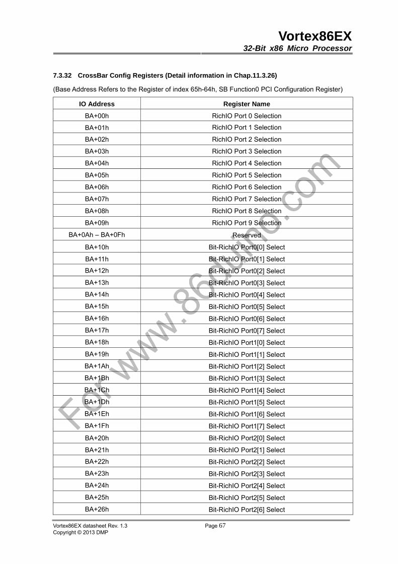
Vortex86EX32-Bit x86 Micro Processor
Vortex86EX datasheet Rev. 1.3 Page 67Copyright © 2013 DMP
7.3.32 CrossBar Config Registers (Detail information in Chap.11.3.26)
(Base Address Refers to the Register of index 65h-64h, SB Function0 PCI Configuration Register)
IO Address Register Name
BA+00h RichIO Port 0 Selection
BA+01h RichIO Port 1 Selection
BA+02h RichIO Port 2 Selection
BA+03h RichIO Port 3 Selection
BA+04h RichIO Port 4 Selection
BA+05h RichIO Port 5 Selection
BA+06h RichIO Port 6 Selection
BA+07h RichIO Port 7 Selection
BA+08h RichIO Port 8 Selection
BA+09h RichIO Port 9 Selection
BA+0Ah – BA+0Fh Reserved
BA+10h Bit-RichIO Port0[0] Select
BA+11h Bit-RichIO Port0[1] Select
BA+12h Bit-RichIO Port0[2] Select
BA+13h Bit-RichIO Port0[3] Select
BA+14h Bit-RichIO Port0[4] Select
BA+15h Bit-RichIO Port0[5] Select
BA+16h Bit-RichIO Port0[6] Select
BA+17h Bit-RichIO Port0[7] Select
BA+18h Bit-RichIO Port1[0] Select
BA+19h Bit-RichIO Port1[1] Select
BA+1Ah Bit-RichIO Port1[2] Select
BA+1Bh Bit-RichIO Port1[3] Select
BA+1Ch Bit-RichIO Port1[4] Select
BA+1Dh Bit-RichIO Port1[5] Select
BA+1Eh Bit-RichIO Port1[6] Select
BA+1Fh Bit-RichIO Port1[7] Select
BA+20h Bit-RichIO Port2[0] Select
BA+21h Bit-RichIO Port2[1] Select
BA+22h Bit-RichIO Port2[2] Select
BA+23h Bit-RichIO Port2[3] Select
BA+24h Bit-RichIO Port2[4] Select
BA+25h Bit-RichIO Port2[5] Select
BA+26h Bit-RichIO Port2[6] Select
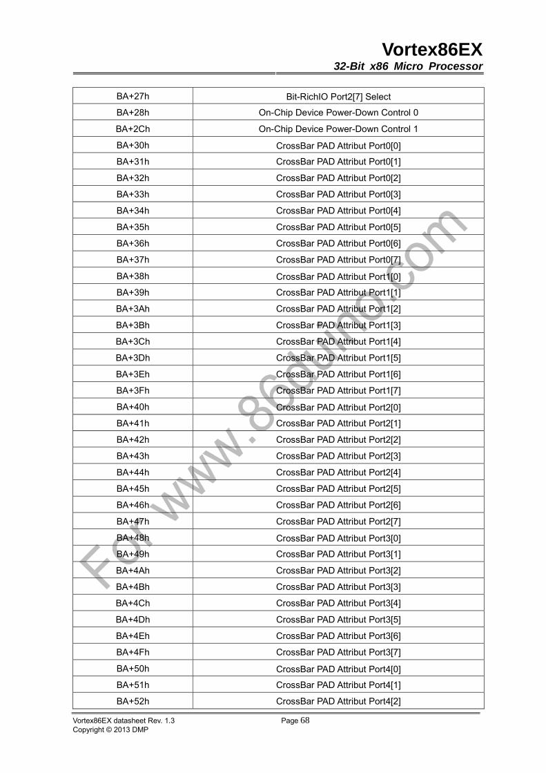
Vortex86EX32-Bit x86 Micro Processor
Vortex86EX datasheet Rev. 1.3 Page 68Copyright © 2013 DMP
BA+27h Bit-RichIO Port2[7] Select
BA+28h On-Chip Device Power-Down Control 0
BA+2Ch On-Chip Device Power-Down Control 1
BA+30h CrossBar PAD Attribut Port0[0]
BA+31h CrossBar PAD Attribut Port0[1]
BA+32h CrossBar PAD Attribut Port0[2]
BA+33h CrossBar PAD Attribut Port0[3]
BA+34h CrossBar PAD Attribut Port0[4]
BA+35h CrossBar PAD Attribut Port0[5]
BA+36h CrossBar PAD Attribut Port0[6]
BA+37h CrossBar PAD Attribut Port0[7]
BA+38h CrossBar PAD Attribut Port1[0]
BA+39h CrossBar PAD Attribut Port1[1]
BA+3Ah CrossBar PAD Attribut Port1[2]
BA+3Bh CrossBar PAD Attribut Port1[3]
BA+3Ch CrossBar PAD Attribut Port1[4]
BA+3Dh CrossBar PAD Attribut Port1[5]
BA+3Eh CrossBar PAD Attribut Port1[6]
BA+3Fh CrossBar PAD Attribut Port1[7]
BA+40h CrossBar PAD Attribut Port2[0]
BA+41h CrossBar PAD Attribut Port2[1]
BA+42h CrossBar PAD Attribut Port2[2]
BA+43h CrossBar PAD Attribut Port2[3]
BA+44h CrossBar PAD Attribut Port2[4]
BA+45h CrossBar PAD Attribut Port2[5]
BA+46h CrossBar PAD Attribut Port2[6]
BA+47h CrossBar PAD Attribut Port2[7]
BA+48h CrossBar PAD Attribut Port3[0]
BA+49h CrossBar PAD Attribut Port3[1]
BA+4Ah CrossBar PAD Attribut Port3[2]
BA+4Bh CrossBar PAD Attribut Port3[3]
BA+4Ch CrossBar PAD Attribut Port3[4]
BA+4Dh CrossBar PAD Attribut Port3[5]
BA+4Eh CrossBar PAD Attribut Port3[6]
BA+4Fh CrossBar PAD Attribut Port3[7]
BA+50h CrossBar PAD Attribut Port4[0]
BA+51h CrossBar PAD Attribut Port4[1]
BA+52h CrossBar PAD Attribut Port4[2]
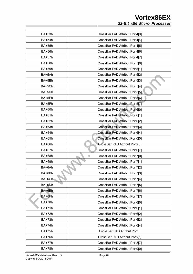
Vortex86EX32-Bit x86 Micro Processor
Vortex86EX datasheet Rev. 1.3 Page 69Copyright © 2013 DMP
BA+53h CrossBar PAD Attribut Port4[3]
BA+54h CrossBar PAD Attribut Port4[4]
BA+55h CrossBar PAD Attribut Port4[5]
BA+56h CrossBar PAD Attribut Port4[6]
BA+57h CrossBar PAD Attribut Port4[7]
BA+58h CrossBar PAD Attribut Port5[0]
BA+59h CrossBar PAD Attribut Port5[1]
BA+5Ah CrossBar PAD Attribut Port5[2]
BA+5Bh CrossBar PAD Attribut Port5[3]
BA+5Ch CrossBar PAD Attribut Port5[4]
BA+5Dh CrossBar PAD Attribut Port5[5]
BA+5Eh CrossBar PAD Attribut Port5[6]
BA+5Fh CrossBar PAD Attribut Port5[7]
BA+60h CrossBar PAD Attribut Port6[0]
BA+61h CrossBar PAD Attribut Port6[1]
BA+62h CrossBar PAD Attribut Port6[2]
BA+63h CrossBar PAD Attribut Port6[3]
BA+64h CrossBar PAD Attribut Port6[4]
BA+65h CrossBar PAD Attribut Port6[5]
BA+66h CrossBar PAD Attribut Por6[6]
BA+67h CrossBar PAD Attribut Port6[7]
BA+68h CrossBar PAD Attribut Port7[0]
BA+69h CrossBar PAD Attribut Port7[1]
BA+6Ah CrossBar PAD Attribut Port7[2]
BA+6Bh CrossBar PAD Attribut Port7[3]
BA+6Ch CrossBar PAD Attribut Port7[4]
BA+6Dh CrossBar PAD Attribut Port7[5]
BA+6Eh CrossBar PAD Attribut Port7[6]
BA+6Fh CrossBar PAD Attribut Port7[7]
BA+70h CrossBar PAD Attribut Port6[0]
BA+71h CrossBar PAD Attribut Port6[1]
BA+72h CrossBar PAD Attribut Port6[2]
BA+73h CrossBar PAD Attribut Port6[3]
BA+74h CrossBar PAD Attribut Port6[4]
BA+75h CrossBar PAD Attribut Port5]
BA+76h CrossBar PAD Attribut Por8[6]
BA+77h CrossBar PAD Attribut Port8[7]
BA+78h CrossBar PAD Attribut Port9[0]
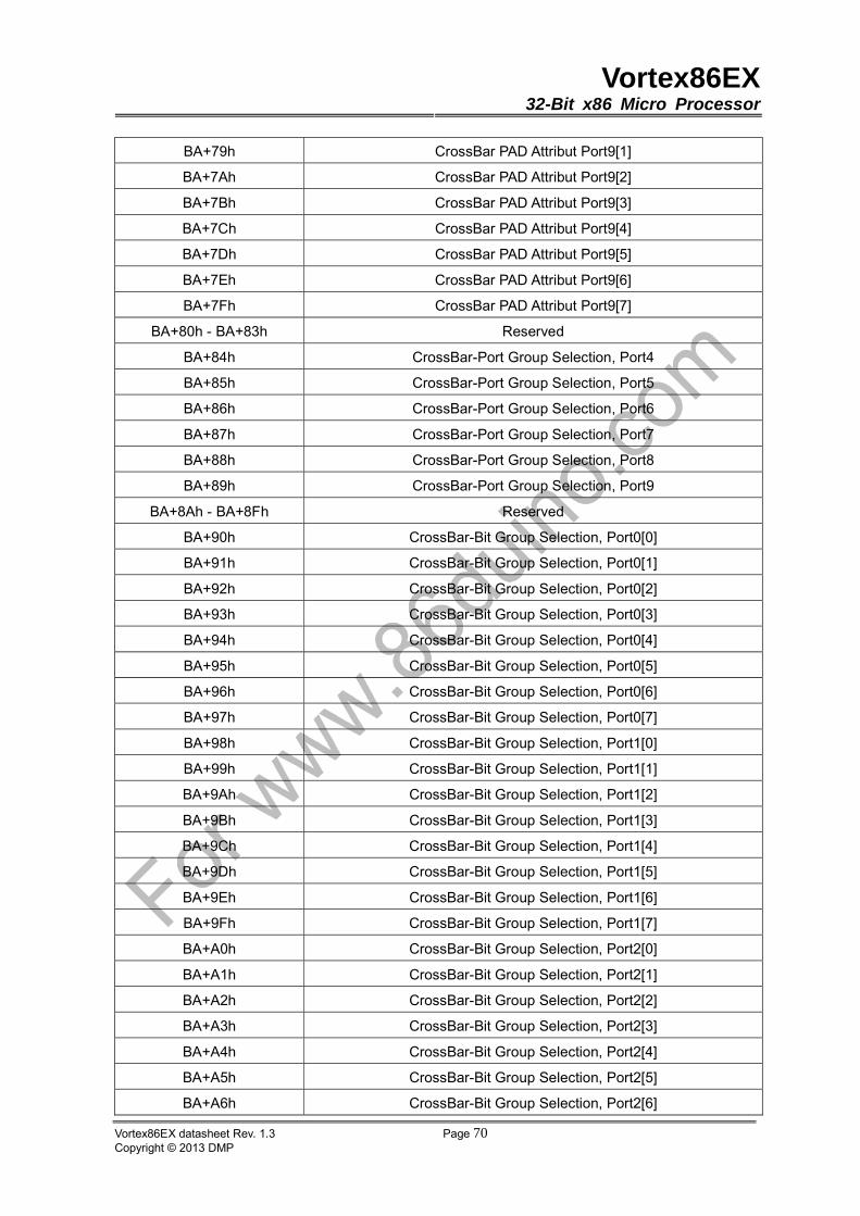
Vortex86EX32-Bit x86 Micro Processor
Vortex86EX datasheet Rev. 1.3 Page 70Copyright © 2013 DMP
BA+79h CrossBar PAD Attribut Port9[1]
BA+7Ah CrossBar PAD Attribut Port9[2]
BA+7Bh CrossBar PAD Attribut Port9[3]
BA+7Ch CrossBar PAD Attribut Port9[4]
BA+7Dh CrossBar PAD Attribut Port9[5]
BA+7Eh CrossBar PAD Attribut Port9[6]
BA+7Fh CrossBar PAD Attribut Port9[7]
BA+80h - BA+83h Reserved
BA+84h CrossBar-Port Group Selection, Port4
BA+85h CrossBar-Port Group Selection, Port5
BA+86h CrossBar-Port Group Selection, Port6
BA+87h CrossBar-Port Group Selection, Port7
BA+88h CrossBar-Port Group Selection, Port8
BA+89h CrossBar-Port Group Selection, Port9
BA+8Ah - BA+8Fh Reserved
BA+90h CrossBar-Bit Group Selection, Port0[0]
BA+91h CrossBar-Bit Group Selection, Port0[1]
BA+92h CrossBar-Bit Group Selection, Port0[2]
BA+93h CrossBar-Bit Group Selection, Port0[3]
BA+94h CrossBar-Bit Group Selection, Port0[4]
BA+95h CrossBar-Bit Group Selection, Port0[5]
BA+96h CrossBar-Bit Group Selection, Port0[6]
BA+97h CrossBar-Bit Group Selection, Port0[7]
BA+98h CrossBar-Bit Group Selection, Port1[0]
BA+99h CrossBar-Bit Group Selection, Port1[1]
BA+9Ah CrossBar-Bit Group Selection, Port1[2]
BA+9Bh CrossBar-Bit Group Selection, Port1[3]
BA+9Ch CrossBar-Bit Group Selection, Port1[4]
BA+9Dh CrossBar-Bit Group Selection, Port1[5]
BA+9Eh CrossBar-Bit Group Selection, Port1[6]
BA+9Fh CrossBar-Bit Group Selection, Port1[7]
BA+A0h CrossBar-Bit Group Selection, Port2[0]
BA+A1h CrossBar-Bit Group Selection, Port2[1]
BA+A2h CrossBar-Bit Group Selection, Port2[2]
BA+A3h CrossBar-Bit Group Selection, Port2[3]
BA+A4h CrossBar-Bit Group Selection, Port2[4]
BA+A5h CrossBar-Bit Group Selection, Port2[5]
BA+A6h CrossBar-Bit Group Selection, Port2[6]
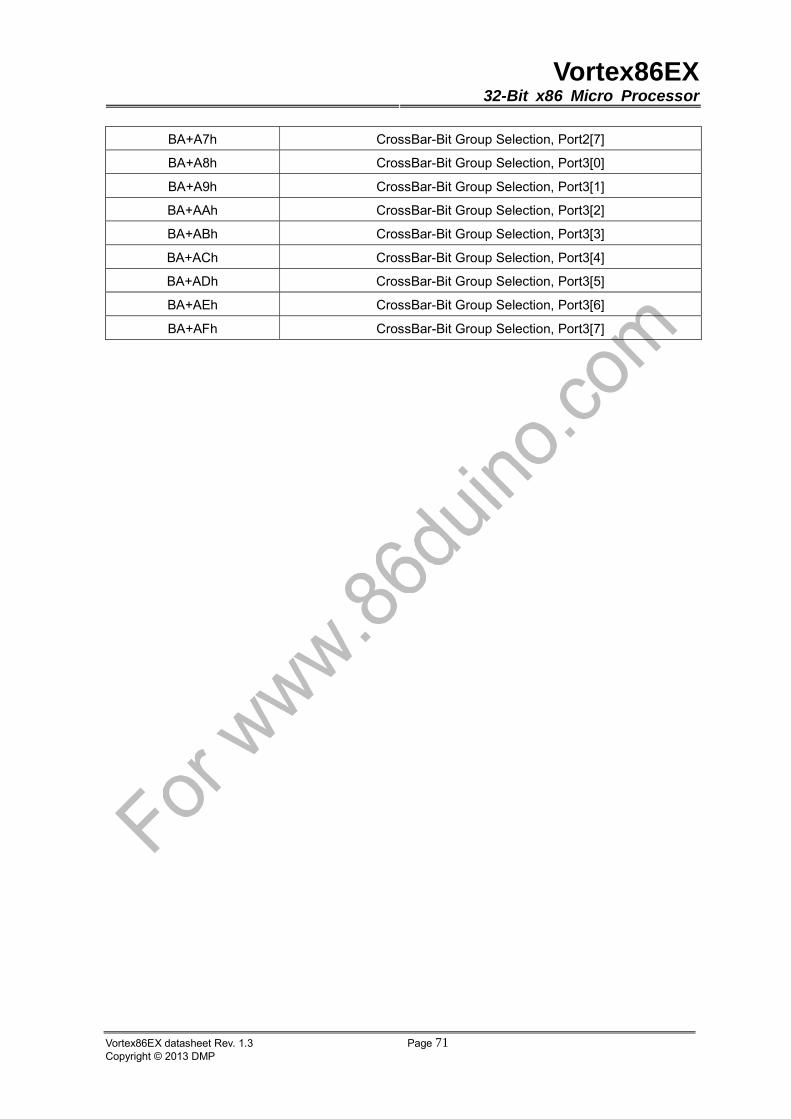
Vortex86EX32-Bit x86 Micro Processor
Vortex86EX datasheet Rev. 1.3 Page 71Copyright © 2013 DMP
BA+A7h CrossBar-Bit Group Selection, Port2[7]
BA+A8h CrossBar-Bit Group Selection, Port3[0]
BA+A9h CrossBar-Bit Group Selection, Port3[1]
BA+AAh CrossBar-Bit Group Selection, Port3[2]
BA+ABh CrossBar-Bit Group Selection, Port3[3]
BA+ACh CrossBar-Bit Group Selection, Port3[4]
BA+ADh CrossBar-Bit Group Selection, Port3[5]
BA+AEh CrossBar-Bit Group Selection, Port3[6]
BA+AFh CrossBar-Bit Group Selection, Port3[7]

Vortex86EX32-Bit x86 Micro Processor
Vortex86EX datasheet Rev. 1.3 Page 72Copyright © 2013 DMP
7.4 Configuration Space Registers
The SoC integrated two PCI base bridges – Host-to-PCI Bridge, ISA-to-PCI Bridge, one MAC, two
IDE, one USB1.1 host, one USB2.0 host and one USB device. These two bridges contain their own
PCI Configuration Space. Configuration Space Registers reside in PCI Configuration Space and
specify PCI configuration, DRAM configuration, operating parameters, and optional system
features.
During hardware reset, the SoC sets its internal configuration registers to predetermine default
states. The default state represents the minimum functionality feature set required to successfully
bring up the system. Hence, it does not represent the optimal system configuration. It is the
responsibility of the system initialization software (usually BIOS) to properly determine the DRAM
configurations, operating parameters and optional system features that are applicable, and to
program the registers accordingly.
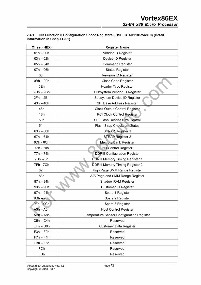
Vortex86EX32-Bit x86 Micro Processor
Vortex86EX datasheet Rev. 1.3 Page 73Copyright © 2013 DMP
7.4.1 NB Function 0 Configuration Space Registers (IDSEL = AD11/Device 0) (Detail information in Chap.11.3.1)
Offset (HEX) Register Name
01h – 00h Vendor ID Register
03h – 02h Device ID Register
05h – 04h Command Register
07h – 06h Status Register
08h Revision ID Register
0Bh – 09h Class Code Register
0Eh Header Type Register
2Dh – 2Ch Subsystem Vendor ID Register
2Fh – 2Eh Subsystem Device ID Register
43h – 40h SPI Base Address Register
48h Clock Output Control Register
4Bh PCI Clock Control Register
50h SPI Flash Decode Size Control
51h Flash Strap Checksum Status
63h – 60h STRAP Register 1
67h – 64h STRAP Register 2
6Dh - 6Ch Memory Bank Register
73h - 70h NB Control Register
77h – 74h DDRIII Configuration Register
7Bh -78h DDRIII Memory Timing Register 1
7Fh - 7Ch DDRIII Memory Timing Register 2
82h High Page SMM Range Register
83h A/B Page and SMM Range Register
87h – 84h Shadow RAM Register
93h – 90h Customer ID Register
97h – 94h Spare 1 Register
9Bh – 98h Spare 2 Register
9Fh – 9Ch Spare 3 Register
A3h – A0h Host Control Register
ABh – A8h Temperature Sensor Configuration Register
C5h – C4h Reserved
EFh – D0h Customer Data Register
F3h – F0h Reserved
F7h – F4h Reserved
FBh – F8h Reserved
FCh Reserved
FDh Reserved
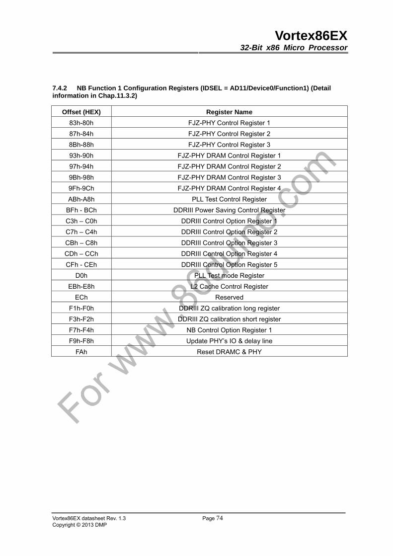
Vortex86EX32-Bit x86 Micro Processor
Vortex86EX datasheet Rev. 1.3 Page 74Copyright © 2013 DMP
7.4.2 NB Function 1 Configuration Registers (IDSEL = AD11/Device0/Function1) (Detail information in Chap.11.3.2)
Offset (HEX) Register Name
83h-80h FJZ-PHY Control Register 1
87h-84h FJZ-PHY Control Register 2
8Bh-88h FJZ-PHY Control Register 3
93h-90h FJZ-PHY DRAM Control Register 1
97h-94h FJZ-PHY DRAM Control Register 2
9Bh-98h FJZ-PHY DRAM Control Register 3
9Fh-9Ch FJZ-PHY DRAM Control Register 4
ABh-A8h PLL Test Control Register
BFh - BCh DDRIII Power Saving Control Register
C3h – C0h DDRIII Control Option Register 1
C7h – C4h DDRIII Control Option Register 2
CBh – C8h DDRIII Control Option Register 3
CDh – CCh DDRIII Control Option Register 4
CFh - CEh DDRIII Control Option Register 5
D0h PLL Test mode Register
EBh-E8h L2 Cache Control Register
ECh Reserved
F1h-F0h DDRIII ZQ calibration long register
F3h-F2h DDRIII ZQ calibration short register
F7h-F4h NB Control Option Register 1
F9h-F8h Update PHY’s IO & delay line
FAh Reset DRAMC & PHY
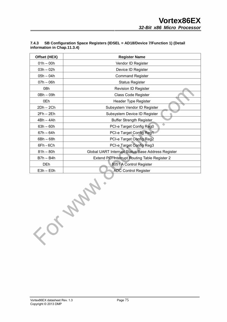
Vortex86EX32-Bit x86 Micro Processor
Vortex86EX datasheet Rev. 1.3 Page 75Copyright © 2013 DMP
7.4.3 SB Configuration Space Registers (IDSEL = AD18/Device 7/Function 1) (Detail information in Chap.11.3.4)
Offset (HEX) Register Name
01h – 00h Vendor ID Register
03h – 02h Device ID Register
05h – 04h Command Register
07h – 06h Status Register
08h Revision ID Register
0Bh – 09h Class Code Register
0Eh Header Type Register
2Dh – 2Ch Subsystem Vendor ID Register
2Fh – 2Eh Subsystem Device ID Register
4Bh – 4Ah Buffer Strength Register
63h – 60h PCI-e Target Config Reg0
67h – 64h PCI-e Target Config Reg1
6Bh – 68h PCI-e Target Config Reg2
6Fh - 6Ch PCI-e Target Config Reg3
81h – 80h Global UART Interrupt Status Base Address Register
B7h – B4h Extend PCI Interrupt Routing Table Register 2
DEh 8051 A Control Register
E3h – E0h ADC Control Register
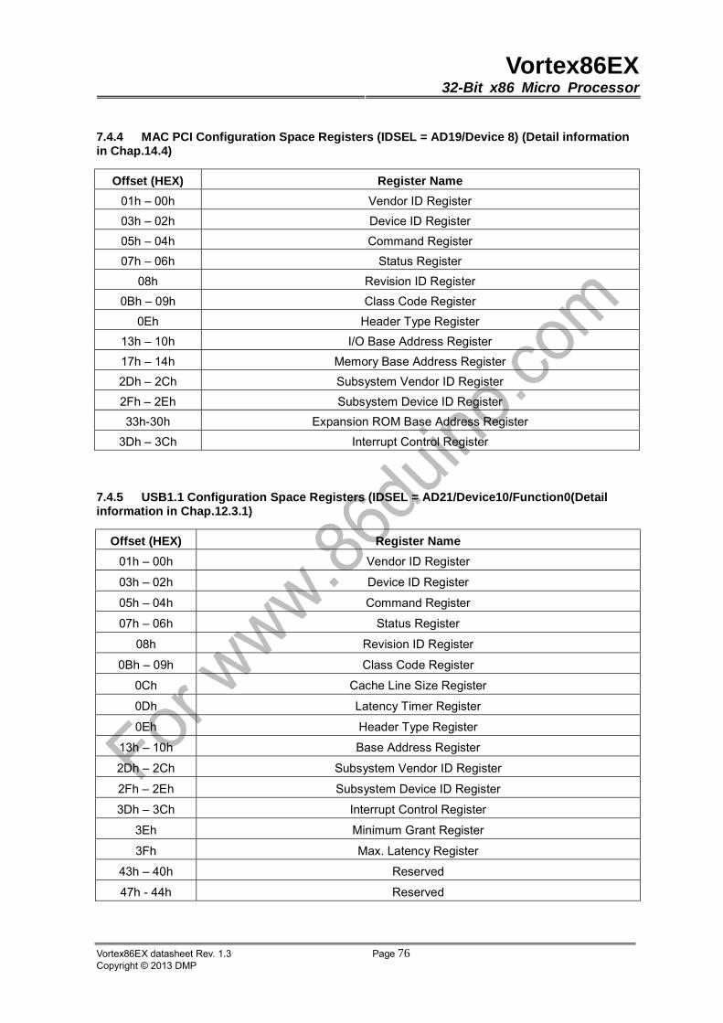
Vortex86EX32-Bit x86 Micro Processor
Vortex86EX datasheet Rev. 1.3 Page 76Copyright © 2013 DMP
7.4.4 MAC PCI Configuration Space Registers (IDSEL = AD19/Device 8) (Detail information in Chap.14.4)
7.4.5 USB1.1 Configuration Space Registers (IDSEL = AD21/Device10/Function0(Detail information in Chap.12.3.1)
Offset (HEX) Register Name
01h – 00h Vendor ID Register
03h – 02h Device ID Register
05h – 04h Command Register
07h – 06h Status Register
08h Revision ID Register
0Bh – 09h Class Code Register
0Eh Header Type Register
13h – 10h I/O Base Address Register
17h – 14h Memory Base Address Register
2Dh – 2Ch Subsystem Vendor ID Register
2Fh – 2Eh Subsystem Device ID Register
33h-30h Expansion ROM Base Address Register
3Dh – 3Ch Interrupt Control Register
Offset (HEX) Register Name
01h – 00h Vendor ID Register
03h – 02h Device ID Register
05h – 04h Command Register
07h – 06h Status Register
08h Revision ID Register
0Bh – 09h Class Code Register
0Ch Cache Line Size Register
0Dh Latency Timer Register
0Eh Header Type Register
13h – 10h Base Address Register
2Dh – 2Ch Subsystem Vendor ID Register
2Fh – 2Eh Subsystem Device ID Register
3Dh – 3Ch Interrupt Control Register
3Eh Minimum Grant Register
3Fh Max. Latency Register
43h – 40h Reserved
47h - 44h Reserved
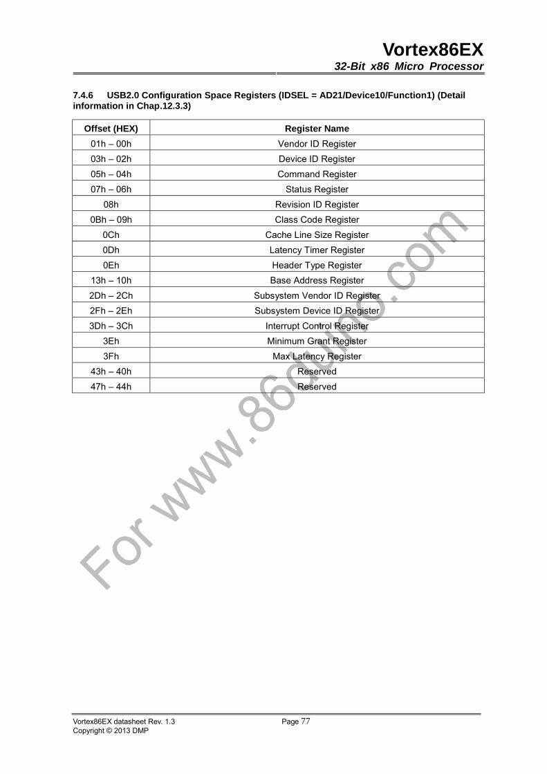
Vortex86EX32-Bit x86 Micro Processor
Vortex86EX datasheet Rev. 1.3 Page 77Copyright © 2013 DMP
7.4.6 USB2.0 Configuration Space Registers (IDSEL = AD21/Device10/Function1) (Detail information in Chap.12.3.3)
Offset (HEX) Register Name
01h – 00h Vendor ID Register
03h – 02h Device ID Register
05h – 04h Command Register
07h – 06h Status Register
08h Revision ID Register
0Bh – 09h Class Code Register
0Ch Cache Line Size Register
0Dh Latency Timer Register
0Eh Header Type Register
13h – 10h Base Address Register
2Dh – 2Ch Subsystem Vendor ID Register
2Fh – 2Eh Subsystem Device ID Register
3Dh – 3Ch Interrupt Control Register
3Eh Minimum Grant Register
3Fh Max Latency Register
43h – 40h Reserved
47h – 44h Reserved
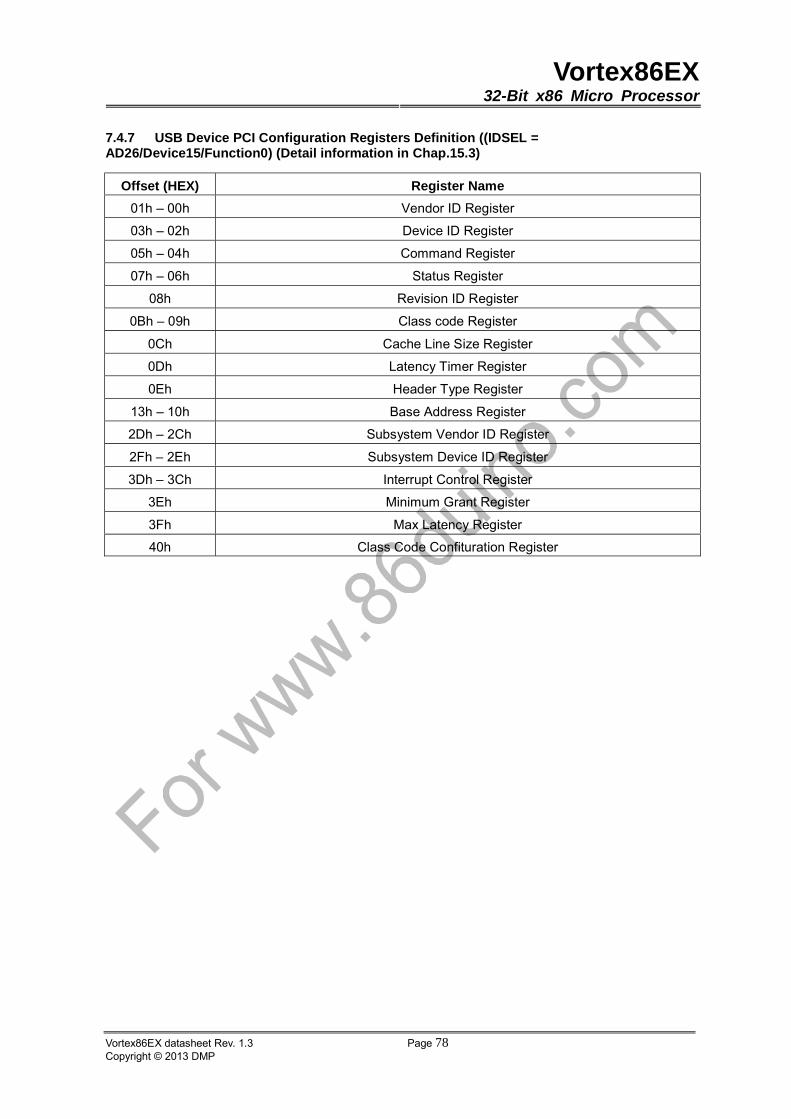
Vortex86EX32-Bit x86 Micro Processor
Vortex86EX datasheet Rev. 1.3 Page 78Copyright © 2013 DMP
7.4.7 USB Device PCI Configuration Registers Definition ((IDSEL = AD26/Device15/Function0) (Detail information in Chap.15.3)
Offset (HEX) Register Name
01h – 00h Vendor ID Register
03h – 02h Device ID Register
05h – 04h Command Register
07h – 06h Status Register
08h Revision ID Register
0Bh – 09h Class code Register
0Ch Cache Line Size Register
0Dh Latency Timer Register
0Eh Header Type Register
13h – 10h Base Address Register
2Dh – 2Ch Subsystem Vendor ID Register
2Fh – 2Eh Subsystem Device ID Register
3Dh – 3Ch Interrupt Control Register
3Eh Minimum Grant Register
3Fh Max Latency Register
40h Class Code Confituration Register
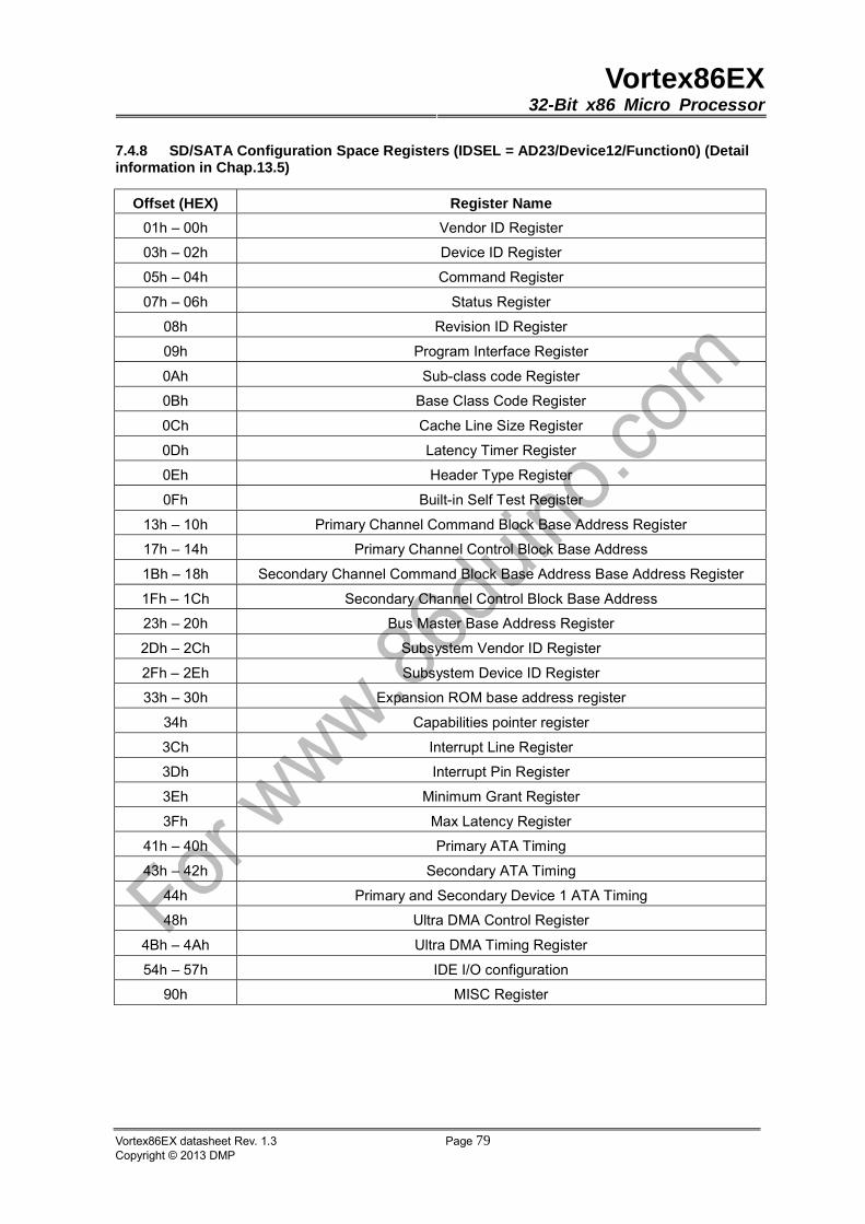
Vortex86EX32-Bit x86 Micro Processor
Vortex86EX datasheet Rev. 1.3 Page 79Copyright © 2013 DMP
7.4.8 SD/SATA Configuration Space Registers (IDSEL = AD23/Device12/Function0) (Detail information in Chap.13.5)
Offset (HEX) Register Name
01h – 00h Vendor ID Register
03h – 02h Device ID Register
05h – 04h Command Register
07h – 06h Status Register
08h Revision ID Register
09h Program Interface Register
0Ah Sub-class code Register
0Bh Base Class Code Register
0Ch Cache Line Size Register
0Dh Latency Timer Register
0Eh Header Type Register
0Fh Built-in Self Test Register
13h – 10h Primary Channel Command Block Base Address Register
17h – 14h Primary Channel Control Block Base Address
1Bh – 18h Secondary Channel Command Block Base Address Base Address Register
1Fh – 1Ch Secondary Channel Control Block Base Address
23h – 20h Bus Master Base Address Register
2Dh – 2Ch Subsystem Vendor ID Register
2Fh – 2Eh Subsystem Device ID Register
33h – 30h Expansion ROM base address register
34h Capabilities pointer register
3Ch Interrupt Line Register
3Dh Interrupt Pin Register
3Eh Minimum Grant Register
3Fh Max Latency Register
41h – 40h Primary ATA Timing
43h – 42h Secondary ATA Timing
44h Primary and Secondary Device 1 ATA Timing
48h Ultra DMA Control Register
4Bh – 4Ah Ultra DMA Timing Register
54h – 57h IDE I/O configuration
90h MISC Register
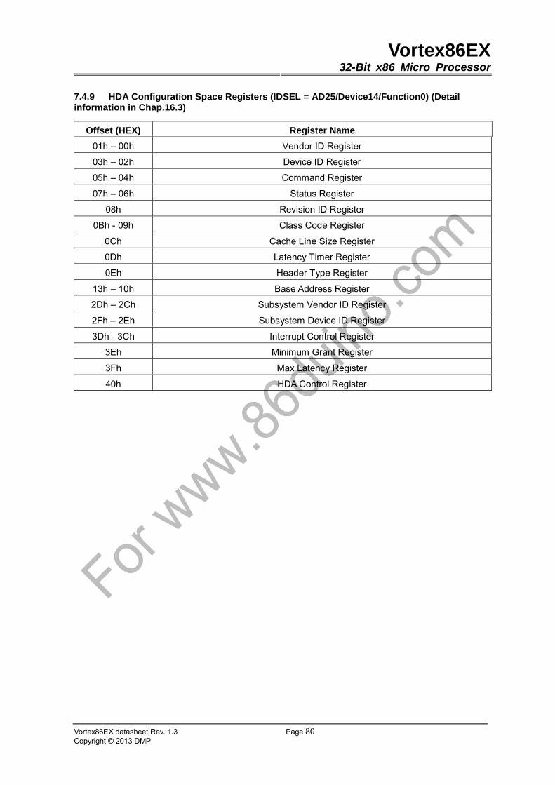
Vortex86EX32-Bit x86 Micro Processor
Vortex86EX datasheet Rev. 1.3 Page 80Copyright © 2013 DMP
7.4.9 HDA Configuration Space Registers (IDSEL = AD25/Device14/Function0) (Detail information in Chap.16.3)
Offset (HEX) Register Name
01h – 00h Vendor ID Register
03h – 02h Device ID Register
05h – 04h Command Register
07h – 06h Status Register
08h Revision ID Register
0Bh - 09h Class Code Register
0Ch Cache Line Size Register
0Dh Latency Timer Register
0Eh Header Type Register
13h – 10h Base Address Register
2Dh – 2Ch Subsystem Vendor ID Register
2Fh – 2Eh Subsystem Device ID Register
3Dh - 3Ch Interrupt Control Register
3Eh Minimum Grant Register
3Fh Max Latency Register
40h HDA Control Register
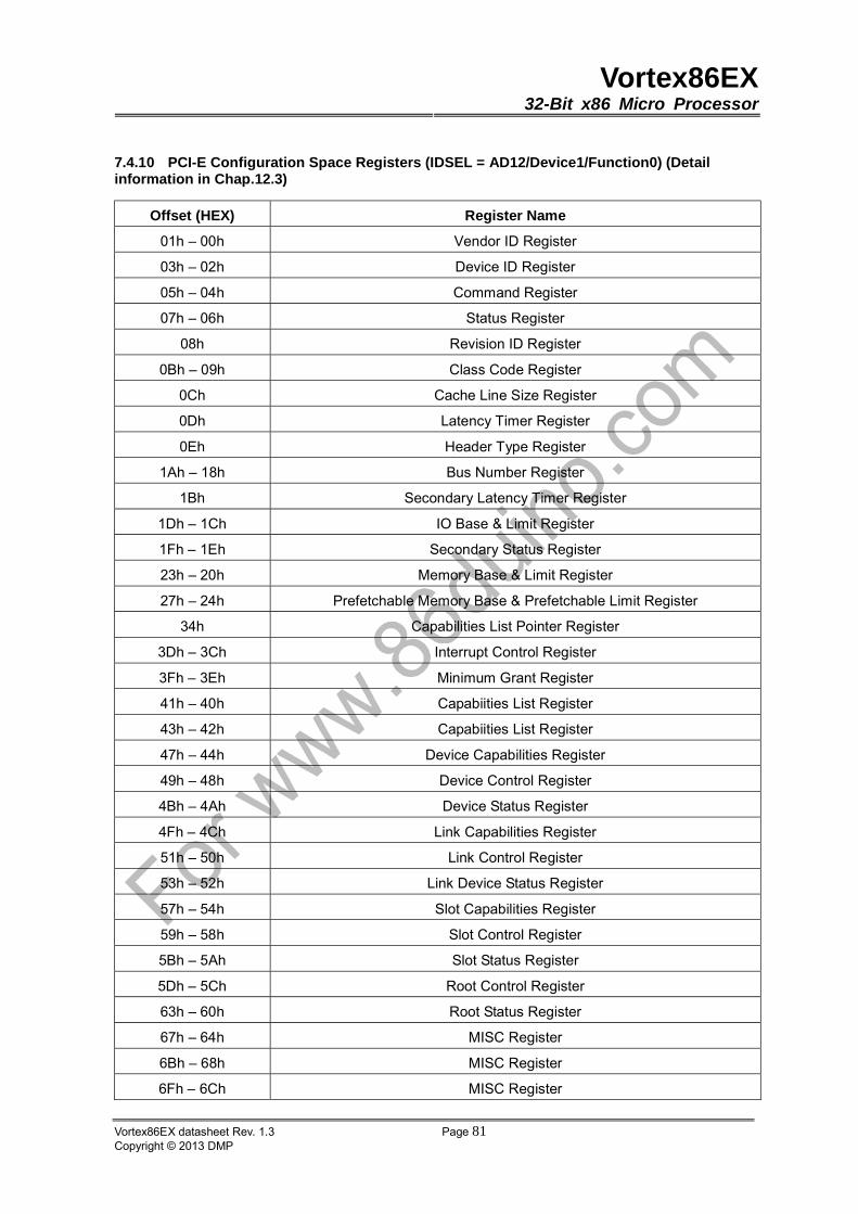
Vortex86EX32-Bit x86 Micro Processor
Vortex86EX datasheet Rev. 1.3 Page 81Copyright © 2013 DMP
7.4.10 PCI-E Configuration Space Registers (IDSEL = AD12/Device1/Function0) (Detail information in Chap.12.3)
Offset (HEX) Register Name
01h – 00h Vendor ID Register
03h – 02h Device ID Register
05h – 04h Command Register
07h – 06h Status Register
08h Revision ID Register
0Bh – 09h Class Code Register
0Ch Cache Line Size Register
0Dh Latency Timer Register
0Eh Header Type Register
1Ah – 18h Bus Number Register
1Bh Secondary Latency Timer Register
1Dh – 1Ch IO Base & Limit Register
1Fh – 1Eh Secondary Status Register
23h – 20h Memory Base & Limit Register
27h – 24h Prefetchable Memory Base & Prefetchable Limit Register
34h Capabilities List Pointer Register
3Dh – 3Ch Interrupt Control Register
3Fh – 3Eh Minimum Grant Register
41h – 40h Capabiities List Register
43h – 42h Capabiities List Register
47h – 44h Device Capabilities Register
49h – 48h Device Control Register
4Bh – 4Ah Device Status Register
4Fh – 4Ch Link Capabilities Register
51h – 50h Link Control Register
53h – 52h Link Device Status Register
57h – 54h Slot Capabilities Register
59h – 58h Slot Control Register
5Bh – 5Ah Slot Status Register
5Dh – 5Ch Root Control Register
63h – 60h Root Status Register
67h – 64h MISC Register
6Bh – 68h MISC Register
6Fh – 6Ch MISC Register
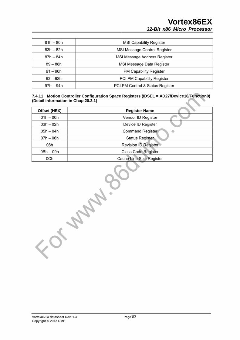
Vortex86EX32-Bit x86 Micro Processor
Vortex86EX datasheet Rev. 1.3 Page 82Copyright © 2013 DMP
81h – 80h MSI Capability Register
83h – 82h MSI Message Control Register
87h – 84h MSI Message Address Register
89 – 88h MSI Message Data Register
91 – 90h PM Capability Register
93 – 92h PCI PM Capability Register
97h – 94h PCI PM Control & Status Register
7.4.11 Motion Controller Configuration Space Registers (IDSEL = AD27/Device16/Function0) (Detail information in Chap.20.3.1)
Offset (HEX) Register Name
01h – 00h Vendor ID Register
03h – 02h Device ID Register
05h – 04h Command Register
07h – 06h Status Register
08h Revision ID Register
0Bh – 09h Class Code Register
0Ch Cache Line Size Register
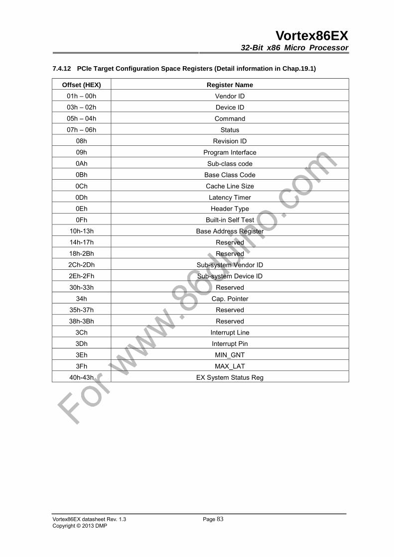
Vortex86EX32-Bit x86 Micro Processor
Vortex86EX datasheet Rev. 1.3 Page 83Copyright © 2013 DMP
7.4.12 PCIe Target Configuration Space Registers (Detail information in Chap.19.1)
Offset (HEX) Register Name
01h – 00h Vendor ID
03h – 02h Device ID
05h – 04h Command
07h – 06h Status
08h Revision ID
09h Program Interface
0Ah Sub-class code
0Bh Base Class Code
0Ch Cache Line Size
0Dh Latency Timer
0Eh Header Type
0Fh Built-in Self Test
10h-13h Base Address Register
14h-17h Reserved
18h-2Bh Reserved
2Ch-2Dh Sub-system Vendor ID
2Eh-2Fh Sub-system Device ID
30h-33h Reserved
34h Cap. Pointer
35h-37h Reserved
38h-3Bh Reserved
3Ch Interrupt Line
3Dh Interrupt Pin
3Eh MIN_GNT
3Fh MAX_LAT
40h-43h EX System Status Reg

Vortex86EX32-Bit x86 Micro Processor
Vortex86EX datasheet Rev. 1.3 Page 84Copyright © 2013 DMP
7.4.13 Duplex SPI Configuration Space Registers (IDSEL = AD27/Device16/Function1) (Detail information in Chap.20.3.2)
Offset (HEX) Register Name
01h – 00h Vendor ID Register
03h – 02h Device ID Register
05h – 04h Command Register
07h – 06h Status Register
08h Revision ID Register
0Bh – 09h Class Code Register
0Ch Cache Line Size Register

Vortex86EX32-Bit x86 Micro Processor
Vortex86EX datasheet Rev. 1.3 Page 85Copyright © 2013 DMP
8. Instruction Set
The SoC core instruction set can be divided into 11 categories of operations:
Data Transfer
Arithmetic
Shift/Rotate
String Manipulation
Bit Manipulation
Control Transfer
High Level Language Support
Operating System Support
Processor Control
All the SoC core instructions operate on 0, 1, 2 or 3 operands, where an operand resides in a
register, in the instruction itself or in memory. Most zero operand instructions (e.g., CLI, STI) take
only one byte. One operand instruction is generally two bytes long. The average instruction is 3.2
bytes long. Since the SoC has a 32-byte instruction queue, an average of 10 instructions will be
prefetched. The use of two operands permits the following types of common instructions:
Register to Register
Memory to Register
Memory to Memory
Immediate to Register
Register to Memory
Immediate to Memory
The operands can be 8-, 16-, or 32-bit long. As a general rule, when 32-bit code is being executed,
operands are 8 or 32 bits; when the existing 80286 or 8086 code (16-bit code) is being executed,
operands are 8 or 16 bits. Prefixes can be added to all instructions, which override the default
length of the operands (i.e., use 32-bit operands for 16-bit code, or 16-bit operands for 32-bit code).
Vortex86EX32-Bit x86 Micro Processor
Vortex86EX datasheet Rev. 1.3 Page 86Copyright © 2013 DMP
9. Addressing Modes
The SoC core provides a total of 11 addressing modes for instructions to specify operands. The
addressing modes are optimized to allow the efficient execution of high-level languages such as C
and FORTRAN, and they cover the vast majority of data references needed by high-level
languages.
9.1 Register and Immediate Modes
Two of the addressing modes provide for instructions that operate on register or immediate
operands:
Register Operand Mode: The operand is located in one of the 8-, 16- or 32-bit general registers.
Immediate Operand Mode: The operand is included in the instruction as part of the opcode.
9.2 32-Bit Memory Addressing Modes
The remaining 9 modes provide a mechanism for specifying the effective address of an operand.
The linear address consists of two components: the segment base address and an effective
address. The effective address is calculated by using combinations of the following four address
elements:
Displacement: An 8-, or 32-bit immediate value, following the instruction.
Base: The contents of any general-purpose register. The base registers are generally used by
compilers to point to the start of the local variable area.
Index: The contents of any general-purpose register except for ESP. The index registers are used
to access the elements of an array, or a string of characters.
Scale: The index register’s value can be multiplied by a scale factor: 1, 2, 4 or 8. Scaled index
mode is especially useful for accessing arrays or structures.
Combinations of these 4 components make up the 9 additional addressing modes. There is no
performance penalty for using any of these addressing combinations, since the effective address
calculation is pipelined with the execution of other instructions. The one exception is the
simultaneous use of Base and Index components, which require one additional clock.
The effective address (EA) of an operand is calculated according to the following formula.
EA = Base Reg + (Index Reg • Scaling) + Displacement
Direct Mode: The operand’s offset is contained as part of the instruction as an 8-, 16- or 32-bit
Vortex86EX32-Bit x86 Micro Processor
Vortex86EX datasheet Rev. 1.3 Page 87Copyright © 2013 DMP
displacement.
Example: INC Word PTR [500]
Register Indirect Mode: A Base register contains the address of the operand.
Example: MOV [ECX], EDX
Based Mode: A Base register’s contents are added to a Displacement to form the operand’s offset.
Example: MOV ECX, [EAX + 24]
Index Mode: An Index register’s contents are added to a Displacement to form the operand’s
offset.
Example: ADD EAX, TABLE[ESI]
Scaled Index Mode: An Index register’s contents are multiplied by a Scaling factor that is added to
a Displacement to form the operand’s offset.
Example: IMUL EBX, TABLE[ESI • 4], 7
Based Index Mode: The contents of a Base register are added to the contents of an Index register
to form the effective address of an operand.
Example: MOV EAX, [ESI] [EBX]
Based Scaled Index Mode: The contents of an Index register is multiplied by a Scaling factor and
the result is added to the contents of a Base register to obtain the operand’s offset.
Example: MOV ECX, [EDX • 8] [EAX]
Based Index Mode with Displacement: The contents of an Index register and a Base register’s
contents and a Displacement are all summed together to form the operand offset.
Example: ADD EDX, [ESI] [EBP + 00FFFFF0H]
Based Scaled Index Mode with Displacement: The contents of an Index register are multiplied by a
Scaling factor and the result is added to the contents of a Base register and a Displacement to
form the operand’s offset.
Example: MOV EAX, LOCALTABLE [EDI • 4] [EBP + 80]

Vortex86EX32-Bit x86 Micro Processor
Vortex86EX datasheet Rev. 1.3 Page 88Copyright © 2013 DMP
9.3 Differences between 16- and 32-bit Addresses
In order to provide software compatibility with the 80286 and 8086, the SoC core can execute 16-bit
instructions in Real and Protected Modes. The processor determines the size of the instructions it is
executing by examining the D bit in the CS segment Descriptor. If the D bit is 0, all operand lengths
and effective addresses are assumed to be 16 bits long. If the D bit is 1, the default length for
operands and addresses is 32 bits. In Real Mode, the default size for operands and addresses is 16
bits.
Regardless of the default precision of the operands or addresses, the SoC core is able to execute
either 16- or 32-bit instructions. This is specified via the use of override prefixes. Two prefixes, the
Operand Size Prefix and the Address Length Prefix, override the value of the D bit on an
individual instruction basis.
Example: The SoC core is executing in Real Mode and the programmer needs to access the EAX
registers. The assembler code for this might be MOV EAX, 32-bit MEMORYOP, and ASM486 Macro
Assembler automatically determines that an Operand Size Prefix is needed and generates it.
Example: The D bit is 0, and the programmer intends to use Scaled Index addressing mode to
access an array. The Address Length Prefix allows the use of MOV DX, TABLE [ESI • 2]. The
assembler uses an Address Length Prefix since, with D= 0, the default addressing mode is 16 bits.
Example: The D bit is 1, and the programmer intends to store a 16-bit quantity. The Operand Length
Prefix is used to specify only a 16-bit value: MOV MEM16, DX.
The OPERAND LENGTH and Address Length Prefixes can be applied separately or in combination
to any instruction. The address Length Prefix does not allow addresses over 64 Kbytes to be
accessed in Real Mode. A memory address that exceeds FFFFH will result in a General Protection
Fault. An Address Length Prefix only allows the use of the additional SoC addressing modes.
When executing 32-bit code, the SoC core uses either 8- or 32-bit displacements, and any register
can be used as base or index registers. When executing 16-bit code, the displacements are either 8
or 16 bits, and the base and index register conform to the 80286 mode 1
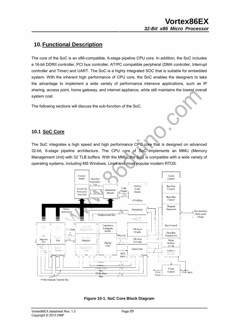
Vortex86EX32-Bit x86 Micro Processor
Vortex86EX datasheet Rev. 1.3 Page 89Copyright © 2013 DMP
10. Functional Description
The core of the SoC is an x86-compatible, 6-stage pipeline CPU core. In addition, the SoC includes
a 16-bit DDRII controller, PCI bus controller, AT/PC compatible peripheral (DMA controller, Interrupt
controller and Timer) and UART. The SoC is a highly integrated SOC that is suitable for embedded
system. With the inherent high performance of CPU core, the SoC enables the designers to take
the advantage to implement a wide variety of performance intensive applications, such as IP
sharing, access point, home gateway, and internet appliance, while still maintains the lowest overall
system cost.
The following sections will discuss the sub-function of the SoC.
10.1 SoC Core
The SoC integrates a high speed and high performance CPU core that is designed on advanced
32-bit, 6-stage pipeline architecture. The CPU core of SoC implements an MMU (Memory
Management Unit) with 32 TLB buffers. With the MMU, the SoC is compatible with a wide variety of
operating systems, including MS Windows, Linux and most popular modern RTOS.
Figure 10-1. SoC Core Block Diagram

Vortex86EX32-Bit x86 Micro Processor
Vortex86EX datasheet Rev. 1.3 Page 90Copyright © 2013 DMP
This SoC core contains all the features of the 486DX microprocessor with enhancements to
increase its performance. The instruction set includes the complete 486SX microprocessor
instruction set along with extensions to serve new applications.
Bus Unit
The bus unit manages data transfers, instruction prefetches and control functions between the
processor’s internal units and the SoC NB. Internally, the bus unit communicates with the cache and
the instruction prefetch units through the 32-bit bus. Externally, the bus unit provides the processor
with bus functions, including external bus cycles, memory read/write, instruction fetch, cache line fill,
etc.,
Prefetch Unit
When the BUS UNIT is not performing bus cycles to execute an instruction, the instruction prefetch
unit uses the BUS UNIT to prefetch instructions. By reading instructions before they are needed, the
processor rarely needs to wait for an instruction prefetch cycle on the processor bus.
Instruction prefetch cycles read 16-byte blocks of instructions, starting at addresses numerically
greater than the last-fetched instruction. The prefetch unit, which has a direct connection to the
paging unit, generates the starting address. The 16-byte prefetched blocks are read into both the
prefetch and cache units simultaneously. The prefetch queue in the prefetch unit stores 32 bytes of
instructions. As each instruction is fetched from the queue, the code part is sent to the instruction
decode unit and (depending on the instruction) the displacement part is sent to the segmentation
unit, where it is used for address calculation. If loops are encountered in the program being
executed, the prefetch unit gets copies of previously executed instructions from the cache.
Decode Unit
The instruction decode unit receives instructions from the instruction prefetch unit and translates
them in a two-stage process into low-level control signals and microcode entry points, as shown in
Figure 10-.1. Most instructions can be decoded at a rate of one per clock.
The decode unit simultaneously processes instruction prefix bytes, opcodes, modR/M bytes, and
displacements. The outputs include hardwired microinstructions to the segmentation, and integer
units. The instruction decode unit is flushed whenever the instruction prefetch unit is flushed.
Memory Management Unit
The on-chip memory management unit (MMU) is completely compatible with the X86
microprocessor.
The memory management unit (MMU) consists of a segmentation unit and a paging unit.
Segmentation allows management of the logical address space by providing easy data and code
relocatability and efficient sharing of global resources. The paging mechanism operates beneath
segmentation and is transparent to the segmentation process. Paging is optional and can be
disabled by system software. Each segment can be divided into one or more 4 Kbytes segments. To

Vortex86EX32-Bit x86 Micro Processor
Vortex86EX datasheet Rev. 1.3 Page 91Copyright © 2013 DMP
implement a virtual memory system, full restartability for all page and segment faults is supported.
Memory is organized into one or more variable length segments, each up to four gigabytes (232
bytes) in size. A segment can have attributes associated with it, which include its location, size, type
(i.e., stack, code or data), and protection characteristics. Each task can have a maximum of 16,381
segments, each up to four gigabytes in size. Thus each task has a maximum of 64 terabytes (trillion
bytes) of virtual memory.
Page TableOffset
Page DirectoryOffset
Page Offset
Page OffsetPage Base Address
Segment OffsetSegment Selector
Logical Address
Linear Address
Physical Address
Translated by the Paging Unit
Translated by the Segmentation Unit
0111231
0111231
03247 31
Figure 10-2. Segmentation and Paging Address Formats
The segmentation unit provides four levels of protection for isolating and protecting applications and
the operating system from each other. The hardware-enforced protection allows the design of
systems with a high degree of integrity.
10.2 L1 Cache
In order to maximize the performance, the SoC integrated a 4-way, 16Kbyte code and 16Kbyte data
cache in it. The level 1 cache supports write through policy. The on-chip L1 cache allows frequently
used data and code to be stored on chip reducing accesses to the external bus. It significantly
reduces the penalty of performance to access these codes and data from external slower memory
devices.

Vortex86EX32-Bit x86 Micro Processor
Vortex86EX datasheet Rev. 1.3 Page 92Copyright © 2013 DMP
10.3 L2 Cache
In order to maximize the performance, the SoC also integrated a 4-way, 128Kbytes cache in it. The
level 2 cache supports write through/write back policy. The on-chip L2 cache allows frequently used
data and code to be stored on chip reducing accesses to the memory. It significantly reduces the
penalty of performance to access these codes and data from external slower memory devices.
10.4 DDR3 Controller
The SoC integrates a main memory DDR3 controller that supports a 16-bit DDR3 data bus width.
The SoC DDR3 interface runs up to 300MHz. All of DDR3 SDRAM configurations provided by SoC
are listed as below:
� DDR3 16-bit data width:
One Chip Select Two Chip Select
DDR3 SDRAM Type DDR3 SDRAM Type Memory
Size X4 X8 X16
Memory
Size X4 X8 X16
64MB 32Mb*16*1*1 64MB
128MB 64Mb*8*2*1 64Mb*16*1*1 128MB 32Mb*16*1*2
256MB 128Mb*4*4*1 128Mb*8*2*1 128Mb*16*1*1 256MB 64Mb*8*2*2 64Mb*16*1*2
512MB 256Mb*4*4*1 256Mb*8*2*1 256Mb*16*1*1 512MB 128Mb*4*4*2 128Mb*8*2*2 128Mb*16*1*2
1GB 512Mb*4*4*1 512Mb*8*2*1 512Mb*16*1*1 1GB 256Mb*4*4*2 256Mb*8*2*2 256Mb*16*1*2
2GB 1Gb*4*4*1 1Gb*8*2*1 2GB 512Mb*4*4*2 512Mb*8*2*2 512Mb*16*1*2
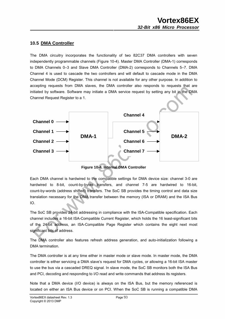
Vortex86EX32-Bit x86 Micro Processor
Vortex86EX datasheet Rev. 1.3 Page 93Copyright © 2013 DMP
10.5 DMA Controller
The DMA circuitry incorporates the functionality of two 82C37 DMA controllers with seven
independently programmable channels (Figure 10-4). Master DMA Controller (DMA-1) corresponds
to DMA Channels 0–3 and Slave DMA Controller (DMA-2) corresponds to Channels 5–7. DMA
Channel 4 is used to cascade the two controllers and will default to cascade mode in the DMA
Channel Mode (DCM) Register. This channel is not available for any other purpose. In addition to
accepting requests from DMA slaves, the DMA controller also responds to requests that are
initiated by software. Software may initiate a DMA service request by setting any bit in the DMA
Channel Request Register to a 1.
Figure 10-4. Internal DMA Controller
Each DMA channel is hardwired to the compatible settings for DMA device size: channel 3-0 are
hardwired to 8-bit, count-by-bytes transfers, and channel 7-5 are hardwired to 16-bit,
count-by-words (address shifted) transfers. The SoC SB provides the timing control and data size
translation necessary for the DMA transfer between the memory (ISA or DRAM) and the ISA Bus
IO.
The SoC SB provides 24-bit addressing in compliance with the ISA-Compatible specification. Each
channel includes a 16-bit ISA-Compatible Current Register, which holds the 16 least-significant bits
of the 24-bit address, an ISA-Compatible Page Register which contains the eight next most
significant bits of address.
The DMA controller also features refresh address generation, and auto-initialization following a
DMA termination.
The DMA controller is at any time either in master mode or slave mode. In master mode, the DMA
controller is either servicing a DMA slave’s request for DMA cycles, or allowing a 16-bit ISA master
to use the bus via a cascaded DREQ signal. In slave mode, the SoC SB monitors both the ISA Bus
and PCI, decoding and responding to I/O read and write commands that address its registers.
Note that a DMA device (I/O device) is always on the ISA Bus, but the memory referenced is
located on either an ISA Bus device or on PCI. When the SoC SB is running a compatible DMA
DMA-1
Channel 0
Channel 1
Channel 2
Channel 3
DMA-2
Channel 4
Channel 5
Channel 6
Channel 7
Vortex86EX32-Bit x86 Micro Processor
Vortex86EX datasheet Rev. 1.3 Page 94Copyright © 2013 DMP
cycle, it drives the MEMR# or MEMW# strobes if the address is less than 16 Mbytes
(000000h–FFFFFFh). These memory strobes are generated regardless of whether the cycle is
decoded for PCI or ISA memory. The SMEMR# and SMEMW# are generated if the address is less
than 1 Mbytes (0000000h–00FFFFFh). If the address is greater than 16 Mbytes
(1000000h–7FFFFFFh), the MEMR# or MEMW# strobe is not generated to avoid aliasing issues.
10.5.1 DMA Transfer Modes
The channels can be programmed for any of four transfer modes. The transfer modes include single,
block, demand, or cascade. Each of the three active transfer modes (single, block, and demand)
can perform three different types of transfers (read, write or verify). Please note that SoC SB does
not support memory-to-memory transfers.
Single Transfer Mode
In single transfer mode, the DMA is programmed to make one transfer only. The byte/word count is
decremented and the address decremented or incremented following each transfer. When the
byte/word count “rolls over” from zero to FFFFh, a Terminal Count (TC) causes an auto-initialization
if the channel has been programmed to do so.
To be recognized, DREQ must be held active until DACK# becomes active. If DREQ is held active
throughout the single transfer, the bus is released after a single transfer. With DREQ asserted high,
the DMA I/O device rearbitrates for the bus. Upon winning the bus, another single transfer is
performed. This allows other ISA bus masters a chance to acquire the bus.
Block Transfer Mode
In Block Transfer mode, the DMA is activated by DREQ to continue making transfers during the
service until a TC, caused by either a byte/word count going to FFFFh, is encountered. DREQ need
only be held active until DACK# becomes active. If the channel has been programmed for it, an
auto-initialization occurs at the end of the service. In this mode, it is possible to lock out other
devices for a period of time (including refresh) if the transfer count is programmed to a large
number.
Demand Transfer Mode
In Demand Transfer mode, the DMA channel is programmed to continue making transfers until a
TC (Terminal Count) is encountered, or until the DMA I/O device releases DREQ. Thus, transfers
may continue until the I/O device has exhausted its data capacity. After the I/O device catches up,
the DMA service is re-established when the DMA I/O device reasserts the channel’s DREQ. During
the time between services when the system is allowed to operate, the intermediate values of
address and byte/word count are stored in the DMA controller Current Address and Current
Byte/Word Count Registers. A TC can cause an auto-initialize at the end of the service, if the
channel has been programmed for it.
Cascade Mode
Vortex86EX32-Bit x86 Micro Processor
Vortex86EX datasheet Rev. 1.3 Page 95Copyright © 2013 DMP
In Cascade Mode, the DMA controller will respond to DREQ with DACK, but SoC SB will not drive
IOR#, IOW#, MEMR#, MEMW#, LA[23:17], SA[19:0], and SBHE#.
Cascade mode is also used to allow direct access of the system by 16-bit bus masters. These
devices use the DREQ and DACK signals to arbitrate for the ISA Bus. The ISA master asserts its
ISA master request line (DREQ[x]) to the DMA internal arbiter. If the ISA master wins the arbitration,
SoC SB responds with an ISA master acknowledge (DACK[x]) signal active. Upon sampling the
DACK[x] line active, the ISA master takes control of the ISA Bus. While an ISA Master owns the bus,
BALE is always driven high while AEN is always driven low. The ISA master has control of the ISA
Bus and may run cycles until it negates the DREQ[x] line.
10.5.2 DMA Transfer Types
Each of the three active transfer modes (Single, Block, or Demand) can perform three different
types of transfers. They are Read, Write and Verify.
Write Transfers
Write transfers move data from an ISA I/O device to memory located on the ISA Bus or in system
DRAM. For transfers using compatible timing, SoC SB will activate ISA Memory control signals to
indicate a memory write as soon as the DMA provides the address. The PCI transfer is initiated
after the data is valid on the ISA Bus. Data steering is used to steer the data to the correct byte lane
during these DMA transfers. When the memory is located on the ISA Bus, a PCI cycle is not
initiated.
The DMA device (I/O device) is either an 8- or 16-bit device and is located on the ISA Bus. The size
of the DMA device is fixed for each channel.
Read Transfers
Read transfers move data from ISA memory or the system DRAM, to an ISA I/O device. SoC SB
activates the IOW# command and the appropriate DRAM and ISA Memory control signals to
indicate a memory read. Data steering is used to steer the data to the correct byte lane during these
DMA transfers. When the cycle involves DRAM, the PCI read transaction is initiated as soon as the
DMA address is valid. When the memory is located on the ISA Bus, a PCI cycle is not initiated.
Verify Transfer
Verify transfers are pseudo transfers. The DMA controller generates addresses as in normal read or
write transfers. However, SoC SB does not activate the ISA memory and I/O control lines. Only the
DACK lines will go active. SoC SB asserts the appropriate DACK signal for nine SYSCLKs. If Verify
transfers are repeated during Block or Demand DMA requests, each additional pseudo transfer will
add eight SYSCLKs. The DACK lines will not be toggled for repeated transfers.
Vortex86EX32-Bit x86 Micro Processor
Vortex86EX datasheet Rev. 1.3 Page 96Copyright © 2013 DMP
10.5.3 DMA Timings
ISA-Compatible timing is provided for ISA DMA slave devices that reside on add in cards. The
repetition rate for ISA-Compatible DMA cycles is eight SYSCLK periods.
When SoC SB negates PHOLD# one clock after driving FRAME# asserted for a bus master IDE
transaction, and another transaction is pending which will cause SoC SB to acquire the PCI bus, it
will drive PHOLD# asserted for the next transaction three clocks after TRDY# is driven negated for
the current transaction.
10.5.4 DREQ and DACK# Latency Control
The SoC SB DMA arbiter maintains a minimum DREQ to DACK# latency on all DMA channels
when programmed in compatible mode. This is to support older devices such as the 8272A. The
DREQs are delayed by eight SYSCLKs prior to being seen by the arbiter logic. This delay
guarantees a minimum 1 msec DREQ to DACK# latency. Software requests will not have this
minimum request to DACK# latency.
10.5.5 Channel Priority
For priority resolution, the DMA consists of two logical channel groups: channel 0–3 and channel
4–7. Each group may be in either fixed or rotate mode, as determined by the DMA Command
Register.
DMA I/O slaves normally assert their DREQ line to arbitrate for DMA service. However, a software
request for DMA service can be presented through each channel’s DMA Request Register. A
software request is subject to the same prioritization as any hardware request. Please see the
detailed register description for Request Register programming information in the DMA Register
description section.
Fixed Priority
The initial fixed priority structure is as follows:
The fixed priority ordering is 0, 1, 2, 3, 5, 6, and 7. In this
scheme, Channel 0 has the highest priority, and channel 7
has the lowest priority. Channel 3-0 of DMA-1 assume the
priority position of Channel 4 in DMA-2, thus take the priority
over channel 5, 6, and 7.
Rotating Priority
Rotation allows for “fairness” in priority resolution. The priority chain rotates so that the last channel
serviced is assigned the lowest priority in the channel group (0–3, 5–7).
Channel 0–3 rotate as a group of four. They are always placed between Channel 5 and Channel 7
High priority...Low priority
(0, 1, 2, 3) (5, 6, 7)

Vortex86EX32-Bit x86 Micro Processor
Vortex86EX datasheet Rev. 1.3 Page 97Copyright © 2013 DMP
in the priority list.
Channel 5–7 rotate as part of a group of four. That is, channel 5–7 form the first three positions in
the rotation, while channel group (0–3) comprises the fourth position in the arbitration.
10.5.6 Register Functionality
Please see the “DMA Register description” section for detailed information on register programming,
bit definitions, and default values/functions of the DMA registers after CPURST is valid.
DMA Channel 4 is used to cascade the two DMA controllers together and should not be
programmed for any mode other than cascade. The DMA Channel Mode Register for channel 4 will
default to cascade mode. Special attention should also be taken when programming the Command
and Mask Registers as related to channel 4.
10.5.7 Address Compatibility Mode
Whenever the DMA is operating, the addresses do not increment or decrement through the High
and Low Page Registers. This is compatible with the 82C37 and Page Register implementation
used in the PC-AT. This mode is set after CPURST is valid.
10.5.8 Summary of DMA Transfer Sizes
Table 10.1 lists each of the DMA device transfer sizes. The column labeled “Current Byte/Word
Count Register” indicates that the register contents represent either the number of bytes to be
transferred or the number of 16-bit words to be transferred. The column labeled “Current Address
Increment/Decrement” indicates the number added to or taken from the Current Address register
after each DMA transfer cycle. The DMA Channel Mode Register determines the Current Address
Register will be incremented or decremented.
Table 10.1: DMA Transfer Size
DMA Device Date Size and Word
Count
Current Byte/Word Count
Register
Current Address
Increment/Decrement
8-Bit I/O, Count by Bytes Bytes Bytes
16-Bit I/O, Count by Words (Address
Shifted)Words 1
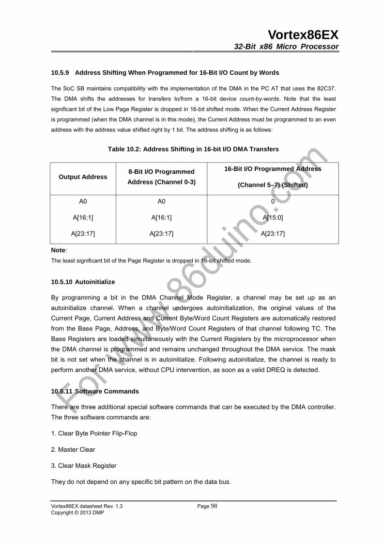
Vortex86EX32-Bit x86 Micro Processor
Vortex86EX datasheet Rev. 1.3 Page 98Copyright © 2013 DMP
10.5.9 Address Shifting When Programmed for 16-Bit I/O Count by Words
The SoC SB maintains compatibility with the implementation of the DMA in the PC AT that uses the 82C37.
The DMA shifts the addresses for transfers to/from a 16-bit device count-by-words. Note that the least
significant bit of the Low Page Register is dropped in 16-bit shifted mode. When the Current Address Register
is programmed (when the DMA channel is in this mode), the Current Address must be programmed to an even
address with the address value shifted right by 1 bit. The address shifting is as follows:
Table 10.2: Address Shifting in 16-bit I/O DMA Transfers
Note:
The least significant bit of the Page Register is dropped in 16-bit shifted mode.
10.5.10 Autoinitialize
By programming a bit in the DMA Channel Mode Register, a channel may be set up as an
autoinitialize channel. When a channel undergoes autoinitialization, the original values of the
Current Page, Current Address and Current Byte/Word Count Registers are automatically restored
from the Base Page, Address, and Byte/Word Count Registers of that channel following TC. The
Base Registers are loaded simultaneously with the Current Registers by the microprocessor when
the DMA channel is programmed and remains unchanged throughout the DMA service. The mask
bit is not set when the channel is in autoinitialize. Following autoinitialize, the channel is ready to
perform another DMA service, without CPU intervention, as soon as a valid DREQ is detected.
10.5.11 Software Commands
There are three additional special software commands that can be executed by the DMA controller.
The three software commands are:
1. Clear Byte Pointer Flip-Flop
2. Master Clear
3. Clear Mask Register
They do not depend on any specific bit pattern on the data bus.
Output Address 8-Bit I/O Programmed
Address (Channel 0-3)
16-Bit I/O Programmed Address
(Channel 5–7) (Shifted)
A0
A[16:1]
A[23:17]
A0
A[16:1]
A[23:17]
0
A[15:0]
A[23:17]
Vortex86EX32-Bit x86 Micro Processor
Vortex86EX datasheet Rev. 1.3 Page 99Copyright © 2013 DMP
Clear Byte Pointer Flip-Flop
This command is executed prior to writing or reading new address or word count information to/from
the DMA controller. This initializes the flip-flop to a known state so that subsequent accesses to
register contents by the microprocessor will address upper and lower bytes in the correct sequence.
When the Host CPU is reading or writing DMA registers, two Byte Pointer flip-flops are used, one
for channel 0–3 and one for channel 4–7. Both of these act independently. There are separate
software commands for clearing each of them (0Ch for channel 0–3, 0D8h for channel 4–7).
DMA Master Clear
This software instruction has the same effect as the hardware reset. The Command, Status,
Request, and Internal First/Last Flip-Flop Registers are cleared and the Mask Register is set. The
DMA controller will enter the idle cycle.
There are two independent master clear commands; 0Dh which acts on channel 0–3, and 0DAh
which acts on channel 4–7.
Clear Mask Register
This command clears the mask bits of all four channels, enabling them to accept DMA requests. I/O
port 00Eh is used for channel 0–3 and I/O port 0DCh for channel 4–7.
Vortex86EX32-Bit x86 Micro Processor
Vortex86EX datasheet Rev. 1.3 Page 100Copyright © 2013 DMP
10.6 Watchdog Timer
The watchdog timer uses 32.768kHz frequency source to count a 24-bit counter so the time range
is from 30.5μ sec to 512 sec with resolution 30.5μ sec. When timer times out, a system reset, NMI
or IRQ may happen to be decided by BIOS programming.
10.6.1 Set the watchdog timer function
Index 37h:
Bit 6=0, Disable watchdog timer
Bit 6=1, Enable watchdog timer
Index 3Ch:
Bit 7=0, Read only/Write one clear, Watchdog timer time out event dose not happen.
Bit 7=1, Read only/Write one clear, Watchdog timer time out event happens.
Index 3Bh, 3Ah, 39h : Counter
10.6.2 Set the watchdog timer Counter
(1) Set Bit 6 = 0 to disable the timer
(2) Write the desired counter value to 3Bh, 3Ah, 39h.
(3) Set Bit 6= 1 to enable the timer, the counter will being to count up.
(4) When counter reaches the setting value, the time out will generate signal setting by index 38h
bit[7:4]
(5) BIOS can read index 3Ch Bit 7 to decide whether the Watchdog timeout event will happen or
not.
3Bh 3Ah 39h
D7……D0 D7……D0 D7……D0
Counter Most SBit……………………………………………………. Least SBit
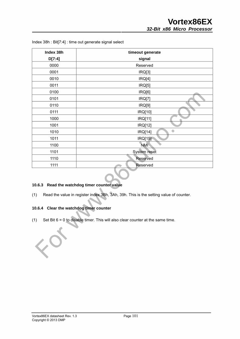
Vortex86EX32-Bit x86 Micro Processor
Vortex86EX datasheet Rev. 1.3 Page 101Copyright © 2013 DMP
Index 38h : Bit[7:4] : time out generate signal select
10.6.3 Read the watchdog timer counter value
(1) Read the value in register index 3Bh, 3Ah, 39h. This is the setting value of counter.
10.6.4 Clear the watchdog timer counter
(1) Set Bit 6 = 0 to disable timer. This will also clear counter at the same time.
Index 38h
D[7:4]
timeout generate
signal
0000 Reserved
0001 IRQ[3]
0010 IRQ[4]
0011 IRQ[5]
0100 IRQ[6]
0101 IRQ[7]
0110 IRQ[9]
0111 IRQ[10]
1000 IRQ[11]
1001 IRQ[12]
1010 IRQ[14]
1011 IRQ[15]
1100 NMI
1101 System reset
1110 Reserved
1111 Reserved
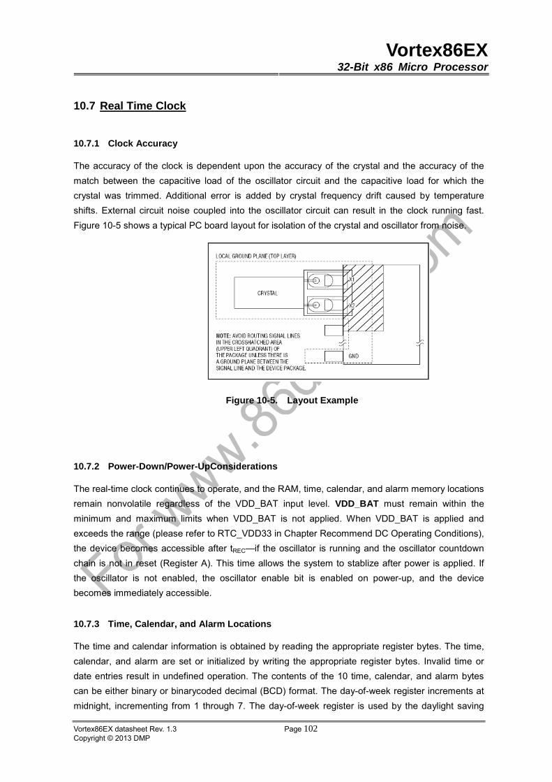
Vortex86EX32-Bit x86 Micro Processor
Vortex86EX datasheet Rev. 1.3 Page 102Copyright © 2013 DMP
10.7 Real Time Clock
10.7.1 Clock Accuracy
The accuracy of the clock is dependent upon the accuracy of the crystal and the accuracy of the
match between the capacitive load of the oscillator circuit and the capacitive load for which the
crystal was trimmed. Additional error is added by crystal frequency drift caused by temperature
shifts. External circuit noise coupled into the oscillator circuit can result in the clock running fast.
Figure 10-5 shows a typical PC board layout for isolation of the crystal and oscillator from noise.
Figure 10-5. Layout Example
10.7.2 Power-Down/Power-UpConsiderations
The real-time clock continues to operate, and the RAM, time, calendar, and alarm memory locations
remain nonvolatile regardless of the VDD_BAT input level. VDD_BAT must remain within the
minimum and maximum limits when VDD_BAT is not applied. When VDD_BAT is applied and
exceeds the range (please refer to RTC_VDD33 in Chapter Recommend DC Operating Conditions),
the device becomes accessible after tREC—if the oscillator is running and the oscillator countdown
chain is not in reset (Register A). This time allows the system to stablize after power is applied. If
the oscillator is not enabled, the oscillator enable bit is enabled on power-up, and the device
becomes immediately accessible.
10.7.3 Time, Calendar, and Alarm Locations
The time and calendar information is obtained by reading the appropriate register bytes. The time,
calendar, and alarm are set or initialized by writing the appropriate register bytes. Invalid time or
date entries result in undefined operation. The contents of the 10 time, calendar, and alarm bytes
can be either binary or binarycoded decimal (BCD) format. The day-of-week register increments at
midnight, incrementing from 1 through 7. The day-of-week register is used by the daylight saving
Vortex86EX32-Bit x86 Micro Processor
Vortex86EX datasheet Rev. 1.3 Page 103Copyright © 2013 DMP
function, so the value 1 is defined as Sunday. The date at the end of the month is automatically
adjusted for months with fewer than 31 days, including correction for leap years. Before writing the
internal time, calendar, and alarm registers, the SET bit in Register B should be written to logic 1 to
prevent updates from occurring while access is being attempted. In addition to writing the 10 time,
calendar, and alarm registers in a selected format (binary or BCD), the data mode bit (DM) of
Register B must be set to the appropriate logic level. All 10 time, calendar, and alarm bytes must
use the same data mode. The SET bit in Register B should be cleared after the data mode bit has
been written to allow the RTC to update the time and calendar bytes. Once initialized, the RTC
makes all updates in the selected mode. The data mode cannot be changed without reinitializing
the 10 data bytes. Tables 2A and 2B show the BCD and binary formats of the time, calendar, and
alarm locations. The 24-12 bit cannot be changed without reinitializing the hour locations. When the
12-hour format is selected, the higher-order bit of the hours byte represents PM when it is logic 1.
The time, calendar, and alarm bytes are always accessible because they are double-buffered. Once
per second the seven bytes are advanced by one second and checked for an alarm condition. If a
read of the time and calendar data occurs during an update, a problem exists where seconds,
minutes, hours, etc., may not correlate. The probability of reading incorrect time and calendar data
is low. Several methods of avoiding any possible incorrect time and calendar reads are covered
later in this text.
The three alarm bytes can be used in two ways. First, when the alarm time is written in the
appropriate hours, minutes, and seconds alarm locations, the alarm interrupt is initiated at the
specified time each day, if the alarm-enable bit is high. In this mode, the “0” bits in the alarm
registers and the corresponding time registers must always be written to 0 (Table 10.3 and 10.4).
Writing the 0 bits in the alarm and/or time registers to 1 can result in undefined operation. The
second use condition is to insert a “don’t care” state in one or more of the three alarm bytes. The
don’t care code is any hexadecimal value from C0 to FF. The two most significant bits of each byte
set the don’t-care condition when at logic 1. An alarm is generated each hour when the don’t-care
bits are set in the hours byte. Similarly, an alarm is generated every minute with don’t-care codes in
the hours and minute alarm bytes. The don’t-care codes in all three alarm bytes create an interrupt
every second.
All 128 bytes can be directly written or read, except for the following:
1) Registers C and D are read-only.
2) Bit 7 of register A is read-only.
3) The MSB of the second byte is read-only.
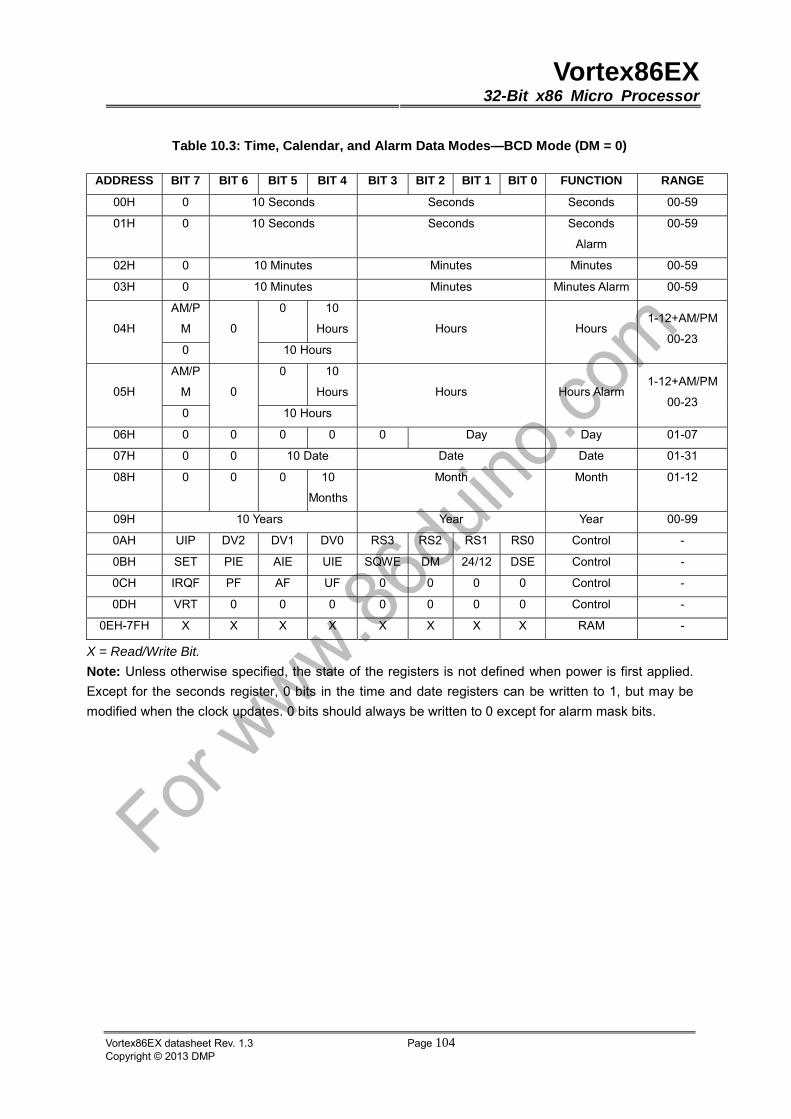
Vortex86EX32-Bit x86 Micro Processor
Vortex86EX datasheet Rev. 1.3 Page 104Copyright © 2013 DMP
Table 10.3: Time, Calendar, and Alarm Data Modes—BCD Mode (DM = 0)
X = Read/Write Bit.
Note: Unless otherwise specified, the state of the registers is not defined when power is first applied.
Except for the seconds register, 0 bits in the time and date registers can be written to 1, but may be
modified when the clock updates. 0 bits should always be written to 0 except for alarm mask bits.
ADDRESS BIT 7 BIT 6 BIT 5 BIT 4 BIT 3 BIT 2 BIT 1 BIT 0 FUNCTION RANGE
00H 0 10 Seconds Seconds Seconds 00-59
01H 0 10 Seconds Seconds Seconds
Alarm
00-59
02H 0 10 Minutes Minutes Minutes 00-59
03H 0 10 Minutes Minutes Minutes Alarm 00-59
AM/P
M
0 10
Hours04H
0
0
10 Hours
Hours Hours 1-12+AM/PM
00-23
AM/P
M
0 10
Hours05H
0
0
10 Hours
Hours Hours Alarm 1-12+AM/PM
00-23
06H 0 0 0 0 0 Day Day 01-07
07H 0 0 10 Date Date Date 01-31
08H 0 0 0 10
Months
Month Month 01-12
09H 10 Years Year Year 00-99
0AH UIP DV2 DV1 DV0 RS3 RS2 RS1 RS0 Control -
0BH SET PIE AIE UIE SQWE DM 24/12 DSE Control -
0CH IRQF PF AF UF 0 0 0 0 Control -
0DH VRT 0 0 0 0 0 0 0 Control -
0EH-7FH X X X X X X X X RAM -

Vortex86EX32-Bit x86 Micro Processor
Vortex86EX datasheet Rev. 1.3 Page 105Copyright © 2013 DMP
Table 10.4 :Time, Calendar, and Alarm Data Modes—Binary Mode (DM =1)
X = Read/Write Bit.
Note: Unless otherwise specified, the state of the registers is not defined when power is first applied.
Except for the seconds register, 0 bits in the time and date registers can be written to 1, but may be
modified when the clock updates. 0 bits should always be written to 0 except for alarm mask bits.
ADDRESS BIT 7 BIT 6 BIT 5 BIT 4 BIT 3 BIT 2 BIT 1 BIT 0 FUNCTION RANGE
00H 0 0 Seconds Seconds 00-3B
01H 0 0 Seconds Seconds
Alarm 00-3B
02H 0 0 Minutes Minutes 00-3B
03H 0 0 Minutes Minutes
Alarm 00-3B
AM/PM 0 Hours 04H
0 0 0
Hours Hours
01-0C+AM/PM
00-17
AM/PM 0 Hours 05H
0 0 0
Hours Hours Alarm
01-0C+AM/PM
00-17
06H 0 0 0 0 0 Day Day 01-07
07H 0 0 0 Date Date 01-1F
08H 0 0 0 0 Month Month 01-0C
09H 0 Year Year 00-63
0AH UIP DV2 DV1 DV0 RS3 RS2 RS1 RS0 Control -
0BH SET PIE AIE UIE SQWE DM 24/12 DSE Control -
0CH IRQF PF AF UF 0 0 0 0 Control -
0DH VRT 0 0 0 0 0 0 0 Control -
0EH-7FH X X X X X X X X RAM -
Vortex86EX32-Bit x86 Micro Processor
Vortex86EX datasheet Rev. 1.3 Page 106Copyright © 2013 DMP
10.7.4 Control Registers
The real-time clocks have four control registers that are accessible at all times, even during the
update cycle.
Control Register A
MSB
LSB
Bit 7: Update-In-Progress (UIP). This bit is a status flag that can be monitored. When the UIP bit is
a 1, the update transfer occurs soon. When UIP is a 0, the update transfer does not occur for at
least 244µs. The time, calendar, and alarm information in RAM is fully available for access when the
UIP bit is 0. The UIP bit is read-only and is not affected by RESET . Writing the SET bit in Register
B to a 1 inhibits any update transfer and clears the UIP status bit.
Bits 6, 5, and 4: DV2, DV1, DV0. These three bits control the clock divider chain and are used to
program the RTC for clock frequencies
The divider chain reset facility can be used for precise timing; when the reset is released, the first
update cycle will occur one half second later. These bits are not affected by NRST.
Bits 3 to 0: Rate Selector (RS3, RS2, RS1, RS0). These four rate-selection bits select one of the
13 taps onthe15-stage divider or disable the divider output. The tap selected can be used to
generate an output square wave (SQW pin) and/or a periodic interrupt. The user can do one of the
following:
1) Enable the interrupt with the PIE bit;
2) Enable the SQW output pin with the SQWE bit;
BIT7 BIT6 BIT5 BIT4 BIT3 BIT2 BIT1 BIT0
UIP DV2 DV1 DV0 RS3 RS2 RS1 RS0
DV2 DV1 DV0 Clock Frequency Comment
0 0 0 X Not support
0 0 1 X
0 1 0 32768Hz
1 X X Any Divider chain held reset
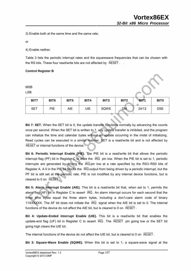
Vortex86EX32-Bit x86 Micro Processor
Vortex86EX datasheet Rev. 1.3 Page 107Copyright © 2013 DMP
3) Enable both at the same time and the same rate;
or
4) Enable neither.
Table 3 lists the periodic interrupt rates and the squarewave frequencies that can be chosen with
the RS bits. These four read/write bits are not affected by RESET . .
Control Register B
MSB
LSB
Bit 7: SET. When the SET bit is 0, the update transfer functions normally by advancing the counts
once per second. When the SET bit is written to 1, any update transfer is inhibited, and the program
can initialize the time and calendar bytes without an update occurring in the midst of initializing.
Read cycles can be executed in a similar manner. SET is a read/write bit and is not affected by
RESET or internal functions of the device.
Bit 6: Periodic Interrupt Enable (PIE). The PIE bit is a read/write bit that allows the periodic
interrupt flag (PF) bit in Register C to drive the IRQ pin low. When the PIE bit is set to 1, periodic
interrupts are generated by driving the IRQ pin low at a rate specified by the RS3–RS0 bits of
Register A. A 0 in the PIE bit blocks the IRQ output from being driven by a periodic interrupt, but the
PF bit is still set at the periodic rate. PIE is not modified by any internal device functions, but is
cleared to 0 on RESET .
Bit 5: Alarm Interrupt Enable (AIE). This bit is a read/write bit that, when set to 1, permits the
alarm flag (AF) bit in Register C to assert IRQ . An alarm interrupt occurs for each second that the
three time bytes equal the three alarm bytes, including a don’t-care alarm code of binary
11XXXXXX. The AF bit does not initiate the IRQ signal when the AIE bit is set to 0. The internal
functions of the device do not affect the AIE bit, but is cleared to 0 on RESET .
Bit 4: Update-Ended Interrupt Enable (UIE). This bit is a read/write bit that enables the
update-end flag (UF) bit in Register C to assert IRQ . The RESET pin going low or the SET bit
going high clears the UIE bit.
The internal functions of the device do not affect the UIE bit, but is cleared to 0 on RESET .
Bit 3: Square-Wave Enable (SQWE). When this bit is set to 1, a square-wave signal at the
BIT7 BIT6 BIT5 BIT4 BIT3 BIT2 BIT1 BIT0
SET PIE AIE UIE SQWE DM 24/12 DSE
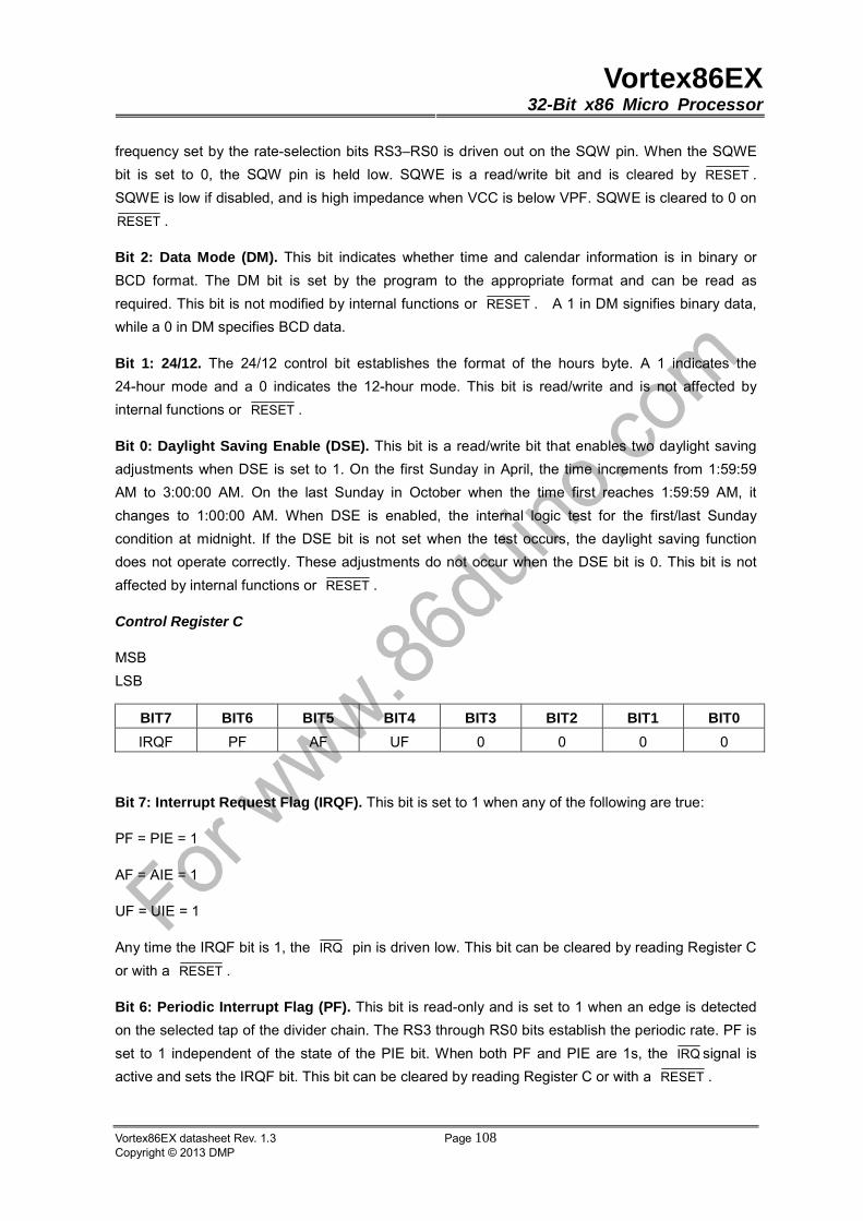
Vortex86EX32-Bit x86 Micro Processor
Vortex86EX datasheet Rev. 1.3 Page 108Copyright © 2013 DMP
frequency set by the rate-selection bits RS3–RS0 is driven out on the SQW pin. When the SQWE
bit is set to 0, the SQW pin is held low. SQWE is a read/write bit and is cleared by RESET .
SQWE is low if disabled, and is high impedance when VCC is below VPF. SQWE is cleared to 0 on
RESET .
Bit 2: Data Mode (DM). This bit indicates whether time and calendar information is in binary or
BCD format. The DM bit is set by the program to the appropriate format and can be read as
required. This bit is not modified by internal functions or RESET . A 1 in DM signifies binary data,
while a 0 in DM specifies BCD data.
Bit 1: 24/12. The 24/12 control bit establishes the format of the hours byte. A 1 indicates the
24-hour mode and a 0 indicates the 12-hour mode. This bit is read/write and is not affected by
internal functions or RESET .
Bit 0: Daylight Saving Enable (DSE). This bit is a read/write bit that enables two daylight saving
adjustments when DSE is set to 1. On the first Sunday in April, the time increments from 1:59:59
AM to 3:00:00 AM. On the last Sunday in October when the time first reaches 1:59:59 AM, it
changes to 1:00:00 AM. When DSE is enabled, the internal logic test for the first/last Sunday
condition at midnight. If the DSE bit is not set when the test occurs, the daylight saving function
does not operate correctly. These adjustments do not occur when the DSE bit is 0. This bit is not
affected by internal functions or RESET .
Control Register C
MSB
LSB
Bit 7: Interrupt Request Flag (IRQF). This bit is set to 1 when any of the following are true:
PF = PIE = 1
AF = AIE = 1
UF = UIE = 1
Any time the IRQF bit is 1, the IRQ pin is driven low. This bit can be cleared by reading Register C
or with a RESET .
Bit 6: Periodic Interrupt Flag (PF). This bit is read-only and is set to 1 when an edge is detected
on the selected tap of the divider chain. The RS3 through RS0 bits establish the periodic rate. PF is
set to 1 independent of the state of the PIE bit. When both PF and PIE are 1s, the IRQ signal is
active and sets the IRQF bit. This bit can be cleared by reading Register C or with a RESET .
BIT7 BIT6 BIT5 BIT4 BIT3 BIT2 BIT1 BIT0
IRQF PF AF UF 0 0 0 0
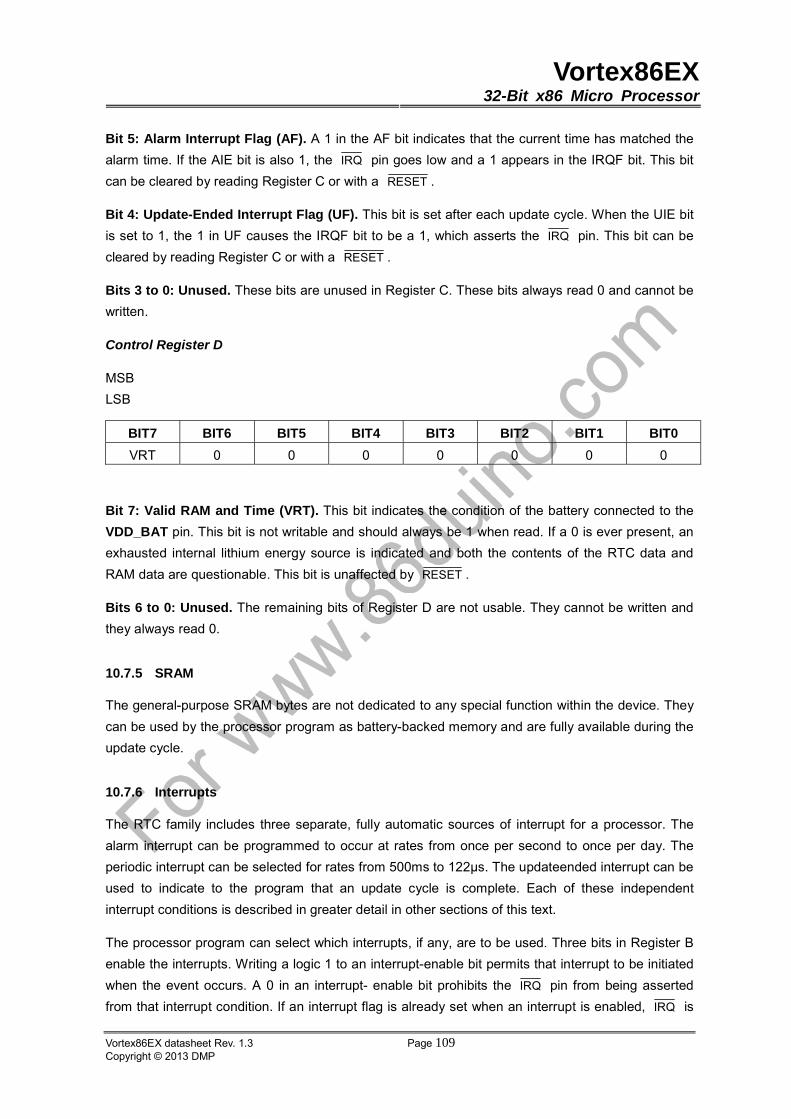
Vortex86EX32-Bit x86 Micro Processor
Vortex86EX datasheet Rev. 1.3 Page 109Copyright © 2013 DMP
Bit 5: Alarm Interrupt Flag (AF). A 1 in the AF bit indicates that the current time has matched the
alarm time. If the AIE bit is also 1, the IRQ pin goes low and a 1 appears in the IRQF bit. This bit
can be cleared by reading Register C or with a RESET .
Bit 4: Update-Ended Interrupt Flag (UF). This bit is set after each update cycle. When the UIE bit
is set to 1, the 1 in UF causes the IRQF bit to be a 1, which asserts the IRQ pin. This bit can be
cleared by reading Register C or with a RESET .
Bits 3 to 0: Unused. These bits are unused in Register C. These bits always read 0 and cannot be
written.
Control Register D
MSB
LSB
Bit 7: Valid RAM and Time (VRT). This bit indicates the condition of the battery connected to the
VDD_BAT pin. This bit is not writable and should always be 1 when read. If a 0 is ever present, an
exhausted internal lithium energy source is indicated and both the contents of the RTC data and
RAM data are questionable. This bit is unaffected by RESET .
Bits 6 to 0: Unused. The remaining bits of Register D are not usable. They cannot be written and
they always read 0.
10.7.5 SRAM
The general-purpose SRAM bytes are not dedicated to any special function within the device. They
can be used by the processor program as battery-backed memory and are fully available during the
update cycle.
10.7.6 Interrupts
The RTC family includes three separate, fully automatic sources of interrupt for a processor. The
alarm interrupt can be programmed to occur at rates from once per second to once per day. The
periodic interrupt can be selected for rates from 500ms to 122µs. The updateended interrupt can be
used to indicate to the program that an update cycle is complete. Each of these independent
interrupt conditions is described in greater detail in other sections of this text.
The processor program can select which interrupts, if any, are to be used. Three bits in Register B
enable the interrupts. Writing a logic 1 to an interrupt-enable bit permits that interrupt to be initiated
when the event occurs. A 0 in an interrupt- enable bit prohibits the IRQ pin from being asserted
from that interrupt condition. If an interrupt flag is already set when an interrupt is enabled, IRQ is
BIT7 BIT6 BIT5 BIT4 BIT3 BIT2 BIT1 BIT0
VRT 0 0 0 0 0 0 0
Vortex86EX32-Bit x86 Micro Processor
Vortex86EX datasheet Rev. 1.3 Page 110Copyright © 2013 DMP
immediately set at an active level, although the interrupt initiating the event may have occurred
earlier. As a result, there are cases where the program should clear such earlier initiated interrupts
before first enabling new interrupts.
When an interrupt event occurs, the relating flag bit is set to logic 1 in Register C. These flag bits
are set independent of the state of the corresponding enable bit in Register B. The flag bit can be
used in a polling mode without enabling the corresponding enable bits. The interrupt flag bit is a
status bit that software can interrogate as necessary. When a flag is set, an indication is given to
software that an interrupt event has occurred since the flag bit was last read; however, care should
be taken when using the flag bits as they are cleared each time Register C is read. Double latching
is included
with Register C so that bits that are set remain stable throughout the read cycle. All bits that are set
(high) are cleared when read, and new interrupts that are pending during the read cycle are held
until after the cycle is completed. One, two, or three bits can be set when reading Register C. Each
used flag bit should be examined when Register C is read to ensure that no interrupts are lost.
The second flag bit method is used with fully enabled interrupts. When an interrupt flag bit is set and
the corresponding interrupt-enable bit is also set, the IRQ pin is asserted low. IRQ is asserted as
long as at least one of the three interrupt sources has its flag and enable bits set. The IRQF bit in
Register C is a 1 whenever the IRQ pin is driven low. Determination that the RTC initiated an
interrupt is accomplished by reading Register C. A logic 1 in bit 7 (IRQF bit) indicates that one or
more interrupts have been initiated by the device. The act of reading Register C clears all active flag
bits and the IRQF bit.
10.7.7 Oscillator Control Bits
When SoC are shipped from the factory, the internal oscillator is turned off. This prevents the lithium
energy cell from being used until the device is installed in a system.
A pattern of 010 in bits 4 to 6 of Register A turns the oscillator on and enables the countdown chain.
A pattern of 1xx (DV2 = 1, DV1 = X, DV0 = X) turns the oscillator on, but holds the countdown chain
of the oscillator in reset. All other combinations of bits 4 to 6 keep the oscillator off.
10.7.8 Periodic Interrupt Selection
The periodic interrupt causes the IRQ pin to go to an active state from once every 500ms to once
every 122µs. This function is separate from the alarm interrupt, which can be output from once per
second to once per day. The periodic interrupt rate is selected using the same Register A bits that
select the square-wave frequency (Table 10.5). Changing the Register A bits affects the
square-wave frequency and the periodic-interrupt output. However, each function has a separate
enable bit in Register B. The SQWE bit controls the square-wave output. Similarly, the PIE bit in
Register B enables the periodic interrupt. The periodic interrupt can be used with software counters
to measure inputs, create output intervals, or await the next needed software function.
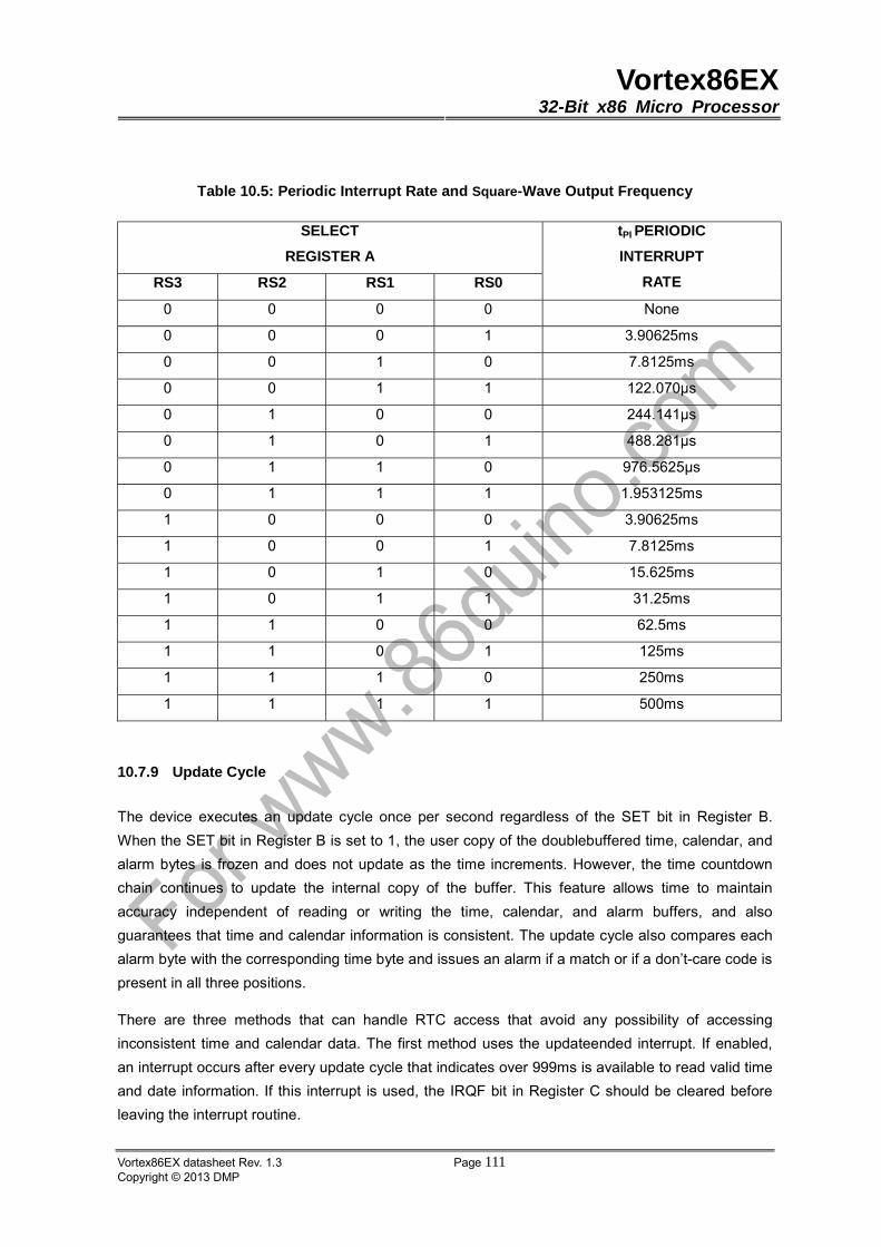
Vortex86EX32-Bit x86 Micro Processor
Vortex86EX datasheet Rev. 1.3 Page 111Copyright © 2013 DMP
Table 10.5: Periodic Interrupt Rate and Square-Wave Output Frequency
10.7.9 Update Cycle
The device executes an update cycle once per second regardless of the SET bit in Register B.
When the SET bit in Register B is set to 1, the user copy of the doublebuffered time, calendar, and
alarm bytes is frozen and does not update as the time increments. However, the time countdown
chain continues to update the internal copy of the buffer. This feature allows time to maintain
accuracy independent of reading or writing the time, calendar, and alarm buffers, and also
guarantees that time and calendar information is consistent. The update cycle also compares each
alarm byte with the corresponding time byte and issues an alarm if a match or if a don’t-care code is
present in all three positions.
There are three methods that can handle RTC access that avoid any possibility of accessing
inconsistent time and calendar data. The first method uses the updateended interrupt. If enabled,
an interrupt occurs after every update cycle that indicates over 999ms is available to read valid time
and date information. If this interrupt is used, the IRQF bit in Register C should be cleared before
leaving the interrupt routine.
SELECT
REGISTER A
RS3 RS2 RS1 RS0
tPI PERIODIC
INTERRUPT
RATE
0 0 0 0 None
0 0 0 1 3.90625ms
0 0 1 0 7.8125ms
0 0 1 1 122.070μs
0 1 0 0 244.141μs
0 1 0 1 488.281μs
0 1 1 0 976.5625μs
0 1 1 1 1.953125ms
1 0 0 0 3.90625ms
1 0 0 1 7.8125ms
1 0 1 0 15.625ms
1 0 1 1 31.25ms
1 1 0 0 62.5ms
1 1 0 1 125ms
1 1 1 0 250ms
1 1 1 1 500ms

Vortex86EX32-Bit x86 Micro Processor
Vortex86EX datasheet Rev. 1.3 Page 112Copyright © 2013 DMP
A second method uses the update-in-progress bit (UIP) in Register A to determine if the update
cycle is in progress. The UIP bit pulses once per second. After the UIP bit goes high, the update
transfer occurs 244µs later. If a low is read on the UIP bit, the user has at least 244µs before the
time/calendar data is changed. Therefore, the user should avoid interrupt service routines that
would cause the time needed to read valid time/calendar data to exceed 244µs.
The third method uses a periodic interrupt to determine if an update cycle is in progress. The UIP bit
in Register A is set high between the setting of the PF bit in Register C (Figure 10-6). Periodic
interrupts that occur at a rate greater than tBUC allow valid time and date information to be reached
at each occurrence of the periodic interrupt. The reads should be complete within 1(tPI/2 + tBUC) to
ensure that data is not read during the update cycle.
Figure 10-6. UIP and Periodic Interrupt Timing
10.8 ProgrammableTimer
SoC SB contains three counters that are equivalent to those found in the 82C54 programmable
interval timer. The three counters are contained in one timer unit, referred to as Timer-1. Each
counter output provides a key system function. Counter 0 is connected to interrupt controller IRQ0
and provides a system timer interrupt for a time-of-day, diskette time-out, or other system timing
functions. Counter 1 generates a refresh request signal and Counter 2 generates the tone for the
speaker. The 14.31818-MHz counters normally use OSC as a clock source.
Counter 0, System Timer
This counter functions as the system timer by controlling the state of IRQ0 and is typically
programmed for Mode 3 operation. The counter produces a square wave with a period equal to the
product of the counter period (838 ns) and the initial count value. The counter loads the initial count
value one counter period after software writes the count value to the counter I/O address. The
counter initially asserts IRQ0 and decrements the count value by two each counter period. The
counter negates IRQ0 when the count value reaches 0. It then reloads the initial count value and

Vortex86EX32-Bit x86 Micro Processor
Vortex86EX datasheet Rev. 1.3 Page 113Copyright © 2013 DMP
again decrements the initial count value by two each counter period. The counter then asserts IRQ0
when the count value reaches 0, reloads the initial count value, and repeats the cycle, alternately
asserting and negating IRQ0.
Counter 1, Refresh Request Signal
This counter provides the refresh request signal and is typically programmed for Mode 2 operation.
The counter negates refresh request for one counter period (838 ns) during each count cycle. The
initial count value is loaded one counter period after being written to the counter I/O address. The
counter initially asserts refresh request, and negates it for one counter period when the count value
reaches 1. The counter then asserts refresh request and continues counting from the initial count
value.
Counter 2, Speaker Tone
This counter provides the speaker tone and is typically programmed for Mode 3 operation. The
counter provides a speaker frequency equal to the counter clock frequency (1.193 MHz) divided by
the initial count value. The speaker must be enabled by a write to port 061h (see NMI Status and
Control ports).
10.8.1 Programming the Interval Timer
The counter/timers are programmed by I/O accesses and are addressed as though they are
contained in one 82C54 interval timer. A single Control Word Register controls the operation of all
three counters. The interval timer is an I/O-mapped device. Several commands are available:
The Control Word Command specifies:
which counter to read or write
the operating mode
the count format (binary or BCD)
The Counter Latch Command latches the current count so that it can be read by the system. The
countdown process continues. The Read Back Command reads the count value, programmed
mode, the current state of the OUT pins, and the state of the Null Count Flag of the selected
counter.
The Read/Write Logic selects the Control Word Register during an I/O write when address lines
A[1:0]=11. This condition occurs during an I/O write to port address 043h, the address for the
Control Word Register on Timer 1. If the CPU writes to port 043h, the data is stored in the Control
Word Register and is interpreted as the Control Word used to define the operation of the Counters.
The Control Word Register is write only. Counter status information is available with the read back
Command.
Vortex86EX32-Bit x86 Micro Processor
Vortex86EX datasheet Rev. 1.3 Page 114Copyright © 2013 DMP
Because the timer counters wake up in an unknown state after power up, multiple refresh requests
may be queued. To avoid possible multiple refresh cycles after power up, program the timer counter
immediately after power up.
Write Operations
Programming the interval timer is a simple process:
1. Write a control word.
2. Write an initial count for each counter.
3. Load the least and/or most significant bytes (as required by Control Word bit 5 and 4) of the
16-bit counter.
The programming procedure for the SoC SB timer is very flexible. Only two conventions need to be
observed. First, for each counter, the control word must be written before the initial count is written.
Second, the initial count must follow the count format specified in the control word (least significant
byte only, most significant byte only, or least significant byte and then most significant byte).
Since the Control Word Register and the three counters have separate addresses (selected by the
A1 and A0 inputs), and each control word specifies the counter it applies to (SC0 and SC1 bits), no
special instruction sequence is required. Any programming sequence that follows the conventions
above is acceptable.
A new initial count may be written to a counter at any time without affecting the counter’s
programmed mode. Counting will be affected as described in the mode definitions. The new count
must follow the programmed count format.
If a counter is programmed to read/write 2-byte counts, the following precaution applies: A program
must not transfer control between writing the first and second byte to another routine which also
writes into that same counter. Otherwise, the counter will be loaded with an incorrect count.
Interval Timer Control Word Format
The control word specifies the counter, the operating mode, the order and size of the count value,
and whether it counts down in a 16-bit or binary-coded decimal (BCD) format. After writing the
control word, a new count may be written at any time. The new value will take effect according to
the programmed mode.
If a counter is programmed to read/write 2-byte counts, the following precaution applies: A program
must not transfer control between writing the first and second byte to another routine which also
writes into that same counter. Otherwise, the counter will be loaded with an incorrect count. The
count must always be completely loaded with both bytes.
Read Operations
It is often desirable to read the value of a counter without disturbing the count in progress. There

Vortex86EX32-Bit x86 Micro Processor
Vortex86EX datasheet Rev. 1.3 Page 115Copyright © 2013 DMP
are three possible methods for reading the counters: a simple read operation, the Counter Latch
Command, and the Read Back Command.
Counter I/O Port Read
The first method is to perform a simple read operation. To read the counter, which is selected with
the A1 and A0 inputs (port 040h, 041h, or 042h), the CLK input of the selected counter must be
inhibited by using either the GATE input or external logic. Otherwise, the count may be in the
process of changing when it is read, giving an undefined result. When reading the count value
directly, follow the format programmed in the control register: read LSB, read MSB, or read LSB
then MSB. Within the SoC SB timer unit, the GATE input on Counter 0 and Counter 1 is tied high.
Therefore, the direct register read should not be used on these two counters. The GATE input of
Counter 2 is controlled through I/O port 061h. If the GATE is disabled through this register, direct
I/O reads of port 042h will return the current count value.
Counter Latch Command
The Counter Latch Command latches the count at the time the command is received. This
command is used to ensure that the count read from the counter is accurate (particularly when
reading a 2-byte count). The count value is then read from each counter’s Count Register as was
programmed by the Control Register.
The selected counter’s output latch (OL) latches the count at the time the Counter Latch Command
is received. This count is held in the latch until it is read by the CPU (or until the Counter is
reprogrammed). The count is then unlatched automatically and the OL returns to “following” the
counting element (CE). This allows reading the contents of the counters “on the fly” without affecting
counting in progress. Multiple Counter Latch Commands may be used to latch more than one
counter. Each latched counter’s OL holds its count until it is read. Counter Latch Commands do not
affect the programmed mode of the counter in any way. The Counter Latch Command can be used
for each counter in the SoC SB timer unit.
If a Counter is latched and then, some time later, latched again before the count is read, the second
Counter Latch Command is ignored. The count read would be the count at the time the first Counter
Latch Command was issued.
With either method, the count must be read according to the programmed format; specifically, if the
counter is programmed for 2-byte counts, 2 bytes must be read. The 2 bytes do not have to be read
one right after the other. Read, write, or programming operations for other counters may be inserted
between them.
Another feature of the SoC SB timer is that reads and writes of the same counter may be
interleaved. For example, if the Counter is programmed for 2-byte counts, the following sequence is
valid:
Read least significant byte.
Vortex86EX32-Bit x86 Micro Processor
Vortex86EX datasheet Rev. 1.3 Page 116Copyright © 2013 DMP
Write new least significant byte.
Read most significant byte.
Write new most significant byte.
If a counter is programmed to read/write 2-byte counts, a program must not transfer control
between reading the first and second byte to another routine which also reads from that same
counter. Otherwise, an incorrect count will be read.
Read Back Command
The third method uses the Read Back Command. The Read Back Command is used to determine
the count value, programmed mode, and current states of the OUT pin and Null Count flag of the
selected counter or counters. The Read Back Command is written to the Control Word Register,
which causes the current states of the above-mentioned variables to be latched. The value of the
counter and its status may then be read by I/O access to the counter address.
The Read Back Command may be used to latch multiple counter output latches (OL) by setting the
COUNT_ bit D5=0 and selecting the desired counter(s). This single command is functionally
equivalent to several counter latch commands, one for each counter latched. Each counter’s
latched count is held until it is read (or the counter is reprogrammed). Once read, a counter is
automatically unlatched. The other counters remain latched until they are read. If multiple count
Read Back Commands are issued to the same counter without reading the count, all but the first
are ignored (i.e. the count which will be read is the count at the time the first Read Back Command
was issued).
The Read Back Command may also be used to latch status information of selected counter(s) by
setting STATUS_ bit D4=0. Status must be latched to be read. The status of a counter is accessed
by a read from that counter’s I/O port address.
If multiple counter status latch operations are performed without reading the status, all but the first
are ignored. The status returned from the read is the counter status at the time the first status Read
Back Command was issued.
Both count and status of the selected counter(s) may be latched simultaneously by setting both the
COUNT_ and STATUS_ bits[5:4]=00. This is functionally the same as issuing two consecutive,
separate Read Back Commands. The above discussions apply here also. Specifically, if multiple
count and/or status Read Back Commands are issued to the same counter(s) without any
intervening reads, all but the first are ignored.
If both count and status of a counter are latched, the first read operation from that counter will return
the latched status, regardless of which was latched first. The next one or two reads (depending on
whether the counter is programmed for one or two type counts) return the latched count.
Subsequent reads return unlatched count.

Vortex86EX32-Bit x86 Micro Processor
Vortex86EX datasheet Rev. 1.3 Page 117Copyright © 2013 DMP
10.9 Programmable Interrupt Controller
SoC SB provides an ISA-Compatible interrupt controller that incorporates the functionality of two
82C59 interrupt controllers (Figure 10-7). The two controllers are cascaded, providing 13 external
and three internal interrupts. The master interrupt controller provides IRQ[7:0] and the slave
interrupt controller provides IRQ[15:8]. The three internal interrupts are used for internal functions
only. IRQ0 is available to the user only when an external IO APIC is enabled. IRQ2 is used to
cascade the two controllers and is not available to the user. IRQ0 is used as a system timer
interrupt and is tied to Interval Timer 0, Counter 0. IRQ13 is reserved. The remaining 13 interrupt
lines (IRQ[15:14,12:3,1]) are available for external system interrupts. IRQ[1] is fixed to edge trigger
mode, IRQ[15:14, 12:3] edge or level sense selections are programmable on an individual
channel-by-channel basis.
The Interrupt unit also supports interrupt steering. SoC SB can be programmed to allow the four
PCI active low interrupts (PIRQ[A:D]#) to be internally routed to one of 11 interrupts
(IRQ[15:14,12:9,7:3]).
The Interrupt Controller consists of two separate 82C59 cores. Interrupt Controller 1 (CNTRL-1) and
Interrupt Controller 2 (CNTRL-2) are initialized separately and can be programmed to operate in
different modes. The default settings are: 80x86 Mode, Edge Sensitive (IRQ[0:15]) Detection,
Normal EOI, Non-Buffered Mode, Special Fully Nested Mode disabled, and Cascade Mode.
CNTRL-1 is connected as the Master Interrupt Controller and CNTRL-2 is connected as the Slave
Interrupt Controller.
Note that IRQ13 is generated internally (as part of the coprocessor error support) by SoC SB.
IRQ[12]/M is generated internally (as part of the mouse support) when bit-4 in the XBCS is set to a
1. When set to a 0, the standard IRQ[12] function is provided and IRQ[12] appears externally.
82C59Core
Controller 2
(Slave)
IRQ8_n
IRQ9
IRQ10
IRQ11
FERR_n
IRQ14
IRQ15
82C59Core
Controller 1
(Master)
Timer 1 Counter
IRQ1INTR
IRQ3
IRQ4
IRQ5
IRQ6
IRQ7
INTR(to CPU)
IRQ12
Figure 10-7. Interrupt Controller Block Diagram
10.9.1 Programming the Interrupt Controller
The Interrupt Controller accepts two types of command words generated by the CPU or bus master:
Vortex86EX32-Bit x86 Micro Processor
Vortex86EX datasheet Rev. 1.3 Page 118Copyright © 2013 DMP
Initialization Command Words (ICWs)
Before normal operation begins, each Interrupt Controller in the system must be initialized. In the
82C59, this is a 2- to 4-byte sequence. However, for SoC SB, each controller must be initialized
with a 4-byte sequence. This 4-byte sequence is required to configure the interrupt controller
correctly for the SoC SB implementation. This implementation is ISA-Compatible.
The four initialization command words are referred to by their acronyms: ICW1, ICW2, ICW3, and
ICW4. The base address for each interrupt controller is a fixed location in the I/O memory space, at
0020h for CNTRL-1 and at 00A0h for CNTRL-2. An I/O write to the CNTRL-1 or CNTRL-2 base
address with data bit 4 equal to 1 is interpreted as ICW1. For SoC SB-based ISA systems, three I/O
writes to “base address + 1” (021h for CNTRL-1 and 0A1h for CNTRL-2) must follow the ICW1. The
first write to “base address + 1” (021h/0A1h) performs ICW2, the second write performs ICW3, and
the third write performs ICW4.
ICW1 starts the initialization sequence. ICW2 is programmed to provide bits[7:3] of the interrupt
vector that will be released onto the data bus by the interrupt controller during an interrupt
acknowledge. A different base [7:3] is selected for each interrupt controller. ICW3 is programmed
differently for CNTRL-1 and CNTRL-2, and has a different meaning for each controller.
For CNTRL-1, the master controller, ICW3 is used to indicate which IRQx input line is used to
cascade CNTRL-2, the slave controller. Within the SoC SB interrupt unit, IRQ2 on CNTRL-1 is used
to cascade the INTR output of CNTRL-2. Consequently, bit 2 of ICW3 on CNTRL-1 is set to a 1,
and the other bits are set to 0’s.
For CNTRL-2, ICW3 is the slave identification code used during an interrupt acknowledge cycle.
CNTRL-1 broadcasts a code to CNTRL-2 over three internal cascade lines if an IRQ[x] line from
CNTRL-2 won the priority arbitration on the master controller and was granted an interrupt
acknowledge by the CPU. CNTRL-2 compares this identification code to the value stored in ICW3,
and if the code is equal to bits[2:0] of ICW3, CNTRL-2 assumes responsibility for broadcasting the
interrupt vector during the second interrupt acknowledge cycle pulse.
ICW4 must be programmed on both controllers. At the very least, bit 0 must be set to a 1 to indicate
that the controllers are operating in an x86 Architecture-based system.
Operation Command Words (OCWs)
These are the command words which dynamically reprogram the Interrupt Controller to operate in
various interrupt modes. Any interrupt line can be masked by writing an OCW1. A 1 written in any
bit of this command word will mask incoming interrupt requests on the corresponding IRQx line.
OCW2 is used to control the rotation of interrupt priorities when operating in the rotating priority
mode and to control the End of Interrupt (EOI) function of the controller. OCW3 is used to set up
reads of the ISR and IRR, to enable or disable the Special Mask Mode (SMM), and to set up the
interrupt controller in polled interrupt mode. The OCWs can be written into the Interrupt Controller
any time after initialization.
Vortex86EX32-Bit x86 Micro Processor
Vortex86EX datasheet Rev. 1.3 Page 119Copyright © 2013 DMP
10.9.2 End-of-Interrupt Operation
End of Interrupt (EOI)
The In Service (IS) bit can be set to 0 automatically following the trailing edge of the second INTA#
pulse (when AEOI bit in ICW1 is set to 1) or by a command word that must be issued to the
Interrupt Controller before returning from a service routine (EOI command). An EOI command must
be issued twice with this cascaded interrupt controller configuration, once for the master and once
for the slave.
There are two forms of EOI commands: Specific and Non-Specific. When the Interrupt Controller is
operated in modes that preserve the fully nested structure, it can determine which IS bit to set to 0
on EOI. When a Non-Specific EOI command is issued, the Interrupt Controller automatically sets to
0 and the highest IS bit of those that are set to 1. Since in the fully nested mode, the highest IS level
was necessarily the last level acknowledged and serviced. A Non-Specific EOI can be issued with
OCW2 (EOI=1, SL=0, R=0).
When a mode is used that may disturb the fully nested structure, the Interrupt Controller may no
longer be able to determine the last level acknowledged. In this case, a Specific End of Interrupt
must be issued that includes as part of the command the IS level to be reset. A specific EOI can be
issued with OCW2 (EOI=1, SL=1, R=0, and L0–L2 is the binary level of the IS bit to be set to 0).
Note that an IS bit that is masked by an IMR bit will not be cleared by a non-specific EOI if the
Interrupt Controller is in the Special Mask Mode.
Automatic End of Interrupt (AEOI) Mode
If AEOI=1 in ICW4, then the Interrupt Controller operates in AEOI mode continuously until
reprogrammed by ICW4. Note that reprogramming ICW4 implies that ICW1, ICW2, and ICW3 must
be reprogrammed first, in sequence. In this mode, the Interrupt Controller automatically performs a
Non-Specific EOI operation at the trailing edge of the last interrupt acknowledge pulse. Note that
from a system standpoint, this mode should be used only when a nested multi-level interrupt
structure is not required within a single Interrupt Controller. The AEOI mode can only be used in a
master Interrupt Controller and not in a slave Interrupt Controller (on CNTRL-1 but not CNTRL-2).

Vortex86EX32-Bit x86 Micro Processor
Vortex86EX datasheet Rev. 1.3 Page 120Copyright © 2013 DMP
10.9.3 Modes of Operation
Fully Nested Mode
This mode is entered after initialization unless another mode is programmed. The interrupt requests
are ordered in priority from 0 through 7 (0 being the highest). When an interrupt is acknowledged,
the highest priority request is determined and its vector placed on the bus. Additionally, a bit of the
Interrupt Service Register (IS[0:7]) is set. This IS bit remains set until the microprocessor issues an
End of Interrupt (EOI) command immediately before returning from the service routine. Or, if the
AEOI (Automatic End of Interrupt) bit is set, this IS bit remains set until the trailing edge of the
second INTA#. While the IS bit is set, all further interrupts of the same or lower priority are inhibited,
while higher levels will generate an interrupt (which will be acknowledged only if the microprocessor
internal interrupt enable flip-flop has been re-enabled through software).
After the initialization sequence, IRQ0 has the highest priority and IRQ[7] the lowest. Priorities can
be changed, as will be explained in the rotating priority mode.
The Special Fully Nested Mode
This mode will be used in the case of a system where cascading is used, and the priority has to be
conserved within each slave. In this case, the special fully nested mode will be programmed to the
master (using ICW4). This mode is similar to the normal nested mode with the following exceptions:
When an interrupt request from a certain slave is in service, this slave is not locked out from the
master’s priority logic and further interrupt requests from higher priority IRQs within the slave will be
recognized by the master and will initiate interrupts to the processor. (In the normal nested mode, a
slave is masked out when its request is in service and no higher requests from the same slave can
be serviced.)
When exiting the Interrupt Service routine, the software has to check whether the interrupt serviced
was the only one from that slave. This is done by sending a Non-Specific End of Interrupt (EOI)
command to the slave and then reading its In-Service Register and checking for zero. If it is empty,
a Non-Specific EOI can be sent to the master too. If not, no EOI should be sent.
Automatic Rotation (Equal Priority Devices)
In some applications, there are a number of interrupting devices of equal priority. Automatic rotation
mode provides for a sequential 8-way rotation. In this mode, a device receives the lowest priority
after being serviced. In the worst case, a device requesting an interrupt will have to wait until each
of seven other devices are serviced at most once.
There are two ways to accomplish automatic rotation using OCW2: the Rotation on Non-Specific
EOI Command (R=1, SL=0, EOI=1) and the Rotate in Automatic EOI Mode which is set by (R=1,
SL=0 and EOI=0) and cleared by (R=0, SL=0 and EOI=0).
Specific Rotation (Specific Priority)

Vortex86EX32-Bit x86 Micro Processor
Vortex86EX datasheet Rev. 1.3 Page 121Copyright © 2013 DMP
The programmer can change priorities by programming the bottom priority and thus fixing all other
priorities. For example, if IRQ[5] is programmed as the bottom priority device, IRQ[6] will be the
highest priority device.
The Set Priority Command is issued in OCW2 where: R=1, SL=1; L0–L2 is the binary priority level
code of the bottom priority device. See the register description for the bit definitions.
Note that, in this mode, internal status is updated by software control during OCW2. However, it is
independent of the End of Interrupt (EOI) command (also executed by OCW2). Priority changes can
be executed during an EOI command by using the Rotate on Specific EOI Command in OCW2
(R=1, SL=1, EOI=1 and L0–L2=IRQ level to receive bottom priority).
Poll Command
The Polled Mode can be used to conserve space in the interrupt vector table. Multiple interrupts that
can be serviced by one interrupt service routine do not need separate vectors if the service routine
uses the poll command.
The Polled Mode can also be used to expand the number of interrupts. The polling interrupt service
routine can call the appropriate service routine, instead of providing the interrupt vectors in the
vector table.
In this mode, the INTR output is not used and the microprocessor internal Interrupt Enable flip-flop
is reset, disabling its interrupt input. Service to devices is achieved by software using a Poll
Command.
The Poll command is issued by setting P=1 in OCW3. The Interrupt Controller treats the next I/O
read pulse to the Interrupt Controller as an interrupt acknowledge, sets the appropriate IS bit if there
is a request, and reads the priority level. Interrupts are frozen from the I/O write to the I/O read.
This mode is useful if there is a routine command common to several levels so that the INTA#
sequence is not needed (saving ROM space)
10.9.4 Cascade Mode
The Interrupt Controllers in SoC SB are interconnected in a cascade configuration with one master
and one slave. This configuration can handle up to 15 separate priority levels.
The master controls the slaves through a three-line internal cascade bus. When the master drives
010b on the cascade bus, this bus acts like a chip select to the slave controller.
In a cascade configuration, the slave interrupt outputs are connected to the master interrupt request
inputs. When a slave request line is activated and afterwards acknowledged, the master enables
the corresponding slave to release the interrupt vector address during the second INTA# cycle of
the interrupt acknowledge sequence.
Each Interrupt Controller in the cascaded system must follow a separate initialization sequence and
Vortex86EX32-Bit x86 Micro Processor
Vortex86EX datasheet Rev. 1.3 Page 122Copyright © 2013 DMP
can be programmed to work in a different mode. An EOI Command must be issued twice: once for
the master and once for the slave.
10.9.5 Edge- and Level-Triggered Mode
In ISA systems, this mode is programmed by using bit 3 in ICW1. With SoC SB, this bit is disabled
and a new register for edge and level triggered mode selection, per interrupt input, is included. This
is the Edge/Level control Registers ELCR1 and ELCR2. The default programming is equivalent to
programming the LTIM bit (ICW1 bit 3) to a 0 (all interrupts selected for edge triggered mode). Note
that IRQ0, 1, 2, 8, and 13 cannot be programmed for level sensitive mode and cannot be modified
by software.
If an ELCR bit=0, an interrupt request is recognized by a low to high transition on the corresponding
IRQx input. The IRQ input can remain high without generating another interrupt.
If an ELCR bit=1, an interrupt request is recognized by a high level on the corresponding IRQ input
and there is no need for an edge detection. The interrupt request must be removed before the EOI
command is issued to prevent a second interrupt from occurring.
In both the edge and level triggered modes, the IRQ inputs must remain active until the falling edge
of the first INTA#. If the IRQ input goes inactive before this time, a default IRQ[7] occurs when the
CPU acknowledges the interrupt. This can be a useful safeguard for detecting interrupts caused by
spurious noise glitches on the IRQ inputs. To implement this feature, the IRQ[7] routine is used for
“clean up” simply executing a return instruction, thus ignoring the interrupt. If IRQ[7] is needed for
other purposes, a default IRQ[7] can still be detected by reading the ISR. A normal IRQ[7] interrupt
sets the corresponding ISR bit; a default IRQ[7] does not set this bit. However, if a default IRQ[7]
routine occurs during a normal IRQ[7] routine, the ISR remains set. In this case, it is necessary to
keep track of whether or not the IRQ[7] routine was previously entered. If another IRQ[7] occurs, it
is a default.
10.9.6 Interrupt Masks
Masking on an Individual Interrupt Request Basis
Each interrupt request input can be masked individually by the Interrupt Mask Register (IMR). This
register is programmed through OCW1. Each bit in the IMR masks one interrupt channel if it is set
to a 1. Bit 0 masks IRQ0, Bit 1 masks IRQ1, and so forth. Masking an IRQ channel does not affect
the other channels’ operation, with one exception. Masking IRQ2 on CNTRL-1 will mask off all
requests for service from CNTRL-2. The CNTRL-2 INTR output is physically connected to the
CNTRL-1 IRQ2 input.
Special Mask Mode
Some applications may require an interrupt service routine to dynamically alter the system priority
structure during its execution under software control. For example, the routine may wish to inhibit
Vortex86EX32-Bit x86 Micro Processor
Vortex86EX datasheet Rev. 1.3 Page 123Copyright © 2013 DMP
lower priority requests for a portion of its execution but enable some of them for another portion.
The difficulty is that if an Interrupt Request is acknowledged and an End of Interrupt command did
not reset its IS bit (i.e., while executing a service routine), the Interrupt Controller would have
inhibited all lower priority requests with no easy way for the routine to enable them.
The Special Mask Mode enables all interrupts not masked by a bit set in the Mask Register.
Interrupt service routines that require dynamic alteration of interrupt priorities can take advantage of
the Special Mask Mode. For example, a service routine can inhibit lower priority requests during a
part of the interrupt service and then enable some of them during another part.
In the Special Mask Mode, when a mask bit is set to 1 in OCW1, it inhibits further interrupts at that
level and enables interrupts from all other levels (lower as well as higher) that are not masked.
Thus, any interrupt may be selectively enabled by loading the Mask Register with the appropriate
pattern.
If there is no Special Mask Mode and an interrupt service routine acknowledges an interrupt without
issuing an EOI to clear the IS bit, the interrupt controller inhibits all lower priority requests. The
Special Mask Mode provides an easy way for the interrupt service routine to selectively enable only
the interrupts needed by loading the Mask register.
The special Mask Mode is set by OCW3 where: SSMM=1and SMM=1, and cleared where SSMM=1
and SMM=0.
10.9.7 Reading the Interrupt Controller Status
The input status of several internal registers can be read to update the user information on the
system. The Interrupt Request Register (IRR) and In-Service Register (ISR) can be read via OCW3.
The Interrupt Mask Register (IMR) is read via a read of OCW1. Brief descriptions of the ISR, the
IRR, and the IMR follow.
Interrupt Request Register (IRR): 8-bit register which contains the status of each interrupt
request line. Bits that are clear indicate interrupts that have not requested service. The Interrupt
Controller clears the IRR’s highest priority bit during an interrupt acknowledge cycle. (Not affected
by IMR).
In-Service Register (ISR): 8-bit register indicating the priority levels currently receiving
service. Bits that are set indicate interrupts that have been acknowledged and their interrupt service
routine started. Bits that are cleared indicate interrupt requests that have not been acknowledged,
or interrupt request lines that have not been asserted. Only the highest priority interrupt service
routine executes at any time. The lower priority interrupt services are suspended while higher
priority interrupts are serviced. The ISR is updated when an End of Interrupt Command is issued.
Interrupt Mask Register (IMR): 8-bit register indicating which interrupt request lines are
masked.
Vortex86EX32-Bit x86 Micro Processor
Vortex86EX datasheet Rev. 1.3 Page 124Copyright © 2013 DMP
The IRR can be read when, prior to the I/O read cycle, a Read Register Command is issued with
OCW3 (RR=1 and RIS=0). The ISR can be read when, prior to the I/O read cycle, a Read Register
Command is issued with OCW3 (RR=1 and RIS=1).
The interrupt controller retains the ISR/IRR status read selection following each write to OCW3.
Therefore, there is no need to write an OCW3 before every status read operation, as long as the
current status read corresponds to the previously selected register. For example, if the ISR is
selected for status read by an OCW3 write, the ISR can be read over and over again without writing
to OCW3 again. However, to read the IRR, OCW3 will have to be reprogrammed for this status read
prior to the OCW3 read to check the IRR. This is not true when polling mode is used. Polling Mode
overrides status read when P=1 and RR=1 in OCW3.
After initialization, the Interrupt Controller is set to read the IRR. As stated, OCW1 is used for
reading the IMR. The output data bus will contain the IMR status whenever I/O read is active and
the address is 021h or 061h (OCW1).
10.9.8 Interrupt Steering
SoC SB can be programmed to allow four PCI programmable interrupts (PIRQ[A:D]#) to be
internally routed to one of 11 interrupts IRQ[15,14,12:9,7:3]. PCLK is used to synchronize the
PIRQx# inputs. The PIRQx# lines are run through an internal multiplexer that assigns, or routes, an
individual PIRQx# line to any one of 11 IRQ inputs. The assignment is programmable through the
PIRQx Route Control registers. One or more PIRQx# lines can be routed to the same IRQx input. If
interrupt steering is not required, the Route Registers can be programmed to disable steering.
Bits[3:0] in each PIRQx Route Control register are used to route the associated PIRQx# line to an
internal IRQ input. Bit 7 in each register is used to disable routing of the associated PIRQx#.
The PIRQx# lines are defined as active low, level sensitive to allow multiple interrupts on a PCI
Board to share a single line across the connector. When a PIRQx# is routed to specify IRQ line, the
software must change the IRQ’s corresponding ELCR bit to level sensitive mode. This means that
the selected IRQ can no longer be used by an ISA device.
10.10 KeyBoard Controller
The keyboard controller is implemented using an 8-bit microcontroller that is capable of executing
the 8042 instruction set. For general information, please refer the description of the 8042 in the 8-bit
controller handbook. In addition, the microcontroller can enter power-down mode by executing two
types of power- down instructions. The 8-bit microcontroller has 256 bytes of RAM for data memory
and 8 Kbytes of ROM for the program storage.
The ROM codes may come from various vendors (or users), and are programmed during the
manufacturing process. To assist in developing ROM codes, the keyboard controller has an
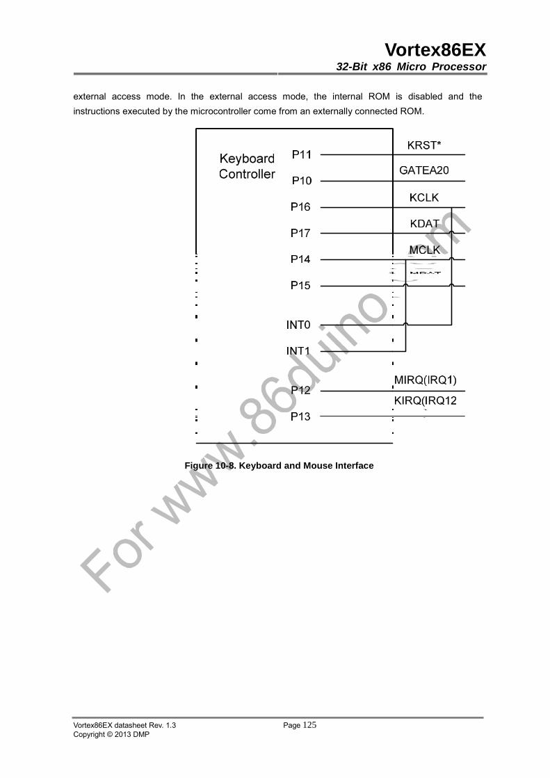
Vortex86EX32-Bit x86 Micro Processor
Vortex86EX datasheet Rev. 1.3 Page 125Copyright © 2013 DMP
external access mode. In the external access mode, the internal ROM is disabled and the
instructions executed by the microcontroller come from an externally connected ROM.
Figure 10-8. Keyboard and Mouse Interface
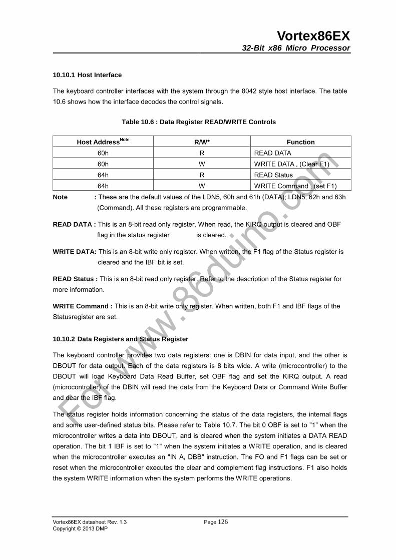
Vortex86EX32-Bit x86 Micro Processor
Vortex86EX datasheet Rev. 1.3 Page 126Copyright © 2013 DMP
10.10.1 Host Interface
The keyboard controller interfaces with the system through the 8042 style host interface. The table
10.6 shows how the interface decodes the control signals.
Table 10.6 : Data Register READ/WRITE Controls
Note : These are the default values of the LDN5, 60h and 61h (DATA); LDN5, 62h and 63h
(Command). All these registers are programmable.
READ DATA : This is an 8-bit read only register. When read, the KIRQ output is cleared and OBF
flag in the status register is cleared.
WRITE DATA: This is an 8-bit write only register. When written, the F1 flag of the Status register is
cleared and the IBF bit is set.
READ Status : This is an 8-bit read only register. Refer to the description of the Status register for
more information.
WRITE Command : This is an 8-bit write only register. When written, both F1 and IBF flags of the
Statusregister are set.
10.10.2 Data Registers and Status Register
The keyboard controller provides two data registers: one is DBIN for data input, and the other is
DBOUT for data output. Each of the data registers is 8 bits wide. A write (microcontroller) to the
DBOUT will load Keyboard Data Read Buffer, set OBF flag and set the KIRQ output. A read
(microcontroller) of the DBIN will read the data from the Keyboard Data or Command Write Buffer
and dear the IBF flag.
The status register holds information concerning the status of the data registers, the internal flags
and some user-defined status bits. Please refer to Table 10.7. The bit 0 OBF is set to "1" when the
microcontroller writes a data into DBOUT, and is cleared when the system initiates a DATA READ
operation. The bit 1 IBF is set to "1" when the system initiates a WRITE operation, and is cleared
when the microcontroller executes an "IN A, DBB" instruction. The FO and F1 flags can be set or
reset when the microcontroller executes the clear and complement flag instructions. F1 also holds
the system WRITE information when the system performs the WRITE operations.
Host AddressNote R/W* Function
60h R READ DATA
60h W WRITE DATA , (Clear F1)
64h R READ Status
64h W WRITE Command , (set F1)
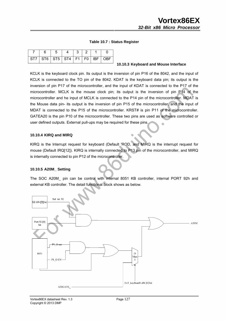
Vortex86EX32-Bit x86 Micro Processor
Vortex86EX datasheet Rev. 1.3 Page 127Copyright © 2013 DMP
Table 10.7 : Status Register
10.10.3 Keyboard and Mouse Interface
KCLK is the keyboard clock pin. Its output is the inversion of pin P16 of the 8042, and the input of
KCLK is connected to the TO pin of the 8042. KDAT is the keyboard data pin; its output is the
inversion of pin P17 of the microcontroller, and the input of KDAT is connected to the P17 of the
microcontroller. MCLK is the mouse clock pin; its output is the inversion of pin P14 of the
microcontroller and he input of MCLK is connected to the P14 pin of the microcontroller. MDAT is
the Mouse data pin- its output is the inversion of pin P15 of the microcontroller, and the input of
MDAT is connected to the P15 of the microcontroller. KRST# is pin P11 of the microcontroller.
GATEA20 is the pin P10 of the microcontroller. These two pins are used as software controlled or
user defined outputs. External pull-ups may be required for these pins.
10.10.4 KIRQ and MlRQ
KIRQ is the lnterrupt request for keyboard (Default 'ROD, and MIRQ is the interrupt request for
mouse (Default IRQ[12]). KIRQ is internally connected to P13 pin of the microcontroller, and MIRQ
is internally connected to pin P12 of the microcontroller.
10.10.5 A20M_ Setting
The SOC A20M_ pin can be control with internal 8051 KB controller, internal PORT 92h and
external KB controller. The detail functional block shows as below.
7 6 5 4 3 2 1 0
ST7 ST6 ST5 ST4 F1 F0 IBF OBF
Vortex86EX32-Bit x86 Micro Processor
Vortex86EX datasheet Rev. 1.3 Page 128Copyright © 2013 DMP
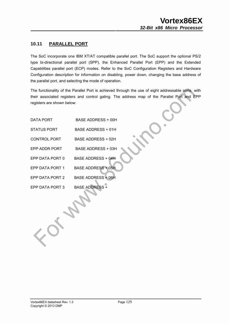
Vortex86EX32-Bit x86 Micro Processor
Vortex86EX datasheet Rev. 1.3 Page 129Copyright © 2013 DMP
10.11 PARALLEL PORT
The SoC incorporate one IBM XT/AT compatible parallel port. The SoC support the optional PS/2
type bi-directional parallel port (SPP), the Enhanced Parallel Port (EPP) and the Extended
Capabilities parallel port (ECP) modes. Refer to the SoC Configuration Registers and Hardware
Configuration description for information on disabling, power down, changing the base address of
the parallel port, and selecting the mode of operation.
The functionality of the Parallel Port is achieved through the use of eight addressable ports, with
their associated registers and control gating. The address map of the Parallel Port and EPP
registers are shown below:
DATA PORT BASE ADDRESS + 00H
STATUS PORT BASE ADDRESS + 01H
CONTROL PORT BASE ADDRESS + 02H
EPP ADDR PORT BASE ADDRESS + 03H
EPP DATA PORT 0 BASE ADDRESS + 04H
EPP DATA PORT 1 BASE ADDRESS + 05H
EPP DATA PORT 2 BASE ADDRESS + 06H
EPP DATA PORT 3 BASE ADDRESS +
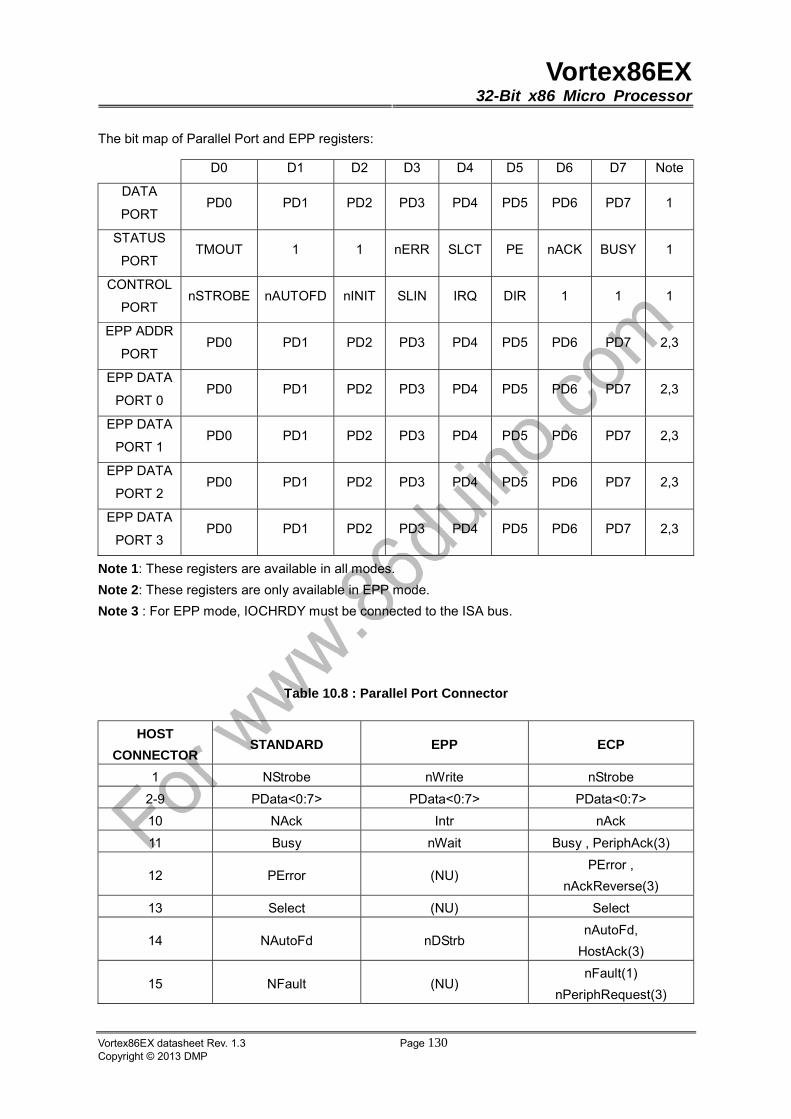
Vortex86EX32-Bit x86 Micro Processor
Vortex86EX datasheet Rev. 1.3 Page 130Copyright © 2013 DMP
The bit map of Parallel Port and EPP registers:
D0 D1 D2 D3 D4 D5 D6 D7 Note
DATA
PORT PD0 PD1 PD2 PD3 PD4 PD5 PD6 PD7 1
STATUS
PORT TMOUT 1 1 nERR SLCT PE nACK BUSY 1
CONTROL
PORT nSTROBE nAUTOFD nINIT SLIN IRQ DIR 1 1 1
EPP ADDR
PORT PD0 PD1 PD2 PD3 PD4 PD5 PD6 PD7 2,3
EPP DATA
PORT 0 PD0 PD1 PD2 PD3 PD4 PD5 PD6 PD7 2,3
EPP DATA
PORT 1 PD0 PD1 PD2 PD3 PD4 PD5 PD6 PD7 2,3
EPP DATA
PORT 2 PD0 PD1 PD2 PD3 PD4 PD5 PD6 PD7 2,3
EPP DATA
PORT 3 PD0 PD1 PD2 PD3 PD4 PD5 PD6 PD7 2,3
Note 1: These registers are available in all modes.
Note 2: These registers are only available in EPP mode.
Note 3 : For EPP mode, IOCHRDY must be connected to the ISA bus.
Table 10.8 : Parallel Port Connector
HOST
CONNECTOR STANDARD EPP ECP
1 NStrobe nWrite nStrobe
2-9 PData<0:7> PData<0:7> PData<0:7>
10 NAck Intr nAck
11 Busy nWait Busy , PeriphAck(3)
12 PError (NU) PError ,
nAckReverse(3)
13 Select (NU) Select
14 NAutoFd nDStrb nAutoFd,
HostAck(3)
15 NFault (NU) nFault(1)
nPeriphRequest(3)
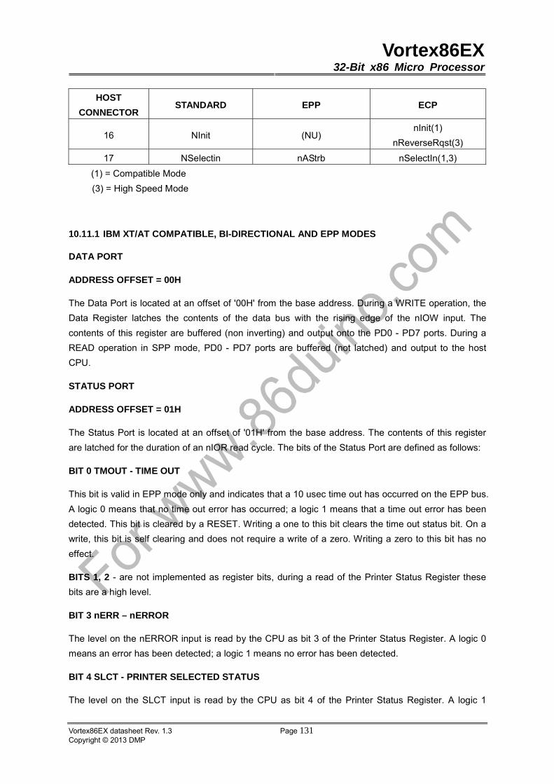
Vortex86EX32-Bit x86 Micro Processor
Vortex86EX datasheet Rev. 1.3 Page 131Copyright © 2013 DMP
HOST
CONNECTOR STANDARD EPP ECP
16 NInit (NU) nInit(1)
nReverseRqst(3)
17 NSelectin nAStrb nSelectIn(1,3)
(1) = Compatible Mode
(3) = High Speed Mode
10.11.1 IBM XT/AT COMPATIBLE, BI-DIRECTIONAL AND EPP MODES
DATA PORT
ADDRESS OFFSET = 00H
The Data Port is located at an offset of '00H' from the base address. During a WRITE operation, the
Data Register latches the contents of the data bus with the rising edge of the nIOW input. The
contents of this register are buffered (non inverting) and output onto the PD0 - PD7 ports. During a
READ operation in SPP mode, PD0 - PD7 ports are buffered (not latched) and output to the host
CPU.
STATUS PORT
ADDRESS OFFSET = 01H
The Status Port is located at an offset of '01H' from the base address. The contents of this register
are latched for the duration of an nIOR read cycle. The bits of the Status Port are defined as follows:
BIT 0 TMOUT - TIME OUT
This bit is valid in EPP mode only and indicates that a 10 usec time out has occurred on the EPP bus.
A logic 0 means that no time out error has occurred; a logic 1 means that a time out error has been
detected. This bit is cleared by a RESET. Writing a one to this bit clears the time out status bit. On a
write, this bit is self clearing and does not require a write of a zero. Writing a zero to this bit has no
effect.
BITS 1, 2 - are not implemented as register bits, during a read of the Printer Status Register these
bits are a high level.
BIT 3 nERR – nERROR
The level on the nERROR input is read by the CPU as bit 3 of the Printer Status Register. A logic 0
means an error has been detected; a logic 1 means no error has been detected.
BIT 4 SLCT - PRINTER SELECTED STATUS
The level on the SLCT input is read by the CPU as bit 4 of the Printer Status Register. A logic 1
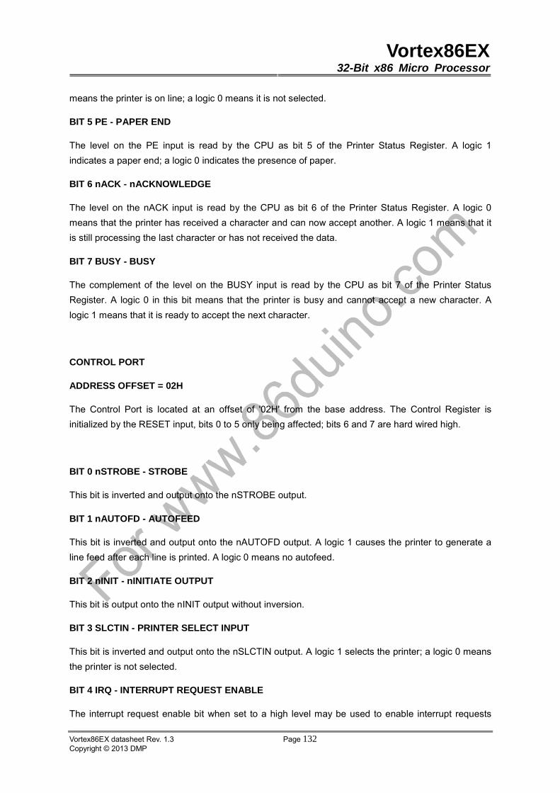
Vortex86EX32-Bit x86 Micro Processor
Vortex86EX datasheet Rev. 1.3 Page 132Copyright © 2013 DMP
means the printer is on line; a logic 0 means it is not selected.
BIT 5 PE - PAPER END
The level on the PE input is read by the CPU as bit 5 of the Printer Status Register. A logic 1
indicates a paper end; a logic 0 indicates the presence of paper.
BIT 6 nACK - nACKNOWLEDGE
The level on the nACK input is read by the CPU as bit 6 of the Printer Status Register. A logic 0
means that the printer has received a character and can now accept another. A logic 1 means that it
is still processing the last character or has not received the data.
BIT 7 BUSY - BUSY
The complement of the level on the BUSY input is read by the CPU as bit 7 of the Printer Status
Register. A logic 0 in this bit means that the printer is busy and cannot accept a new character. A
logic 1 means that it is ready to accept the next character.
CONTROL PORT
ADDRESS OFFSET = 02H
The Control Port is located at an offset of '02H' from the base address. The Control Register is
initialized by the RESET input, bits 0 to 5 only being affected; bits 6 and 7 are hard wired high.
BIT 0 nSTROBE - STROBE
This bit is inverted and output onto the nSTROBE output.
BIT 1 nAUTOFD - AUTOFEED
This bit is inverted and output onto the nAUTOFD output. A logic 1 causes the printer to generate a
line feed after each line is printed. A logic 0 means no autofeed.
BIT 2 nINIT - nINITIATE OUTPUT
This bit is output onto the nINIT output without inversion.
BIT 3 SLCTIN - PRINTER SELECT INPUT
This bit is inverted and output onto the nSLCTIN output. A logic 1 selects the printer; a logic 0 means
the printer is not selected.
BIT 4 IRQ - INTERRUPT REQUEST ENABLE
The interrupt request enable bit when set to a high level may be used to enable interrupt requests
Vortex86EX32-Bit x86 Micro Processor
Vortex86EX datasheet Rev. 1.3 Page 133Copyright © 2013 DMP
from the Parallel Port to the CPU. An interrupt request is generated on the IRQ port by a positive
going nACK input. When the IRQE bit is programmed low the IRQ is disabled.
BIT 5 DIR - PARALLEL CONTROL DIRECTION Parallel Control Direction is valid in extended mode.
In printer mode, the direction is always out regardless of the state of this bit. In bi-directional mode, a
logic 0 means that the printer port is in output mode (write); a logic 1 means that the printer port is in
input mode (read).
Bits 6 and 7 during a read are a high level, and cannot be written.
EPP ADDRESS PORT
ADDRESS OFFSET = 03H
The EPP Address Port is located at an offset of '03H' from the base address. During a WRITE
operation, the contents of DB0 - DB7 are buffered (non inverting) and output onto the PD0 - PD7
ports, the leading edge of nIOW causes an EPP ADDRESS WRITE cycle to be performed, the
trailing edge of IOW latches the data for the duration of the EPP write cycle. During a READ
operation, PD0 - PD7 ports are read, the leading edge of IOR causes an EPP ADDRESS READ
cycle to be performed and the data output to the host CPU, the deassertion of ADDRSTB latches the
PData for the duration of the IOR cycle. This register is only available in EPP mode.
EPP DATA PORT 0
ADDRESS OFFSET = 04H
The EPP Data Port 0 is located at an offset of '04H' from the base address. During a WRITE
operation, the contents of DB0-DB7 are buffered (non inverting) and output onto the PD0 - PD7 ports,
the leading edge of nIOW causes an EPP DATA WRITE cycle to be performed, the trailing edge of
IOW latches the data for the duration of the EPP write cycle. During a READ operation, PD0 - PD7
ports are read, the leading edge of IOR causes an EPP READ cycle to be performed and the data
output to the host CPU, the deassertion of DATASTB latches the PData for the duration of the IOR
cycle. This register is only available in EPP mode.
EPP DATA PORT 1
ADDRESS OFFSET = 05H
The EPP Data Port 1 is located at an offset of '05H' from the base address. Refer to EPP DATA
PORT 0 for a description of operation. This register is only available in EPP mode.
EPP DATA PORT 2
ADDRESS OFFSET = 06H
The EPP Data Port 2 is located at an offset of '06H' from the base address. Refer to EPP DATA

Vortex86EX32-Bit x86 Micro Processor
Vortex86EX datasheet Rev. 1.3 Page 134Copyright © 2013 DMP
PORT 0 for a description of operation. This register is only available in EPP mode.
EPP DATA PORT 3
ADDRESS OFFSET = 07H
The EPP Data Port 3 is located at an offset of '07H' from the base address. Refer to EPP DATA
PORT 0 for a description of operation. This register is only available in EPP mode.
EPP 1.9 OPERATION
When the EPP mode is selected in the configuration register, the standard and bidirectional modes
are also available. If no EPP Read, Write or Address cycle is currently executing, then the PDx bus is
in the standard or bi-directional mode, and all output signals (nSTROBE, nAUTOFD, nINIT) are as
set by the SPP Control Port and direction is controlled by DIR of the Control port.
In EPP mode, the system timing is closely coupled to the EPP timing. For this reason, a watchdog
timer is required to prevent system lockup. The timer indicates if more than 10usec have elapsed
from the start of the EPP cycle (nIOR or nIOW asserted) to nWAIT being deasserted (after
command). If a time-out occurs, the current EPP cycle is aborted and the time-out condition is
indicated in Status bit 0.
During an EPP cycle, if nSTROBE is active, it overrides the EPP write signal forcing the PDx bus to
always be in a write mode and the nWRITE signal to always be asserted.
Software Constraints
Before an EPP cycle is executed, the software must ensure that the control register bit DIR is a logic
"0" (ie a 04H or 05H should be written to the Control port). If the user leaves DIR as a logic "1", and
attempts to perform an EPP write, the chip is unable to perform the write (because DIR is a logic "1")
and will appear to perform an EPP read on the parallel bus, no error is indicated.
EPP 1.9 Write
The timing for a write operation (address or data) is shown in timing diagram EPP1.9 Write Data or
Address cycle. IOCHRDY is driven active low at the start of each EPP write and is released when it
has been determined that the write cycle can complete. The write cycle can complete under the
following circumstances:
1. If the EPP bus is not ready (nWAIT is active low) when nDATASTB or nADDRSTB goes active
then the write can complete
when nWAIT goes inactive high.
2. If the EPP bus is ready (nWAIT is inactive high) then the chip must wait for it to go active low
before changing the state of
nDATASTB, nWRITE or nADDRSTB. The write can complete once nWAIT is determined inactive.

Vortex86EX32-Bit x86 Micro Processor
Vortex86EX datasheet Rev. 1.3 Page 135Copyright © 2013 DMP
Write Sequence of operation
1. The host selects an EPP register, places data on the SData bus and drives nIOW active.
2. The chip drives IOCHRDY inactive (low).
3. If WAIT is not asserted, the chip must wait until WAIT is asserted.
4. The chip places address or data on PData bus, clears PDIR, and asserts nWRITE.
5. Chip asserts nDATASTB or nADDRSTRB indicating that PData bus contains valid information, and
the WRITE signal is valid.
6. Peripheral deasserts nWAIT, indicating that any setup requirements have been satisfied and the
chip may begin the
termination phase of the cycle.
7. a) The chip deasserts nDATASTB or nADDRSTRB, this marks the beginning of the termination
phase. If it has not already done so, the peripheral should latch the information byte now.
b) The chip latches the data from the SData bus for the PData bus and asserts (releases) IOCHRDY
allowing the host to complete the write cycle.
8. Peripheral asserts nWAIT, indicating to the host that any hold time requirements have been
satisfied and acknowledging the termination of the cycle.
9. Chip may modify nWRITE and nPDATA in preparation for the next cycle.
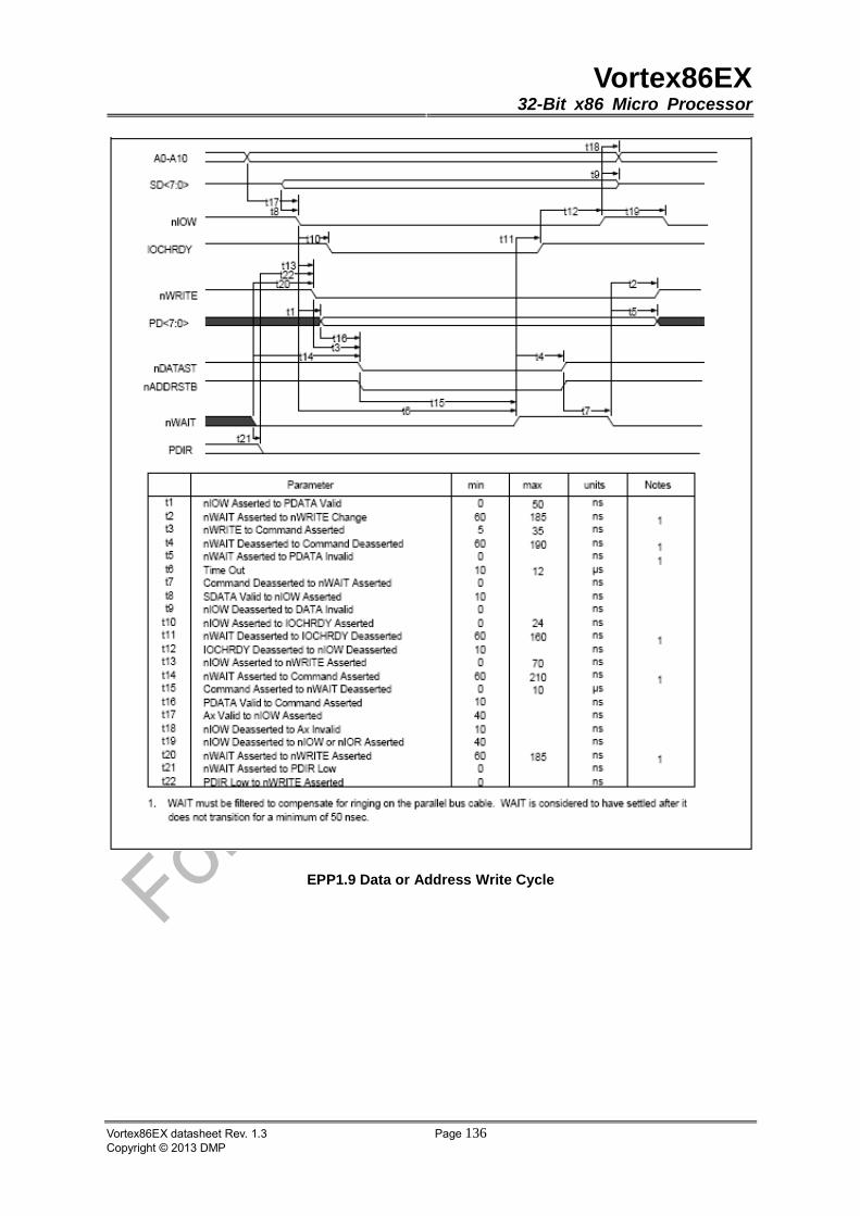
Vortex86EX32-Bit x86 Micro Processor
Vortex86EX datasheet Rev. 1.3 Page 136Copyright © 2013 DMP
EPP1.9 Data or Address Write Cycle
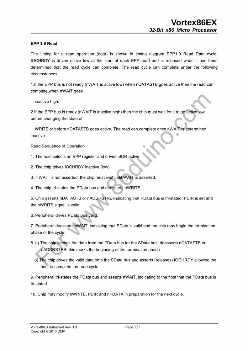
Vortex86EX32-Bit x86 Micro Processor
Vortex86EX datasheet Rev. 1.3 Page 137Copyright © 2013 DMP
EPP 1.9 Read
The timing for a read operation (data) is shown in timing diagram EPP1.9 Read Data cycle.
IOCHRDY is driven active low at the start of each EPP read and is released when it has been
determined that the read cycle can complete. The read cycle can complete under the following
circumstances:
1.If the EPP bus is not ready (nWAIT is active low) when nDATASTB goes active then the read can
complete when nWAIT goes
inactive high.
2.If the EPP bus is ready (nWAIT is inactive high) then the chip must wait for it to go active low
before changing the state of
WRITE or before nDATASTB goes active. The read can complete once nWAIT is determined
inactive.
Read Sequence of Operation
1. The host selects an EPP register and drives nIOR active.
2. The chip drives IOCHRDY inactive (low).
3. If WAIT is not asserted, the chip must wait until WAIT is asserted.
4. The chip tri-states the PData bus and deasserts nWRITE.
5. Chip asserts nDATASTB or nADDRSTRB indicating that PData bus is tri-stated, PDIR is set and
the nWRITE signal is valid.
6. Peripheral drives PData bus valid.
7. Peripheral deasserts nWAIT, indicating that PData is valid and the chip may begin the termination
phase of the cycle.
8. a) The chip latches the data from the PData bus for the SData bus, deasserts nDATASTB or
nADDRSTRB, this marks the beginning of the termination phase.
b) The chip drives the valid data onto the SData bus and asserts (releases) IOCHRDY allowing the
host to complete the read cycle.
9. Peripheral tri-states the PData bus and asserts nWAIT, indicating to the host that the PData bus is
tri-stated.
10. Chip may modify nWRITE, PDIR and nPDATA in preparation for the next cycle.
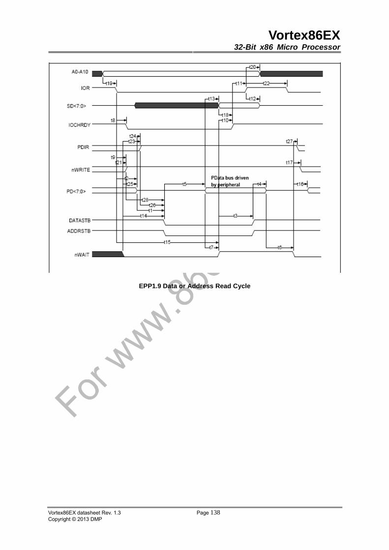
Vortex86EX32-Bit x86 Micro Processor
Vortex86EX datasheet Rev. 1.3 Page 138Copyright © 2013 DMP
EPP1.9 Data or Address Read Cycle

Vortex86EX32-Bit x86 Micro Processor
Vortex86EX datasheet Rev. 1.3 Page 139Copyright © 2013 DMP
EPP1.9 Data or Address Read Cycle Timing Parameter
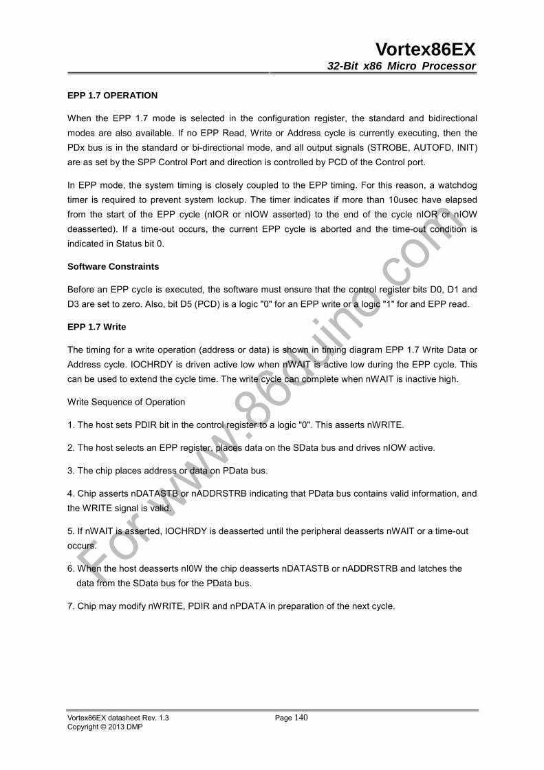
Vortex86EX32-Bit x86 Micro Processor
Vortex86EX datasheet Rev. 1.3 Page 140Copyright © 2013 DMP
EPP 1.7 OPERATION
When the EPP 1.7 mode is selected in the configuration register, the standard and bidirectional
modes are also available. If no EPP Read, Write or Address cycle is currently executing, then the
PDx bus is in the standard or bi-directional mode, and all output signals (STROBE, AUTOFD, INIT)
are as set by the SPP Control Port and direction is controlled by PCD of the Control port.
In EPP mode, the system timing is closely coupled to the EPP timing. For this reason, a watchdog
timer is required to prevent system lockup. The timer indicates if more than 10usec have elapsed
from the start of the EPP cycle (nIOR or nIOW asserted) to the end of the cycle nIOR or nIOW
deasserted). If a time-out occurs, the current EPP cycle is aborted and the time-out condition is
indicated in Status bit 0.
Software Constraints
Before an EPP cycle is executed, the software must ensure that the control register bits D0, D1 and
D3 are set to zero. Also, bit D5 (PCD) is a logic "0" for an EPP write or a logic "1" for and EPP read.
EPP 1.7 Write
The timing for a write operation (address or data) is shown in timing diagram EPP 1.7 Write Data or
Address cycle. IOCHRDY is driven active low when nWAIT is active low during the EPP cycle. This
can be used to extend the cycle time. The write cycle can complete when nWAIT is inactive high.
Write Sequence of Operation
1. The host sets PDIR bit in the control register to a logic "0". This asserts nWRITE.
2. The host selects an EPP register, places data on the SData bus and drives nIOW active.
3. The chip places address or data on PData bus.
4. Chip asserts nDATASTB or nADDRSTRB indicating that PData bus contains valid information, and
the WRITE signal is valid.
5. If nWAIT is asserted, IOCHRDY is deasserted until the peripheral deasserts nWAIT or a time-out
occurs.
6. When the host deasserts nI0W the chip deasserts nDATASTB or nADDRSTRB and latches the
data from the SData bus for the PData bus.
7. Chip may modify nWRITE, PDIR and nPDATA in preparation of the next cycle.
Vortex86EX32-Bit x86 Micro Processor
Vortex86EX datasheet Rev. 1.3 Page 141Copyright © 2013 DMP
EPP 1.7 Data or Address Write Cycle
Vortex86EX32-Bit x86 Micro Processor
Vortex86EX datasheet Rev. 1.3 Page 142Copyright © 2013 DMP
EPP 1.7 Read
The timing for a read operation (data) is shown in timing diagram EPP 1.7 Read Data cycle.
IOCHRDY is driven active low when nWAIT is active low during the EPP cycle. This can be used to
extend the cycle time. The read cycle can complete when nWAIT is inactive high.
Read Sequence of Operation
1. The host sets PDIR bit in the control register to a logic "1". This deasserts nWRITE and tri-states
the PData bus.
2. The host selects an EPP register and drives nIOR active.
3. Chip asserts nDATASTB or nADDRSTRB indicating that PData bus is tri-stated, PDIR is set and
the nWRITE signal is valid.
4. If nWAIT is asserted, IOCHRDY is deasserted until the peripheral deasserts nWAIT or a time-out
occurs.
5. The Peripheral drives PData bus valid.
6. The Peripheral deasserts nWAIT, indicating that PData is valid and the chip may begin the
termination phase of the cycle.
7. When the host deasserts nI0R the chip deasserts nDATASTB or nADDRSTRB.
8. Peripheral tri-states the PData bus.
9. Chip may modify nWRITE, PDIR andnPDATA in preparation of the next cycle.

Vortex86EX32-Bit x86 Micro Processor
Vortex86EX datasheet Rev. 1.3 Page 143Copyright © 2013 DMP
EPP 1.7 Data or Address Read Cycle
Vortex86EX32-Bit x86 Micro Processor
Vortex86EX datasheet Rev. 1.3 Page 144Copyright © 2013 DMP
Table 10.9 : EPP Pin Descriptions
EPP
Signal EPP NAME TYPE EPP DESCRIPTION
nWRITE nWrite O This signal is active low. It denotes a write operation.
PD<0:7> Address/Data I/O Bi-directional EPP byte wide address and data bus.
INTR Interrupt I This signal is active high and positive edge triggered.
(Pass
through with no inversion, Same as SPP.)
nWAIT nWait I This signal is active low. It is driven inactive as a positive
acknowledgement from the device that the transfer of
data
is completed. It is driven active as an indication that the
device is ready for the next transfer.
nDATASTB nData Strobe O This signal is active low. It is used to denote data read or
write operation.
nRESET nReset O This signal is active low. When driven active, the EPP
device is reset to its initial operational mode.
nADDRSTB nAddress
Strobe
O This signal is active low. It is used to denote address
read or write operation.
PE Paper End I Same as SPP mode.
SLCT Printer
Selected
Status
I Same as SPP mode.
Nerr nError I Same as SPP mode.
DIR Parallel Port
Direction
O This output shows the direction of the data transfer on the
parallel port bus. A low means an output/write condition
and a high means an input/read condition. This signal is
normally a low (output/write) unless PCD of the control
register is set or if an EPP read cycle is in progress.
Note 1: SPP and EPP can use 1 common register.
Note 2: nWrite is the only EPP output that can be over-ridden by SPP control port during an EPP
cycle. For correct EPP read cycles, DIR is required to be a low.
Vortex86EX32-Bit x86 Micro Processor
Vortex86EX datasheet Rev. 1.3 Page 145Copyright © 2013 DMP
10.11.2 EXTENDED CAPABILITIES PARALLEL PORT
ECP provides a number of advantages, some of which are listed below. The individual features are
explained in greater detail in the remainderof this section.
� High performance half-duplex forward andreverse channel
� Interlocked handshake, for fast reliable transfer
� Channel addressing for low-cost peripherals
� Maintains link and data layer separation
� Permits the use of active output drivers
� Permits the use of adaptive signal timing
� Peer-to-peer capability
Vocabulary
The following terms are used in this document:
assert: When a signal asserts it transitions to a "true" state, when a signal deasserts it transitions to
a "false" state.
forward: Host to Peripheral communication.
reverse: Peripheral to Host communication.
PWord: A port word; equal in size to the width of the ISA interface. For this implementation, PWord
is always 8 bits.
1: A high level.
0: A low level.
These terms may be considered synonymous:
� PeriphClk, nAck
� HostAck, nAutoFd
� PeriphAck, Busy
� nPeriphRequest, nFault
� nReverseRequest, nInit
� nAckReverse, PError
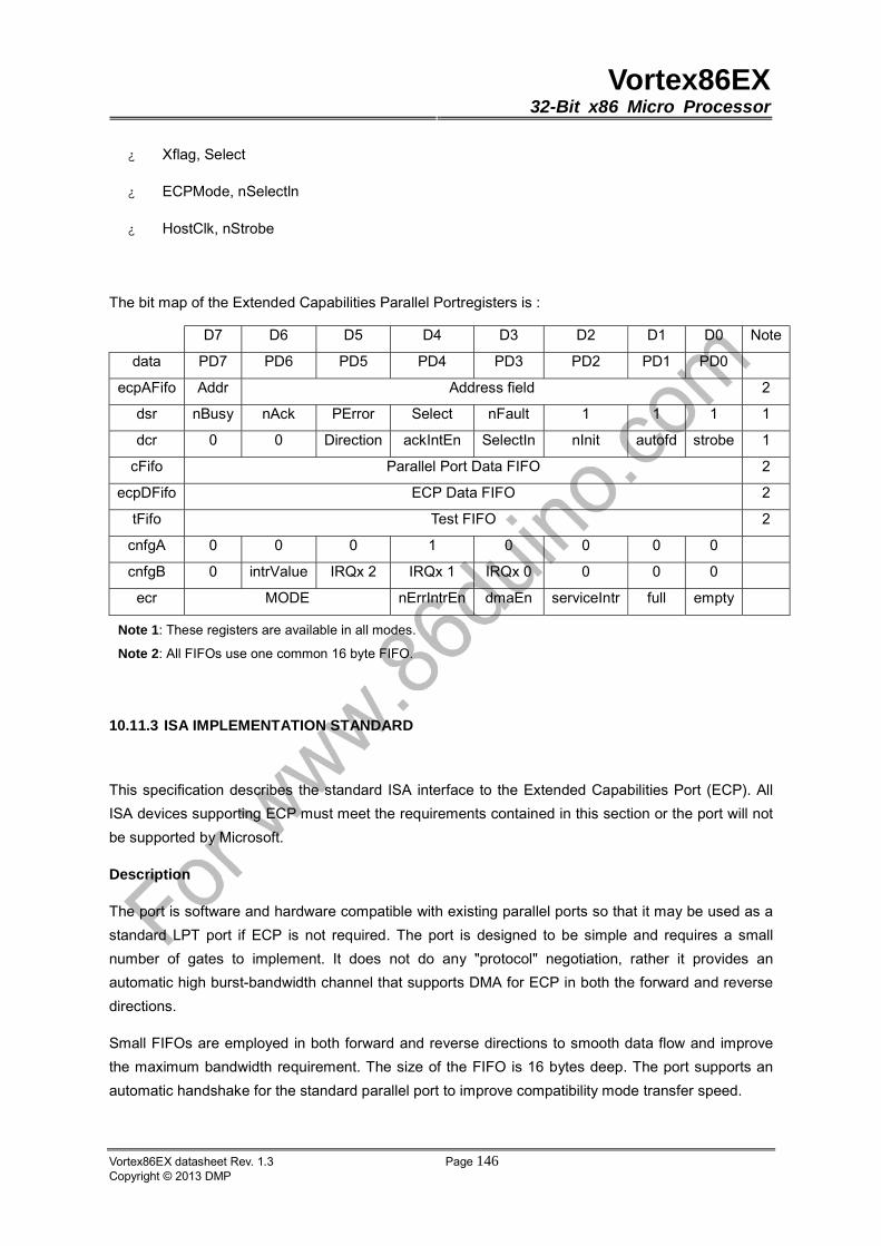
Vortex86EX32-Bit x86 Micro Processor
Vortex86EX datasheet Rev. 1.3 Page 146Copyright © 2013 DMP
� Xflag, Select
� ECPMode, nSelectln
� HostClk, nStrobe
The bit map of the Extended Capabilities Parallel Portregisters is :
D7 D6 D5 D4 D3 D2 D1 D0 Note
data PD7 PD6 PD5 PD4 PD3 PD2 PD1 PD0
ecpAFifo Addr Address field 2
dsr nBusy nAck PError Select nFault 1 1 1 1
dcr 0 0 Direction ackIntEn SelectIn nInit autofd strobe 1
cFifo Parallel Port Data FIFO 2
ecpDFifo ECP Data FIFO 2
tFifo Test FIFO 2
cnfgA 0 0 0 1 0 0 0 0
cnfgB 0 intrValue IRQx 2 IRQx 1 IRQx 0 0 0 0
ecr MODE nErrIntrEn dmaEn serviceIntr full empty
Note 1: These registers are available in all modes.
Note 2: All FIFOs use one common 16 byte FIFO.
10.11.3 ISA IMPLEMENTATION STANDARD
This specification describes the standard ISA interface to the Extended Capabilities Port (ECP). All
ISA devices supporting ECP must meet the requirements contained in this section or the port will not
be supported by Microsoft.
Description
The port is software and hardware compatible with existing parallel ports so that it may be used as a
standard LPT port if ECP is not required. The port is designed to be simple and requires a small
number of gates to implement. It does not do any "protocol" negotiation, rather it provides an
automatic high burst-bandwidth channel that supports DMA for ECP in both the forward and reverse
directions.
Small FIFOs are employed in both forward and reverse directions to smooth data flow and improve
the maximum bandwidth requirement. The size of the FIFO is 16 bytes deep. The port supports an
automatic handshake for the standard parallel port to improve compatibility mode transfer speed.
Vortex86EX32-Bit x86 Micro Processor
Vortex86EX datasheet Rev. 1.3 Page 147Copyright © 2013 DMP
Table 10.10 : ECP Pin Descriptions
NAME TYPE DESCRIPTION
nStrobe O
During write operations nStrobe registers data or address into
the slave
on the asserting edge (handshakes with Busy).
PData 7:0 I/O Contains address or data.
nAck I
Indicates valid data driven by the peripheral when asserted.
This signal
handshakes with nAutoFd in reverse.
PeriphAck (Busy) I
This signal deasserts to indicate that the peripheral can accept
data.
This signal handshakes with nStrobe in the forward direction.
In the
reverse direction this signal indicates whether the data lines
contain
ECP command information or data. The peripheral uses this
signal to
flow control in the forward direction. It is an "interlocked"
handshake
with nStrobe. PeriphAck also provides command information
in the
reverse direction.
PError
(nAckReverse) I
Used to acknowledge a change in the direction the transfer
(asserted =
forward). The peripheral drives this signal low to acknowledge
nReverseRequest. It is an "interlocked" handshake with
nReverseRequest. The host relies upon nAckReverse to
determine
when it is permitted to drive the data bus.
Select I Indicates printer on line.
nAutoFd
(HostAck) O
Requests a byte of data from the peripheral when asserted,
handshaking with nAck in the reverse direction. In the forward
direction
this signal indicates whether the data lines contain ECP
address or
data. The host drives this signal to flow control in the reverse
direction.
It is an "interlocked" handshake with Ack. HostAck also
provides
command information in the forward phase.
Vortex86EX32-Bit x86 Micro Processor
Vortex86EX datasheet Rev. 1.3 Page 148Copyright © 2013 DMP
NAME TYPE DESCRIPTION
nFault
(nPeriphRequest) I
Generates an error interrupt when asserted. This signal
provides a
mechanism for peer-to-peer communication. This signal is
valid only in
the forward direction. During ECP Mode the peripheral is
permitted
(but not required) to drive this pin low to request a reverse
transfer. The
request is merely a "hint" to the host; the host has ultimate
control over
the transfer direction. This signal would be typically used to
generate
an interrupt to the host CPU.
nInit O
Sets the transfer direction (asserted = reverse, deasserted =
forward).
This pin is driven low to place the channel in the reverse
direction. The
peripheral is only allowed to drive the bi-directional data bus
while in
ECP Mode and HostAck is low and nSelectIn is high.
nSelectIn O Always deasserted in ECP mode.
Register Definitions
The register definitions are based on the standard IBM addresses for LPT. All of the standard printer
ports are supported. The additional registers attach to an upper bit decode of the standard LPT port
definition to avoid conflict with standard ISA devices. The port is equivalent to a generic parallel port
interface and may be operated in that mode. The port registers vary depending on the mode field in
the ecr. The table below lists these dependencies. Operation of the devices in modes other that
those specified is undefined.
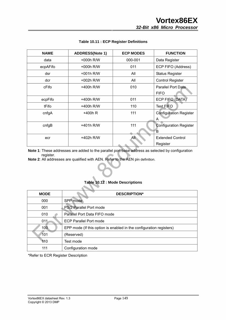
Vortex86EX32-Bit x86 Micro Processor
Vortex86EX datasheet Rev. 1.3 Page 149Copyright © 2013 DMP
Table 10.11 : ECP Register Definitions
NAME ADDRESS(Note 1) ECP MODES FUNCTION
data +000h R/W 000-001 Data Register
ecpAFifo +000h R/W 011 ECP FIFO (Address)
dsr +001h R/W All Status Register
dcr +002h R/W All Control Register
cFifo +400h R/W 010 Parallel Port Data
FIFO
ecpFifo +400h R/W 011 ECP FIFO (DATA)
tFifo +400h R/W 110 Test FIFO
cnfgA +400h R 111 Configuration Register
A
cnfgB +401h R/W 111 Configuration Register
B
ecr +402h R/W All Extended Control
Register
Note 1: These addresses are added to the parallel port base address as selected by configuration register.
Note 2: All addresses are qualified with AEN. Refer to the AEN pin definition.
Table 10.12 : Mode Descriptions
MODE DESCRIPTION*
000 SPP mode
001 PS/2 Parallel Port mode
010 Parallel Port Data FIFO mode
011 ECP Parallel Port mode
100 EPP mode (If this option is enabled in the configuration registers)
101 (Reserved)
110 Test mode
111 Configuration mode
*Refer to ECR Register Description
Vortex86EX32-Bit x86 Micro Processor
Vortex86EX datasheet Rev. 1.3 Page 150Copyright © 2013 DMP
DATA and ecpAFifo PORT
ADDRESS OFFSET = 00H
Modes 000 and 001 (Data Port)
The Data Port is located at an offset of '00H' from the base address. The data register is cleared at
initialization by RESET. During a WRITE operation, the Data Register latches the contents of the
data bus on the rising edge of the nIOW input. The contents of this register are buffered (non
inverting) and output onto the PD0 - PD7 ports. During a READ operation, PD0 - PD7 ports are read
and output to the host CPU.
Mode 011 (ECP FIFO - Address)
A data byte written to this address is placed in the FIFO and tagged as an ECP Address. The
hardware at the ECP port transmits this byte to the peripheral automatically. The operation of this
register is only defined for the forward direction (direction is 0). Refer to the ECP Parallel Port
Forward Timing Diagram, located in the Timing Diagrams section of this data sheet.
DEVICE STATUS REGISTER (dsr)
ADDRESS OFFSET = 01H
The Status Port is located at an offset of '01H' from the base address. Bits 0 - 2 are not implemented
as register bits, during a read of the Printer Status Register these bits are a high level. The bits of the
Status Port are defined as follows:
BIT 3 nFault
The level on the nFault input is read by the CPU as bit 3 of the Device Status Register.
BIT 4 Select
The level on the Select input is read by the CPU as bit 4 of the Device Status Register.
BIT 5 PError
The level on the PError input is read by the CPU as bit 5 of the Device Status Register. Printer Status
Register.
BIT 6 nAck
The level on the nAck input is read by the CPU as bit 6 of the Device Status Register.
BIT 7 nBusy
The complement of the level on the BUSY input is read by the CPU as bit 7 of the Device Status
Register.
Vortex86EX32-Bit x86 Micro Processor
Vortex86EX datasheet Rev. 1.3 Page 151Copyright © 2013 DMP
DEVICE CONTROL REGISTER (dcr)
ADDRESS OFFSET = 02H
The Control Register is located at an offset of '02H' from the base address. The Control Register is
initialized to zero by the RESET input, bits 0 to 5 only being affected; bits 6 and 7 are hard wired
high.
BIT 0 STROBE – STROBE
This bit is inverted and output onto the nSTROBE output.
BIT 1 AUTOFD – AUTOFEED
This bit is inverted and output onto the nAUTOFD output. A logic 1 causes the printer to generate a
line feed after each line is printed. A logic 0 means no autofeed.
BIT 2 nINIT - nINITIATE OUTPUT
This bit is output onto the nINIT output without inversion.
BIT 3 SELECTIN
This bit is inverted and output onto the nSLCTIN output. A logic 1 on this bit selects the printer; a
logic 0 means the printer is not selected.
BIT 4 ackIntEn - INTERRUPT REQUEST ENABLE
The interrupt request enable bit when set to a high level may be used to enable interrupt requests
from the Parallel Port to the CPU due to a low to high transition on the nACK input. Refer to the
description of the interrupt under Operation, Interrupts.
BIT 5 DIRECTION
If mode=000 or mode=010, this bit has no effect and the direction is always out regardless of the
state of this bit. In all other modes, Direction is valid and a logic 0 means that the printer port is in
output mode (write); a logic 1 means that the printer port is in input mode (read).
Bits 6 and 7 during a read are a high level, and cannot be written.
cFifo (Parallel Port Data FIFO)
ADDRESS OFFSET = 400h
Mode = 010
Bytes written or DMAed from the system to this FIFO are transmitted by a hardware handshake to
the peripheral using the standard parallel port protocol. Transfers to the FIFO are byte aligned. This
Vortex86EX32-Bit x86 Micro Processor
Vortex86EX datasheet Rev. 1.3 Page 152Copyright © 2013 DMP
mode is only defined for the forward direction.
ecpDFifo (ECP Data FIFO)
ADDRESS OFFSET = 400H
Mode = 011
Bytes written or DMAed from the system to this FIFO, when the direction bit is 0, are transmitted by a
hardware handshake to the peripheral using the ECP parallel port protocol. Transfers to the FIFO are
byte aligned.
Data bytes from the peripheral are read under automatic hardware handshake from ECP into this
FIFO when the direction bit is 1. Reads or DMAs from the FIFO will return bytes of ECP data to the
system.
tFifo (Test FIFO Mode)
ADDRESS OFFSET = 400H
Mode = 110
Data bytes may be read, written or DMAed to or from the system to this FIFO in any direction. Data in
the tFIFO will not be transmitted to the to the parallel port lines using a hardware protocol handshake.
However, data in the tFIFO may be displayed on the parallel port data lines.
The tFIFO will not stall when overwritten or underrun. If an attempt is made to write data to a full
tFIFO, the new data is not accepted into the tFIFO. If an attempt is made to read data from an empty
tFIFO, the last data byte is reread again. The full and empty bits must always keep track of the
correct FIFO state. The tFIFO will transfer data at the maximum ISA rate so that software may
generate performance metrics.
The FIFO size can be determined by writing bytes to the FIFO and checking the full bit.
Data bytes are always read from the head of tFIFO regardless of the value of the direction bit. For
example if 44h, 33h, 22h is written to the FIFO, then reading the tFIFO will return 44h, 33h, 22h in the
same order as was written.
cnfgA (Configuration Register A)
ADDRESS OFFSET = 400H
Mode = 111
This register is a read only register. When read, 10H is returned. This indicates to the system that
this is an 8-bit implementation. (PWord = 1 byte)
cnfgB (Configuration Register B)
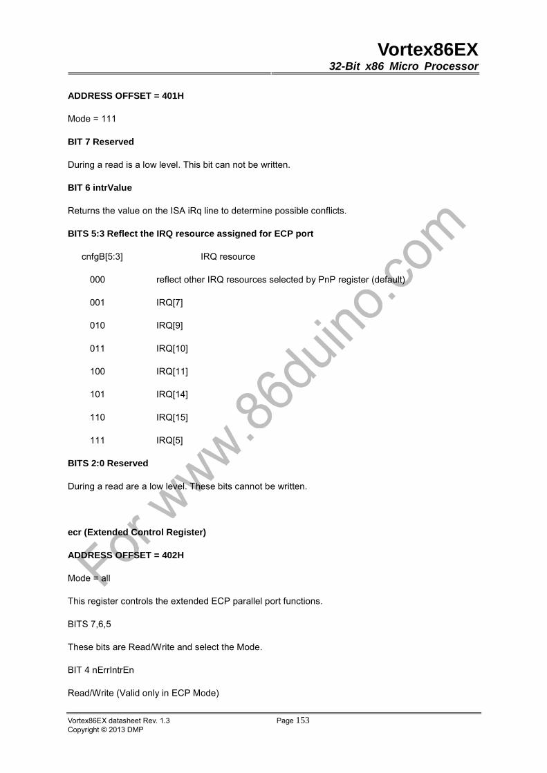
Vortex86EX32-Bit x86 Micro Processor
Vortex86EX datasheet Rev. 1.3 Page 153Copyright © 2013 DMP
ADDRESS OFFSET = 401H
Mode = 111
BIT 7 Reserved
During a read is a low level. This bit can not be written.
BIT 6 intrValue
Returns the value on the ISA iRq line to determine possible conflicts.
BITS 5:3 Reflect the IRQ resource assigned for ECP port
cnfgB[5:3] IRQ resource
000 reflect other IRQ resources selected by PnP register (default)
001 IRQ[7]
010 IRQ[9]
011 IRQ[10]
100 IRQ[11]
101 IRQ[14]
110 IRQ[15]
111 IRQ[5]
BITS 2:0 Reserved
During a read are a low level. These bits cannot be written.
ecr (Extended Control Register)
ADDRESS OFFSET = 402H
Mode = all
This register controls the extended ECP parallel port functions.
BITS 7,6,5
These bits are Read/Write and select the Mode.
BIT 4 nErrIntrEn
Read/Write (Valid only in ECP Mode)

Vortex86EX32-Bit x86 Micro Processor
Vortex86EX datasheet Rev. 1.3 Page 154Copyright © 2013 DMP
1: Disables the interrupt generated on the asserting edge of nFault.
0: Enables an interrupt pulse on the high to low edge of nFault. Note that an interrupt will be
generated if nFault is asserted (interrupting) and this bit is written from a 1 to a 0. This prevents
interrupts from being lost in the time between the read of the ecr and the write of the ecr.
BIT 3 dmaEn
Read/Write
1: Enables DMA (DMA starts when serviceIntr is 0).
0: Disables DMA unconditionally.
BIT 2 serviceIntr
Read/Write
1: Disables DMA and all of the service interrupts.
0: Enables one of the following 3 cases of interrupts. Once one of the 3 service interrupts has
occurred serviceIntr bit shall be set to a 1 by hardware, it must be reset to 0 to re-enable the
interrupts. Writing this bit to a 1 will not cause an interrupt.
case dmaEn=1:
During DMA (this bit is set to a 1 whenterminal count is reached).
case dmaEn=0 direction=0:
This bit shall be set to 1 whenever there are writeIntrThreshold or more bytes free in the FIFO.
case dmaEn=0 direction=1:
This bit shall be set to 1 whenever there are readIntrThreshold or more valid bytes to be read from
the FIFO.
BIT 1 full
Read only
1: The FIFO cannot accept another byte or the FIFO is completely full.
0: The FIFO has at least 1 free byte.
BIT 0 empty
Read only
1: The FIFO is completely empty.
0: The FIFO contains at least 1 byte of data.
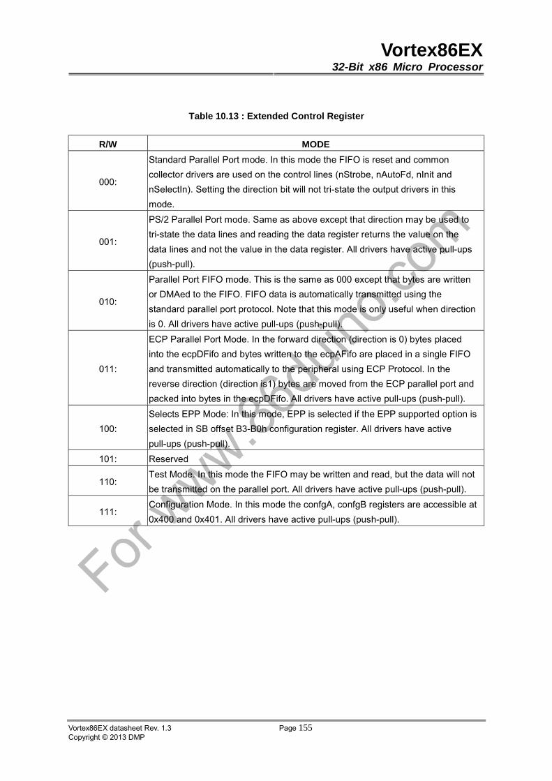
Vortex86EX32-Bit x86 Micro Processor
Vortex86EX datasheet Rev. 1.3 Page 155Copyright © 2013 DMP
Table 10.13 : Extended Control Register
R/W MODE
000:
Standard Parallel Port mode. In this mode the FIFO is reset and common
collector drivers are used on the control lines (nStrobe, nAutoFd, nInit and
nSelectIn). Setting the direction bit will not tri-state the output drivers in this
mode.
001:
PS/2 Parallel Port mode. Same as above except that direction may be used to
tri-state the data lines and reading the data register returns the value on the
data lines and not the value in the data register. All drivers have active pull-ups
(push-pull).
010:
Parallel Port FIFO mode. This is the same as 000 except that bytes are written
or DMAed to the FIFO. FIFO data is automatically transmitted using the
standard parallel port protocol. Note that this mode is only useful when direction
is 0. All drivers have active pull-ups (push-pull).
011:
ECP Parallel Port Mode. In the forward direction (direction is 0) bytes placed
into the ecpDFifo and bytes written to the ecpAFifo are placed in a single FIFO
and transmitted automatically to the peripheral using ECP Protocol. In the
reverse direction (direction is1) bytes are moved from the ECP parallel port and
packed into bytes in the ecpDFifo. All drivers have active pull-ups (push-pull).
100:
Selects EPP Mode: In this mode, EPP is selected if the EPP supported option is
selected in SB offset B3-B0h configuration register. All drivers have active
pull-ups (push-pull).
101: Reserved
110: Test Mode. In this mode the FIFO may be written and read, but the data will not
be transmitted on the parallel port. All drivers have active pull-ups (push-pull).
111: Configuration Mode. In this mode the confgA, confgB registers are accessible at
0x400 and 0x401. All drivers have active pull-ups (push-pull).
Vortex86EX32-Bit x86 Micro Processor
Vortex86EX datasheet Rev. 1.3 Page 156Copyright © 2013 DMP
10.11.4 OPERATION
Mode Switching/Software Control
Software will execute P1284 negotiation and all operation prior to a data transfer phase under programmed I/O control (mode 000 or 001). Hardware provides an automatic control line handshake, moving data between the FIFO and the ECP port only in the data transfer phase (modes 011 or 010).
Setting the mode to 011 or 010 will cause the hardware to initiate data transfer.
If the port is in mode 000 or 001 it may switch to any other mode. If the port is not in mode 000 or 001 it can only
be switched into mode 000 or 001. The direction can only be changed in mode 001.
Once in an extended forward mode the software should wait for the FIFO to be empty before
switching back to mode 000 or 001. In this case all control signals will be deasserted before the
mode switch. In an ecp reverse mode the software waits for all the data to be read from the FIFO
before changing back to mode 000 or 001. Since the automatic hardware ecp reverse handshake
only cares about the state of the FIFO it may have acquired extra data which will be discarded. It may
in fact be in the middle of a transfer when the mode is changed back to 000 or 001. In this case the
port will deassert nAutoFd independent of the state of the transfer. The design shall not cause
glitches on the handshake signals if the software meets the constraints above.
ECP Operation
Prior to ECP operation the Host must negotiate on the parallel port to determine if the peripheral
supports the ECP protocol. This is a somewhat complex negotiation carried out under program
control in mode 000. After negotiation, it is necessary to initialize some of the port bits. The following
are required:
Set Direction = 0, enabling the drivers.
Set strobe = 0, causing the nStrobe signal to default to the deasserted state.
Set autoFd = 0, causing the nAutoFd signal to default to the deasserted state.
Set mode = 011 (ECP Mode)
ECP address bytes or data bytes may be sent automatically by writing the ecpAFifo or ecpDFifo
respectively.
Note that all FIFO data transfers are byte wide and byte aligned. Address transfers are byte-wide and
only allowed in the forward direction.
The host may switch directions by first switching to mode = 001, negotiating for the forward or
reverse channel, setting direction to 1 or 0, then setting mode = 011. When direction is 1 the
hardware shall handshake for each ECP read data byte and attempt to fill the FIFO. Bytes may then
be read from the ecpDFifo as long as it is not empty .
ECP transfers may also be accomplished (albeit slowly) by handshaking individual bytes under
Vortex86EX32-Bit x86 Micro Processor
Vortex86EX datasheet Rev. 1.3 Page 157Copyright © 2013 DMP
program control in mode = 001, or 000.
Termination from ECP Mode
Termination from ECP Mode is similar to the termination from Nibble/Byte Modes. The host is
permitted to terminate from ECP Mode only in specific well-defined states. The termination can only
be executed while the bus is in the forward direction. To terminate while the channel is in the reverse
direction, it must first be transitioned into the forward direction.
Command/Data
ECP Mode supports two advanced features to improve the effectiveness of the protocol for some
applications. The features are implemented by allowing the transfer of normal 8-bit data or 8-bit
commands.
When in the forward direction, normal data is transferred when HostAck is high and an 8-bit
command is transferred when HostAck is low. The most significant bit of the command indicates a
channel address.
When in the reverse direction, normal data is transferred when PeriphAck is high and an 8-bit
command is transferred when PeriphAck is low. The most significant bit of the command is always
zero. Reverse channel addresses are seldom used and may not be supported in hardware.
Pin Definition
The drivers for nStrobe, nAutoFd, nInit and nSelectIn are open-collector in mode 000 and are
push-pull in all other modes.
ISA Connections
The interface can never stall causing the host to hang. The width of data transfers is strictly
controlled on an I/O address basis per this specification. All FIFO-DMA transfers are byte wide, byte
aligned and end on a byte boundary. (The PWord value can be obtained by reading Configuration
Register A, cnfgA, described in the next section.) Single byte wide transfers are always possible with
standard or PS/2 mode using program control of the control signals.
Interrupts
The interrupts are enabled by serviceIntr in the ecr register.
serviceIntr = 1 Disables the DMA and all of the service interrupts.
serviceIntr = 0 Enables the selected interrupt condition. If the interrupting condition is valid, then the
interrupt is generated immediately when this bit is changed from a 1 to a 0. This can occur during
Programmed I/O if the number of bytes removed or added from/to the FIFO does not cross the
threshold.
Vortex86EX32-Bit x86 Micro Processor
Vortex86EX datasheet Rev. 1.3 Page 158Copyright © 2013 DMP
The interrupt generated is ISA friendly in that it must pulse the interrupt line low, allowing for interrupt
sharing. After a brief pulse low following the interrupt event, the interrupt line is tri-stated so that other
interrupts may assert.
An interrupt is generated when:
For DMA transfers: When serviceIntr is 0, dmaEn is 1 and the DMA TC is received.
For Programmed I/O:
When serviceIntr is 0, dmaEn is 0, direction is 0 and there are writeIntrThreshold or more free
bytes in the FIFO. Also, an interrupt is generated when serviceIntr is cleared to 0 whenever there
are writeIntrThreshold or more free bytes in the FIFO.
(1) When serviceIntr is 0, dmaEn is 0, direction is 1 and there are readIntrThreshold or more
bytes in the FIFO. Also, aninterrupt is generated when serviceIntr is cleared to 0 whenever there are
readIntrThreshold or more bytes in the FIFO.
When nErrIntrEn is 0 and nFault transitions from high to low or when nErrIntrEn is set from 1 to
0 and nFault is asserted.
When ackIntEn is 1 and the nAck signal transitions from a low to a high.
FIFO Operation
All data transfers to or from the parallel port can proceed in DMA or Programmed I/O (non-DMA)
mode as indicated by the selected mode. The FIFO is used by selecting the Parallel Port FIFO mode
or ECP Parallel Port Mode. (FIFO test mode will be addressed separately.) After a reset, the FIFO is
disabled. Each data byte is transferred by a Programmed I/O cycle or IDE_PDRQ depending on the
selection of DMA or Programmed I/O mode.
10.11.5 DMA TRANSFERS
DMA transfers are always to or from the ecpDFifo, tFifo or CFifo. DMA utilizes the standard PC DMA
services. To use the DMA transfers, the host first sets up the direction and state as in the
programmed I/O case. Then it programs the DMA controller in the host with the desired count and
memory address. Lastly it sets dmaEn to 1 and serviceIntr to 0. The ECP requests DMA transfers
from the host by activating the IDE_PDRQ pin. The DMA will empty or fill the FIFO using the
appropriate direction and mode. When the terminal count in the DMA controller is reached, an
interrupt is generated and serviceIntr is asserted, disabling DMA. The FIFO is enabled directly by
asserting nPDACK and addresses need not be valid. IDE_PINT is generated when a TC is received.
DMA may be disabled in the middle of a transfer by first disabling the host DMA controller. Then
setting serviceIntr to 1, followed by setting dmaEn to 0, and waiting for the FIFO to become empty or
full. Restarting the DMA is accomplished by enabling DMA in the host, setting dmaEn to 1, followed
by setting serviceIntr to 0.
Vortex86EX32-Bit x86 Micro Processor
Vortex86EX datasheet Rev. 1.3 Page 159Copyright © 2013 DMP
DMA Mode - Transfers from the FIFO to the Host
(Note: In the reverse mode, the peripheral may not continue to fill the FIFO if it runs out of data to
transfer, even if the chip continues to request more data from the peripheral.)
The ECP activates the IDE_PDRQ pin whenever there is data in the FIFO. The DMA controller must
respond to the request by reading data from the FIFO. The ECP will deactivate the IDE_PDRQ pin
when the FIFO becomes empty or when the TC becomes true (qualified by nPDACK), indicating that
no more data is required. IDE_PDRQ goes inactive after nPDACK goes active for the last byte of a
data transfer (or on the active edge of nIOR, on the last byte, if no edge is present on nPDACK). If
IDE_PDRQ goes inactive due to the FIFO going empty, then IDE_PDRQ is active again as soon as
there is one byte in the FIFO. If IDE_PDRQ goes inactive due to the TC, then IDE_PDRQ is active
again when there is one byte in the FIFO, and serviceIntr has been re-enabled. (Note: A data
underrun may occur if IDE_PDRQ is not removed in time to prevent an unwanted cycle.)
Programmed I/O Mode or Non-DMA Mode
The ECP or parallel port FIFOs may also be operated using interrupt driven programmed I/O.
Software can determine the writeIntrThreshold, readIntrThreshold, and FIFO depth by accessing the
FIFO in Test Mode.
Programmed I/O transfers are to the ecpDFifo at 400H and ecpAFifo at 000H or from the ecpDFifo
located at 400H, or to/from the tFifo at 400H. To use the programmed I/O transfers, the host first sets
up the direction and state, sets dmaEn to 0 and serviceIntr to 0.
The ECP requests programmed I/O transfers from the host by activating the PINTR pin. The
programmed I/O will empty or fill the FIFO using the appropriate direction and mode.
Programmed I/O - Transfers from the FIFO to the Host
In the reverse direction an interrupt occurs when serviceIntr is 0 and readIntrThreshold bytes are
available in the FIFO. If at this time the FIFO is full it can be emptied completely in a single burst,
otherwise readIntrThreshold bytes may be read from the FIFO in a single burst.
readIntrThreshold = 4 data bytes in FIFO
An interrupt is generated when serviceIntr is 0 and the number of bytes in the FIFO is less than or
equal to 4. The IDE_PINT pin can be used for interrupt-driven systems. The host must respond to the
request by reading data from the FIFO. This process is repeated until the last byte is transferred out
of the FIFO. If at this time the FIFO is full, it can be completely emptied in a single burst, otherwise a
minimum of 4 bytes may be read from the FIFO in a single burst.
Programmed I/O - Transfers from the Host to the FIFO
In the forward direction an interrupt occurs when serviceIntr is 0 and there are writeIntrThreshold or
Vortex86EX32-Bit x86 Micro Processor
Vortex86EX datasheet Rev. 1.3 Page 160Copyright © 2013 DMP
more bytes free in the FIFO. At this time if the FIFO is empty it can be filled with a single burst before
the empty bit needs to be re-read. Otherwise it may be filled with writeIntrThreshold bytes.
writeIntrThreshold = 12 free bytes in FIFO
An interrupt is generated when serviceIntr is 0 and the number of bytes in the FIFO is greater than
or equal to 12. The IDE_PINT pin can be used for interrupt-driven systems. The host must respond to
the request by writing data to the FIFO. If at this time the FIFO is empty, it can be completely filled in
a single burst, otherwise a minimum of 4 bytes may be written to the FIFO in a single burst. This
process is repeated until the last byte is transferred into the FIFO.

Vortex86EX32-Bit x86 Micro Processor
Vortex86EX datasheet Rev. 1.3 Page 161Copyright © 2013 DMP
10.12 FIFO UART
The SoC integrates an improved version of Universal Asynchronous Receiver/Transmitter (UART).
The internal 16-byte FIFOs are activated and allowed to be stored in both receive and transmit
modes. The UART performs serial-to-parallel conversion on data characters received from a
peripheral device or a MODEM, and parallel-to-serial conversion on data characters received from
the CPU. The CPU can read the complete status of the UART at any time during the functional
operations. Reported status information includes the types and conditions of the transfer operations
being performed by the FIFO UART, as well as any error conditions (parity, overrun, framing, or
break interrupt).
� Programmable word length, stop bit and parity
� Programmable baud rate generator
� Interrupt generator
� Loop-back mode
� Scratch register
� Two 16-byte FIFOs
The UART includes a programmable baud rate generator that is capable of dividing the timing
reference clock input by divisors of 1 to (2 16 -1), and producing a 16x clock for driving the internal
transmitter logic. Provisions are also included to use this 16x clock to drive the receiver logic. The
UART has complete MODEM-control capability, and a processor interrupt system. Interrupts can be
programmed to the user's requirements, minimizing the computing required to handle the
communications link.
10.12.1 Transmit Operation
Transmission is initiated by writing the data to be sent to the TX Holding Register or to the TX FIFO (if
enabled). The data will then be transferred to the TX Shift Register together with a start bit and parity
and stop bits as determined by the Line Control Register. The bits to be transmitted are then shifted
out of the TX Shift Register with the output from the baud rate generator as the clock.
If enabled, an interrupt will be generated when the TX Holding Register becomes empty.
When FIFOs are enabled (i.e. Bit 0 of the FIFO Control Register is set), the FIFO UART can store up
to 16 bytes of data for transmission at a time. Transmission will continue until the TX FIFO is empty.
The FIFO readiness to accept more data is indicated by TXRDY# or, if the transfer is interrupt driven,
by INTR.

Vortex86EX32-Bit x86 Micro Processor
Vortex86EX datasheet Rev. 1.3 Page 162Copyright © 2013 DMP
10.12.2 Receive Operation
Data is sampled into the RX Shift Register with either the baud rate generator or RCLK. A filter is
used to remove spurious inputs that last for less than two periods of the clock.
When the complete word has been clocked into the receiver, the data bits are transferred to the RX
Buffer Register or to the RX FIFO (if enabled) to be read by the CPU. The receiver also checks for a
stop bit and for correct parity as determined by the Line Control Register.
If enabled, an interrupt will be generated when data has been transferred to the RX Buffer Register.
Interrupts can also be generated for incorrect parity or a missing stop bit (frame error).
When FIFOs are enabled (i.e. Bit 0 of the FIFO Control Register is set), the FIFO UART can store up
to 16 bytes of received data at a time. Depending on the selected mode, either RXRDY# of INTR will
go active to indicate that it is available when the RX FIFO contains 1, 4, 8 or 14 bytes of data.
10.12.3 MODEM Control Lines
The output Modem Control lines RTS#, DTR#, OUT1#, and OUT2# can be set or cleared by writing
to the MODEM Control Register.
The current status of the input Modem Control lines DCD#, RI#, DSR# and CTS# can be read from
the Modem Status Register. Bit 2 of this register will be set if the RI# line has been changed from low
to high since the register was last read.
If enabled, an interrupt will be generated when any of DSR#, CTS#, RI# or DCD# is asserted.
10.12.4 FIFO Interrupt Mode Operation
When the RCVR FIFO and receiver interrupts are enabled (FCR0 = 1 and IER0 = 1), RCVR
interrupts will occur as follows:
� The receive data available interrupt will be issued to the CPU when the FIFO has reached its
programmed trigger level; it will be cleared as soon as the FIFO drops below its programmed
trigger level.
� The IIR receive data available indication also occurs when the FIFO trigger level is reached,
and like the interrupt, it is cleared when the FIFO drops below the trigger level.
� The receiver line status interrupt (IIR = 6), as before, has higher priority than the received data
available (IIR = 04)
� The data ready bit (LSR0) is set as soon as a character is transferred from the shift register to
the RCVR FIFO. It is reset when the FIFO is empty.
When RCVR FIFO and receiver interrupts are enabled, RCVR FIFO timeout interrupts will occur as
Vortex86EX32-Bit x86 Micro Processor
Vortex86EX datasheet Rev. 1.3 Page 163Copyright © 2013 DMP
follows:
� A FIFO timeout interrupt will occur, if the following conditions exist:
� at least one character is in the FIFO
� the most recent serial character received was longer than 4 continuous character times
ago (if 2 stop bits are programmed and the second one is included in this time delay).
� the most recent CPU read of the FIFO was longer than 4 continuous character times
ago.
The maximum time between a received character and a timeout interrupt will be 160 ms at
300 baud with a 12-bit receive character (i.e., 1 Start, 8 Data, 1 Parity and 2 Stop Bits).
� Character times are calculated by using the RCLK input for a clock signal (this makes the delay
proportional to the baud rate).
� When a timeout interrupt has occurred, it is cleared and the timer is reset when the CPU reads
one character from the RCVR FIFO.
� When a timeout interrupt has not occurred, the timeout timer is reset after a new character is
received or after the CPU reads the RCVR FIFO.
When the XMIT FIFO and transmitter interrupts are enabled (FCR0 = 1 and IER1= 1), XMIT
interrupts will occur as follows:
� The transmitter holding register interrupt (02) occurs when the XMIT FIFO is empty; it is cleared
as soon as the transmitter holding register is written (1 to 16 characters may be written to the
XMIT FIFO while servicing this interrupt) or the IIR is read.
� The transmitter FIFO empty indications will be delayed 1 character time minus the last stop bit
time whenever the following occurs: THRE = 1 and there have not been at least two bytes at the
same time in the transmit FIFO, since the last THRE = 1. The first transmitter interrupt after
FCR0 is changed will be immediate if it is enabled. Character timeout and RCVR FIFO trigger
level interrupts have the same priority as the current received data available interrupt; XMIT
FIFO empty has the same priority as the current transmitter holding register empty interrupt.

Vortex86EX32-Bit x86 Micro Processor
Vortex86EX datasheet Rev. 1.3 Page 164Copyright © 2013 DMP
10.12.5 FIFO Polled Mode Operation
With FCR0 = 1, resetting IER0, IER1, IER2, IER3 or all to zero puts the UART in the FIFO Polled
Mode of operation. Since the RCVR and XMITTER are controlled separately, either one or both can
be in the polled mode of operation. In this mode, the user's program will check RCVR and XMIT-TER
status via the LSR, as stated previously:
LSR0 will be set as long as there is one byte in the RCVR FIFO.
LSR1 to LSR4 will specify which error(s) has occurred. Character error status is handled the same
way as in the interrupt mode. The IIR is not affected since IER2 = 0.
LSR5 will indicate when the XMIT FIFO is empty.
LSR6 will indicate that both the XMIT FIFO and shift register are empty.
LSR7 will indicate whether there are any errors in the RCVR FIFO.
There is no trigger level reached or timeout condition indicated in the FIFO Polled Mode. However,
the RCVR and XMIT FIFOs are still fully capable of holding characters.
10.12.6 Timing Waveforms
The following timing diagrams are given as a guide when inputs to the FIFO UART must be valid, and
when outputs are valid. Many of the signals are synchronized with XIN. The actual set-up and delay
time will also depend on the technology used for the FIFO UART.
CLK
n=1
n=2
n=3
n>3
(n-2)T IN
2 x TIN
Baud Rate Generator Output
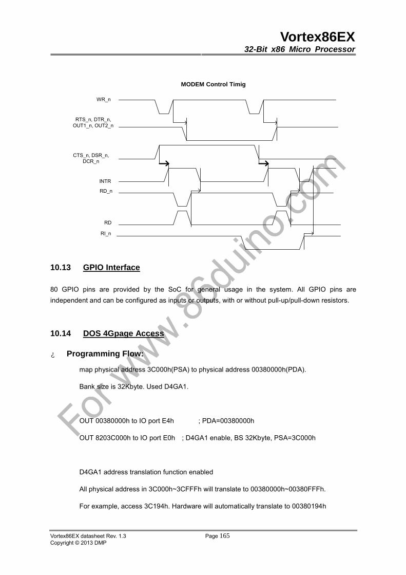
Vortex86EX32-Bit x86 Micro Processor
Vortex86EX datasheet Rev. 1.3 Page 165Copyright © 2013 DMP
WR_n
RTS_n, DTR_n,OUT1_n, OUT2_n
CTS_n, DSR_n,DCR_n
INTR
RD_n
RD
RI_n
MODEM Control Timig
10.13 GPIO Interface
80 GPIO pins are provided by the SoC for general usage in the system. All GPIO pins are
independent and can be configured as inputs or outputs, with or without pull-up/pull-down resistors.
10.14 DOS 4Gpage Access
� Programming Flow:
map physical address 3C000h(PSA) to physical address 00380000h(PDA).
Bank size is 32Kbyte. Used D4GA1.
OUT 00380000h to IO port E4h ; PDA=00380000h
OUT 8203C000h to IO port E0h ; D4GA1 enable, BS 32Kbyte, PSA=3C000h
D4GA1 address translation function enabled
All physical address in 3C000h~3CFFFh will translate to 00380000h~00380FFFh.
For example, access 3C194h. Hardware will automatically translate to 00380194h
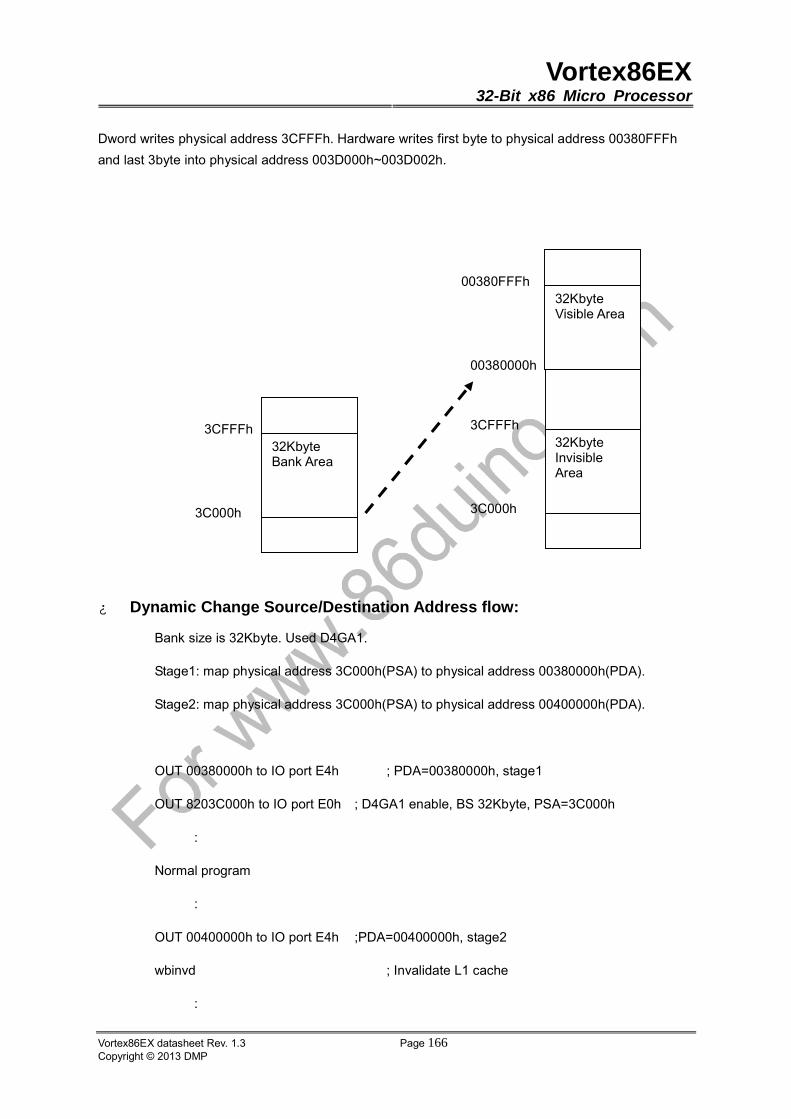
Vortex86EX32-Bit x86 Micro Processor
Vortex86EX datasheet Rev. 1.3 Page 166Copyright © 2013 DMP
Dword writes physical address 3CFFFh. Hardware writes first byte to physical address 00380FFFh
and last 3byte into physical address 003D000h~003D002h.
� Dynamic Change Source/Destination Address flow:
Bank size is 32Kbyte. Used D4GA1.
Stage1: map physical address 3C000h(PSA) to physical address 00380000h(PDA).
Stage2: map physical address 3C000h(PSA) to physical address 00400000h(PDA).
OUT 00380000h to IO port E4h ; PDA=00380000h, stage1
OUT 8203C000h to IO port E0h ; D4GA1 enable, BS 32Kbyte, PSA=3C000h
:
Normal program
:
OUT 00400000h to IO port E4h ;PDA=00400000h, stage2
wbinvd ; Invalidate L1 cache
:
32Kbyte Invisible Area
00380FFFh
32Kbyte Bank Area
3C000h
3CFFFh
32Kbyte Visible Area
00380000h
3C000h
3CFFFh
Vortex86EX32-Bit x86 Micro Processor
Vortex86EX datasheet Rev. 1.3 Page 167Copyright © 2013 DMP
Normal program
10.15 Flash Strap
In Vortex86EX, some functions and system configurateion are straped by specified address location
data value (flash region). We call this behavior “Flash Strap”. In system reset (even hardware reset or
software reset), Vortex86EX will re-do Flash Strap.
10.15.1 Flash Strap Region Summary.
Flash Address Location Flash Strap Function
(FFF)FFD00h - (FFF)FFDEFh CrossBar Config
(FFF)FFFB0h – (FFF)FFFB5h Ethernet MAC Address
(FFF)FFFB6h –(FFF)FFFB7h,
(FFF)FFFBBh –(FFF)FFFBFh PLL Config for Clock Frequency & Others Function Strap.
(FFF)FFFC0h –(FFF)FFFDFh Customer Data
10.15.2 CrossBar Config
� “CrossBar Flash Strap Header” must be 9A5BC341h, otherwise it’s recongnized as format error.
When CrossBar format error, CrossBar config will be reset to default value.
� “CrossBar Flash Strap Checksum” is calculated by below algorithm. If CrossBar checksum error,
CrossBar config will be reset to default value.
� (FFF)FFD10h –(FFF)FFDEFh: These config format are the same as “CrossBar Config
Registers” (check Chap.11.3.26).
Flash Address Location CrossBar Config Flash Strap
(FFF)FFD00h –(FFF)FFD03h CrossBar Flash Strap Header = “9A5BC341h”
FFF)FFD04h –(FFF)FFD07h CrossBar Flash Strap Checksum
(FFF)FFD10h –(FFF)FFD19h RichIO Port 0, 1, 2, …, 9 Selection
(FFF)FFD20h –(FFF)FFD27h Bit-RichIO Port0 Select
(FFF)FFD28h –(FFF)FFD2Fh Bit-RichIO Port1 Select
(FFF)FFD30h –(FFF)FFD37h Bit-RichIO Port2 Select
(FFF)FFD38h –(FFF)FFD3Bh On-Chip Device Power-Down Control 0
(FFF)FFD3Ch –(FFF)FFD3Fh On-Chip Device Power-Down Control 1
(FFF)FFD40h –(FFF)FFD8Fh CrossBar PAD Attribute
(FFF)FFD90h –(FFF)FFD99h CrossBar-Port Group Selection, Port0, Port1, …, Port9
(FFF)FFDA0h - (FFF)FFDEFh CrossBar-Bit Group Selection, Bit 0,1,2, …, 79
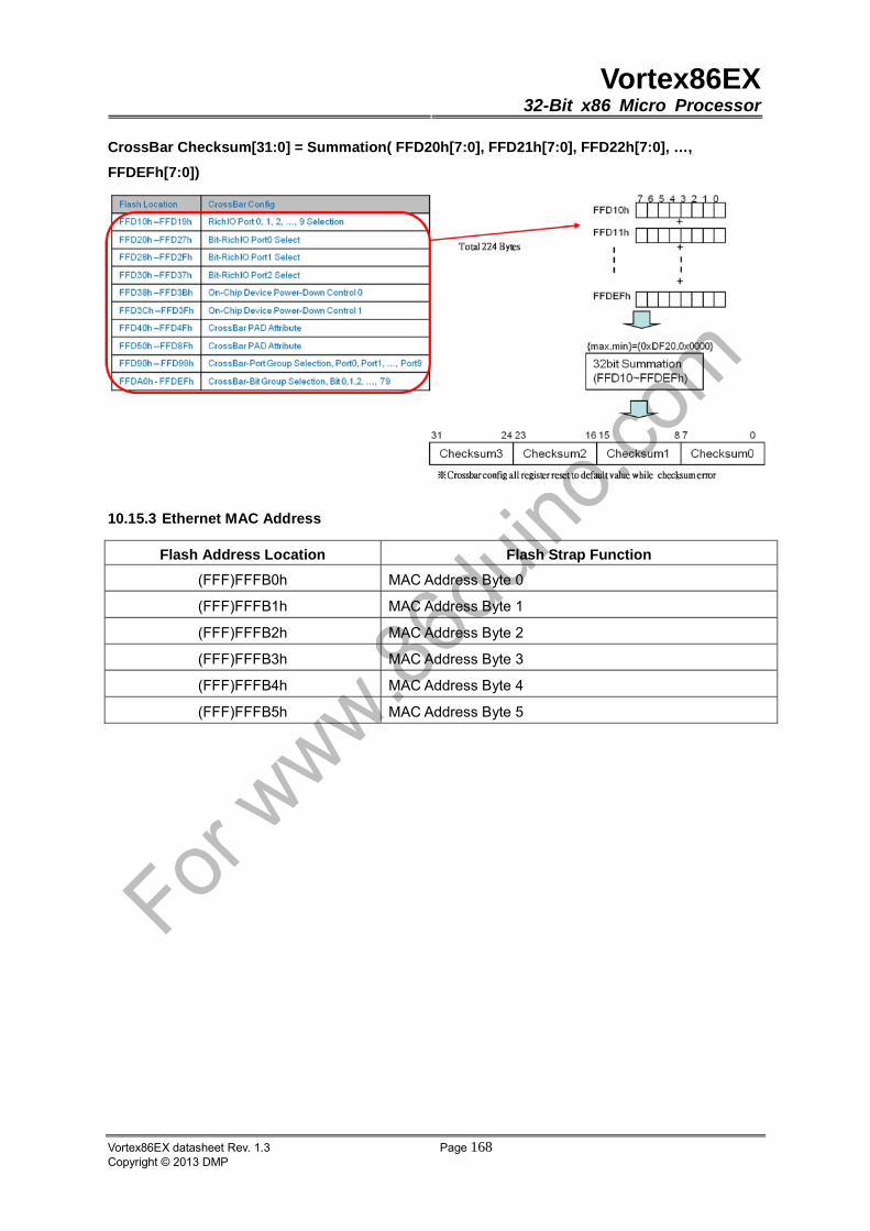
Vortex86EX32-Bit x86 Micro Processor
Vortex86EX datasheet Rev. 1.3 Page 168Copyright © 2013 DMP
CrossBar Checksum[31:0] = Summation( FFD20h[7:0], FFD21h[7:0], FFD22h[7:0], …,
FFDEFh[7:0])
10.15.3 Ethernet MAC Address
Flash Address Location Flash Strap Function
(FFF)FFFB0h MAC Address Byte 0
(FFF)FFFB1h MAC Address Byte 1
(FFF)FFFB2h MAC Address Byte 2
(FFF)FFFB3h MAC Address Byte 3
(FFF)FFFB4h MAC Address Byte 4
(FFF)FFFB5h MAC Address Byte 5

Vortex86EX32-Bit x86 Micro Processor
Vortex86EX datasheet Rev. 1.3 Page 169Copyright © 2013 DMP
10.15.4 PLL Config & Others
� “PLL Flash Strap Checksum” is calculated by below algorithm. If PLL checksum error, PLL
config will be reset to default value.
TMP_SUM[9:0] = Summation( FFFB6h[7:0], FFFB7h[7:0], FFFBBh[7:0], FFFBCh[7:0])
PLL Checksum[3:0] = Summation( TMP_SUM[9:8], TMP_SUM[7:4], TMP_SUM[3:0])
Flash Address Location Flash Strap Function
(FFF)FFFB6h CPU_NS
(FFF)FFFB7h
Bits[1:0] = CPU_MS
Bits[3:2] = CPU_RS
Bits[5:4] = CPU_DIV
Bits[6] = DRAM_DIV
(FFF)FFFBBh
Bits[3:0] = PCI_DIV
Bits[5:4] = PCI_Mode
Bits[6] = PLL1M
Bits[7] = PLL2M
(FFF)FFFBCh
Bits[2:0] = PLL1_IPSEL
Bit[3] = DIS_D3WL
Bit[4] = DIS_D3GT
Bit[5] = DIS_SPIbp
(FFF)FFFBDh Bits[7:4] = Checksum
(FFF)FFFBEh BOARD ID(L)
(FFF)FFFBFh Bits[3:0] = BOARD ID(H)
10.15.5 Customer Data
� These regions are encoded data for Customer usage. After system reset, these data are
decoded to NB function0 Config Registers.
Flash Address Location Flash Strap Function
(FFF)FFFC0h - (FFF)FFFDFh Decode to NB Function0 Config Reg D0h – Efh
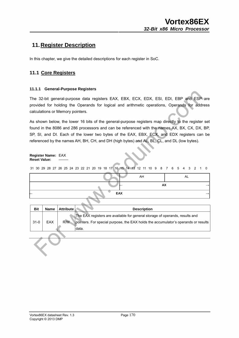
Vortex86EX32-Bit x86 Micro Processor
Vortex86EX datasheet Rev. 1.3 Page 170Copyright © 2013 DMP
11. Register Description
In this chapter, we give the detailed descriptions for each register in SoC.
11.1 Core Registers
11.1.1 General-Purpose Registers
The 32-bit general-purpose data registers EAX, EBX, ECX, EDX, ESI, EDI, EBP and ESP are
provided for holding the Operands for logical and arithmetic operations, Operands for address
calculations or Memory pointers.
As shown below, the lower 16 bits of the general-purpose registers map directly to the register set
found in the 8086 and 286 processors and can be referenced with the names AX, BX, CX, DX, BP,
SP, SI, and DI. Each of the lower two bytes of the EAX, EBX, ECX, and EDX registers can be
referenced by the names AH, BH, CH, and DH (high bytes) and AL, BL, CL, and DL (low bytes).
Register Name: EAX Reset Value: --------
31 30 29 28 27 26 25 24 23 22 21 20 19 18 17 16 15 14 13 12 11 10 9 8 7 6 5 4 3 2 1 0
AH AL
← AX →
← EAX →
Bit Name Attribute Description
31-0 EAX R/W
The EAX registers are available for general storage of operands, results and
pointers. For special purpose, the EAX holds the accumulator’s operands or results
data.

Vortex86EX32-Bit x86 Micro Processor
Vortex86EX datasheet Rev. 1.3 Page 171Copyright © 2013 DMP
Register Name: EBX Reset Value: --------
31 30 29 28 27 26 25 24 23 22 21 20 19 18 17 16 15 14 13 12 11 10 9 8 7 6 5 4 3 2 1 0
BH BL
← BX →
← EBX →
Bit Name Attribute Description
31-0 EBX R/W
The EBX registers are available for general storage of operands, results and
pointers. For special purpose, the EBX holds a pointer which points to data in the
DS segment.
Register Name: ECX Reset Value: --------
31 30 29 28 27 26 25 24 23 22 21 20 19 18 17 16 15 14 13 12 11 10 9 8 7 6 5 4 3 2 1 0
CH CL
← CX →
← ECX →
Bit Name Attribute Description
31-0 ECX R/W
The ECX registers are available for general storage of operands, results and
pointers. For special purpose, the ECX holds a string pointer or the counter values
of loop operations.
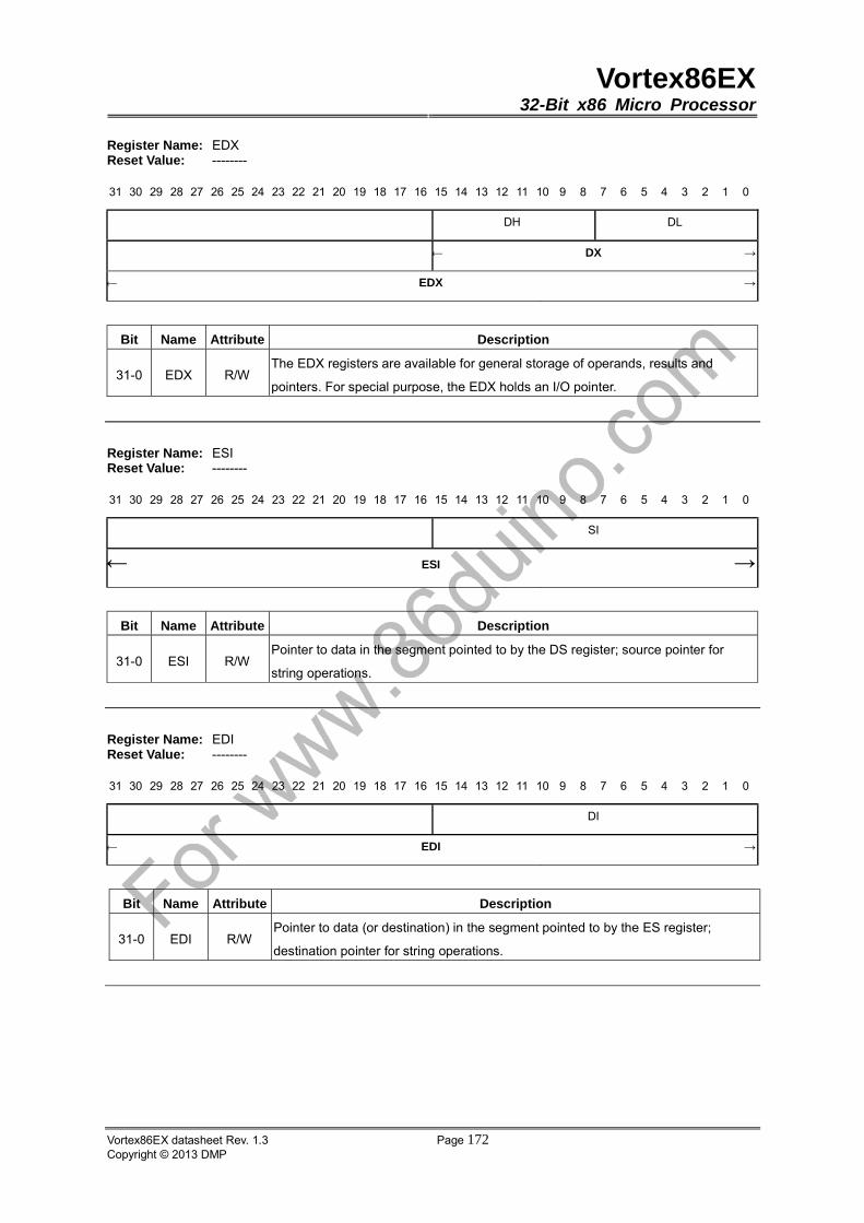
Vortex86EX32-Bit x86 Micro Processor
Vortex86EX datasheet Rev. 1.3 Page 172Copyright © 2013 DMP
Register Name: EDX Reset Value: --------
31 30 29 28 27 26 25 24 23 22 21 20 19 18 17 16 15 14 13 12 11 10 9 8 7 6 5 4 3 2 1 0
DH DL
← DX →
← EDX →
Bit Name Attribute Description
31-0 EDX R/W The EDX registers are available for general storage of operands, results and
pointers. For special purpose, the EDX holds an I/O pointer.
Register Name: ESI Reset Value: --------
31 30 29 28 27 26 25 24 23 22 21 20 19 18 17 16 15 14 13 12 11 10 9 8 7 6 5 4 3 2 1 0
SI
← ESI →
Bit Name Attribute Description
31-0 ESI R/W Pointer to data in the segment pointed to by the DS register; source pointer for
string operations.
Register Name: EDI Reset Value: --------
31 30 29 28 27 26 25 24 23 22 21 20 19 18 17 16 15 14 13 12 11 10 9 8 7 6 5 4 3 2 1 0
DI
← EDI →
Bit Name Attribute Description
31-0 EDI R/W Pointer to data (or destination) in the segment pointed to by the ES register;
destination pointer for string operations.
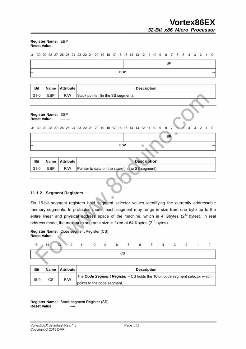
Vortex86EX32-Bit x86 Micro Processor
Vortex86EX datasheet Rev. 1.3 Page 173Copyright © 2013 DMP
Register Name: EBP Reset Value: --------
31 30 29 28 27 26 25 24 23 22 21 20 19 18 17 16 15 14 13 12 11 10 9 8 7 6 5 4 3 2 1 0
BP
← EBP →
Bit Name Attribute Description
31-0 EBP R/W Stack pointer (in the SS segment).
Register Name: ESP Reset Value: --------
31 30 29 28 27 26 25 24 23 22 21 20 19 18 17 16 15 14 13 12 11 10 9 8 7 6 5 4 3 2 1 0
BP
← ESP →
Bit Name Attribute Description
31-0 EBP R/W Pointer to data on the stack (in the SS segment).
11.1.2 Segment Registers
Six 16-bit segment registers hold segment selector values identifying the currently addressable
memory segments. In protected mode, each segment may range in size from one byte up to the
entire linear and physical address space of the machine, which is 4 Gbytes (232 bytes). In real
address mode, the maximum segment size is fixed at 64 Kbytes (216 bytes).
Register Name: Code segment Register (CS) Reset Value: ----
15 14 13 12 11 10 9 8 7 6 5 4 3 2 1 0
CS
Bit Name Attribute Description
15-0 CS R/W The Code Segment Register – CS holds the 16-bit code segment selector which
points to the code segment.
Register Name: Stack segment Register (SS) Reset Value: ----

Vortex86EX32-Bit x86 Micro Processor
Vortex86EX datasheet Rev. 1.3 Page 174Copyright © 2013 DMP
15 14 13 12 11 10 9 8 7 6 5 4 3 2 1 0
SS
Bit Name Attribute Description
15-0 SS R/W The Stack Segment Register –SS holds the 16-bit stack segment selector.
Register Name: Data segment Register (DS) Reset Value: ----
15 14 13 12 11 10 9 8 7 6 5 4 3 2 1 0
DS
Bit Name Attribute Description
15-0 DS R/W The Data Segment Register – DS holds the data segment selector.
Register Name: Data segment Register (ES) Reset Value: ----
15 14 13 12 11 10 9 8 7 6 5 4 3 2 1 0
ES
Bit Name Attribute Description
15-0 ES R/W The Data Segment Register – ES holds the data segment selector.
Register Name: Data segment Register (FS) Reset Value: ----
15 14 13 12 11 10 9 8 7 6 5 4 3 2 1 0
FS
Bit Name Attribute Description
15-0 FS R/W The Data Segment Register – FS holds the data segment selector.
Register Name: Data segment Register (GS) Reset Value: ----
15 14 13 12 11 10 9 8 7 6 5 4 3 2 1 0
GS
Vortex86EX32-Bit x86 Micro Processor
Vortex86EX datasheet Rev. 1.3 Page 175Copyright © 2013 DMP
Bit Name Attribute Description
15-0 GS R/W The Data Segment Register – GS holds the data segment selector.
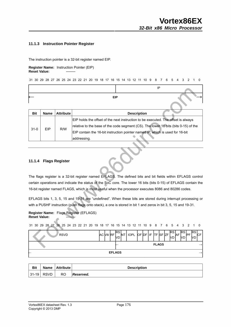
Vortex86EX32-Bit x86 Micro Processor
Vortex86EX datasheet Rev. 1.3 Page 176Copyright © 2013 DMP
11.1.3 Instruction Pointer Register
The instruction pointer is a 32-bit register named EIP.
Register Name: Instruction Pointer (EIP) Reset Value: --------
31 30 29 28 27 26 25 24 23 22 21 20 19 18 17 16 15 14 13 12 11 10 9 8 7 6 5 4 3 2 1 0
IP
← EIP →
Bit Name Attribute Description
31-0 EIP R/W
EIP holds the offset of the next instruction to be executed. The offset is always
relative to the base of the code segment (CS). The lower 16 bits (bits 0-15) of the
EIP contain the 16-bit instruction pointer named IP, which is used for 16-bit
addressing.
11.1.4 Flags Register
The flags register is a 32-bit register named EFLAGS. The defined bits and bit fields within EFLAGS control
certain operations and indicate the status of the SoC core. The lower 16 bits (bits 0-15) of EFLAGS contain the
16-bit register named FLAGS, which is most useful when the processor executes 8086 and 80286 codes.
EFLAGS bits 1, 3, 5, 15 and 19-31 are “undefined”. When these bits are stored during interrupt processing or
with a PUSHF instruction (push flags onto stack), a one is stored in bit 1 and zeros in bit 3, 5, 15 and 19-31.
Register Name: Flags Register (EFLAGS) Reset Value: --------
31 30 29 28 27 26 25 24 23 22 21 20 19 18 17 16 15 14 13 12 11 10 9 8 7 6 5 4 3 2 1 0
RSVD AC VM RFRS
VDNT IOPL OF DF IF TF SF ZF
RS
VDAF
RS
VDPF
RS
VDCF
← FLAGS →
← EFLAGS →
Bit Name Attribute Description
31-19 RSVD RO Reserved.
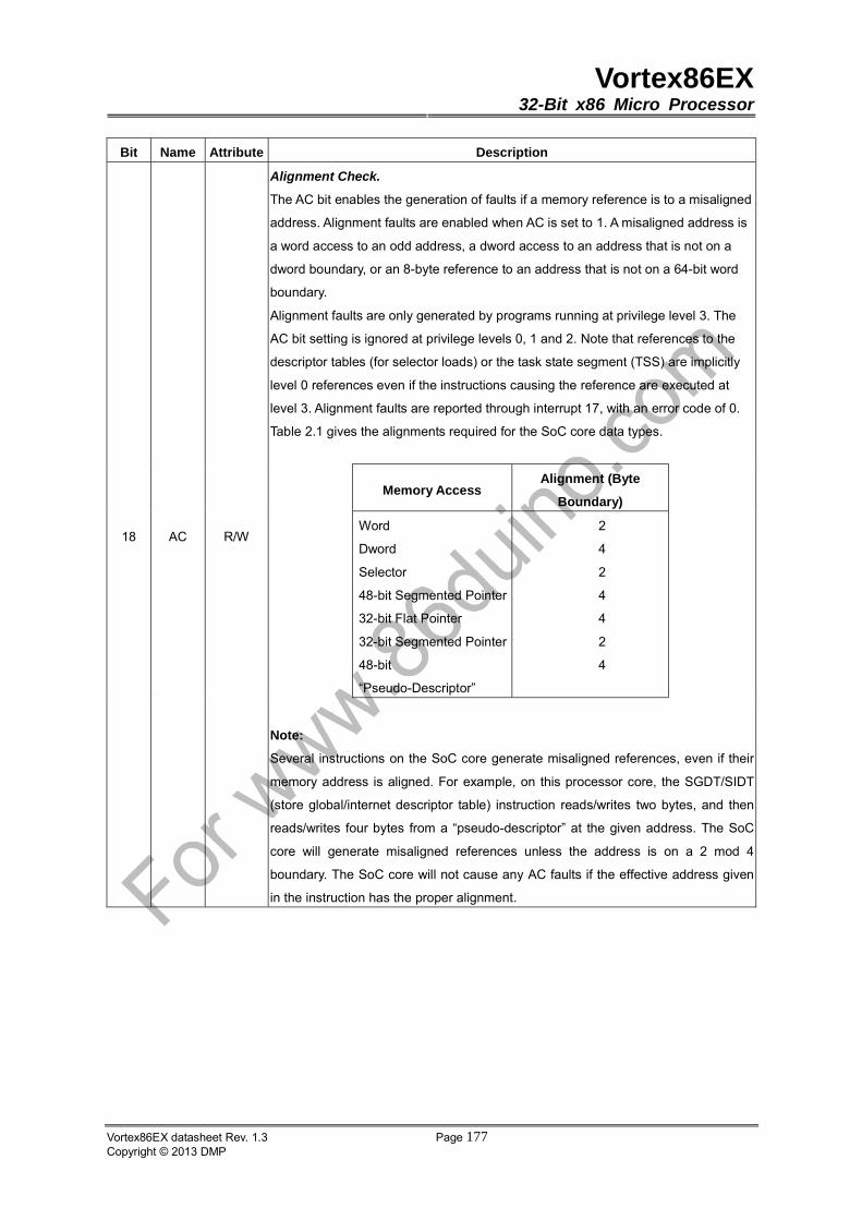
Vortex86EX32-Bit x86 Micro Processor
Vortex86EX datasheet Rev. 1.3 Page 177Copyright © 2013 DMP
Bit Name Attribute Description
Alignment Check.
The AC bit enables the generation of faults if a memory reference is to a misaligned
address. Alignment faults are enabled when AC is set to 1. A misaligned address is
a word access to an odd address, a dword access to an address that is not on a
dword boundary, or an 8-byte reference to an address that is not on a 64-bit word
boundary.
Alignment faults are only generated by programs running at privilege level 3. The
AC bit setting is ignored at privilege levels 0, 1 and 2. Note that references to the
descriptor tables (for selector loads) or the task state segment (TSS) are implicitly
level 0 references even if the instructions causing the reference are executed at
level 3. Alignment faults are reported through interrupt 17, with an error code of 0.
Table 2.1 gives the alignments required for the SoC core data types.
Memory Access Alignment (Byte
Boundary)
Word
Dword
Selector
48-bit Segmented Pointer
32-bit Flat Pointer
32-bit Segmented Pointer
48-bit
“Pseudo-Descriptor”
2
4
2
4
4
2
4
18 AC R/W
Note:
Several instructions on the SoC core generate misaligned references, even if their
memory address is aligned. For example, on this processor core, the SGDT/SIDT
(store global/internet descriptor table) instruction reads/writes two bytes, and then
reads/writes four bytes from a “pseudo-descriptor” at the given address. The SoC
core will generate misaligned references unless the address is on a 2 mod 4
boundary. The SoC core will not cause any AC faults if the effective address given
in the instruction has the proper alignment.

Vortex86EX32-Bit x86 Micro Processor
Vortex86EX datasheet Rev. 1.3 Page 178Copyright © 2013 DMP
Bit Name Attribute Description
17 VM R/W
Virtual 8086 Mode.
The VM bit provides virtual 8086 mode within protected mode. If set while the SoC
core is in protected mode, the processor core will switch to virtual 8086 operation,
handling segment loads as the 8086 does, but generating exception 13 faults on
privileged opcodes. The VM bit can be set only in protected mode, by the IRET
instruction (if the current privilege level = 0) and by task switches at any privilege
level. The VM bit is unaffected by POPF. PUSHF always pushes a 0 in this bit, even
if executing in virtual 8086 mode. The EFLAGS image pushed during interrupt
processing or saved during task switches will contain a 1 in this bit if the interrupted
code was executing as a virtual 8086 task.
16 RF R/W
Resume Flag.
The RF flag is used in conjunction with the debug register breakpoints. It is checked
at instruction boundaries before breakpoint processing. When RF is set, it causes
any debug fault to be ignored on the next instruction. RF is then automatically reset
at the successful completion of every instruction (no faults are signaled) except the
IRET instruction, the POPF instruction, and JMP, CALL, and INT instructions
causing a task switch. These instructions set RF to the value specified by the
memory image. For example, at the end of the breakpoint service routine, the IRET
instruction can pop an EFLAG image having the RF bit set and resume the
program’s execution at the breakpoint address without generating another
breakpoint fault on the same location.
15 RSVD RO Reserved.
14 NT R/W
Nested Task.
This flag applies to Protected Mode. NT is set to indicate that the execution of this
task is nested within another task. If set, it indicates that the current nested task’s
Task State Segment (TSS) has a valid back link to the previous task’s TSS. This bit
is set or reset by control transfers to other tasks. The value of NT in EFLAGS is
tested by the IRET instruction to determine whether to do an inter-task return or an
intra-task return. A POPF or an IRET instruction will affect the setting of this bit
according to the image popped, at any privilege level.
13-12 IOPL R/W
Input/Output Privilege Level.
This two-bit field applies to Protected Mode. IOPL indicates the numerically
maximum CPL (current privilege level) value permitted to execute I/O instructions
without generating an exception 13 faults or consulting the I/O Permission Bitmap.
It also indicates the maximum CPL value allowing alteration of the IF (INTR Enable
Flag) bit when new values are popped into the EFLAG register. POPF and IRET
instructions can alter the IOPL field when executed at CPL = 0. Task switches can
always alter the IOPL field when the new flag image is loaded from the incoming
task’s TSS.

Vortex86EX32-Bit x86 Micro Processor
Vortex86EX datasheet Rev. 1.3 Page 179Copyright © 2013 DMP
Bit Name Attribute Description
11 OF R/W
Overflow Flag.
OF is set if the operation resulted in signed overflow. Signed overflow occurs when
the operation resulted in carry/borrow into the sign bit (high-order bit) of the result
but did not result in a carry/borrow out of the high-order bit, or vice-versa. For 8-,
16- and 32-bit operations, OF is set according to overflow at bit 7, 15 and 31
respectively.
10 DF R/W
Direction Flag.
DF defines whether ESI and/or EDI register postdecrement or postincrement during
the string instructions. Postinstruction occurs if DF is reset. Post decrement occurs
if DF is set.
9 IF R/W
INTR Enable Flag.
The IF flag, when set, allows recognition of external interrupts signaled on the INTR
pin. When IF is reset, external interrupts signaled on the INTR are not recognized.
IOPL indicates the maximum CPL value allowing alteration of the IF bit when new
values are popped into EFLAGS or FLAGS.
8 TF R/W
Trap Enable Flag.
TF controls the generation of exception 1 trap when single-stepping through code.
When TF is set, the SoC core generates an exception 1 trap after the next
instruction is executed. When TF is reset, exception 1 traps occur only as a function
of the breakpoint addresses loaded into debug registers DR[0:3].
7 SF R/W
Sign Flag.
SF is set if the high-order bit of the result is set, it is reset otherwise. For 8-, 16- and
32-bit operations, SF reflects the state of bit 7, 15 and 31 respectively.
6 ZF R/W Zero Flag.
ZF is set if all bits of the result are 0. Otherwise it is reset.
5 RSVD RO Reserved.
4 AF R/W
Auxiliary Carry Flag.
The Auxiliary Flag is used to simplify the addition and subtraction of packed BCD
quantities. AF is set if the operation results in a carry out of bit 3 (addition) or a
borrow into bit 3 (subtraction). Otherwise AF is reset. AF is affected by carry out of,
or borrow into bit 3 only, regardless of overall operand length: 8, 16 or 32 bits.
3 RSVD RO Reserved.
2 PF R/W
Parity Flags.
PF is set if the low-order eight bits of the operation contain an even number of “1”s
(even parity). PF is reset if the low-order eight bits have odd parity. PF is a function
of only the low-order eight bits, regardless of operand size.
1 RSVD RO Reserved.
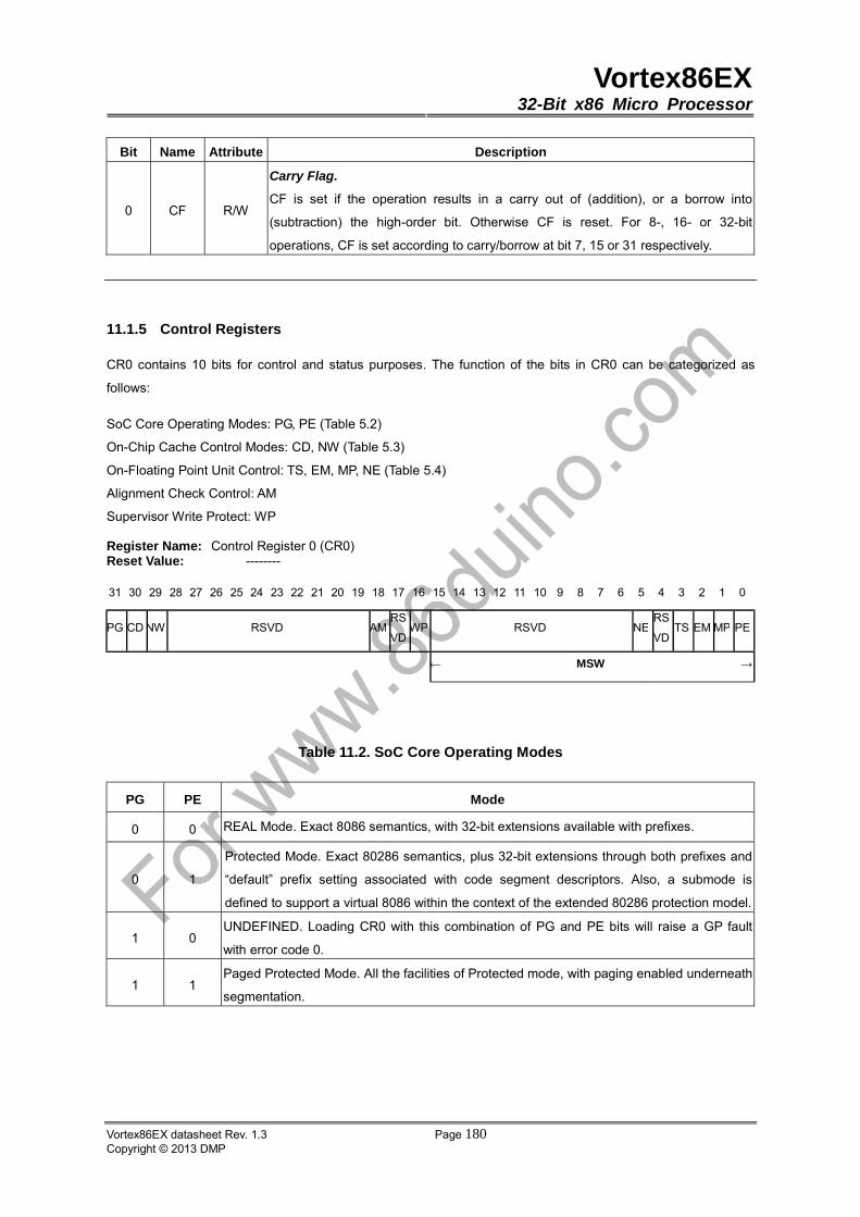
Vortex86EX32-Bit x86 Micro Processor
Vortex86EX datasheet Rev. 1.3 Page 180Copyright © 2013 DMP
Bit Name Attribute Description
0 CF R/W
Carry Flag.
CF is set if the operation results in a carry out of (addition), or a borrow into
(subtraction) the high-order bit. Otherwise CF is reset. For 8-, 16- or 32-bit
operations, CF is set according to carry/borrow at bit 7, 15 or 31 respectively.
11.1.5 Control Registers
CR0 contains 10 bits for control and status purposes. The function of the bits in CR0 can be categorized as
follows:
SoC Core Operating Modes: PG, PE (Table 5.2)
On-Chip Cache Control Modes: CD, NW (Table 5.3)
On-Floating Point Unit Control: TS, EM, MP, NE (Table 5.4)
Alignment Check Control: AM
Supervisor Write Protect: WP
Register Name: Control Register 0 (CR0) Reset Value: --------
31 30 29 28 27 26 25 24 23 22 21 20 19 18 17 16 15 14 13 12 11 10 9 8 7 6 5 4 3 2 1 0
PG CD NW RSVD AMRS
VDWP RSVD NE
RS
VDTS EM MP PE
← MSW →
Table 11.2. SoC Core Operating Modes
PG PE Mode
0 0 REAL Mode. Exact 8086 semantics, with 32-bit extensions available with prefixes.
0 1
Protected Mode. Exact 80286 semantics, plus 32-bit extensions through both prefixes and
“default” prefix setting associated with code segment descriptors. Also, a submode is
defined to support a virtual 8086 within the context of the extended 80286 protection model.
1 0 UNDEFINED. Loading CR0 with this combination of PG and PE bits will raise a GP fault
with error code 0.
1 1 Paged Protected Mode. All the facilities of Protected mode, with paging enabled underneath
segmentation.
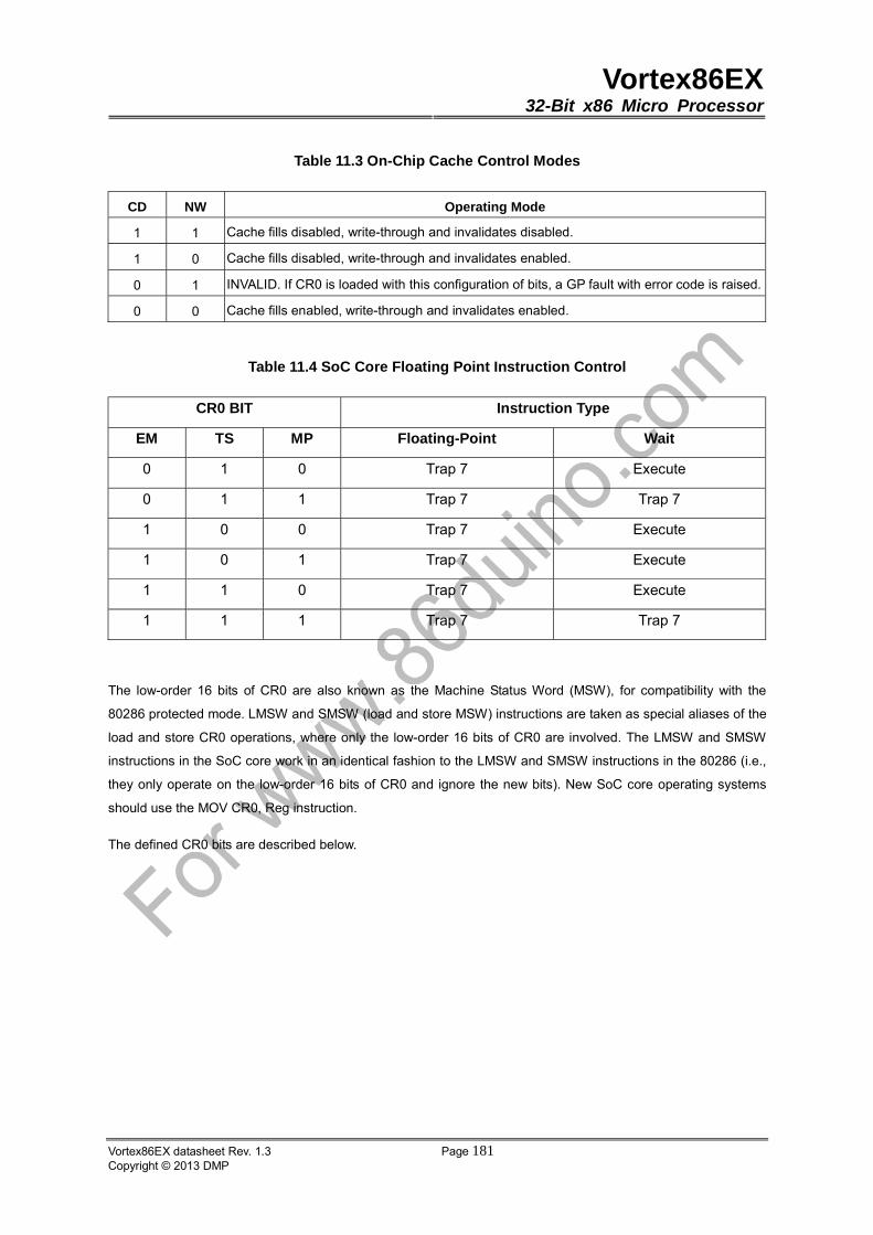
Vortex86EX32-Bit x86 Micro Processor
Vortex86EX datasheet Rev. 1.3 Page 181Copyright © 2013 DMP
Table 11.3 On-Chip Cache Control Modes
CD NW Operating Mode
1 1 Cache fills disabled, write-through and invalidates disabled.
1 0 Cache fills disabled, write-through and invalidates enabled.
0 1 INVALID. If CR0 is loaded with this configuration of bits, a GP fault with error code is raised.
0 0 Cache fills enabled, write-through and invalidates enabled.
Table 11.4 SoC Core Floating Point Instruction Control
CR0 BIT Instruction Type
EM TS MP Floating-Point Wait
0 1 0 Trap 7 Execute
0 1 1 Trap 7 Trap 7
1 0 0 Trap 7 Execute
1 0 1 Trap 7 Execute
1 1 0 Trap 7 Execute
1 1 1 Trap 7 Trap 7
The low-order 16 bits of CR0 are also known as the Machine Status Word (MSW), for compatibility with the
80286 protected mode. LMSW and SMSW (load and store MSW) instructions are taken as special aliases of the
load and store CR0 operations, where only the low-order 16 bits of CR0 are involved. The LMSW and SMSW
instructions in the SoC core work in an identical fashion to the LMSW and SMSW instructions in the 80286 (i.e.,
they only operate on the low-order 16 bits of CR0 and ignore the new bits). New SoC core operating systems
should use the MOV CR0, Reg instruction.
The defined CR0 bits are described below.
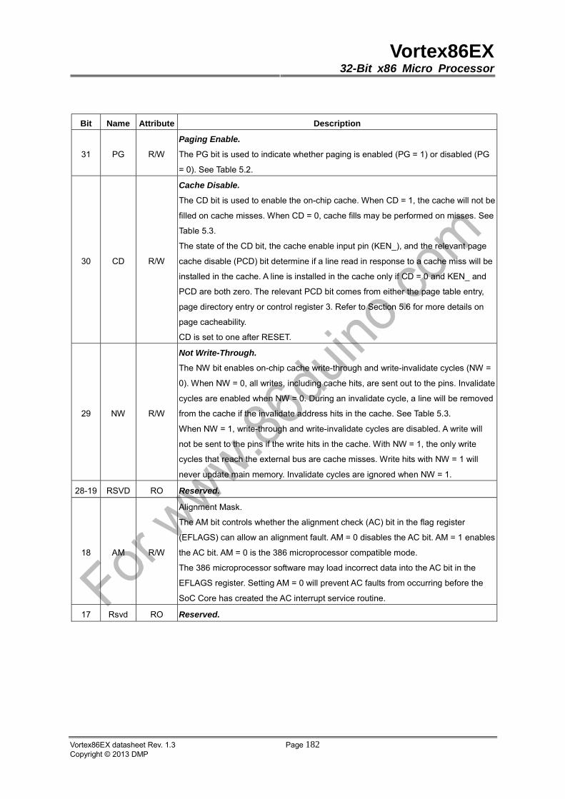
Vortex86EX32-Bit x86 Micro Processor
Vortex86EX datasheet Rev. 1.3 Page 182Copyright © 2013 DMP
Bit Name Attribute Description
31 PG R/W
Paging Enable.
The PG bit is used to indicate whether paging is enabled (PG = 1) or disabled (PG
= 0). See Table 5.2.
30 CD R/W
Cache Disable.
The CD bit is used to enable the on-chip cache. When CD = 1, the cache will not be
filled on cache misses. When CD = 0, cache fills may be performed on misses. See
Table 5.3.
The state of the CD bit, the cache enable input pin (KEN_), and the relevant page
cache disable (PCD) bit determine if a line read in response to a cache miss will be
installed in the cache. A line is installed in the cache only if CD = 0 and KEN_ and
PCD are both zero. The relevant PCD bit comes from either the page table entry,
page directory entry or control register 3. Refer to Section 5.6 for more details on
page cacheability.
CD is set to one after RESET.
29 NW R/W
Not Write-Through.
The NW bit enables on-chip cache write-through and write-invalidate cycles (NW =
0). When NW = 0, all writes, including cache hits, are sent out to the pins. Invalidate
cycles are enabled when NW = 0. During an invalidate cycle, a line will be removed
from the cache if the invalidate address hits in the cache. See Table 5.3.
When NW = 1, write-through and write-invalidate cycles are disabled. A write will
not be sent to the pins if the write hits in the cache. With NW = 1, the only write
cycles that reach the external bus are cache misses. Write hits with NW = 1 will
never update main memory. Invalidate cycles are ignored when NW = 1.
28-19 RSVD RO Reserved.
18 AM R/W
Alignment Mask.
The AM bit controls whether the alignment check (AC) bit in the flag register
(EFLAGS) can allow an alignment fault. AM = 0 disables the AC bit. AM = 1 enables
the AC bit. AM = 0 is the 386 microprocessor compatible mode.
The 386 microprocessor software may load incorrect data into the AC bit in the
EFLAGS register. Setting AM = 0 will prevent AC faults from occurring before the
SoC Core has created the AC interrupt service routine.
17 Rsvd RO Reserved.

Vortex86EX32-Bit x86 Micro Processor
Vortex86EX datasheet Rev. 1.3 Page 183Copyright © 2013 DMP
Bit Name Attribute Description
16 WP R/W
Write Protect.
WP protects read-only pages from supervisor write access. The 386
microprocessor allows a read-only page to be written from privilege level 0-2. The
SoC Core is compatible with the 386 microprocessor when WP = 0. WP = 1 forces
a fault on a write to a read-only page from any privilege level. Operating systems
with Copy-on-Write features can be supported with the WP bit. Refer to Section
5.5.3 for further details on use of the WP bit.
15-6 RSVD RO Reserved.
5 NE R/W
Numerics Exception.
For the SoC Core, interrupt 7 will be generated upon encountering any
floating-point instruction regardless of the value of the NE bit. It is recommended
that NE = 1 for normal operation of the SoC Core.
4 RSVD RO Reserved.
3 TS R/W
Task Switch.
The TS bit is set whenever a task switch operation is performed. Execution of
floating point instructions with TS = 1 will cause a “device not available” (DNA) fault
(trap vector 7). With MP = 0, the value of the TS bit is a “don’t care” for the WAIT
instructions, i.e., these instructions will not generate trap 7.
2 EM R/W
Emulate Coprocessor.
The EM bit should be set to one for the SoC Core. This will cause the processor
core to trap via interrupt vector 7 (Device Not Available) to a software exception
handler whenever it encounters a floating-point instruction. If EM bit is 0, the
system will hang.
1 MP R/W
Monitor Coprocessor.
For normal operation of the SoC Core, it is required to set this bit as zero (MP = 0).
The MP bit is used in conjunction with the TS bit to determine if WAIT instructions
should trap. For MP = 0, the value of TS is a “don’t care” for these type of
instructions.
0 PE R/W
Protection Enable.
The PE bit enables the segment based protection mechanism. If PE = 1, protection
is enabled. When PE = 0, the SoC Core operates in REAL mode, with segment
based protection disabled, and addresses formed as in an 8086. Refer to Table 5.2.
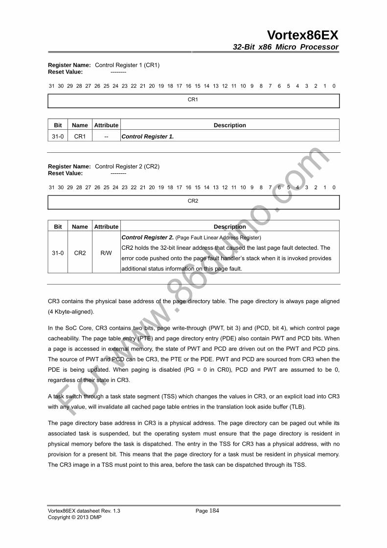
Vortex86EX32-Bit x86 Micro Processor
Vortex86EX datasheet Rev. 1.3 Page 184Copyright © 2013 DMP
Register Name: Control Register 1 (CR1) Reset Value: --------
31 30 29 28 27 26 25 24 23 22 21 20 19 18 17 16 15 14 13 12 11 10 9 8 7 6 5 4 3 2 1 0
CR1
Bit Name Attribute Description
31-0 CR1 -- Control Register 1.
Register Name: Control Register 2 (CR2) Reset Value: --------
31 30 29 28 27 26 25 24 23 22 21 20 19 18 17 16 15 14 13 12 11 10 9 8 7 6 5 4 3 2 1 0
CR2
Bit Name Attribute Description
31-0 CR2 R/W
Control Register 2. (Page Fault Linear Address Register)
CR2 holds the 32-bit linear address that caused the last page fault detected. The
error code pushed onto the page fault handler’s stack when it is invoked provides
additional status information on this page fault.
CR3 contains the physical base address of the page directory table. The page directory is always page aligned
(4 Kbyte-aligned).
In the SoC Core, CR3 contains two bits, page write-through (PWT, bit 3) and (PCD, bit 4), which control page
cacheability. The page table entry (PTE) and page directory entry (PDE) also contain PWT and PCD bits. When
a page is accessed in external memory, the state of PWT and PCD are driven out on the PWT and PCD pins.
The source of PWT and PCD can be CR3, the PTE or the PDE. PWT and PCD are sourced from CR3 when the
PDE is being updated. When paging is disabled (PG = 0 in CR0), PCD and PWT are assumed to be 0,
regardless of their state in CR3.
A task switch through a task state segment (TSS) which changes the values in CR3, or an explicit load into CR3
with any value, will invalidate all cached page table entries in the translation look aside buffer (TLB).
The page directory base address in CR3 is a physical address. The page directory can be paged out while its
associated task is suspended, but the operating system must ensure that the page directory is resident in
physical memory before the task is dispatched. The entry in the TSS for CR3 has a physical address, with no
provision for a present bit. This means that the page directory for a task must be resident in physical memory.
The CR3 image in a TSS must point to this area, before the task can be dispatched through its TSS.
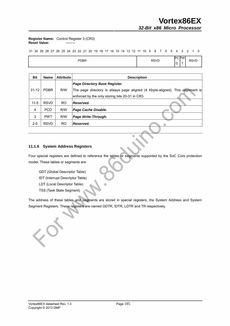
Vortex86EX32-Bit x86 Micro Processor
Vortex86EX datasheet Rev. 1.3 Page 185Copyright © 2013 DMP
Register Name: Control Register 3 (CR3) Reset Value: --------
31 30 29 28 27 26 25 24 23 22 21 20 19 18 17 16 15 14 13 12 11 10 9 8 7 6 5 4 3 2 1 0
PDBR RSVD PC
D
PW
TRSVD
Bit Name Attribute Description
31-12 PDBR R/W
Page Directory Base Register.
The page directory is always page aligned (4 Kbyte-aligned). This alignment is
enforced by the only storing bits 20-31 in CR3.
11-5 RSVD RO Reserved.
4 PCD R/W Page Cache Disable.
3 PWT R/W Page Write-Through.
2-0 RSVD RO Reserved.
11.1.6 System Address Registers
Four special registers are defined to reference the tables or segments supported by the SoC Core protection
model. These tables or segments are:
GDT (Global Descriptor Table)
IDT (Interrupt Descriptor Table)
LDT (Local Descriptor Table)
TSS (Task State Segment)
The address of these tables and segments are stored in special registers, the System Address and System
Segment Registers. These registers are named GDTR, IDTR, LDTR and TR respectively.
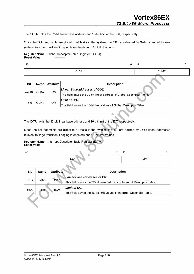
Vortex86EX32-Bit x86 Micro Processor
Vortex86EX datasheet Rev. 1.3 Page 186Copyright © 2013 DMP
The GDTR holds the 32-bit linear base address and 16-bit limit of the GDT, respectively.
Since the GDT segments are global to all tasks in the system, the GDT are defined by 32-bit linear addresses
(subject to page transition if paging is enabled) and 16-bit limit values.
Register Name: Global Descriptor Table Register (GDTR) Reset Value: ----------
47 16 15 0
GLBA GLIMT
Bit Name Attribute Description
47-16 GLBA R/W Linear Base addresses of GDT.
This field saves the 32-bit linear address of Global Descriptor Table.
15-0 GLMT R/W Limit of GDT.
This field saves the 16-bit limit values of Global Descriptor Table.
The IDTR holds the 32-bit linear base address and 16-bit limit of the IDT, respectively.
Since the IDT segments are global to all tasks in the system, the IDT are defined by 32-bit linear addresses
(subject to page transition if paging is enabled) and 16-bit limit values.
Register Name: Interrupt Descriptor Table Register (IDTR) Reset Value: ----------
47 16 15 0
ILBA ILIMT
Bit Name Attribute Description
47-16 ILBA R/W Linear Base addresses of IDT.
This field saves the 32-bit linear address of Interrupt Descriptor Table.
15-0 ILMT R/W Limit of IDT.
This field saves the 16-bit limit values of Interrupt Descriptor Table.
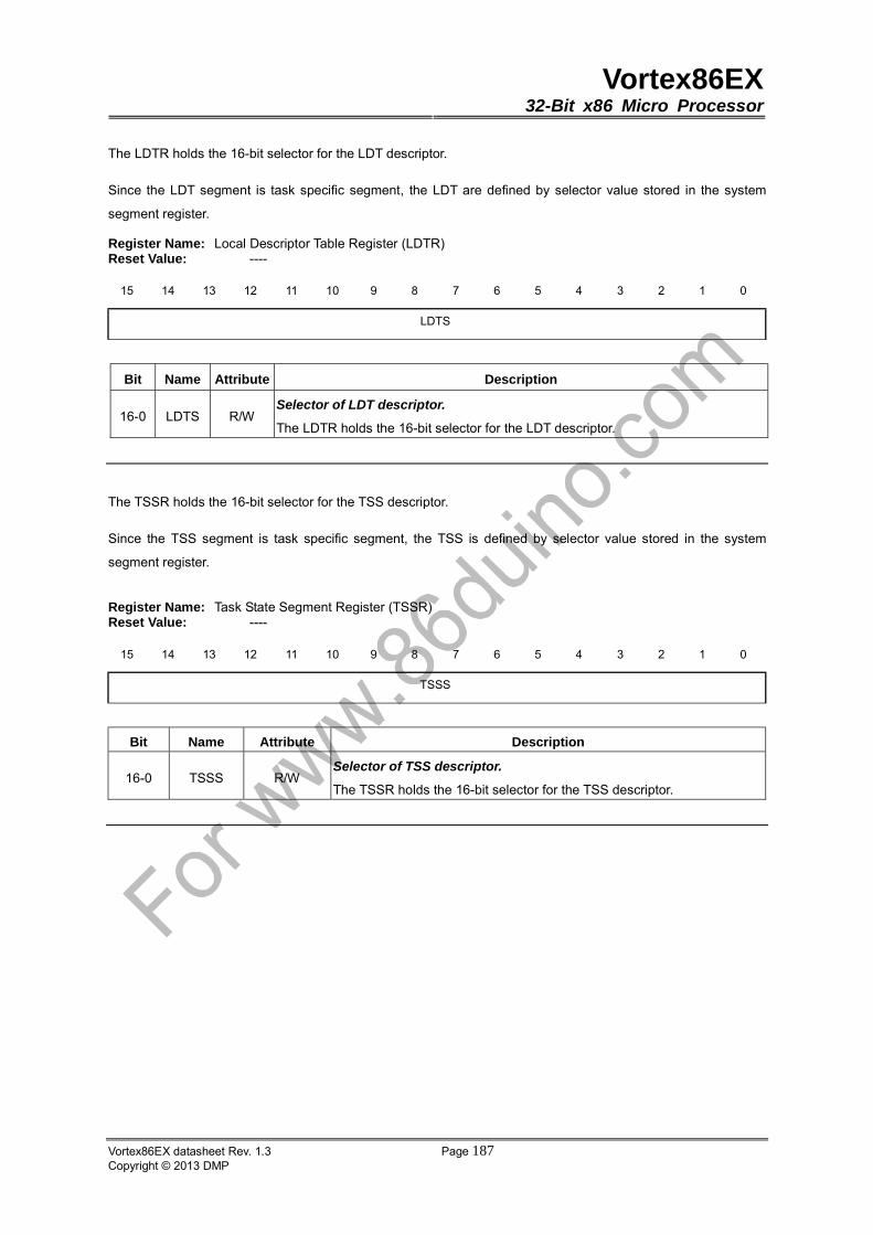
Vortex86EX32-Bit x86 Micro Processor
Vortex86EX datasheet Rev. 1.3 Page 187Copyright © 2013 DMP
The LDTR holds the 16-bit selector for the LDT descriptor.
Since the LDT segment is task specific segment, the LDT are defined by selector value stored in the system
segment register.
Register Name: Local Descriptor Table Register (LDTR) Reset Value: ----
15 14 13 12 11 10 9 8 7 6 5 4 3 2 1 0
LDTS
Bit Name Attribute Description
16-0 LDTS R/W Selector of LDT descriptor.
The LDTR holds the 16-bit selector for the LDT descriptor.
The TSSR holds the 16-bit selector for the TSS descriptor.
Since the TSS segment is task specific segment, the TSS is defined by selector value stored in the system
segment register.
Register Name: Task State Segment Register (TSSR) Reset Value: ----
15 14 13 12 11 10 9 8 7 6 5 4 3 2 1 0
TSSS
Bit Name Attribute Description
16-0 TSSS R/W Selector of TSS descriptor.
The TSSR holds the 16-bit selector for the TSS descriptor.

Vortex86EX32-Bit x86 Micro Processor
Vortex86EX datasheet Rev. 1.3 Page 188Copyright © 2013 DMP
11.1.7 FPU Registers
Register Name: FPU Data Register R0 Reset Value: --------
Double Extended-Precision Flatting Point.
79 78 64 63 0
Sig
nExponent Significand
Bit Name Attribute Description
79 Sign R/W Sign Bit.
78-64 Exp R/W Exponent.
63-0 Signd R/W Significand.
Double-Precision Flating Point
63 62 52 51 0
Sig
nExponent Significand
Bit Name Attribute Description
63 Sign R/W Sign Bit.
62-52 Exp R/W Exponent
51-0 Signd R/W Significand
Sigle-Precision Flating Point
31 30 29 28 27 26 25 24 23 22 21 20 19 18 17 16 15 14 13 12 11 10 9 8 7 6 5 4 3 2 1 0
Sig
nExponent Significand
Bit Name Attribute Description
31 Sign R/W Sign Bit.
30-23 Exp R/W Exponent.
22-0 Signd R/W Significand.

Vortex86EX32-Bit x86 Micro Processor
Vortex86EX datasheet Rev. 1.3 Page 189Copyright © 2013 DMP
Register Name: FPU Data Register R1 Reset Value: --------
Double Extended-Precision Flating Point
79 78 64 0
Sig
nExponent Significand
Bit Name Attribute Description
79 Sign R/W Sign Bit.
78-64 Exp R/W Exponent.
63-0 Signd R/W Significand.
Double-Precision Flating Point
63 62 52 51 0
Sig
nExponent Significand
Bit Name Attribute Description
63 Sign R/W Sign Bit.
62-52 Exp R/W Exponent.
51-0 Signd R/W Significand.
Sigle-Precision Flating Point
31 30 29 28 27 26 25 24 23 22 21 20 19 18 17 16 15 14 13 12 11 10 9 8 7 6 5 4 3 2 1 0
Sig
nExponent Significand
Bit Name Attribute Description
31 Sign R/W Sign Bit.
30-23 Exp R/W Exponent.
22-0 Signd R/W Significand.

Vortex86EX32-Bit x86 Micro Processor
Vortex86EX datasheet Rev. 1.3 Page 190Copyright © 2013 DMP
Register Name: FPU Data Register R2 Reset Value: --------
Double Extended-Precision Flating Point
79 78 64 63 0
Sig
nExponent Significand
Bit Name Attribute Description
79 Sign R/W Sign Bit.
78-64 Exp R/W Exponent.
63-0 Signd R/W Significand.
Double-Precision Flating Point
63 62 52 51 0
Sig
nExponent Significand
Bit Name Attribute Description
63 Sign R/W Sign Bit.
62-52 Exp R/W Exponent.
51-0 Signd R/W Significand.
Sigle-Precision Flating Point
31 30 29 28 27 26 25 24 23 22 21 20 19 18 17 16 15 14 13 12 11 10 9 8 7 6 5 4 3 2 1 0
Sig
nExponent Significand
Bit Name Attribute Description
31 Sign R/W Sign Bit.
30-23 Exp R/W Exponent.
22-0 Signd R/W Significand.

Vortex86EX32-Bit x86 Micro Processor
Vortex86EX datasheet Rev. 1.3 Page 191Copyright © 2013 DMP
Register Name: FPU Data Register R3 Reset Value: --------
Double Extended-Precision Flating Point
79 78 64 63 0
Sig
nExponent Significand
Bit Name Attribute Description
79 Sign R/W Sign Bit.
78-64 Exp R/W Exponent.
63-0 Signd R/W Significand.
Double-Precision Flating Point
63 62 52 51 0
Sig
nExponent Significand
Bit Name Attribute Description
63 Sign R/W Sign Bit.
62-52 Exp R/W Exponent.
51-0 Signd R/W Significand.
Sigle-Precision Flating Point
31 30 29 28 27 26 25 24 23 22 21 20 19 18 17 16 15 14 13 12 11 10 9 8 7 6 5 4 3 2 1 0
Sig
nExponent Significand
Bit Name Attribute Description
31 Sign R/W Sign Bit.
30-23 Exp R/W Exponent.
22-0 Signd R/W Significand.
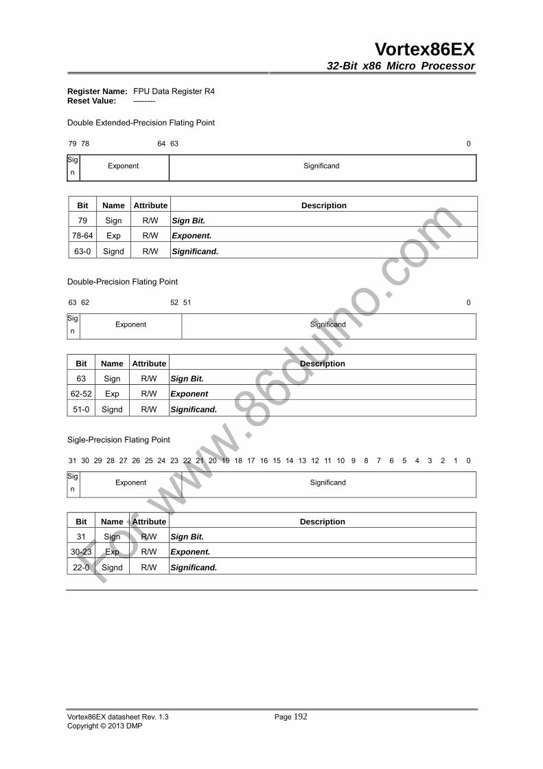
Vortex86EX32-Bit x86 Micro Processor
Vortex86EX datasheet Rev. 1.3 Page 192Copyright © 2013 DMP
Register Name: FPU Data Register R4 Reset Value: --------
Double Extended-Precision Flating Point
79 78 64 63 0
Sig
nExponent Significand
Bit Name Attribute Description
79 Sign R/W Sign Bit.
78-64 Exp R/W Exponent.
63-0 Signd R/W Significand.
Double-Precision Flating Point
63 62 52 51 0
Sig
nExponent Significand
Bit Name Attribute Description
63 Sign R/W Sign Bit.
62-52 Exp R/W Exponent
51-0 Signd R/W Significand.
Sigle-Precision Flating Point
31 30 29 28 27 26 25 24 23 22 21 20 19 18 17 16 15 14 13 12 11 10 9 8 7 6 5 4 3 2 1 0
Sig
nExponent Significand
Bit Name Attribute Description
31 Sign R/W Sign Bit.
30-23 Exp R/W Exponent.
22-0 Signd R/W Significand.

Vortex86EX32-Bit x86 Micro Processor
Vortex86EX datasheet Rev. 1.3 Page 193Copyright © 2013 DMP
Register Name: FPU Data Register R5 Reset Value: --------
Double Extended-Precision Flating Point
79 78 64 63 0
Sig
nExponent Significand
Bit Name Attribute Description
79 Sign R/W Sign Bit.
78-64 Exp R/W Exponent.
63-0 Signd R/W Significand.
Double-Precision Flating Point
63 62 52 51 0
Sig
nExponent Significand
Bit Name Attribute Description
63 Sign R/W Sign Bit.
62-52 Exp R/W Exponent.
51-0 Signd R/W Significand.
Sigle-Precision Flating Point
31 30 29 28 27 26 25 24 23 22 21 20 19 18 17 16 15 14 13 12 11 10 9 8 7 6 5 4 3 2 1 0
Sig
nExponent Significand
Bit Name Attribute Description
31 Sign R/W Sign Bit.
30-23 Exp R/W Exponent.
22-0 Signd R/W Significand.

Vortex86EX32-Bit x86 Micro Processor
Vortex86EX datasheet Rev. 1.3 Page 194Copyright © 2013 DMP
Register Name: FPU Data Register R6 Reset Value: --------
Double Extended-Precision Flating Point
79 78 64 63 0
Sig
nExponent Significand
Bit Name Attribute Description
79 Sign R/W Sign Bit.
78-64 Exp R/W Exponent.
63-0 Signd R/W Significand.
Double-Precision Flating Point
63 62 52 51 0
Sig
nExponent Significand
Bit Name Attribute Description
63 Sign R/W Sign Bit.
62-52 Exp R/W Exponent.
51-0 Signd R/W Significand.
Sigle-Precision Flating Point
31 30 29 28 27 26 25 24 23 22 21 20 19 18 17 16 15 14 13 12 11 10 9 8 7 6 5 4 3 2 1 0
Sig
nExponent Significand
Bit Name Attribute Description
31 Sign R/W Sign Bit.
30-23 Exp R/W Exponent.
22-0 Signd R/W Significand.

Vortex86EX32-Bit x86 Micro Processor
Vortex86EX datasheet Rev. 1.3 Page 195Copyright © 2013 DMP
Register Name: FPU Data Register R7 Reset Value: --------
Double Extended-Precision Flating Point
79 78 64 63 0
Sig
nExponent Significand
Bit Name Attribute Description
79 Sign R/W Sign Bit.
78-64 Exp R/W Exponent.
63-0 Signd R/W Significand.
Double-Precision Flating Point
63 62 52 51 0
Sig
nExponent Significand
Bit Name Attribute Description
63 Sign R/W Sign Bit.
62-52 Exp R/W Exponent.
51-0 Signd R/W Significand.
Sigle-Precision Flating Point
31 30 29 28 27 26 25 24 23 22 21 20 19 18 17 16 15 14 13 12 11 10 9 8 7 6 5 4 3 2 1 0
Sig
nExponent Significand
Bit Name Attribute Description
31 Sign R/W Sign Bit.
30-23 Exp R/W Exponent.
22-0 Signd R/W Significand.

Vortex86EX32-Bit x86 Micro Processor
Vortex86EX datasheet Rev. 1.3 Page 196Copyright © 2013 DMP
Register Name: X87 FPU Status Register Reset Value: ----
15 14 13 12 11 10 9 8 7 6 5 4 3 2 1 0
B C3 TOP C2 C1 C0 ES SF PE UE OE ZE DE IE
Bit Name Attribute Description
15 B R/W FPU Busy.
14 C3 R/W
Condition Code Flags.
The four condition code flags (C0 through C3) indicate the results of floating-point
comparison and arithmetic operations.
13-11 TOP R/W
Top of Stack (TOP) Pointer.
A pointer to the x87 FPU data register that is currently at the top of the x87 FPU
register stack.
10 C2 R/W
Condition Code Flags.
The four condition code flags (C0 through C3) indicate the results of floating-point
comparison and arithmetic operations.
9 C1 R/W
Condition Code Flags.
The four condition code flags (C0 through C3) indicate the results of floating-point
comparison and arithmetic operations.
8 C0 R/W
Condition Code Flags.
The four condition code flags (C0 through C3) indicate the results of floating-point
comparison and arithmetic operations.
7 ES R/W Error Summary Status.
6 SF R/W Stack Fault.
5 PE R/W Precision Exception Flags.
4 UE R/W Underflow Exception Flags.
3 OE R/W Overflow Exception Flags.
2 ZE R/W Zero Divide Exception Flags.
1 DE R/W Denormalized Operand Exception Flags.
0 IE R/W Invalid Operation Exception Flags.
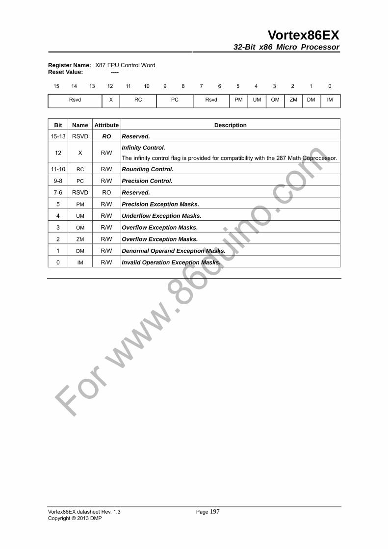
Vortex86EX32-Bit x86 Micro Processor
Vortex86EX datasheet Rev. 1.3 Page 197Copyright © 2013 DMP
Register Name: X87 FPU Control Word Reset Value: ----
15 14 13 12 11 10 9 8 7 6 5 4 3 2 1 0
Rsvd X RC PC Rsvd PM UM OM ZM DM IM
Bit Name Attribute Description
15-13 RSVD RO Reserved.
12 X R/W Infinity Control.
The infinity control flag is provided for compatibility with the 287 Math Coprocessor.
11-10 RC R/W Rounding Control.
9-8 PC R/W Precision Control.
7-6 RSVD RO Reserved.
5 PM R/W Precision Exception Masks.
4 UM R/W Underflow Exception Masks.
3 OM R/W Overflow Exception Masks.
2 ZM R/W Overflow Exception Masks.
1 DM R/W Denormal Operand Exception Masks.
0 IM R/W Invalid Operation Exception Masks.

Vortex86EX32-Bit x86 Micro Processor
Vortex86EX datasheet Rev. 1.3 Page 198Copyright © 2013 DMP
11.2 CPU MSR Registers
MSR Index: 10h MSR Name: Time-Stamp Counter Reset Value: 00000000_00000000h
63 0
TSC
Bit Name Attribute Description
63-0 TSC RO Time-Stamp Counter.
MSR Index: 174h MSR Name: IA32_SYSENTER_CS Reset Value: 00000000_00000000h
63 16 15 0
RSVD SETR_CS
Bit Name Attribute Description
63-16 RSVD RO Reserved.
15-0 SETR_CS R/W CS Selector for SYSENTER.
MSR Index: 175h MSR Name: IA32_SYSENTER_ESP Reset Value: 00000000_00000000h
63 32 31 0
RSVD SETR_ESP
Bit Name Attribute Description
63-32 RSVD RO Reserved.
31-0 SETR_ESP R/W ESP for for SYSENTER.

Vortex86EX32-Bit x86 Micro Processor
Vortex86EX datasheet Rev. 1.3 Page 199Copyright © 2013 DMP
MSR Index: 176h MSR Name: IA32_SYSENTER_EIP Reset Value: 00000000_00000000h
63 32 31 0
RSVD SETR_EIP
Bit Name Attribute Description
63-32 RSVD RO Reserved.
31-0 SETR_EIP R/W EIP for SYSENTER.
MSR Index: CFCFCF00h MSR Name: Reserved
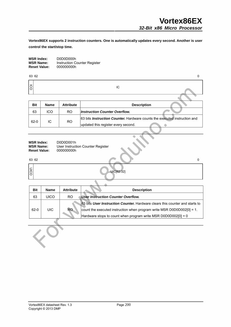
Vortex86EX32-Bit x86 Micro Processor
Vortex86EX datasheet Rev. 1.3 Page 200Copyright © 2013 DMP
Vortex86EX supports 2 instruction counters. One is automatically updates every second. Another is user
control the start/stop time.
MSR Index: D0D0D000h MSR Name: Instruction Counter Register Reset Value: 000000000h
63 62 0
IC
Bit Name Attribute Description
63 ICO RO Instruction Counter Overflow.
62-0 IC RO 63 bits Instruction Counter. Hardware counts the executed instruction and
updated this register every second.
MSR Index: D0D0D001h MSR Name: User Instruction Counter Register Reset Value: 000000000h
63 62 0
UIC[62:32]
Bit Name Attribute Description
63 UICO RO User Instruction Counter Overflow.
62-0 UIC RO
63 bits User Instruction Counter. Hardware clears this counter and starts to
count the executed instruction when program write MSR D0D0D002[0] = 1.
Hardware stops to count when program write MSR D0D0D002[0] = 0
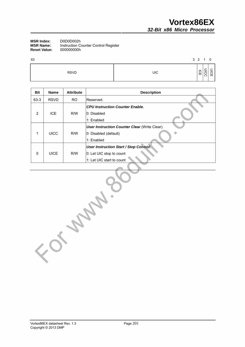
Vortex86EX32-Bit x86 Micro Processor
Vortex86EX datasheet Rev. 1.3 Page 201Copyright © 2013 DMP
MSR Index: D0D0D002h MSR Name: Instruction Counter Control Register Reset Value: 000000000h
63 3 2 1 0
RSVD UIC
Bit Name Attribute Description
63-3 RSVD RO Reserved.
2 ICE R/W
CPU Instruction Counter Enable.
0: Disabled
1: Enabled
1 UICC R/W
User Instruction Counter Clear (Write Clear).
0: Disabled (default)
1: Enabled
0 UICE R/W
User Instruction Start / Stop Control:
0: Let UIC stop to count
1: Let UIC start to count

Vortex86EX32-Bit x86 Micro Processor
Vortex86EX datasheet Rev. 1.3 Page 202Copyright © 2013 DMP
11.3 I / O Mapped Registers
11.3.1 PCI Configuration Registers
Configuration Address Register is a 32-bit register accessed only when referenced as a Dword. A byte or word
reference will pass through the Configuration Address Register onto the PCI bus as an I/O cycle.
I/O Port: CF8h ─ Accessed as a Dword Register Name: PCI Configuration Address Register Reset Value: 00000000h
31 30 29 28 27 26 25 24 23 22 21 20 19 18 17 16 15 14 13 12 11 10 9 8 7 6 5 4 3 2 1 0
CE RSVD BN DN FN RN RSVD
Bit Name Attribute Description
31 CE R/W
Configuration Enable.
When this bit is set to 1, accesses to PCI configuration space are enabled. If this bit
is reset to 0, accesses to PCI configuration space are disabled.
30-24 Rsvd RO Reserved.
23-16 BN R/W
Bus Number.
When the bus number is programmed to 00h, the target of the configuration cycle is
either the North-Bridge or the PCI Device that is connected to the North-Bridge. If
the bus number is programmed to 00h and the North-Bridge is not the target, a
Type 0 configuration cycle is generated on PCI Bus. IF the bus number is non-zero,
a Type 1 configuration cycle is generated on PCI bus with the bus number mapped
to AD[23:16] during the address phase.
15-11 DN R/W
Device Number.
This field selects one agent on the PCI bus. During a Type 1 configuration cycle,
this field is mapped to AD[15:11]. During a Type 0 configuration cycle, this field is
decoded and one of AD[31:11] is driven to 1.
10-8 FN R/W
Function Number.
This field allows the configuration registers of a particular function in a
multi-function device to be accessed. The SoC North Bridge only responds to
configuration cycle with a function number of 000b.
7-2 RN R/W
Register Number.
This field selects one register within a particular Bus, Device, and Function as
specified by the other fields in the Configuration Address Register.
1-0 Rsvd RO Reserved.
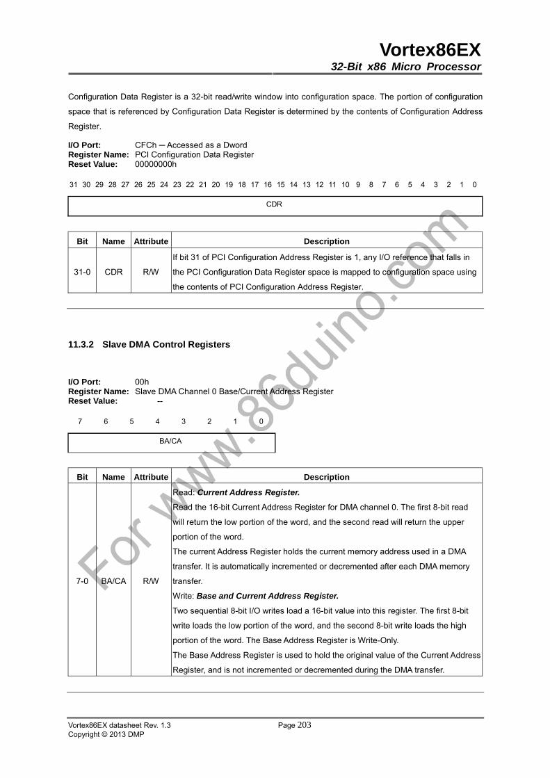
Vortex86EX32-Bit x86 Micro Processor
Vortex86EX datasheet Rev. 1.3 Page 203Copyright © 2013 DMP
Configuration Data Register is a 32-bit read/write window into configuration space. The portion of configuration
space that is referenced by Configuration Data Register is determined by the contents of Configuration Address
Register.
I/O Port: CFCh ─ Accessed as a Dword Register Name: PCI Configuration Data Register Reset Value: 00000000h
31 30 29 28 27 26 25 24 23 22 21 20 19 18 17 16 15 14 13 12 11 10 9 8 7 6 5 4 3 2 1 0
CDR
Bit Name Attribute Description
31-0 CDR R/W
If bit 31 of PCI Configuration Address Register is 1, any I/O reference that falls in
the PCI Configuration Data Register space is mapped to configuration space using
the contents of PCI Configuration Address Register.
11.3.2 Slave DMA Control Registers
I/O Port: 00h Register Name: Slave DMA Channel 0 Base/Current Address Register Reset Value: --
7 6 5 4 3 2 1 0
BA/CA
Bit Name Attribute Description
7-0 BA/CA R/W
Read: Current Address Register.
Read the 16-bit Current Address Register for DMA channel 0. The first 8-bit read
will return the low portion of the word, and the second read will return the upper
portion of the word.
The current Address Register holds the current memory address used in a DMA
transfer. It is automatically incremented or decremented after each DMA memory
transfer.
Write: Base and Current Address Register.
Two sequential 8-bit I/O writes load a 16-bit value into this register. The first 8-bit
write loads the low portion of the word, and the second 8-bit write loads the high
portion of the word. The Base Address Register is Write-Only.
The Base Address Register is used to hold the original value of the Current Address
Register, and is not incremented or decremented during the DMA transfer.
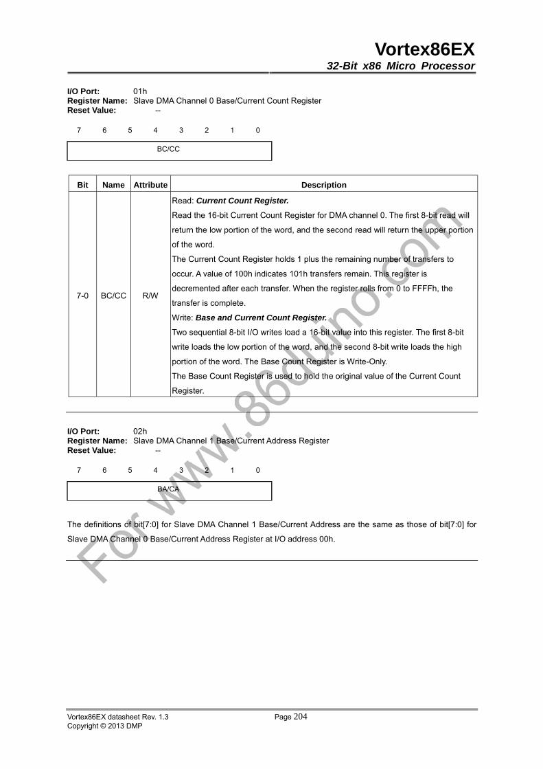
Vortex86EX32-Bit x86 Micro Processor
Vortex86EX datasheet Rev. 1.3 Page 204Copyright © 2013 DMP
I/O Port: 01h Register Name: Slave DMA Channel 0 Base/Current Count Register Reset Value: --
7 6 5 4 3 2 1 0
BC/CC
Bit Name Attribute Description
7-0 BC/CC R/W
Read: Current Count Register.
Read the 16-bit Current Count Register for DMA channel 0. The first 8-bit read will
return the low portion of the word, and the second read will return the upper portion
of the word.
The Current Count Register holds 1 plus the remaining number of transfers to
occur. A value of 100h indicates 101h transfers remain. This register is
decremented after each transfer. When the register rolls from 0 to FFFFh, the
transfer is complete.
Write: Base and Current Count Register.
Two sequential 8-bit I/O writes load a 16-bit value into this register. The first 8-bit
write loads the low portion of the word, and the second 8-bit write loads the high
portion of the word. The Base Count Register is Write-Only.
The Base Count Register is used to hold the original value of the Current Count
Register.
I/O Port: 02h Register Name: Slave DMA Channel 1 Base/Current Address Register Reset Value: --
7 6 5 4 3 2 1 0
BA/CA
The definitions of bit[7:0] for Slave DMA Channel 1 Base/Current Address are the same as those of bit[7:0] for
Slave DMA Channel 0 Base/Current Address Register at I/O address 00h.
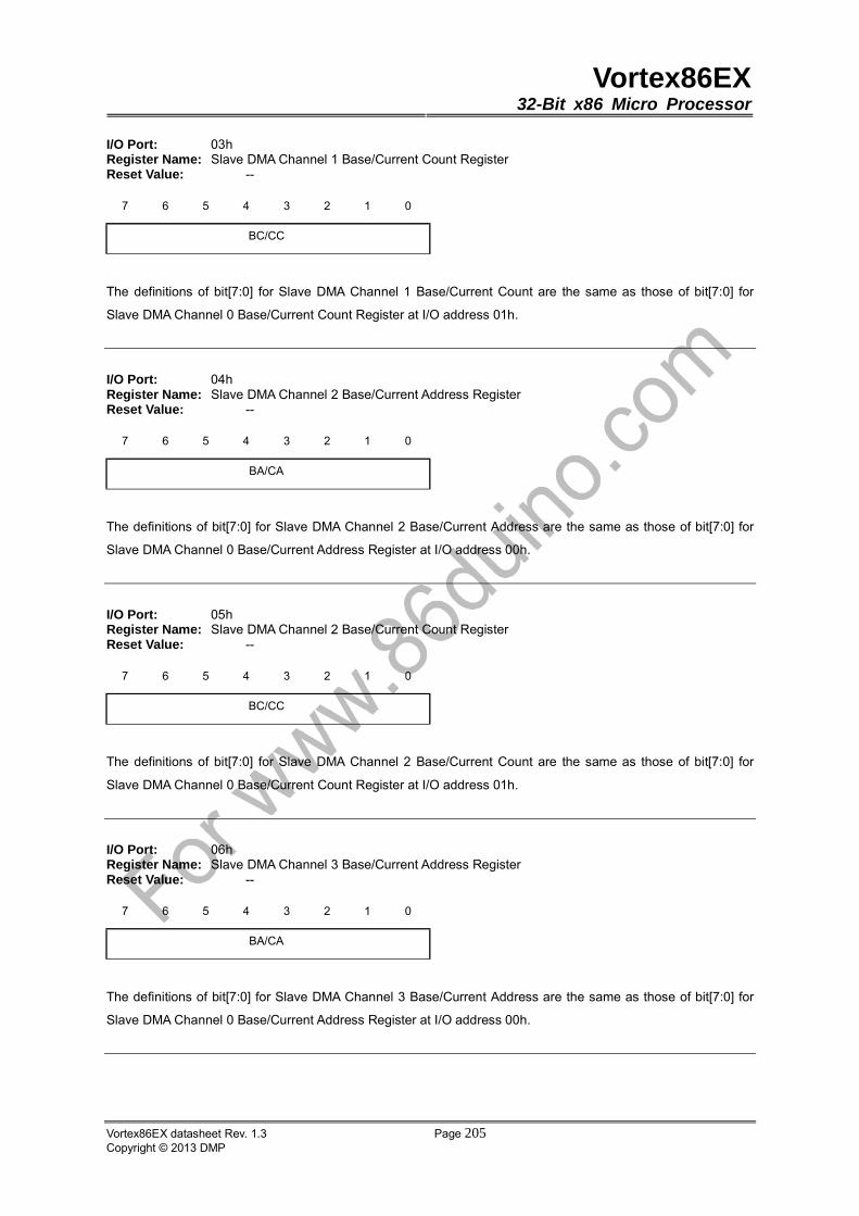
Vortex86EX32-Bit x86 Micro Processor
Vortex86EX datasheet Rev. 1.3 Page 205Copyright © 2013 DMP
I/O Port: 03h Register Name: Slave DMA Channel 1 Base/Current Count Register Reset Value: --
7 6 5 4 3 2 1 0
BC/CC
The definitions of bit[7:0] for Slave DMA Channel 1 Base/Current Count are the same as those of bit[7:0] for
Slave DMA Channel 0 Base/Current Count Register at I/O address 01h.
I/O Port: 04h Register Name: Slave DMA Channel 2 Base/Current Address Register Reset Value: --
7 6 5 4 3 2 1 0
BA/CA
The definitions of bit[7:0] for Slave DMA Channel 2 Base/Current Address are the same as those of bit[7:0] for
Slave DMA Channel 0 Base/Current Address Register at I/O address 00h.
I/O Port: 05h Register Name: Slave DMA Channel 2 Base/Current Count Register Reset Value: --
7 6 5 4 3 2 1 0
BC/CC
The definitions of bit[7:0] for Slave DMA Channel 2 Base/Current Count are the same as those of bit[7:0] for
Slave DMA Channel 0 Base/Current Count Register at I/O address 01h.
I/O Port: 06h Register Name: Slave DMA Channel 3 Base/Current Address Register Reset Value: --
7 6 5 4 3 2 1 0
BA/CA
The definitions of bit[7:0] for Slave DMA Channel 3 Base/Current Address are the same as those of bit[7:0] for
Slave DMA Channel 0 Base/Current Address Register at I/O address 00h.
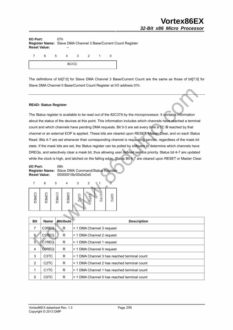
Vortex86EX32-Bit x86 Micro Processor
Vortex86EX datasheet Rev. 1.3 Page 206Copyright © 2013 DMP
I/O Port: 07h Register Name: Slave DMA Channel 3 Base/Current Count Register Reset Value: --
7 6 5 4 3 2 1 0
BC/CC
The definitions of bit[7:0] for Slave DMA Channel 3 Base/Current Count are the same as those of bit[7:0] for
Slave DMA Channel 0 Base/Current Count Register at I/O address 01h.
READ: Status Register
The Status register is available to be read out of the 82C37A by the microprocessor. It contains information
about the status of the devices at this point. This information includes which channels have reached a terminal
count and which channels have pending DMA requests. Bit 0-3 are set every time a TC is reached by that
channel or an external EOP is applied. These bits are cleared upon RESET, Master Clear, and on each Status
Read. Bits 4-7 are set whenever their corresponding channel is requesting service, regardless of the mask bit
state. If the mask bits are set, the Status register can be polled by software to determine which channels have
DREQs, and selectively clear a mask bit, thus allowing user defined service priority. Status bit 4-7 are updated
while the clock is high, and latched on the falling edge. Status Bit 4-7 are cleared upon RESET or Master Clear.
I/O Port: 08h Register Name: Slave DMA Command/Status Register Reset Value: 00000010b/00x0x0x0
7 6 5 4 3 2 1 0
Bit Name Attribute Description
7 C3REQ R = 1 DMA Channel 3 request
6 C2REQ R = 1 DMA Channel 2 request
5 C1REQ R = 1 DMA Channel 1 request
4 C0REQ R = 1 DMA Channel 0 request
3 C3TC R = 1 DMA Channel 3 has reached terminal count
2 C2TC R = 1 DMA Channel 2 has reached terminal count
1 C1TC R = 1 DMA Channel 1 has reached terminal count
0 C0TC R = 1 DMA Channel 0 has reached terminal count
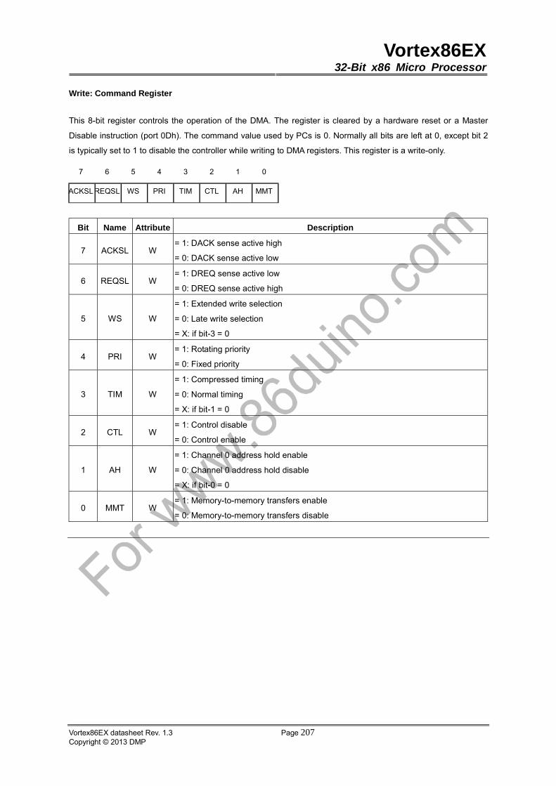
Vortex86EX32-Bit x86 Micro Processor
Vortex86EX datasheet Rev. 1.3 Page 207Copyright © 2013 DMP
Write: Command Register
This 8-bit register controls the operation of the DMA. The register is cleared by a hardware reset or a Master
Disable instruction (port 0Dh). The command value used by PCs is 0. Normally all bits are left at 0, except bit 2
is typically set to 1 to disable the controller while writing to DMA registers. This register is a write-only.
7 6 5 4 3 2 1 0
ACKSL REQSL WS PRI TIM CTL AH MMT
Bit Name Attribute Description
7 ACKSL W = 1: DACK sense active high
= 0: DACK sense active low
6 REQSL W = 1: DREQ sense active low
= 0: DREQ sense active high
5 WS W
= 1: Extended write selection
= 0: Late write selection
= X: if bit-3 = 0
4 PRI W = 1: Rotating priority
= 0: Fixed priority
3 TIM W
= 1: Compressed timing
= 0: Normal timing
= X: if bit-1 = 0
2 CTL W = 1: Control disable
= 0: Control enable
1 AH W
= 1: Channel 0 address hold enable
= 0: Channel 0 address hold disable
= X: if bit-0 = 0
0 MMT W = 1: Memory-to-memory transfers enable
= 0: Memory-to-memory transfers disable
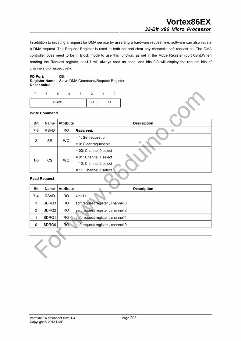
Vortex86EX32-Bit x86 Micro Processor
Vortex86EX datasheet Rev. 1.3 Page 208Copyright © 2013 DMP
In addition to initiating a request for DMA service by asserting a hardware request line, software can also initiate
a DMA request. The Request Register is used to both set and clear any channel’s soft request bit. The DMA
controller does need to be in Block mode to use this function, as set in the Mode Register (port 0Bh).When
reading the Request register, bits4-7 will always read as ones, and bits 0-3 will display the request bits of
channels 0-3 respectively.
I/O Port: 09h Register Name: Slave DMA Command/Request Register Reset Value: --
7 6 5 4 3 2 1 0
RSVD SR CS
Write Command
Bit Name Attribute Description
7-3 RSVD RO Reserved.
2 SR WO = 1: Set request bit
= 0: Clear request bit
1-0 CS WO
= 00: Channel 0 select
= 01: Channel 1 select
= 10: Channel 2 select
= 11: Channel 3 select
Read Request
Bit Name Attribute Description
7-4 RSVD RO 4’b1111
3 SDRQ3 RO soft request register , channel 3
2 SDRQ2 RO soft request register , channel 2
1 SDRQ1 RO soft request register , channel 1
0 SDRQ0 RO soft request register , channel 0
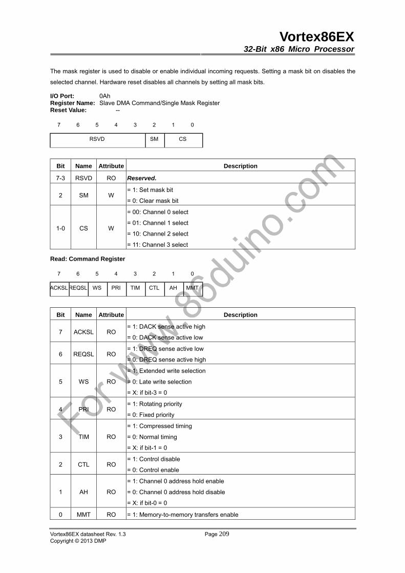
Vortex86EX32-Bit x86 Micro Processor
Vortex86EX datasheet Rev. 1.3 Page 209Copyright © 2013 DMP
The mask register is used to disable or enable individual incoming requests. Setting a mask bit on disables the
selected channel. Hardware reset disables all channels by setting all mask bits.
I/O Port: 0Ah Register Name: Slave DMA Command/Single Mask Register Reset Value: --
7 6 5 4 3 2 1 0
RSVD SM CS
Bit Name Attribute Description
7-3 RSVD RO Reserved.
2 SM W = 1: Set mask bit
= 0: Clear mask bit
1-0 CS W
= 00: Channel 0 select
= 01: Channel 1 select
= 10: Channel 2 select
= 11: Channel 3 select
Read: Command Register
7 6 5 4 3 2 1 0
ACKSL REQSL WS PRI TIM CTL AH MMT
Bit Name Attribute Description
7 ACKSL RO = 1: DACK sense active high
= 0: DACK sense active low
6 REQSL RO = 1: DREQ sense active low
= 0: DREQ sense active high
5 WS RO
= 1: Extended write selection
= 0: Late write selection
= X: if bit-3 = 0
4 PRI RO = 1: Rotating priority
= 0: Fixed priority
3 TIM RO
= 1: Compressed timing
= 0: Normal timing
= X: if bit-1 = 0
2 CTL RO = 1: Control disable
= 0: Control enable
1 AH RO
= 1: Channel 0 address hold enable
= 0: Channel 0 address hold disable
= X: if bit-0 = 0
0 MMT RO = 1: Memory-to-memory transfers enable

Vortex86EX32-Bit x86 Micro Processor
Vortex86EX datasheet Rev. 1.3 Page 210Copyright © 2013 DMP
Bit Name Attribute Description
= 0: Memory-to-memory transfers disable
The Mode Register indicates the mode of operation for each of the four DMA channels 0 to 3. Each channel has
a separate 6-bit mode register and each is loaded through the Mode Register port.
I/O Port: 0Bh Register Name: Slave DMA Mode Register Reset Value: --
7 6 5 4 3 2 1 0
MT AD/AI ATI TT CS
Bit Name Attribute Description
7-6 MT W
Mode Type Selection.
= 00: Demand mode
= 01: Single mode
= 10: Block mode
= 11: Cascade mode
5 AD/AI W = 1: Address decrement select
= 0: Address increment select
4 ATI W = 1: Auto initialization enable
= 0: Auto initialization disable
3-2 TT W
Transfer Type.
= 00: Verify operation
= 01: Write operation
= 10: Read operation
= 11: not valid
= xx: if they are in cascade mode (bit 6 & 7)
1-0 CS W
Channel Selection.
= 00: Channel 0 select
= 01: Channel 1 select
= 10: Channel 2 select
= 11: Channel 3 select
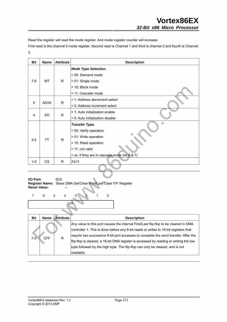
Vortex86EX32-Bit x86 Micro Processor
Vortex86EX datasheet Rev. 1.3 Page 211Copyright © 2013 DMP
Read the register will read the mode register. And mode register counter will increase.
First read is the channel 0 mode register. Second read is Channel 1 and third is channel 2 and fourth is Channel
3.
Bit Name Attribute Description
7-6 MT R
Mode Type Selection.
= 00: Demand mode
= 01: Single mode
= 10: Block mode
= 11: Cascade mode
5 AD/AI R = 1: Address decrement select
= 0: Address increment select
4 ATI R = 1: Auto initialization enable
= 0: Auto initialization disable
3-2 TT R
Transfer Type.
= 00: Verify operation
= 01: Write operation
= 10: Read operation
= 11: not valid
= xx: if they are in cascade mode (bit 6 & 7)
1-0 CS R 2’b11
I/O Port: 0Ch Register Name: Slave DMA Set/Clear First/Last Clear F/F Register Reset Value: --
7 6 5 4 3 2 1 0
CFF
Bit Name Attribute Description
7-0 CFF R
Any value to this port causes the internal First/Last flip-flop to be cleared in DMA
controller 1. This is done before any 8-bit reads or writes to 16-bit registers that
require two successive 8-bit port accesses to complete the word transfer. After the
flip-flop is cleared, a 16-bit DMA register is accessed by reading or writing the low
byte followed by the high byte. The flip-flop can only be cleared, and is not
readable.
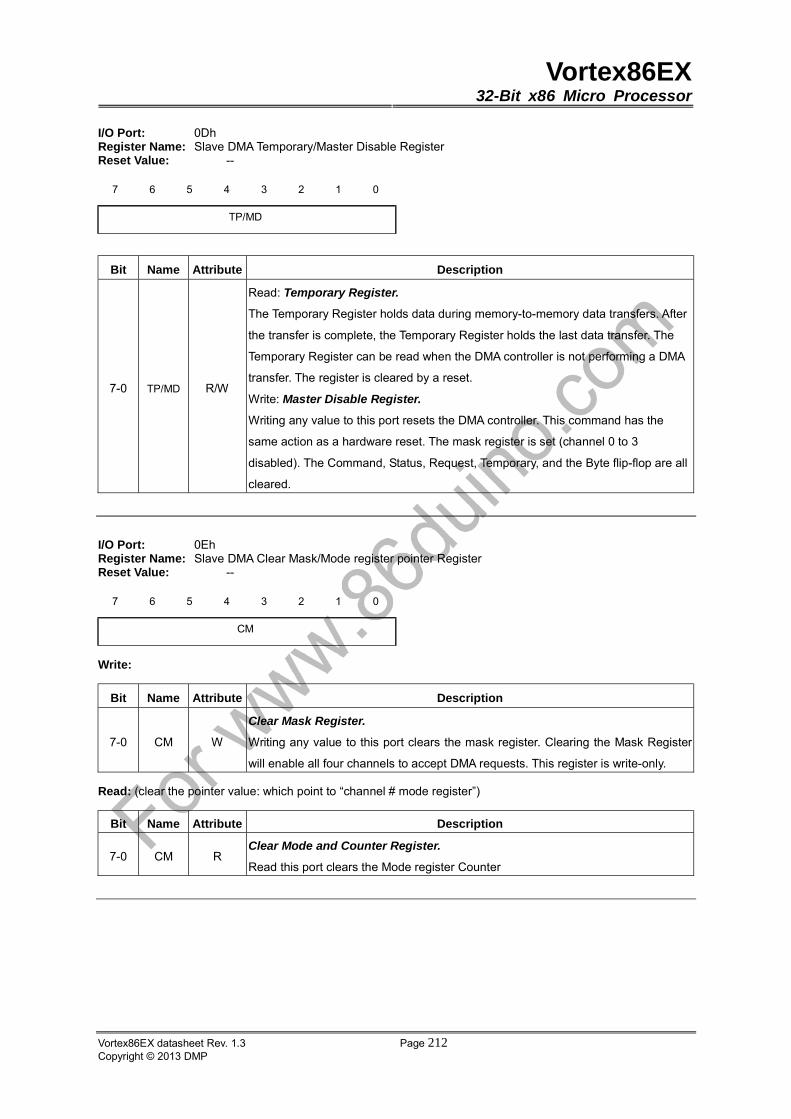
Vortex86EX32-Bit x86 Micro Processor
Vortex86EX datasheet Rev. 1.3 Page 212Copyright © 2013 DMP
I/O Port: 0Dh Register Name: Slave DMA Temporary/Master Disable Register Reset Value: --
7 6 5 4 3 2 1 0
TP/MD
Bit Name Attribute Description
7-0 TP/MD R/W
Read: Temporary Register.
The Temporary Register holds data during memory-to-memory data transfers. After
the transfer is complete, the Temporary Register holds the last data transfer. The
Temporary Register can be read when the DMA controller is not performing a DMA
transfer. The register is cleared by a reset.
Write: Master Disable Register.
Writing any value to this port resets the DMA controller. This command has the
same action as a hardware reset. The mask register is set (channel 0 to 3
disabled). The Command, Status, Request, Temporary, and the Byte flip-flop are all
cleared.
I/O Port: 0Eh Register Name: Slave DMA Clear Mask/Mode register pointer Register Reset Value: --
7 6 5 4 3 2 1 0
CM
Write:
Bit Name Attribute Description
7-0 CM W
Clear Mask Register.
Writing any value to this port clears the mask register. Clearing the Mask Register
will enable all four channels to accept DMA requests. This register is write-only.
Read: (clear the pointer value: which point to “channel # mode register”)
Bit Name Attribute Description
7-0 CM R Clear Mode and Counter Register.
Read this port clears the Mode register Counter
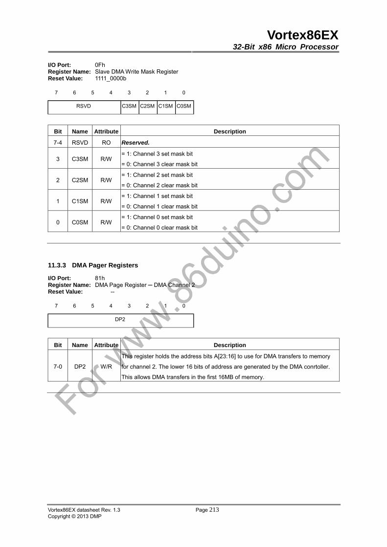
Vortex86EX32-Bit x86 Micro Processor
Vortex86EX datasheet Rev. 1.3 Page 213Copyright © 2013 DMP
I/O Port: 0Fh Register Name: Slave DMA Write Mask Register Reset Value: 1111_0000b
7 6 5 4 3 2 1 0
RSVD C3SM C2SM C1SM C0SM
Bit Name Attribute Description
7-4 RSVD RO Reserved.
3 C3SM R/W = 1: Channel 3 set mask bit
= 0: Channel 3 clear mask bit
2 C2SM R/W = 1: Channel 2 set mask bit
= 0: Channel 2 clear mask bit
1 C1SM R/W = 1: Channel 1 set mask bit
= 0: Channel 1 clear mask bit
0 C0SM R/W = 1: Channel 0 set mask bit
= 0: Channel 0 clear mask bit
11.3.3 DMA Pager Registers
I/O Port: 81h Register Name: DMA Page Register ─ DMA Channel 2 Reset Value: --
7 6 5 4 3 2 1 0
DP2
Bit Name Attribute Description
7-0 DP2 W/R
This register holds the address bits A[23:16] to use for DMA transfers to memory
for channel 2. The lower 16 bits of address are generated by the DMA conrtoller.
This allows DMA transfers in the first 16MB of memory.
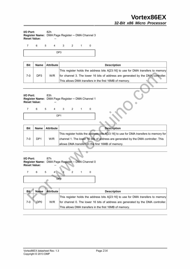
Vortex86EX32-Bit x86 Micro Processor
Vortex86EX datasheet Rev. 1.3 Page 214Copyright © 2013 DMP
I/O Port: 82h Register Name: DMA Page Register ─ DMA Channel 3 Reset Value: --
7 6 5 4 3 2 1 0
DP3
Bit Name Attribute Description
7-0 DP3 W/R
This register holds the address bits A[23:16] to use for DMA transfers to memory
for channel 3. The lower 16 bits of address are generated by the DMA controller.
This allows DMA transfers in the first 16MB of memory.
I/O Port: 83h Register Name: DMA Page Register ─ DMA Channel 1 Reset Value: --
7 6 5 4 3 2 1 0
DP1
Bit Name Attribute Description
7-0 DP1 W/R
This register holds the address bits A[23:16] to use for DMA transfers to memory for
channel 1. The lower 16 bits of address are generated by the DMA controller. This
allows DMA transfers in the first 16MB of memory.
I/O Port: 87h Register Name: DMA Page Register ─ DMA Channel 0 Reset Value: --
7 6 5 4 3 2 1 0
DP0
Bit Name Attribute Description
7-0 DP0 W/R
This register holds the address bits A[23:16] to use for DMA transfers to memory
for channel 0. The lower 16 bits of address are generated by the DMA controller.
This allows DMA transfers in the first 16MB of memory.
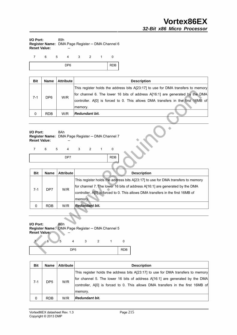
Vortex86EX32-Bit x86 Micro Processor
Vortex86EX datasheet Rev. 1.3 Page 215Copyright © 2013 DMP
I/O Port: 89h Register Name: DMA Page Register ─ DMA Channel 6 Reset Value: --
7 6 5 4 3 2 1 0
DP6 RDB
Bit Name Attribute Description
7-1 DP6 W/R
This register holds the address bits A[23:17] to use for DMA transfers to memory
for channel 6. The lower 16 bits of address A[16:1] are generated by the DMA
controller. A[0] is forced to 0. This allows DMA transfers in the first 16MB of
memory.
0 RDB W/R Redundant bit.
I/O Port: 8Ah Register Name: DMA Page Register ─ DMA Channel 7 Reset Value: --
7 6 5 4 3 2 1 0
DP7 RDB
Bit Name Attribute Description
7-1 DP7 W/R
This register holds the address bits A[23:17] to use for DMA transfers to memory
for channel 7. The lower 16 bits of address A[16:1] are generated by the DMA
controller, A[0] is forced to 0. This allows DMA transfers in the first 16MB of
memory.
0 RDB W/R Redundant bit.
I/O Port: 8Bh Register Name: DMA Page Register ─ DMA Channel 5 Reset Value: --
7 6 5 4 3 2 1 0
DP5 RDB
Bit Name Attribute Description
7-1 DP5 W/R
This register holds the address bits A[23:17] to use for DMA transfers to memory
for channel 5. The lower 16 bits of address A[16:1] are generated by the DMA
controller, A[0] is forced to 0. This allows DMA transfers in the first 16MB of
memory.
0 RDB W/R Redundant bit.

Vortex86EX32-Bit x86 Micro Processor
Vortex86EX datasheet Rev. 1.3 Page 216Copyright © 2013 DMP
11.3.4 Master DMA Control Registers
I/O Port: C0h Register Name: Master DMA Channel 4 Base/Current Address Register Reset Value: --
7 6 5 4 3 2 1 0
BA/CA
Bit Name Attribute Description
7-0 BA/CA R/W DMA Channel 4 is used for a cascade function from slave DMA. Channel 4 is
unavailable for other uses.
I/O Port: C2h Register Name: Master DMA Channel 4 Base/Current Count Register Reset Value: --
7 6 5 4 3 2 1 0
BC/CC
Bit Name Attribute Description
7-0 BC/CC R/W DMA Channel 4 is used for a cascade function from slave DMA. Channel 4 is
unavailable for other uses.
I/O Port: C4h Register Name: Master DMA Channel 5 Base/Current Address Register Reset Value: --
7 6 5 4 3 2 1 0
BA/CA
On AT and EISA systems, DMA channel 5 is an unassigned channel, used for high-speed transfers between
memory and the I/O bus. On PS/2, channel 5 is used for hard disk DMA operations.
The definitions of bit[7:0] for Master DMA Channel 5 Base/Current Count are the same as those of bit[7:0] for
Slave DMA Channel 0 Base/Current Count Register at I/O address 00h.
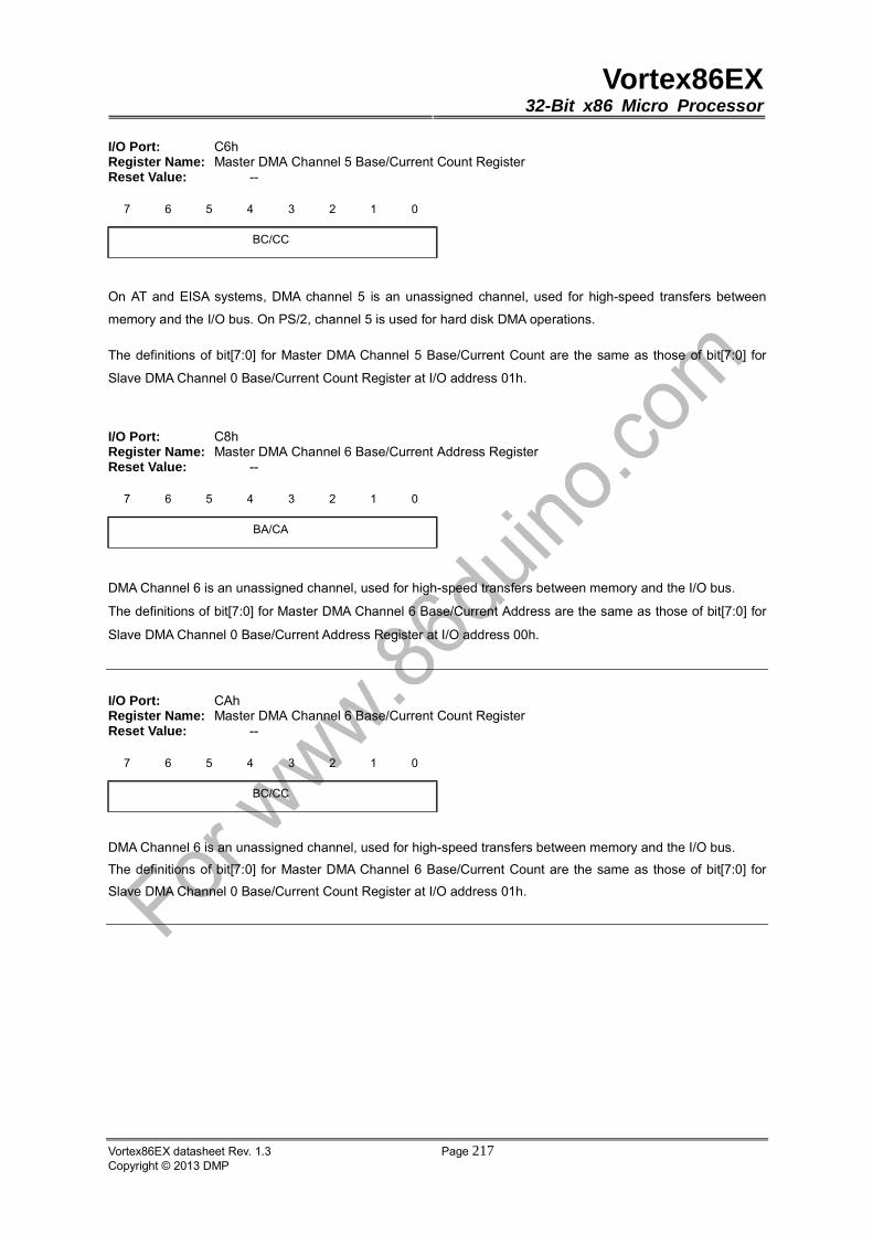
Vortex86EX32-Bit x86 Micro Processor
Vortex86EX datasheet Rev. 1.3 Page 217Copyright © 2013 DMP
I/O Port: C6h Register Name: Master DMA Channel 5 Base/Current Count Register Reset Value: --
7 6 5 4 3 2 1 0
BC/CC
On AT and EISA systems, DMA channel 5 is an unassigned channel, used for high-speed transfers between
memory and the I/O bus. On PS/2, channel 5 is used for hard disk DMA operations.
The definitions of bit[7:0] for Master DMA Channel 5 Base/Current Count are the same as those of bit[7:0] for
Slave DMA Channel 0 Base/Current Count Register at I/O address 01h.
I/O Port: C8h Register Name: Master DMA Channel 6 Base/Current Address Register Reset Value: --
7 6 5 4 3 2 1 0
BA/CA
DMA Channel 6 is an unassigned channel, used for high-speed transfers between memory and the I/O bus.
The definitions of bit[7:0] for Master DMA Channel 6 Base/Current Address are the same as those of bit[7:0] for
Slave DMA Channel 0 Base/Current Address Register at I/O address 00h.
I/O Port: CAh Register Name: Master DMA Channel 6 Base/Current Count Register Reset Value: --
7 6 5 4 3 2 1 0
BC/CC
DMA Channel 6 is an unassigned channel, used for high-speed transfers between memory and the I/O bus.
The definitions of bit[7:0] for Master DMA Channel 6 Base/Current Count are the same as those of bit[7:0] for
Slave DMA Channel 0 Base/Current Count Register at I/O address 01h.
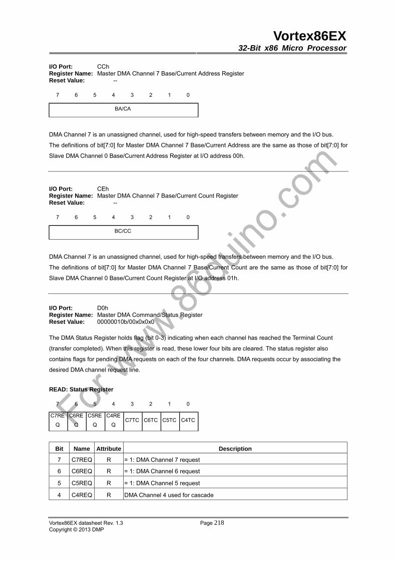
Vortex86EX32-Bit x86 Micro Processor
Vortex86EX datasheet Rev. 1.3 Page 218Copyright © 2013 DMP
I/O Port: CCh Register Name: Master DMA Channel 7 Base/Current Address Register Reset Value: --
7 6 5 4 3 2 1 0
BA/CA
DMA Channel 7 is an unassigned channel, used for high-speed transfers between memory and the I/O bus.
The definitions of bit[7:0] for Master DMA Channel 7 Base/Current Address are the same as those of bit[7:0] for
Slave DMA Channel 0 Base/Current Address Register at I/O address 00h.
I/O Port: CEh Register Name: Master DMA Channel 7 Base/Current Count Register Reset Value: --
7 6 5 4 3 2 1 0
BC/CC
DMA Channel 7 is an unassigned channel, used for high-speed transfers between memory and the I/O bus.
The definitions of bit[7:0] for Master DMA Channel 7 Base/Current Count are the same as those of bit[7:0] for
Slave DMA Channel 0 Base/Current Count Register at I/O address 01h.
I/O Port: D0h Register Name: Master DMA Command/Status Register Reset Value: 00000010b/00x0x0x0
The DMA Status Register holds flag (bit 0-3) indicating when each channel has reached the Terminal Count
(transfer completed). When this register is read, these lower four bits are cleared. The status register also
contains flags for pending DMA requests on each of the four channels. DMA requests occur by associating the
desired DMA channel request line.
READ: Status Register
7 6 5 4 3 2 1 0
C7RE
Q
C6RE
Q
C5RE
Q
C4RE
Q C7TC C6TC C5TC C4TC
Bit Name Attribute Description
7 C7REQ R = 1: DMA Channel 7 request
6 C6REQ R = 1: DMA Channel 6 request
5 C5REQ R = 1: DMA Channel 5 request
4 C4REQ R DMA Channel 4 used for cascade

Vortex86EX32-Bit x86 Micro Processor
Vortex86EX datasheet Rev. 1.3 Page 219Copyright © 2013 DMP
3 C7TC R = 1: DMA Channel 7 has reached terminal count
2 C6TC R = 1: DMA Channel 6 has reached terminal count
1 C5TC R = 1: DMA Channel 5 has reached terminal count
0 C4TC R DMA Channel 4 used for cascade
Write: Command Register
This 8-bit register controls the operation of the DMA. The register is cleared by a hardware reset or a Master
Disable instruction (port DAh). The command value used by PCs is 0. Normally all bits are left at 0, except bit 2
is typically set to 1 to disable the controller while writing to DMA registers. This register is write-only.
7 6 5 4 3 2 1 0
ACKSL REQSL WS PRI TIM CTL AH MMT
Bit Name Attribute Description
7 ACKSL W = 1: DACK sense active high
= 0: DACK sense active low
6 REQSL W = 1: DREQ sense active low
= 0: DREQ sense active high
5 WS W
= 1: Extended write selection
= 0: Late write selection
= X: if bit 3 = 0
4 PRI W = 1: Rotating priority
= 0: Fixed priority
3 TIM W
= 1: Compressed timing
= 0: Normal timing
= X: if bit 1 = 0
2 CTL W = 1: Control disable
= 0: Control enable
1 AH W
= 1: Channel 4 address hold enable
= 0: Channel 4 address hold disable
= X: if bit 0 = 0
0 MMT W = 1: Memory-to-memory transfers enable
= 0: Memory-to-memory transfers disable

Vortex86EX32-Bit x86 Micro Processor
Vortex86EX datasheet Rev. 1.3 Page 220Copyright © 2013 DMP
In addition to initiating a request for DMA service by asserting a hardware request line, software can also initiate
a DMA request. The Request Register is used to both set and clear any channel’s soft request bit. The DMA
controller does need to be in Block mode to use this function, as set in the Mode Register (port D6h).When
reading the Request register, bits4-7 will always read as ones, and bits 0-3 will display the request bits of
channels 4-7 respectively
I/O Port: D2h Register Name: Master DMA Command/Request Register Reset Value: --
7 6 5 4 3 2 1 0
RSVD SR CS
WRITE Command
Bit Name Attribute Description
7-3 Rsvd RO Reserved.
2 SR W = 1: Set request bit
= 0: Clear request bit
1-0 CS W
= 00: Channel 4 select
= 01: Channel 5 select
= 10: Channel 6 select
= 11: Channel 7 select
READ Request
Bit Name Attribute Description
7-4 RSVD RO 4’b1111
3 SDRQ7 RO soft request register , channel 7
2 SDRQ6 RO soft request register , channel 6
1 SDRQ5 RO soft request register , channel 5
0 SDRQ4 RO soft request register , channel 4
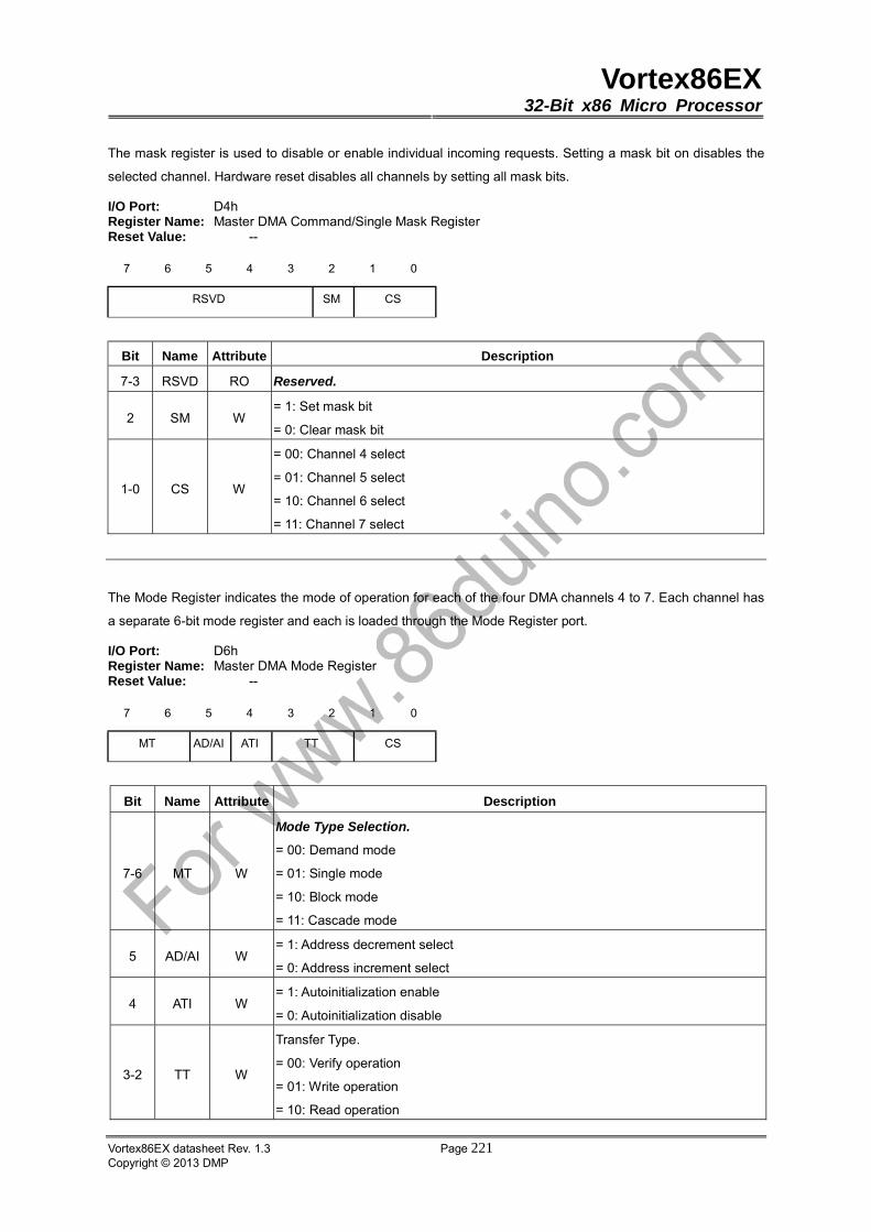
Vortex86EX32-Bit x86 Micro Processor
Vortex86EX datasheet Rev. 1.3 Page 221Copyright © 2013 DMP
The mask register is used to disable or enable individual incoming requests. Setting a mask bit on disables the
selected channel. Hardware reset disables all channels by setting all mask bits.
I/O Port: D4h Register Name: Master DMA Command/Single Mask Register Reset Value: --
7 6 5 4 3 2 1 0
RSVD SM CS
Bit Name Attribute Description
7-3 RSVD RO Reserved.
2 SM W = 1: Set mask bit
= 0: Clear mask bit
1-0 CS W
= 00: Channel 4 select
= 01: Channel 5 select
= 10: Channel 6 select
= 11: Channel 7 select
The Mode Register indicates the mode of operation for each of the four DMA channels 4 to 7. Each channel has
a separate 6-bit mode register and each is loaded through the Mode Register port.
I/O Port: D6h Register Name: Master DMA Mode Register Reset Value: --
7 6 5 4 3 2 1 0
MT AD/AI ATI TT CS
Bit Name Attribute Description
7-6 MT W
Mode Type Selection.
= 00: Demand mode
= 01: Single mode
= 10: Block mode
= 11: Cascade mode
5 AD/AI W = 1: Address decrement select
= 0: Address increment select
4 ATI W = 1: Autoinitialization enable
= 0: Autoinitialization disable
3-2 TT W
Transfer Type.
= 00: Verify operation
= 01: Write operation
= 10: Read operation
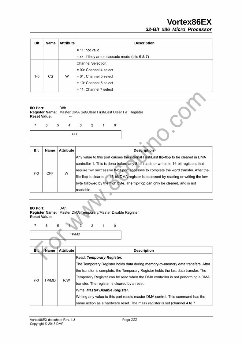
Vortex86EX32-Bit x86 Micro Processor
Vortex86EX datasheet Rev. 1.3 Page 222Copyright © 2013 DMP
Bit Name Attribute Description
= 11: not valid
= xx: if they are in cascade mode (bits 6 & 7)
1-0 CS W
Channel Selection.
= 00: Channel 4 select
= 01: Channel 5 select
= 10: Channel 6 select
= 11: Channel 7 select
I/O Port: D8h Register Name: Master DMA Set/Clear First/Last Clear F/F Register Reset Value: --
7 6 5 4 3 2 1 0
CFF
Bit Name Attribute Description
7-0 CFF W
Any value to this port causes the internal First/Last flip-flop to be cleared in DMA
controller 1. This is done before any 8-bit reads or writes to 16-bit registers that
require two successive 8-bit port accesses to complete the word transfer. After the
flip-flop is cleared, a 16-bit DMA register is accessed by reading or writing the low
byte followed by the high byte. The flip-flop can only be cleared, and is not
readable.
I/O Port: DAh Register Name: Master DMA Temporary/Master Disable Register Reset Value: --
7 6 5 4 3 2 1 0
TP/MD
Bit Name Attribute Description
7-0 TP/MD R/W
Read: Temporary Register.
The Temporary Register holds data during memory-to-memory data transfers. After
the transfer is complete, the Temporary Register holds the last data transfer. The
Temporary Register can be read when the DMA controller is not performing a DMA
transfer. The register is cleared by a reset.
Write: Master Disable Register.
Writing any value to this port resets master DMA control. This command has the
same action as a hardware reset. The mask register is set (channel 4 to 7

Vortex86EX32-Bit x86 Micro Processor
Vortex86EX datasheet Rev. 1.3 Page 223Copyright © 2013 DMP
disabled). The Command, Status, Request, Temporary, and the Byte flip-flop are all
cleared.
I/O Port: DCh Register Name: Master DMA Clear Mask/Mode register pointer Register Reset Value: --
7 6 5 4 3 2 1 0
CM
WRITE:
Bit Name Attribute Description
7-0 CM W
Clear Mask Register.
Writing any value to this port clears the mask register. Clearing the Mask Register
will enable all four channels to accept DMA requests. This register is write-only.
READ: (clear the pointer value: which point to “channel # mode register”)
Bit Name Attribute Description
7-0 CM R Clear Mode and Counter Register
Read this port clears the Mode register Counter
The mask register is used to disable or enable individual incoming requests. Setting a mask bit on disables the
selected channel. A hardware reset disables all channels by setting all mask bits.
I/O Port: DEh Register Name: Master DMA Write Mask Register Reset Value: xxxx_0000b
7 6 5 4 3 2 1 0
RSVD C7SM C6SM C5SM C4SM
Bit Name Attribute Description
7-4 RSVD RO Reserved.
3 C7SM W = 1: Channel 7 sets mask bit
= 0: Channel 7 clears mask bit
2 C6SM W = 1: Channel 6 sets mask bit
= 0: Channel 6 clears mask bit
1 C5SM W = 1: Channel 5 sets mask bit
= 0: Channel 5 clears mask bit
0 C4SM W = 1: Channel 4 sets mask bit
= 0: Channel 4 clears mask bit
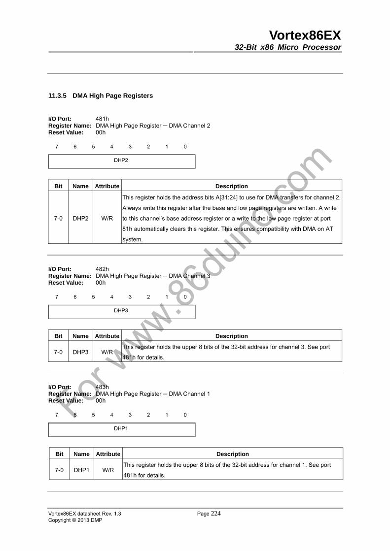
Vortex86EX32-Bit x86 Micro Processor
Vortex86EX datasheet Rev. 1.3 Page 224Copyright © 2013 DMP
11.3.5 DMA High Page Registers
I/O Port: 481h Register Name: DMA High Page Register ─ DMA Channel 2 Reset Value: 00h
7 6 5 4 3 2 1 0
DHP2
Bit Name Attribute Description
7-0 DHP2 W/R
This register holds the address bits A[31:24] to use for DMA transfers for channel 2.
Always write this register after the base and low page registers are written. A write
to this channel’s base address register or a write to the low page register at port
81h automatically clears this register. This ensures compatibility with DMA on AT
system.
I/O Port: 482h Register Name: DMA High Page Register ─ DMA Channel 3 Reset Value: 00h
7 6 5 4 3 2 1 0
DHP3
Bit Name Attribute Description
7-0 DHP3 W/R This register holds the upper 8 bits of the 32-bit address for channel 3. See port
481h for details.
I/O Port: 483h Register Name: DMA High Page Register ─ DMA Channel 1 Reset Value: 00h
7 6 5 4 3 2 1 0
DHP1
Bit Name Attribute Description
7-0 DHP1 W/R This register holds the upper 8 bits of the 32-bit address for channel 1. See port
481h for details.
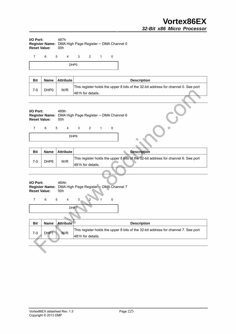
Vortex86EX32-Bit x86 Micro Processor
Vortex86EX datasheet Rev. 1.3 Page 225Copyright © 2013 DMP
I/O Port: 487h Register Name: DMA High Page Register ─ DMA Channel 0 Reset Value: 00h
7 6 5 4 3 2 1 0
DHP0
Bit Name Attribute Description
7-0 DHP0 W/R This register holds the upper 8 bits of the 32-bit address for channel 0. See port
481h for details.
I/O Port: 489h Register Name: DMA High Page Register ─ DMA Channel 6 Reset Value: 00h
7 6 5 4 3 2 1 0
DHP6
Bit Name Attribute Description
7-0 DHP6 W/R This register holds the upper 8 bits of the 32-bit address for channel 6. See port
481h for details.
I/O Port: 48Ah Register Name: DMA High Page Register ─ DMA Channel 7 Reset Value: 00h
7 6 5 4 3 2 1 0
DHP7
Bit Name Attribute Description
7-0 DHP7 W/R This register holds the upper 8 bits of the 32-bit address for channel 7. See port
481h for details.
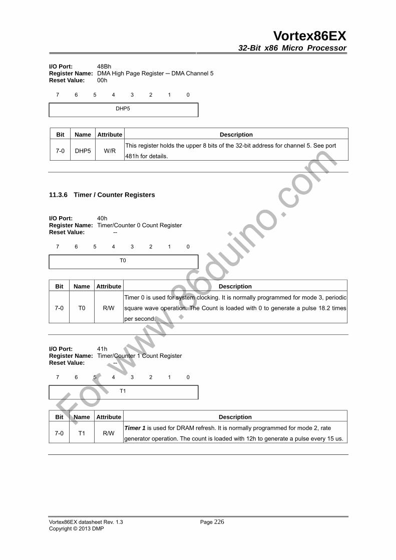
Vortex86EX32-Bit x86 Micro Processor
Vortex86EX datasheet Rev. 1.3 Page 226Copyright © 2013 DMP
I/O Port: 48Bh Register Name: DMA High Page Register ─ DMA Channel 5 Reset Value: 00h
7 6 5 4 3 2 1 0
DHP5
Bit Name Attribute Description
7-0 DHP5 W/R This register holds the upper 8 bits of the 32-bit address for channel 5. See port
481h for details.
11.3.6 Timer / Counter Registers
I/O Port: 40h Register Name: Timer/Counter 0 Count Register Reset Value: --
7 6 5 4 3 2 1 0
T0
Bit Name Attribute Description
7-0 T0 R/W
Timer 0 is used for system clocking. It is normally programmed for mode 3, periodic
square wave operation. The Count is loaded with 0 to generate a pulse 18.2 times
per second.
I/O Port: 41h Register Name: Timer/Counter 1 Count Register Reset Value: --
7 6 5 4 3 2 1 0
T1
Bit Name Attribute Description
7-0 T1 R/W Timer 1 is used for DRAM refresh. It is normally programmed for mode 2, rate
generator operation. The count is loaded with 12h to generate a pulse every 15 us.
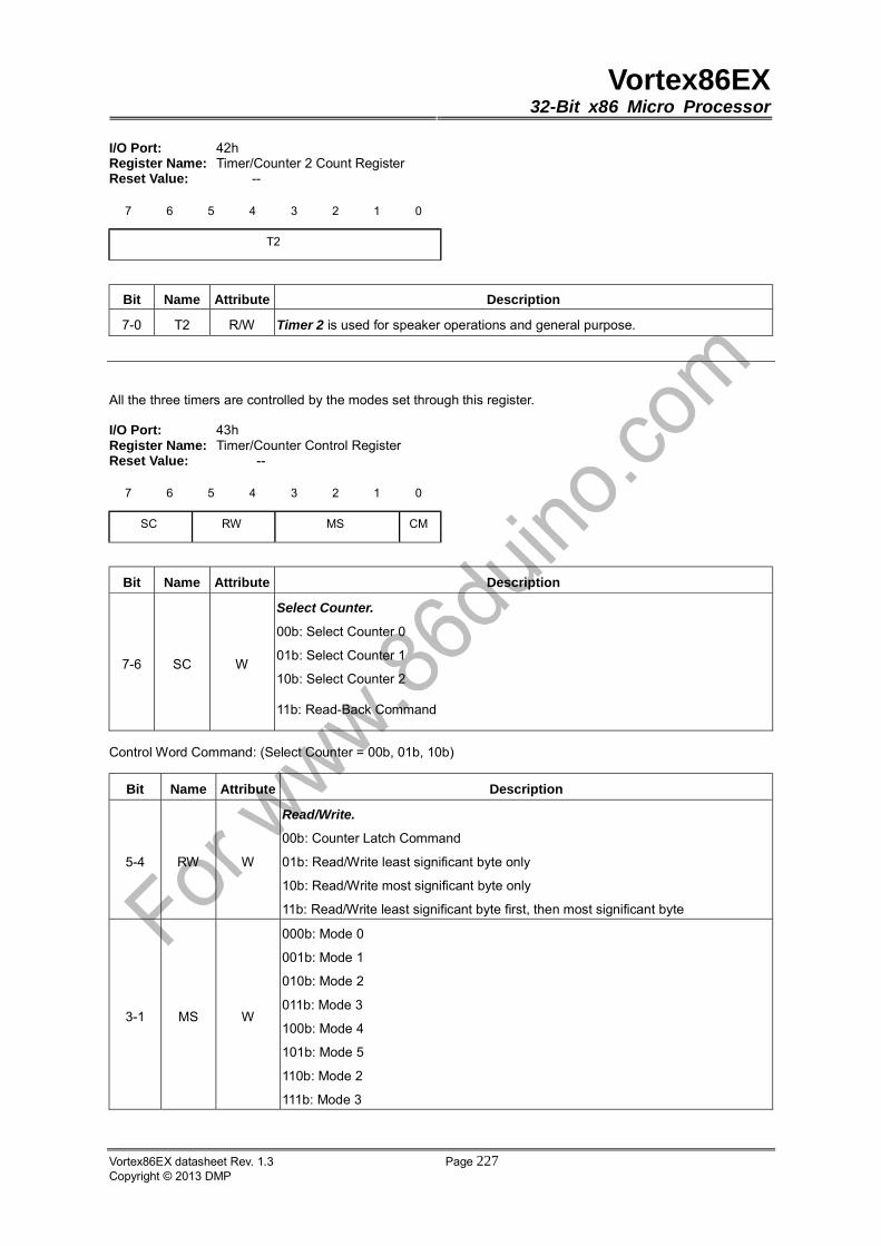
Vortex86EX32-Bit x86 Micro Processor
Vortex86EX datasheet Rev. 1.3 Page 227Copyright © 2013 DMP
I/O Port: 42h Register Name: Timer/Counter 2 Count Register Reset Value: --
7 6 5 4 3 2 1 0
T2
Bit Name Attribute Description
7-0 T2 R/W Timer 2 is used for speaker operations and general purpose.
All the three timers are controlled by the modes set through this register.
I/O Port: 43h Register Name: Timer/Counter Control Register Reset Value: --
7 6 5 4 3 2 1 0
SC RW MS CM
Bit Name Attribute Description
7-6 SC W
Select Counter.
00b: Select Counter 0
01b: Select Counter 1
10b: Select Counter 2
11b: Read-Back Command
Control Word Command: (Select Counter = 00b, 01b, 10b)
Bit Name Attribute Description
5-4 RW W
Read/Write.
00b: Counter Latch Command
01b: Read/Write least significant byte only
10b: Read/Write most significant byte only
11b: Read/Write least significant byte first, then most significant byte
3-1 MS W
000b: Mode 0
001b: Mode 1
010b: Mode 2
011b: Mode 3
100b: Mode 4
101b: Mode 5
110b: Mode 2
111b: Mode 3

Vortex86EX32-Bit x86 Micro Processor
Vortex86EX datasheet Rev. 1.3 Page 228Copyright © 2013 DMP
Bit Name Attribute Description
0 CM W 0b: Binary Counter mode (16-bit)
1b: BCD Counter mode (4 Binary Coded Decimal digits)
Counter Latch Command
SC1, SC0 – Specify counter to be latched
RW0, RW1 – 00 designates Counter Latch Command
D7 D6 D5 D4 D3 D2 D1 D0
SC1 SC0 0 0 X X X X
SC1 SC0 Counter
0 0 0
0 1 1
1 0 2
1 1 Read-Back Command
Read-back command: (Select Counter = 11b)
Bit Name Attribute Description
5-4 command W
Select command.
00b: Read-back status of selected counter(s) first, then count of selected
counter(s)
01b: Read-back count of selected counter(s)
10b: Read-back status of selected counter(s)
11b: X
3-1 counter W
Select counter.
001b: Select counter 1
001b: X
010b: Select counter 2
011b: X
100b: Select counter 3
101b: X
110b: X
111b: X
0 RSVD W Must be 0
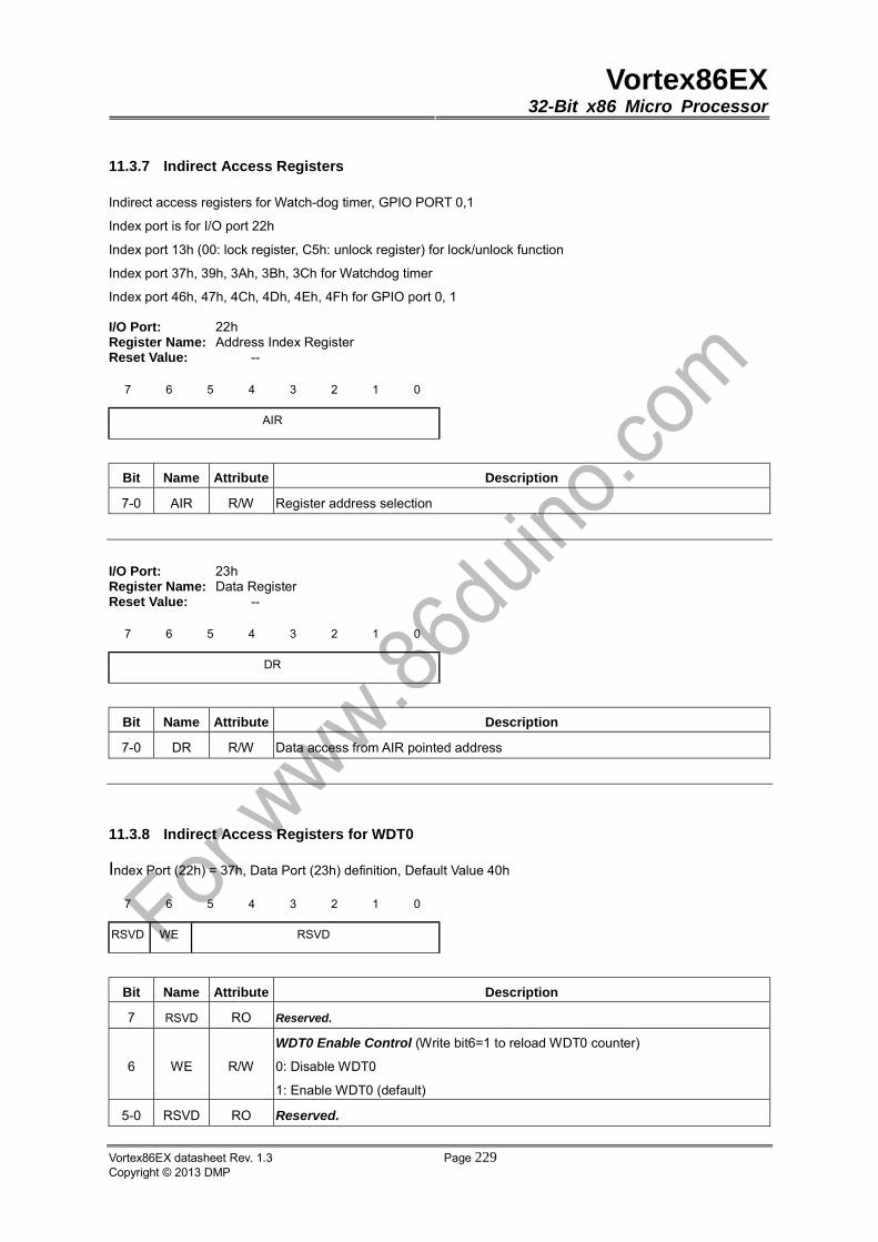
Vortex86EX32-Bit x86 Micro Processor
Vortex86EX datasheet Rev. 1.3 Page 229Copyright © 2013 DMP
11.3.7 Indirect Access Registers
Indirect access registers for Watch-dog timer, GPIO PORT 0,1
Index port is for I/O port 22h
Index port 13h (00: lock register, C5h: unlock register) for lock/unlock function
Index port 37h, 39h, 3Ah, 3Bh, 3Ch for Watchdog timer
Index port 46h, 47h, 4Ch, 4Dh, 4Eh, 4Fh for GPIO port 0, 1
I/O Port: 22h Register Name: Address Index Register Reset Value: --
7 6 5 4 3 2 1 0
AIR
Bit Name Attribute Description
7-0 AIR R/W Register address selection
I/O Port: 23h Register Name: Data Register Reset Value: --
7 6 5 4 3 2 1 0
DR
Bit Name Attribute Description
7-0 DR R/W Data access from AIR pointed address
11.3.8 Indirect Access Registers for WDT0
Index Port (22h) = 37h, Data Port (23h) definition, Default Value 40h
7 6 5 4 3 2 1 0
RSVD WE RSVD
Bit Name Attribute Description
7 RSVD RO Reserved.
6 WE R/W
WDT0 Enable Control (Write bit6=1 to reload WDT0 counter)
0: Disable WDT0
1: Enable WDT0 (default)
5-0 RSVD RO Reserved.
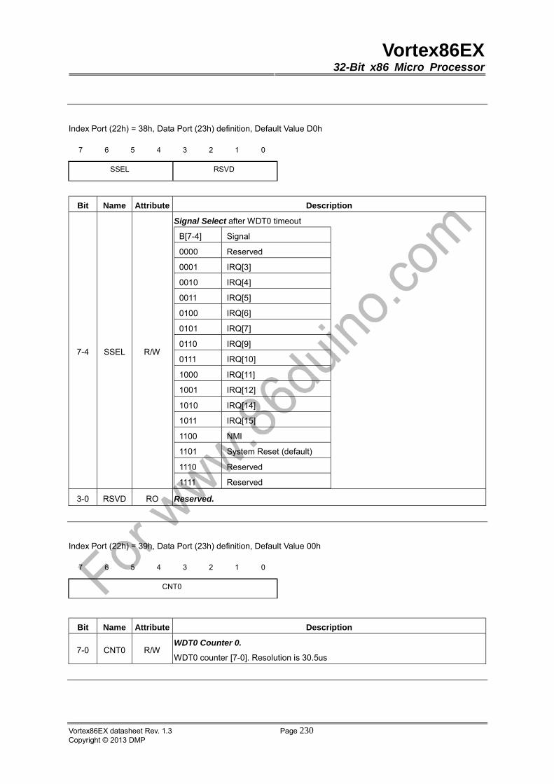
Vortex86EX32-Bit x86 Micro Processor
Vortex86EX datasheet Rev. 1.3 Page 230Copyright © 2013 DMP
Index Port (22h) = 38h, Data Port (23h) definition, Default Value D0h
7 6 5 4 3 2 1 0
SSEL RSVD
Bit Name Attribute Description
7-4 SSEL R/W
Signal Select after WDT0 timeout
B[7-4] Signal
0000 Reserved
0001 IRQ[3]
0010 IRQ[4]
0011 IRQ[5]
0100 IRQ[6]
0101 IRQ[7]
0110 IRQ[9]
0111 IRQ[10]
1000 IRQ[11]
1001 IRQ[12]
1010 IRQ[14]
1011 IRQ[15]
1100 NMI
1101 System Reset (default)
1110 Reserved
1111 Reserved
3-0 RSVD RO Reserved.
Index Port (22h) = 39h, Data Port (23h) definition, Default Value 00h
7 6 5 4 3 2 1 0
CNT0
Bit Name Attribute Description
7-0 CNT0 R/W WDT0 Counter 0.
WDT0 counter [7-0]. Resolution is 30.5us
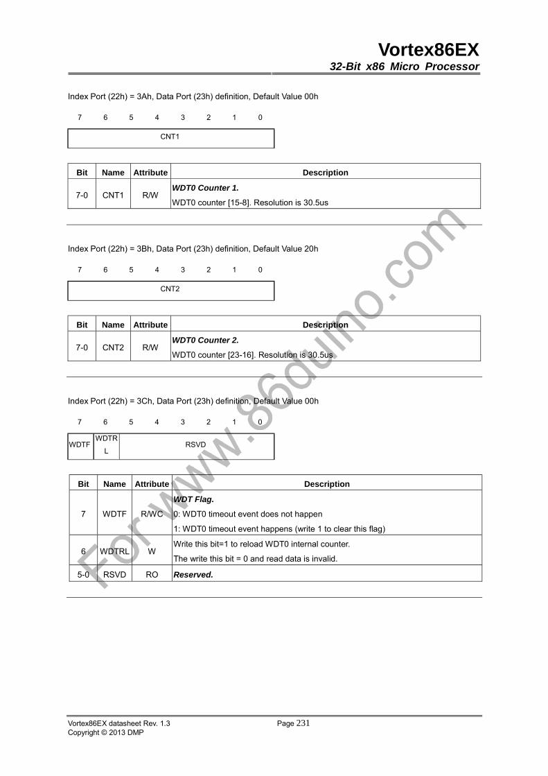
Vortex86EX32-Bit x86 Micro Processor
Vortex86EX datasheet Rev. 1.3 Page 231Copyright © 2013 DMP
Index Port (22h) = 3Ah, Data Port (23h) definition, Default Value 00h
7 6 5 4 3 2 1 0
CNT1
Bit Name Attribute Description
7-0 CNT1 R/W WDT0 Counter 1.
WDT0 counter [15-8]. Resolution is 30.5us
Index Port (22h) = 3Bh, Data Port (23h) definition, Default Value 20h
7 6 5 4 3 2 1 0
CNT2
Bit Name Attribute Description
7-0 CNT2 R/W WDT0 Counter 2.
WDT0 counter [23-16]. Resolution is 30.5us
Index Port (22h) = 3Ch, Data Port (23h) definition, Default Value 00h
7 6 5 4 3 2 1 0
WDTFWDTR
L RSVD
Bit Name Attribute Description
7 WDTF R/WC
WDT Flag.
0: WDT0 timeout event does not happen
1: WDT0 timeout event happens (write 1 to clear this flag)
6 WDTRL W Write this bit=1 to reload WDT0 internal counter.
The write this bit = 0 and read data is invalid.
5-0 RSVD RO Reserved.
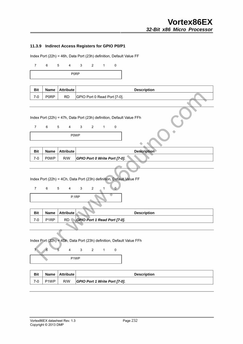
Vortex86EX32-Bit x86 Micro Processor
Vortex86EX datasheet Rev. 1.3 Page 232Copyright © 2013 DMP
11.3.9 Indirect Access Registers for GPIO P0/P1
Index Port (22h) = 46h, Data Port (23h) definition, Default Value FF
7 6 5 4 3 2 1 0
P0RP
Bit Name Attribute Description
7-0 P0RP RD GPIO Port 0 Read Port [7-0].
Index Port (22h) = 47h, Data Port (23h) definition, Default Value FFh
7 6 5 4 3 2 1 0
P0WP
Bit Name Attribute Description
7-0 P0WP R/W GPIO Port 0 Write Port [7-0].
Index Port (22h) = 4Ch, Data Port (23h) definition, Default Value FF
7 6 5 4 3 2 1 0
P.1RP
Bit Name Attribute Description
7-0 P1RP RD GPIO Port 1 Read Port [7-0].
Index Port (22h) = 4Dh, Data Port (23h) definition, Default Value FFh
7 6 5 4 3 2 1 0
P1WP
Bit Name Attribute Description
7-0 P1WP R/W GPIO Port 1 Write Port [7-0].

Vortex86EX32-Bit x86 Micro Processor
Vortex86EX datasheet Rev. 1.3 Page 233Copyright © 2013 DMP
Index Port (22h) = 4Eh, Data Port (23h) definition, Default Value 00h
7 6 5 4 3 2 1 0
P0DIR
Bit Name Attribute Description
7-0 P0DIR R/W
GPIO Port 0 Direction.
0: GPIO pin is input mode
1: GPIO pin is output mode
Index Port (22h) = 4Fh, Data Port (23h) definition, Default Value 00h
7 6 5 4 3 2 1 0
P1DIR
Bit Name Attribute Description
7-0 P1DIR R/W
GPIO Port 1 Direction.
0: GPIO pin is input mode
1: GPIO pin is output mode
11.3.10 Indirect Access Registers for Lock / Unlock
Index Port (22h) = 13h, Data Port (23h) = C5h; Unlock function, Port 22h/23h for GPIO/WDT0 works
Index Port (22h) = 13h, Data Port (23h) = 00h ; Lock GPIO/WDT0 function
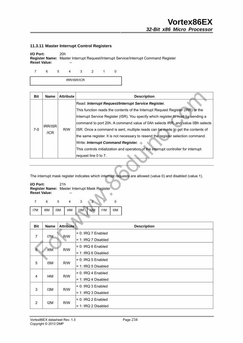
Vortex86EX32-Bit x86 Micro Processor
Vortex86EX datasheet Rev. 1.3 Page 234Copyright © 2013 DMP
11.3.11 Master Interrupt Control Registers
I/O Port: 20h Register Name: Master Interrupt Request/Interrupt Service/Interrupt Command Register Reset Value: --
7 6 5 4 3 2 1 0
IRR/ISR/ICR
Bit Name Attribute Description
7-0IRR/ISR
/ICR R/W
Read: Interrupt Request/Interrupt Service Register.
This function reads the contents of the Interrupt Request Register (IRR) or the
Interrupt Service Register (ISR). You specify which register to read by sending a
command to port 20h. A command value of 0Ah selects IRR, and value 0Bh selects
ISR. Once a command is sent, multiple reads can be made to get the contents of
the same register. It is not necessary to resend the register selection command.
Write: Interrupt Command Register.
This controls initialization and operation of the interrupt controller for interrupt
request line 0 to 7.
The interrupt mask register indicates which interrupt requests are allowed (value 0) and disabled (value 1).
I/O Port: 21h Register Name: Master Interrupt Mask Register Reset Value: --
7 6 5 4 3 2 1 0
I7M I6M I5M I4M I3M I2M I1M I0M
Bit Name Attribute Description
7 I7M R/W = 0: IRQ 7 Enabled
= 1: IRQ 7 Disabled
6 I6M R/W = 0: IRQ 6 Enabled
= 1: IRQ 6 Disabled
5 I5M R/W = 0: IRQ 5 Enabled
= 1: IRQ 5 Disabled
4 I4M R/W = 0: IRQ 4 Enabled
= 1: IRQ 4 Disabled
3 I3M R/W = 0: IRQ 3 Enabled
= 1: IRQ 3 Disabled
2 I2M R/W = 0: IRQ 2 Enabled
= 1: IRQ 2 Disabled

Vortex86EX32-Bit x86 Micro Processor
Vortex86EX datasheet Rev. 1.3 Page 235Copyright © 2013 DMP
Bit Name Attribute Description
1 I1M R/W = 0: IRQ 1 Enabled
= 1: IRQ 1 Disabled
0 I0M R/W = 0: IRQ 0 Enabled
= 1: IRQ 0 Disabled
11.3.12 Slave Interrupt Control Registers
I/O Port: A0h Register Name: Slave Interrupt Request/Interrupt Service/Interrupt Command Register Reset Value: --
7 6 5 4 3 2 1 0
IRR/ISR/ICR
Bit Name Attribute Description
7-0IRR/IS
R/ICRR/W
Read: Interrupt Request/Interrupt Service Register.
This function reads the contents of the Interrupt Request Register (IRR) or the
Interrupt Service Register (ISR). You specify which register to read by sending a
command to port A0h. A command value of 0Ah selects IRR, and value 0Bh selects
ISR. Once a command is sent, multiple reads can be made to get the contents of
the same register. It is not necessary to resend the register selection command.
Write: Interrupt Command Register.
This controls initialization and operation of the interrupt controller for interrupt
request line 8 to 15.
The interrupt mask register indicates which interrupt requests are allowed (value 0) and which are disabled
(value 1).
I/O Port: A1h Register Name: Slave Interrupt Mask Register Reset Value: --
7 6 5 4 3 2 1 0
I15M I14M I13M I12M I11M I10M I9M I8M
Bit Name Attribute Description
7 I15M R/W = 0: IRQ 15 Enabled
= 1: IRQ 15 Disabled
6 I14M R/W = 0: IRQ 14 Enabled
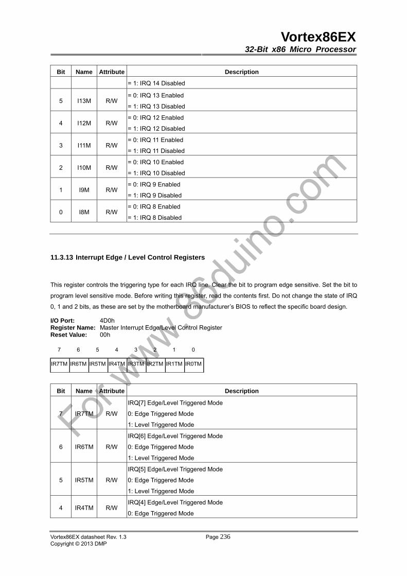
Vortex86EX32-Bit x86 Micro Processor
Vortex86EX datasheet Rev. 1.3 Page 236Copyright © 2013 DMP
Bit Name Attribute Description
= 1: IRQ 14 Disabled
5 I13M R/W = 0: IRQ 13 Enabled
= 1: IRQ 13 Disabled
4 I12M R/W = 0: IRQ 12 Enabled
= 1: IRQ 12 Disabled
3 I11M R/W = 0: IRQ 11 Enabled
= 1: IRQ 11 Disabled
2 I10M R/W = 0: IRQ 10 Enabled
= 1: IRQ 10 Disabled
1 I9M R/W = 0: IRQ 9 Enabled
= 1: IRQ 9 Disabled
0 I8M R/W = 0: IRQ 8 Enabled
= 1: IRQ 8 Disabled
11.3.13 Interrupt Edge / Level Control Registers
This register controls the triggering type for each IRQ line. Clear the bit to program edge sensitive. Set the bit to
program level sensitive mode. Before writing this register, read the contents first. Do not change the state of IRQ
0, 1 and 2 bits, as these are set by the motherboard manufacturer’s BIOS to reflect the specific board design.
I/O Port: 4D0h Register Name: Master Interrupt Edge/Level Control Register Reset Value: 00h
7 6 5 4 3 2 1 0
IR7TM IR6TM IR5TM IR4TM IR3TM IR2TM IR1TM IR0TM
Bit Name Attribute Description
7 IR7TM R/W
IRQ[7] Edge/Level Triggered Mode
0: Edge Triggered Mode
1: Level Triggered Mode
6 IR6TM R/W
IRQ[6] Edge/Level Triggered Mode
0: Edge Triggered Mode
1: Level Triggered Mode
5 IR5TM R/W
IRQ[5] Edge/Level Triggered Mode
0: Edge Triggered Mode
1: Level Triggered Mode
4 IR4TM R/W IRQ[4] Edge/Level Triggered Mode
0: Edge Triggered Mode
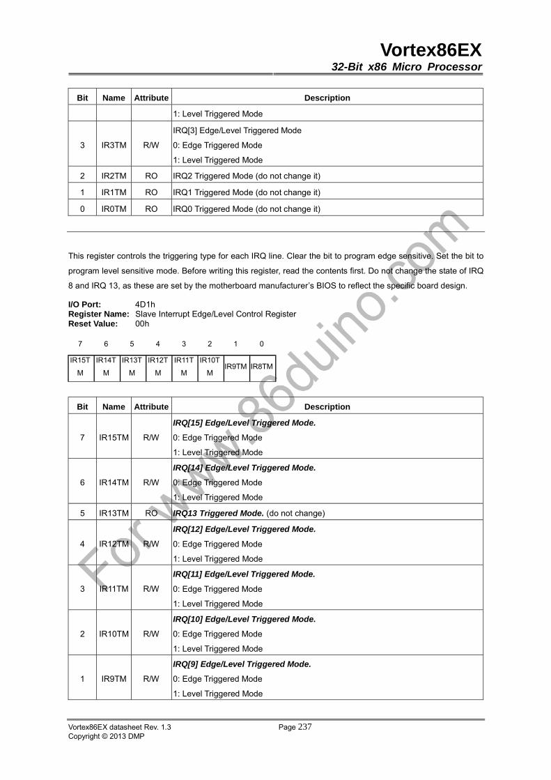
Vortex86EX32-Bit x86 Micro Processor
Vortex86EX datasheet Rev. 1.3 Page 237Copyright © 2013 DMP
Bit Name Attribute Description
1: Level Triggered Mode
3 IR3TM R/W
IRQ[3] Edge/Level Triggered Mode
0: Edge Triggered Mode
1: Level Triggered Mode
2 IR2TM RO IRQ2 Triggered Mode (do not change it)
1 IR1TM RO IRQ1 Triggered Mode (do not change it)
0 IR0TM RO IRQ0 Triggered Mode (do not change it)
This register controls the triggering type for each IRQ line. Clear the bit to program edge sensitive. Set the bit to
program level sensitive mode. Before writing this register, read the contents first. Do not change the state of IRQ
8 and IRQ 13, as these are set by the motherboard manufacturer’s BIOS to reflect the specific board design.
I/O Port: 4D1h Register Name: Slave Interrupt Edge/Level Control Register Reset Value: 00h
7 6 5 4 3 2 1 0
IR15T
M
IR14T
M
IR13T
M
IR12T
M
IR11T
M
IR10T
M IR9TM IR8TM
Bit Name Attribute Description
7 IR15TM R/W
IRQ[15] Edge/Level Triggered Mode.
0: Edge Triggered Mode
1: Level Triggered Mode
6 IR14TM R/W
IRQ[14] Edge/Level Triggered Mode.
0: Edge Triggered Mode
1: Level Triggered Mode
5 IR13TM RO IRQ13 Triggered Mode. (do not change)
4 IR12TM R/W
IRQ[12] Edge/Level Triggered Mode.
0: Edge Triggered Mode
1: Level Triggered Mode
3 IR11TM R/W
IRQ[11] Edge/Level Triggered Mode.
0: Edge Triggered Mode
1: Level Triggered Mode
2 IR10TM R/W
IRQ[10] Edge/Level Triggered Mode.
0: Edge Triggered Mode
1: Level Triggered Mode
1 IR9TM R/W
IRQ[9] Edge/Level Triggered Mode.
0: Edge Triggered Mode
1: Level Triggered Mode
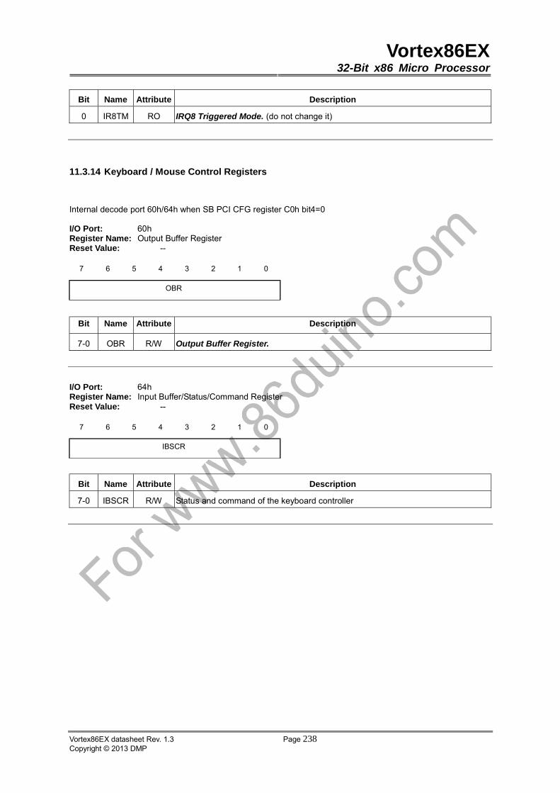
Vortex86EX32-Bit x86 Micro Processor
Vortex86EX datasheet Rev. 1.3 Page 238Copyright © 2013 DMP
Bit Name Attribute Description
0 IR8TM RO IRQ8 Triggered Mode. (do not change it)
11.3.14 Keyboard / Mouse Control Registers
Internal decode port 60h/64h when SB PCI CFG register C0h bit4=0
I/O Port: 60h Register Name: Output Buffer Register Reset Value: --
7 6 5 4 3 2 1 0
OBR
Bit Name Attribute Description
7-0 OBR R/W Output Buffer Register.
I/O Port: 64h Register Name: Input Buffer/Status/Command Register Reset Value: --
7 6 5 4 3 2 1 0
IBSCR
Bit Name Attribute Description
7-0 IBSCR R/W Status and command of the keyboard controller
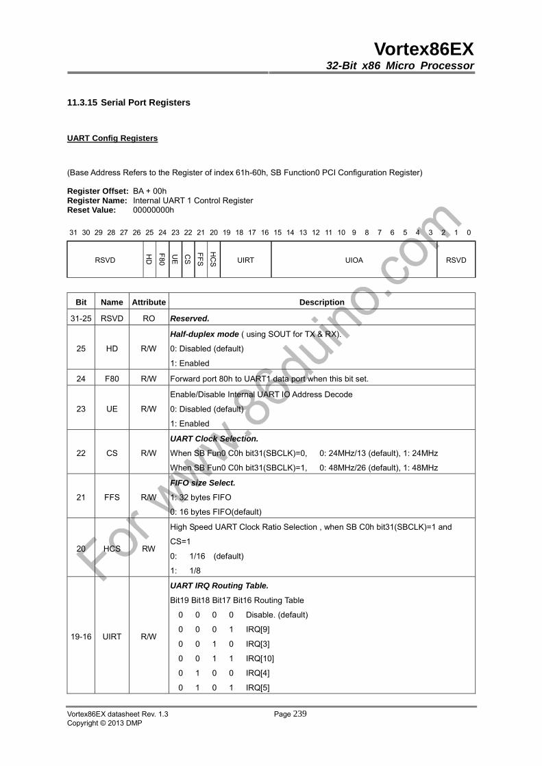
Vortex86EX32-Bit x86 Micro Processor
Vortex86EX datasheet Rev. 1.3 Page 239Copyright © 2013 DMP
11.3.15 Serial Port Registers
UART Config Registers
(Base Address Refers to the Register of index 61h-60h, SB Function0 PCI Configuration Register)
Register Offset: BA + 00h Register Name: Internal UART 1 Control Register Reset Value: 00000000h
31 30 29 28 27 26 25 24 23 22 21 20 19 18 17 16 15 14 13 12 11 10 9 8 7 6 5 4 3 2 1 0
RSVD UIRT UIOA RSVD
Bit Name Attribute Description
31-25 RSVD RO Reserved.
25 HD R/W
Half-duplex mode ( using SOUT for TX & RX).
0: Disabled (default)
1: Enabled
24 F80 R/W Forward port 80h to UART1 data port when this bit set.
23 UE R/W
Enable/Disable Internal UART IO Address Decode
0: Disabled (default)
1: Enabled
22 CS R/W
UART Clock Selection.
When SB Fun0 C0h bit31(SBCLK)=0, 0: 24MHz/13 (default), 1: 24MHz
When SB Fun0 C0h bit31(SBCLK)=1, 0: 48MHz/26 (default), 1: 48MHz
21 FFS R/W
FIFO size Select.
1: 32 bytes FIFO
0: 16 bytes FIFO(default)
20 HCS RW
High Speed UART Clock Ratio Selection , when SB C0h bit31(SBCLK)=1 and
CS=1
0: 1/16 (default)
1: 1/8
19-16 UIRT R/W
UART IRQ Routing Table.
Bit19 Bit18 Bit17 Bit16 Routing Table
0 0 0 0 Disable. (default)
0 0 0 1 IRQ[9]
0 0 1 0 IRQ[3]
0 0 1 1 IRQ[10]
0 1 0 0 IRQ[4]
0 1 0 1 IRQ[5]
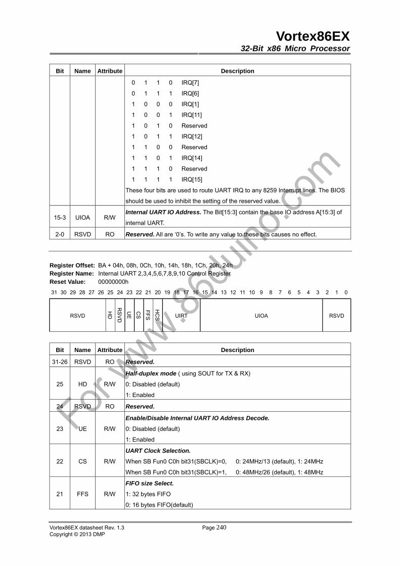
Vortex86EX32-Bit x86 Micro Processor
Vortex86EX datasheet Rev. 1.3 Page 240Copyright © 2013 DMP
Bit Name Attribute Description
0 1 1 0 IRQ[7]
0 1 1 1 IRQ[6]
1 0 0 0 IRQ[1]
1 0 0 1 IRQ[11]
1 0 1 0 Reserved
1 0 1 1 IRQ[12]
1 1 0 0 Reserved
1 1 0 1 IRQ[14]
1 1 1 0 Reserved
1 1 1 1 IRQ[15]
These four bits are used to route UART IRQ to any 8259 Interrupt lines. The BIOS
should be used to inhibit the setting of the reserved value.
15-3 UIOA R/W Internal UART IO Address. The Bit[15:3] contain the base IO address A[15:3] of
internal UART.
2-0 RSVD RO Reserved. All are ‘0’s. To write any value to these bits causes no effect.
Register Offset: BA + 04h, 08h, 0Ch, 10h, 14h, 18h, 1Ch, 20h, 24h Register Name: Internal UART 2,3,4,5,6,7,8,9,10 Control Register Reset Value: 00000000h
31 30 29 28 27 26 25 24 23 22 21 20 19 18 17 16 15 14 13 12 11 10 9 8 7 6 5 4 3 2 1 0
RSVD UIRT UIOA RSVD
Bit Name Attribute Description
31-26 RSVD RO Reserved.
25 HD R/W
Half-duplex mode ( using SOUT for TX & RX)
0: Disabled (default)
1: Enabled
24 RSVD RO Reserved.
23 UE R/W
Enable/Disable Internal UART IO Address Decode.
0: Disabled (default)
1: Enabled
22 CS R/W
UART Clock Selection.
When SB Fun0 C0h bit31(SBCLK)=0, 0: 24MHz/13 (default), 1: 24MHz
When SB Fun0 C0h bit31(SBCLK)=1, 0: 48MHz/26 (default), 1: 48MHz
21 FFS R/W
FIFO size Select.
1: 32 bytes FIFO
0: 16 bytes FIFO(default)
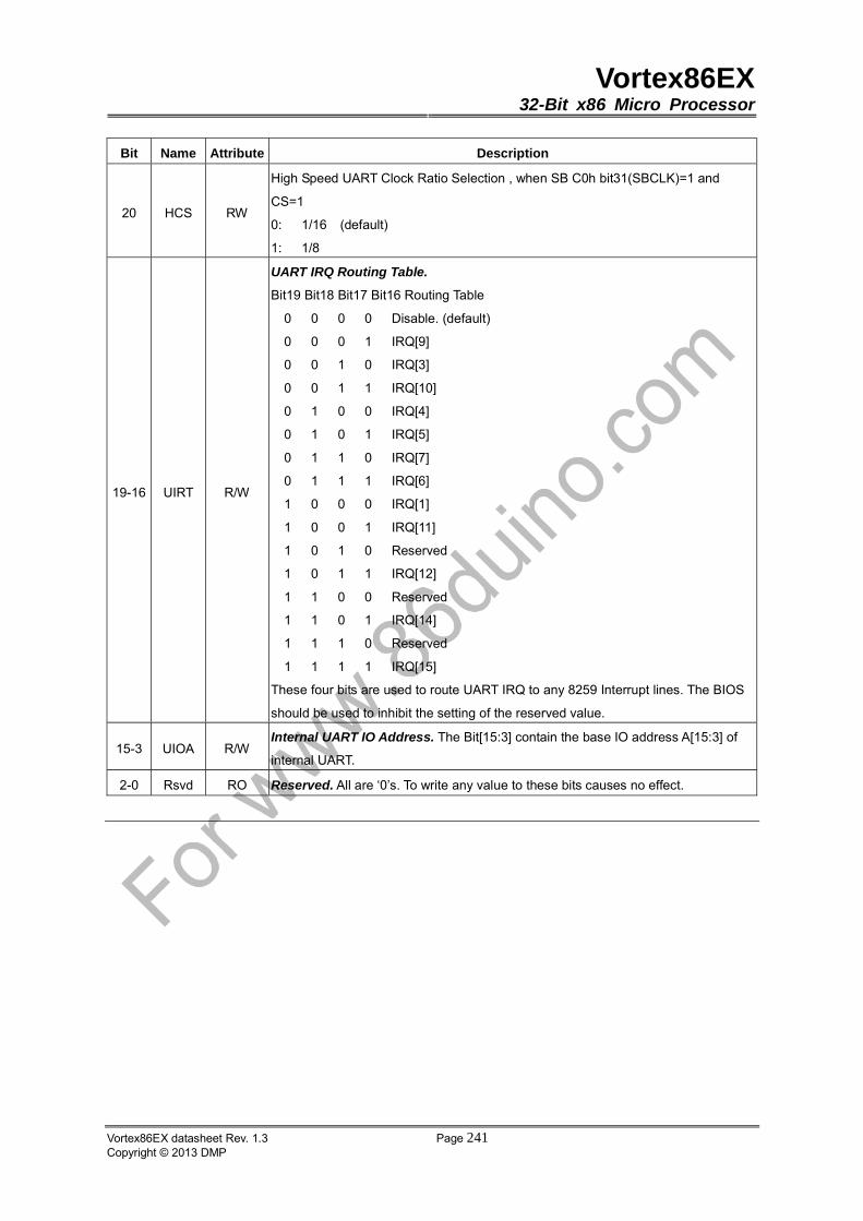
Vortex86EX32-Bit x86 Micro Processor
Vortex86EX datasheet Rev. 1.3 Page 241Copyright © 2013 DMP
Bit Name Attribute Description
20 HCS RW
High Speed UART Clock Ratio Selection , when SB C0h bit31(SBCLK)=1 and
CS=1
0: 1/16 (default)
1: 1/8
19-16 UIRT R/W
UART IRQ Routing Table.
Bit19 Bit18 Bit17 Bit16 Routing Table
0 0 0 0 Disable. (default)
0 0 0 1 IRQ[9]
0 0 1 0 IRQ[3]
0 0 1 1 IRQ[10]
0 1 0 0 IRQ[4]
0 1 0 1 IRQ[5]
0 1 1 0 IRQ[7]
0 1 1 1 IRQ[6]
1 0 0 0 IRQ[1]
1 0 0 1 IRQ[11]
1 0 1 0 Reserved
1 0 1 1 IRQ[12]
1 1 0 0 Reserved
1 1 0 1 IRQ[14]
1 1 1 0 Reserved
1 1 1 1 IRQ[15]
These four bits are used to route UART IRQ to any 8259 Interrupt lines. The BIOS
should be used to inhibit the setting of the reserved value.
15-3 UIOA R/W Internal UART IO Address. The Bit[15:3] contain the base IO address A[15:3] of
internal UART.
2-0 Rsvd RO Reserved. All are ‘0’s. To write any value to these bits causes no effect.
Vortex86EX32-Bit x86 Micro Processor
Vortex86EX datasheet Rev. 1.3 Page 242Copyright © 2013 DMP
Serial Port Registers
The system programmer may access any of the UART registers. These registers control UART operations
including transmission and reception of data.
(UART1 Base Address Refers to UART Config Register Offset 00h )
(UART2 Base Address Refers to UART Config Register Offset 04h)
(UART3 Base Address Refers to UART Config Register Offset 08h)
(UART4 Base Address Refers to UART Config Register Offset 0Ch)
(UART5 Base Address Refers to UART Config Register Offset 10h)
(UART6 Base Address Refers to UART Config Register Offset 14h)
(UART7 Base Address Refers to UART Config Register Offset 18h)
(UART8 Base Address Refers to UART Config Register Offset 1Ch)
(UART9 Base Address Refers to UART Config Register Offset 20h)
(UART10 Base Address Refers to UART Config Register Offset 24h)
An output to this register stores a byte into the UART’s transmit holding buffer. An input gets a byte from the
receive buffer of the UART. These are two separate registers within the UART. To access this register, the
Divisor Latch Access Bit (DLAB) must be zero. DLAB is bit 7 in the line control register 3.
I/O Port: Base Address + 0h Register Name: Transmit/Receive Data Buffer (DLAB=0) Reset Value: --
7 6 5 4 3 2 1 0
TD/RD
Bit Name Attribute Description
7-0 TD/RD R/W Read: This register holds the received incoming data byte.
Write: This register contains the data byte to be transmitted.

Vortex86EX32-Bit x86 Micro Processor
Vortex86EX datasheet Rev. 1.3 Page 243Copyright © 2013 DMP
The UART contains a programmable baud generator that is capable of taking any clock input from DC to 24 MHz
and dividing it by any divisor from 2 to 216-1. The output frequency of the baud generator is 16 X the baud
[divisor # = (frequency input) / (baud rate X 16)]. Two 8-bit latches store the divisor in a 16-bit binary format.
These divisor latches must be loaded during initialization to ensure proper operation of the baud generator. Upon
loading either of the divisor latches, a 16-bit baud counter is immediately loaded. The Table listed below provides
decimal divisors to use with crystal frequencies of 1.8432 MHz and 24 MHz, respectively. For baud rates of
38400 and below, the error obtained is minimal. The accuracy of the desired baud rate is dependent on the
crystal frequency chosen. Using a divisor of zero is not recommended.
I/O Port: Base Address + 0h Register Name: LSB of Baud Rate Generator Divisor Latches (DLAB=1) Reset Value: 01h
7 6 5 4 3 2 1 0
LBR
Bit Name Attribute Description
7-0 LBR R/W This register contains the LSB (Least Significant Byte) of divisor latches.
TABLE Baud Rates, Divisors and 1.8432MHzCrystals
Baud Rate Decimal Divisor
for 16 X Clock Percent Error
50
75
110
134.5
150
300
600
1200
1800
2000
2400
3600
4800
7200
9600
19200
38400
57600
115200
2304
1536
1047
857
768
384
192
96
64
58
48
32
24
16
12
6
3
2
1
-
-
0.026
0.058
-
-
-
-
-
0.69
-
-
-
-
-
-
-
2.68
-
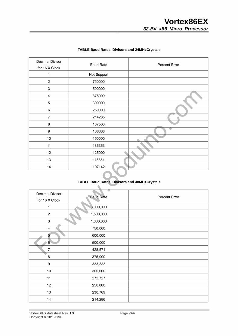
Vortex86EX32-Bit x86 Micro Processor
Vortex86EX datasheet Rev. 1.3 Page 244Copyright © 2013 DMP
TABLE Baud Rates, Divisors and 24MHzCrystals
Decimal Divisor
for 16 X Clock Baud Rate Percent Error
1 Not Support
2 750000
3 500000
4 375000
5 300000
6 250000
7 214285
8 187500
9 166666
10 150000
11 136363
12 125000
13 115384
14 107142
TABLE Baud Rates, Divisors and 48MHzCrystals
Decimal Divisor
for 16 X Clock Baud Rate Percent Error
1 3,000,000
2 1,500,000
3 1,000,000
4 750,000
5 600,000
6 500,000
7 428,571
8 375,000
9 333,333
10 300,000
11 272,727
12 250,000
13 230,769
14 214,286
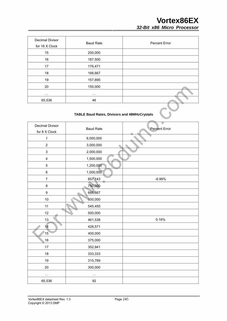
Vortex86EX32-Bit x86 Micro Processor
Vortex86EX datasheet Rev. 1.3 Page 245Copyright © 2013 DMP
Decimal Divisor
for 16 X Clock Baud Rate Percent Error
15 200,000
16 187,500
17 176,471
18 166,667
19 157,895
20 150,000
… …
65,536 46
TABLE Baud Rates, Divisors and 48MHzCrystals
Decimal Divisor
for 8 X Clock Baud Rate Percent Error
1 6,000,000
2 3,000,000
3 2,000,000
4 1,500,000
5 1,200,000
6 1,000,000
7 857,143 -6.99%
8 750,000
9 666,667
10 600,000
11 545,455
12 500,000
13 461,538 0.16%
14 428,571
15 400,000
16 375,000
17 352,941
18 333,333
19 315,789
20 300,000
… …
65,536 92

Vortex86EX32-Bit x86 Micro Processor
Vortex86EX datasheet Rev. 1.3 Page 246Copyright © 2013 DMP
This register enables the five types of UART interrupts. Each interrupt can individually activate the interrupt
(INTR) output signal. It is possible to totally disable the interrupt system by resetting bit 0 through 3 of the
Interrupt Enable Register (IER). Similarly, setting bits of the IER register to a logic 1 enables the selected
interrupt(s). Disabling an interrupt prevents it from being indicated as active in the IIR and from activating the
INTR output signal. All other system functions operate in their normal manner, including the settings of the Line
Status and MODEM Status Registers. Table II shows the contents of the IER. Details on each bit are listed as
follows.
I/O Port: Base Address + 1h Register Name: Interrupt Enable Register (DLAB=0) Reset Value: 00h
7 6 5 4 3 2 1 0
RSVD MSI RLSI THREI RDAI
Bit Name Attribute Description
7-4 RSVD RO Reserved. Must be always ‘0’
3 MSI R/W
Modem Status Interrupt.
0: Disabled
1: Enabled
2 RLSI R/W
Received Line Status Interrupt.
0: Disabled
1: Enabled
1 THREI R/W
Transmitter Holding Register Empty Interrupt.
0: Disabled
1: Enabled
0 RDAI R/W
Received Data Available Interrupt.
0: Disabled
1: Enabled
I/O Port: Base Address + 1h Register Name: MSB of Baud Rate Generator Divisor Latches (DLAB=1) Reset Value: 00h
7 6 5 4 3 2 1 0
MBR
Bit Name Attribute Description
7-0 MBR R/W This register contains the MSB (Most Significant Byte) of divisor latches.
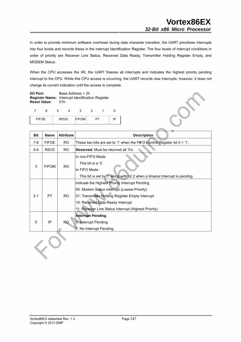
Vortex86EX32-Bit x86 Micro Processor
Vortex86EX datasheet Rev. 1.3 Page 247Copyright © 2013 DMP
In order to provide minimum software overhead during data character transfers, the UART prioritizes interrupts
into four levels and records these in the interrupt Identification Register. The four levels of interrupt conditions in
order of priority are Receiver Line Status, Received Data Ready, Transmitter Holding Register Empty, and
MODEM Status.
When the CPU accesses the IIR, the UART freezes all interrupts and indicates the highest priority pending
interrupt to the CPU. While this CPU access is occurring, the UART records new interrupts; however, it does not
change its current indication until the access is complete.
I/O Port: Base Address + 2h Register Name: Interrupt Identification Register Reset Value: 01h
7 6 5 4 3 2 1 0
FIFOE RSVD FIFOM PT IP
Bit Name Attribute Description
7-6 FIFOE RO These two bits are set to ‘1’ when the FIFO Control Register bit 0 = ‘1’.
5-4 RSVD RO Reserved. Must be returned all ‘0’s.
3 FIFOM RO
In non-FIFO Mode
This bit is a ‘0’.
In FIFO Mode
This bit is set to ‘1’ along with bit 2 when a timeout interrupt is pending
2-1 PT RO
Indicate the Highest Priority Interrupt Pending
00: Modem Status Interrupt (Lowest Priority)
01: Transmitter Holding Register Empty Interrupt
10: Received Data Ready Interrupt
11: Receiver Line Status Interrupt (Highest Priority)
0 IP RO
Interrupt Pending.
0: Interrupt Pending
1: No Interrupt Pending
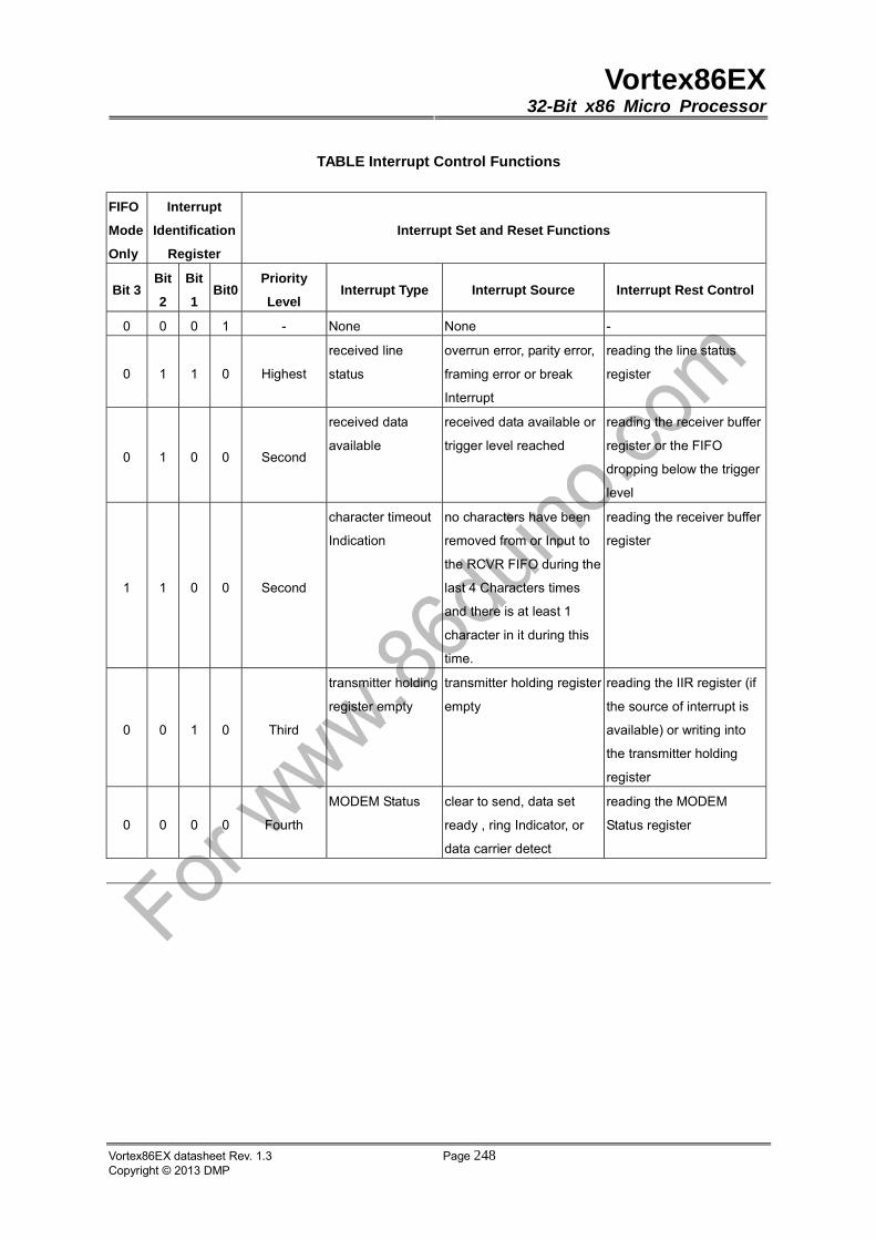
Vortex86EX32-Bit x86 Micro Processor
Vortex86EX datasheet Rev. 1.3 Page 248Copyright © 2013 DMP
TABLE Interrupt Control Functions
FIFO
Mode
Only
Interrupt
Identification
Register
Interrupt Set and Reset Functions
Bit 3Bit
2
Bit
1Bit0
Priority
Level Interrupt Type Interrupt Source Interrupt Rest Control
0 0 0 1 - None None -
0 1 1 0 Highest
received line
status
overrun error, parity error,
framing error or break
Interrupt
reading the line status
register
0 1 0 0 Second
received data
available
received data available or
trigger level reached
reading the receiver buffer
register or the FIFO
dropping below the trigger
level
1 1 0 0 Second
character timeout
Indication
no characters have been
removed from or Input to
the RCVR FIFO during the
last 4 Characters times
and there is at least 1
character in it during this
time.
reading the receiver buffer
register
0 0 1 0 Third
transmitter holding
register empty
transmitter holding register
empty
reading the IIR register (if
the source of interrupt is
available) or writing into
the transmitter holding
register
0 0 0 0 Fourth
MODEM Status clear to send, data set
ready , ring Indicator, or
data carrier detect
reading the MODEM
Status register
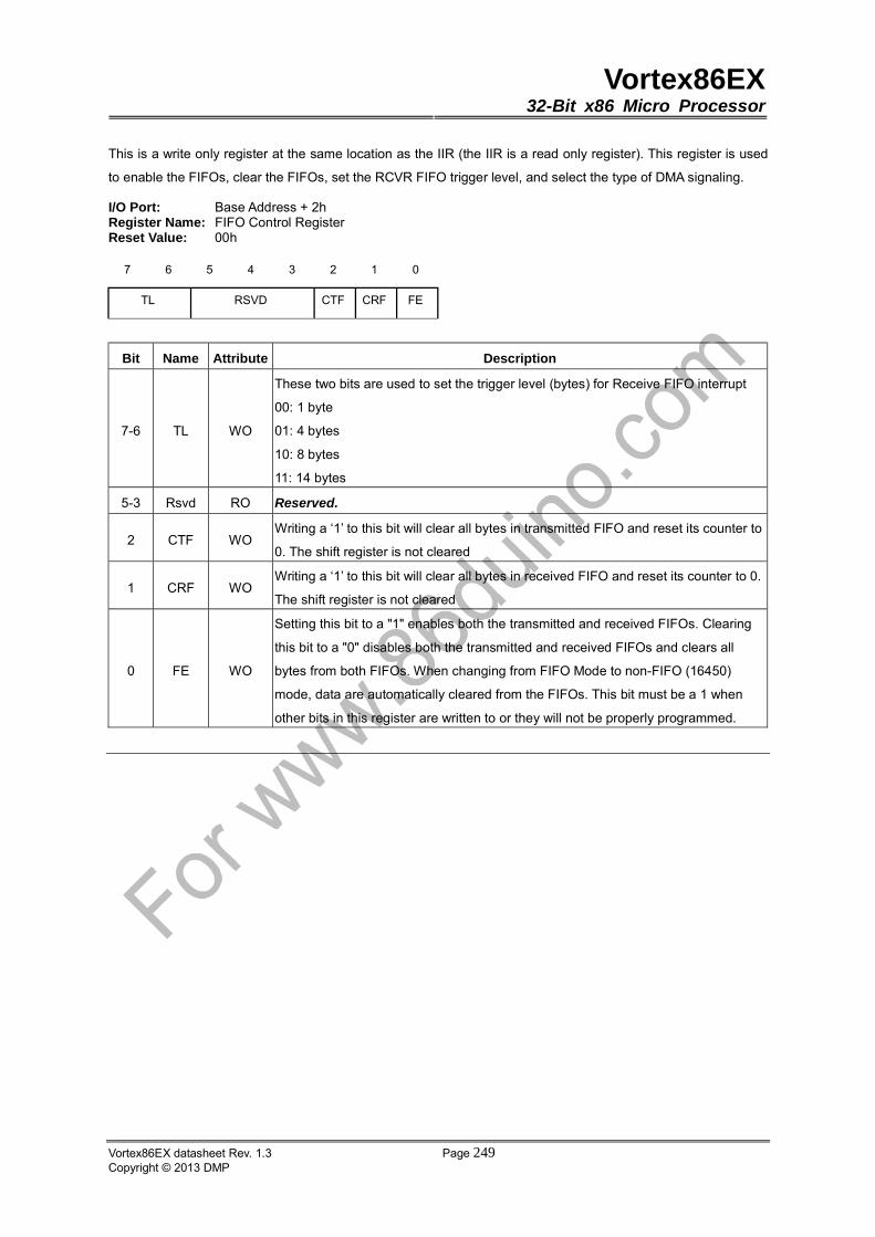
Vortex86EX32-Bit x86 Micro Processor
Vortex86EX datasheet Rev. 1.3 Page 249Copyright © 2013 DMP
This is a write only register at the same location as the IIR (the IIR is a read only register). This register is used
to enable the FIFOs, clear the FIFOs, set the RCVR FIFO trigger level, and select the type of DMA signaling.
I/O Port: Base Address + 2h Register Name: FIFO Control Register Reset Value: 00h
7 6 5 4 3 2 1 0
TL RSVD CTF CRF FE
Bit Name Attribute Description
7-6 TL WO
These two bits are used to set the trigger level (bytes) for Receive FIFO interrupt
00: 1 byte
01: 4 bytes
10: 8 bytes
11: 14 bytes
5-3 Rsvd RO Reserved.
2 CTF WO Writing a ‘1’ to this bit will clear all bytes in transmitted FIFO and reset its counter to
0. The shift register is not cleared
1 CRF WO Writing a ‘1’ to this bit will clear all bytes in received FIFO and reset its counter to 0.
The shift register is not cleared
0 FE WO
Setting this bit to a "1" enables both the transmitted and received FIFOs. Clearing
this bit to a "0" disables both the transmitted and received FIFOs and clears all
bytes from both FIFOs. When changing from FIFO Mode to non-FIFO (16450)
mode, data are automatically cleared from the FIFOs. This bit must be a 1 when
other bits in this register are written to or they will not be properly programmed.
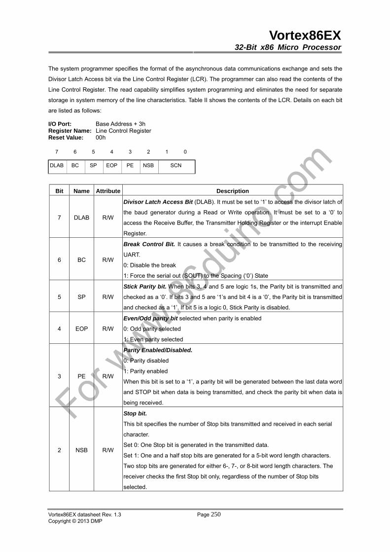
Vortex86EX32-Bit x86 Micro Processor
Vortex86EX datasheet Rev. 1.3 Page 250Copyright © 2013 DMP
The system programmer specifies the format of the asynchronous data communications exchange and sets the
Divisor Latch Access bit via the Line Control Register (LCR). The programmer can also read the contents of the
Line Control Register. The read capability simplifies system programming and eliminates the need for separate
storage in system memory of the line characteristics. Table II shows the contents of the LCR. Details on each bit
are listed as follows:
I/O Port: Base Address + 3h Register Name: Line Control Register Reset Value: 00h
7 6 5 4 3 2 1 0
DLAB BC SP EOP PE NSB SCN
Bit Name Attribute Description
7 DLAB R/W
Divisor Latch Access Bit (DLAB). It must be set to ‘1’ to access the divisor latch of
the baud generator during a Read or Write operation. It must be set to a ‘0’ to
access the Receive Buffer, the Transmitter Holding Register or the interrupt Enable
Register.
6 BC R/W
Break Control Bit. It causes a break condition to be transmitted to the receiving
UART.
0: Disable the break
1: Force the serial out (SOUT) to the Spacing (‘0’) State
5 SP R/W
Stick Parity bit. When bits 3, 4 and 5 are logic 1s, the Parity bit is transmitted and
checked as a ‘0’. If bits 3 and 5 are ‘1’s and bit 4 is a ‘0’, the Parity bit is transmitted
and checked as a ‘1’. If bit 5 is a logic 0, Stick Parity is disabled.
4 EOP R/W
Even/Odd parity bit selected when parity is enabled
0: Odd parity selected
1: Even parity selected
3 PE R/W
Parity Enabled/Disabled.
0: Parity disabled
1: Parity enabled
When this bit is set to a ‘1’, a parity bit will be generated between the last data word
and STOP bit when data is being transmitted, and check the parity bit when data is
being received.
2 NSB R/W
Stop bit.
This bit specifies the number of Stop bits transmitted and received in each serial
character.
Set 0: One Stop bit is generated in the transmitted data.
Set 1: One and a half stop bits are generated for a 5-bit word length characters.
Two stop bits are generated for either 6-, 7-, or 8-bit word length characters. The
receiver checks the first Stop bit only, regardless of the number of Stop bits
selected.
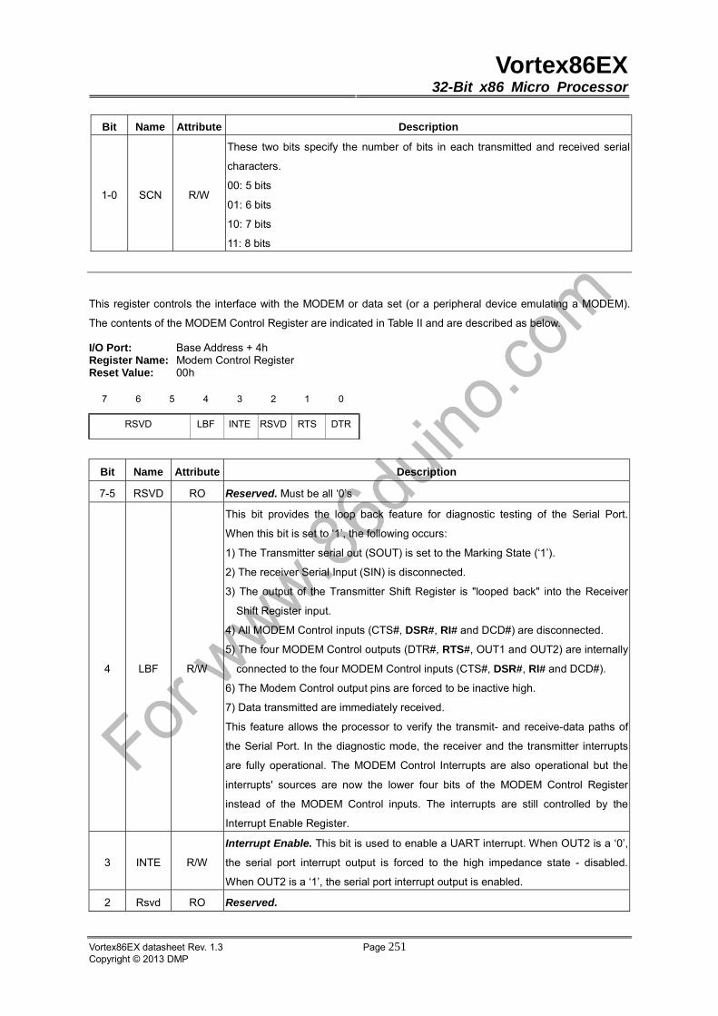
Vortex86EX32-Bit x86 Micro Processor
Vortex86EX datasheet Rev. 1.3 Page 251Copyright © 2013 DMP
Bit Name Attribute Description
1-0 SCN R/W
These two bits specify the number of bits in each transmitted and received serial
characters.
00: 5 bits
01: 6 bits
10: 7 bits
11: 8 bits
This register controls the interface with the MODEM or data set (or a peripheral device emulating a MODEM).
The contents of the MODEM Control Register are indicated in Table II and are described as below.
I/O Port: Base Address + 4h Register Name: Modem Control Register Reset Value: 00h
7 6 5 4 3 2 1 0
RSVD LBF INTE RSVD RTS DTR
Bit Name Attribute Description
7-5 RSVD RO Reserved. Must be all ‘0’s
4 LBF R/W
This bit provides the loop back feature for diagnostic testing of the Serial Port.
When this bit is set to ‘1’, the following occurs:
1) The Transmitter serial out (SOUT) is set to the Marking State (‘1’).
2) The receiver Serial Input (SIN) is disconnected.
3) The output of the Transmitter Shift Register is "looped back" into the Receiver
Shift Register input.
4) All MODEM Control inputs (CTS#, DSR#, RI# and DCD#) are disconnected.
5) The four MODEM Control outputs (DTR#, RTS#, OUT1 and OUT2) are internally
connected to the four MODEM Control inputs (CTS#, DSR#, RI# and DCD#).
6) The Modem Control output pins are forced to be inactive high.
7) Data transmitted are immediately received.
This feature allows the processor to verify the transmit- and receive-data paths of
the Serial Port. In the diagnostic mode, the receiver and the transmitter interrupts
are fully operational. The MODEM Control Interrupts are also operational but the
interrupts' sources are now the lower four bits of the MODEM Control Register
instead of the MODEM Control inputs. The interrupts are still controlled by the
Interrupt Enable Register.
3 INTE R/W
Interrupt Enable. This bit is used to enable a UART interrupt. When OUT2 is a ‘0’,
the serial port interrupt output is forced to the high impedance state - disabled.
When OUT2 is a ‘1’, the serial port interrupt output is enabled.
2 Rsvd RO Reserved.

Vortex86EX32-Bit x86 Micro Processor
Vortex86EX datasheet Rev. 1.3 Page 252Copyright © 2013 DMP
Bit Name Attribute Description
1 RTS R/W
This bit controls the Request To Send (RTS#) output. When this bit is set to a ‘1’,
the RTS# output is forced to a ‘0’. When this bit is a ‘0’, the RTS# output is forced to
a ‘1’.
0 DTR R/W
This bit controls the Data Terminal Ready (DTR#) output. When this bit is set to a
‘1’, the DTR# output is forced to a ‘0’. When this bit is a ‘0’, the DTR# output is
forced to a ‘1’.
This register provides status information to the CPU concerning the data transfer.
I/O Port: Base Address + 5h Register Name: Line Status Register Reset Value: 60h
7 6 5 4 3 2 1 0
EB TEMT THRE BI FE PE OE DR
Bit Name Attribute Description
7 EB R/W
This bit is permanently set to a logic "0" in the 450 mode. In the FIFO mode, this bit
is set to a logic "1" when there is at least one parity error, framing error or break
indication in the FIFO. This bit is cleared when the LSR is read if there are no
subsequent errors in the FIFO.
6 TEMT R/W
Transmitter Empty (TEMT). This bit is set to a ‘1’ whenever the Transmitter
Holding Register (THR) and Transmitter Shift Register (TSR) are both empty. It is
reset to a ‘0’ whenever either the THR or TSR contains a data character. This bit is
a read only bit. In the FIFO mode, this bit is set whenever the THR and TSR are
both empty,
5 THRE R/W
Transmitter Holding Register Empty (THRE). This bit indicates that the Serial
Port is ready to accept a new character for transmission. In addition, this bit causes
the Serial Port to issue an interrupt when the Transmitter Holding Register interrupt
enable is set high. The THRE bit is set to a ‘1’ when a character is transferred from
the Transmitter Holding Register into the Transmitter Shift Register. This bit is reset
to ‘0’ whenever the CPU loads the Transmitter Holding Register. In the FIFO mode,
this bit is set when the transmit FIFO is empty. It is cleared when at least 1 byte is
written to the transmit FIFO. This bit is a read only bit.
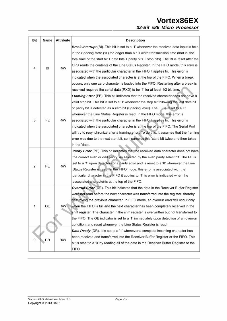
Vortex86EX32-Bit x86 Micro Processor
Vortex86EX datasheet Rev. 1.3 Page 253Copyright © 2013 DMP
Bit Name Attribute Description
4 BI R/W
Break Interrupt (BI). This bit is set to a ‘1’ whenever the received data input is held
in the Spacing state (‘0’) for longer than a full word transmission time (that is, the
total time of the start bit + data bits + parity bits + stop bits). The BI is reset after the
CPU reads the contents of the Line Status Register. In the FIFO mode, this error is
associated with the particular character in the FIFO it applies to. This error is
indicated when the associated character is at the top of the FIFO. When a break
occurs, only one zero character is loaded into the FIFO. Restarting after a break is
received requires the serial data (RXD) to be ‘1’ for at least 1/2 bit time.
3 FE R/W
Framing Error (FE). This bit indicates that the received character does not have a
valid stop bit. This bit is set to a ‘1’ whenever the stop bit following the last data bit
or parity bit is detected as a zero bit (Spacing level). The FE is reset to a ‘0’
whenever the Line Status Register is read. In the FIFO mode, this error is
associated with the particular character in the FIFO it applies to. This error is
indicated when the associated character is at the top of the FIFO. The Serial Port
will try to resynchronize after a framing error. To do this, it assumes that the framing
error was due to the next start bit, so it samples this 'start' bit twice and then takes
in the 'data'.
2 PE R/W
Parity Error (PE). This bit indicates that the received data character does not have
the correct even or odd parity, as selected by the even parity select bit. The PE is
set to a ‘1’ upon detection of a parity error and is reset to a ‘0’ whenever the Line
Status Register is read. In the FIFO mode, this error is associated with the
particular character in the FIFO it applies to. This error is indicated when the
associated character is at the top of the FIFO.
1 OE R/W
Overrun Error (OE). This bit indicates that the data in the Receiver Buffer Register
were not read before the next character was transferred into the register, thereby
destroying the previous character. In FIFO mode, an overrun error will occur only
when the FIFO is full and the next character has been completely received in the
shift register. The character in the shift register is overwritten but not transferred to
the FIFO. The OE indicator is set to a ‘1’ immediately upon detection of an overrun
condition, and reset whenever the Line Status Register is read.
0 DR R/W
Data Ready (DR). It is set to a ‘1’ whenever a complete incoming character has
been received and transferred into the Receiver Buffer Register or the FIFO. This
bit is reset to a ‘0’ by reading all of the data in the Receiver Buffer Register or the
FIFO.
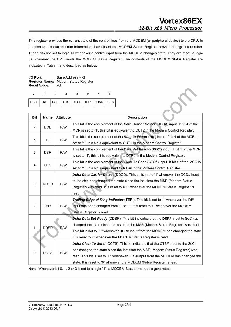
Vortex86EX32-Bit x86 Micro Processor
Vortex86EX datasheet Rev. 1.3 Page 254Copyright © 2013 DMP
This register provides the current state of the control lines from the MODEM (or peripheral device) to the CPU. In
addition to this current-state information, four bits of the MODEM Status Register provide change information.
These bits are set to logic 1s whenever a control input from the MODEM changes state. They are reset to logic
0s whenever the CPU reads the MODEM Status Register. The contents of the MODEM Status Register are
indicated in Table II and described as below.
I/O Port: Base Address + 6h Register Name: Modem Status Register Reset Value: x0h
7 6 5 4 3 2 1 0
DCD RI DSR CTS DDCD TERI DDSR DCTS
Bit Name Attribute Description
7 DCD R/W This bit is the complement of the Data Carrier Detect (DCD#) input. If bit 4 of the
MCR is set to ‘1’, this bit is equivalent to OUT2 in the Modem Control Register.
6 RI R/W This bit is the complement of the Ring Indicator (RI#) input. If bit 4 of the MCR is
set to ‘1’, this bit is equivalent to OUT1 in the Modem Control Register.
5 DSR R/W This bit is the complement of the Data Set Ready (DSR#) input. If bit 4 of the MCR
is set to ‘1’, this bit is equivalent to DTR# in the Modem Control Register.
4 CTS R/W This bit is the complement of the Clear To Send (CTS#) input. If bit 4 of the MCR is
set to ‘1’, this bit is equivalent to RTS# in the Modem Control Register.
3 DDCD R/W
Delta Data Carrier Detect (DDCD). This bit is set to ‘1’ whenever the DCD# input
to the chip has changed the state since the last time the MSR (Modem Status
Register) was read. It is reset to a ‘0’ whenever the MODEM Status Register is
read.
2 TERI R/W
Trailing Edge of Ring Indicator (TERI). This bit is set to ‘1’ whenever the RI#
input has been changed from ‘0’ to ‘1’. It is reset to ‘0’ whenever the MODEM
Status Register is read.
1 DDSR R/W
Delta Data Set Ready (DDSR). This bit indicates that the DSR# input to SoC has
changed the state since the last time the MSR (Modem Status Register) was read.
This bit is set to ‘1’" whenever DSR# input from the MODEM has changed the state.
It is reset to ‘0’ whenever the MODEM Status Register is read.
0 DCTS R/W
Delta Clear To Send (DCTS). This bit indicates that the CTS# input to the SoC
has changed the state since the last time the MSR (Modem Status Register) was
read. This bit is set to ‘1’" whenever CTS# input from the MODEM has changed the
state. It is reset to ‘0’ whenever the MODEM Status Register is read.
Note: Whenever bit 0, 1, 2 or 3 is set to a logic "1", a MODEM Status Interrupt is generated.
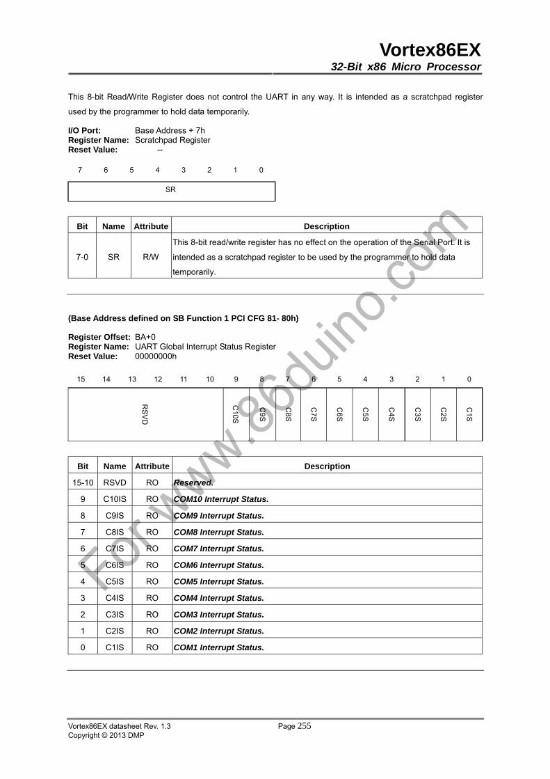
Vortex86EX32-Bit x86 Micro Processor
Vortex86EX datasheet Rev. 1.3 Page 255Copyright © 2013 DMP
This 8-bit Read/Write Register does not control the UART in any way. It is intended as a scratchpad register
used by the programmer to hold data temporarily.
I/O Port: Base Address + 7h Register Name: Scratchpad Register Reset Value: --
7 6 5 4 3 2 1 0
SR
Bit Name Attribute Description
7-0 SR R/W
This 8-bit read/write register has no effect on the operation of the Serial Port. It is
intended as a scratchpad register to be used by the programmer to hold data
temporarily.
(Base Address defined on SB Function 1 PCI CFG 81- 80h)
Register Offset: BA+0 Register Name: UART Global Interrupt Status Register Reset Value: 00000000h
15 14 13 12 11 10 9 8 7 6 5 4 3 2 1 0
Bit Name Attribute Description
15-10 RSVD RO Reserved.
9 C10IS RO COM10 Interrupt Status.
8 C9IS RO COM9 Interrupt Status.
7 C8IS RO COM8 Interrupt Status.
6 C7IS RO COM7 Interrupt Status.
5 C6IS RO COM6 Interrupt Status.
4 C5IS RO COM5 Interrupt Status.
3 C4IS RO COM4 Interrupt Status.
2 C3IS RO COM3 Interrupt Status.
1 C2IS RO COM2 Interrupt Status.
0 C1IS RO COM1 Interrupt Status.
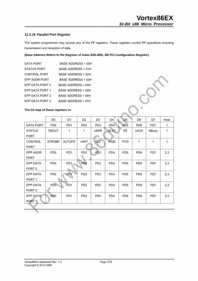
Vortex86EX32-Bit x86 Micro Processor
Vortex86EX datasheet Rev. 1.3 Page 256Copyright © 2013 DMP
11.3.16 Parallel Port Register
The system programmer may access any of the PP registers. These registers control PP operations including
transmission and reception of data.
(Base Address Refers to the Register of index B3h-B0h, SB PCI Configuration Register)
DATA PORT BASE ADDRESS + 00H
STATUS PORT BASE ADDRESS + 01H
CONTROL PORT BASE ADDRESS + 02H
EPP ADDR PORT BASE ADDRESS + 03H
EPP DATA PORT 0 BASE ADDRESS + 04H
EPP DATA PORT 1 BASE ADDRESS + 05H
EPP DATA PORT 2 BASE ADDRESS + 06H
EPP DATA PORT 3 BASE ADDRESS + 07H
The bit map of these registers is:
D0 D1 D2 D3 D4 D5 D6 D7 Note
DATA PORT PD0 PD1 PD2 PD3 PD4 PD5 PD6 PD7 1
STATUS
PORT
TMOUT 1 1 nERR SLCT PE nACK NBusy 1
CONTROL
PORT
STROBE AUTOFD nINIT SLC IRQE PCD 1 1 1
EPP ADDR
PORT
PD0 PD1 PD2 PD3 PD4 PD5 PD6 PD7 2,3
EPP DATA
PORT 0
PD0 PD1 PD2 PD3 PD4 PD5 PD6 PD7 2,3
EPP DATA
PORT 1
PD0 PD1 PD2 PD3 PD4 PD5 PD6 PD7 2,3
EPP DATA
PORT 2
PD0 PD1 PD2 PD3 PD4 PD5 PD6 PD7 2,3
EPP DATA
PORT 3
PD0 PD1 PD2 PD3 PD4 PD5 PD6 PD7 2,3
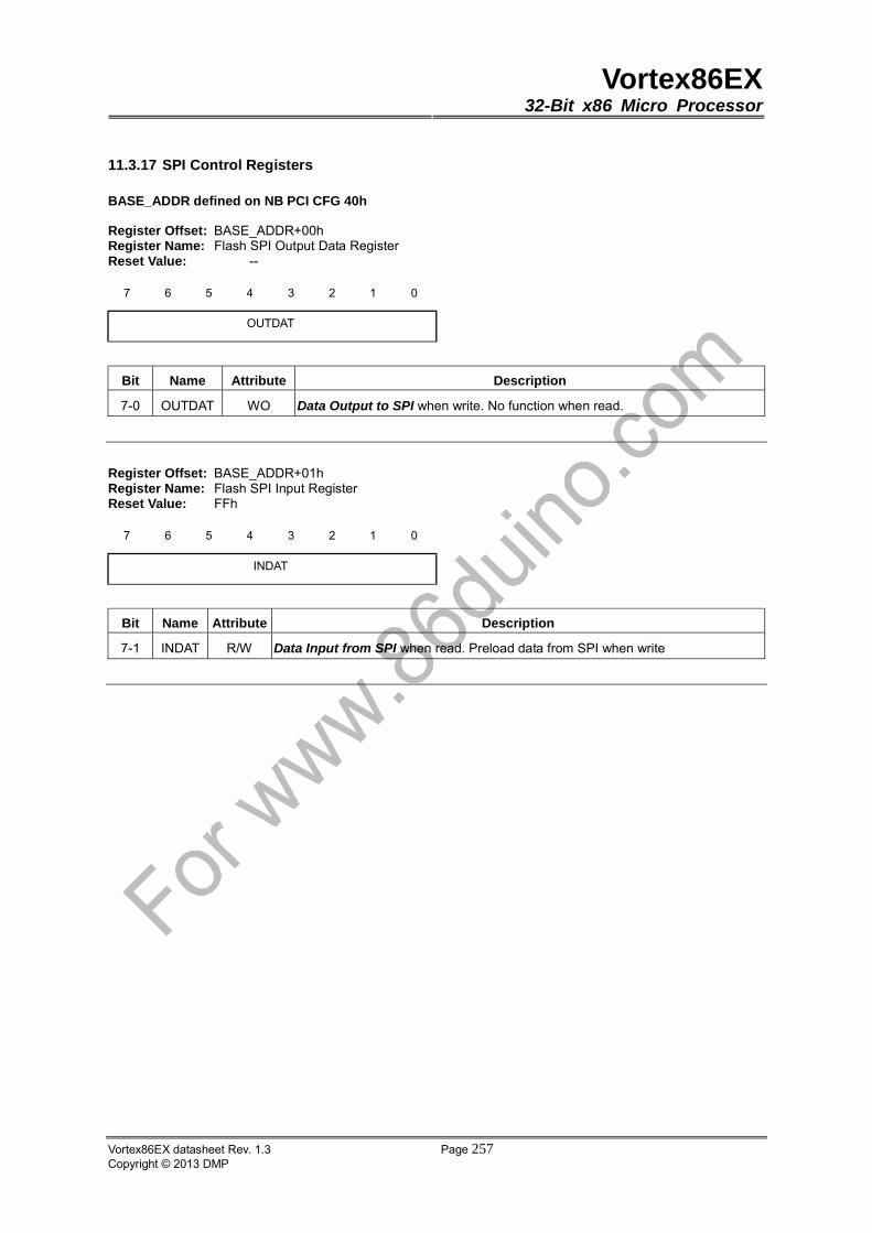
Vortex86EX32-Bit x86 Micro Processor
Vortex86EX datasheet Rev. 1.3 Page 257Copyright © 2013 DMP
11.3.17 SPI Control Registers
BASE_ADDR defined on NB PCI CFG 40h
Register Offset: BASE_ADDR+00h Register Name: Flash SPI Output Data Register Reset Value: --
7 6 5 4 3 2 1 0
OUTDAT
Bit Name Attribute Description
7-0 OUTDAT WO Data Output to SPI when write. No function when read.
Register Offset: BASE_ADDR+01h Register Name: Flash SPI Input Register Reset Value: FFh
7 6 5 4 3 2 1 0
INDAT
Bit Name Attribute Description
7-1 INDAT R/W Data Input from SPI when read. Preload data from SPI when write

Vortex86EX32-Bit x86 Micro Processor
Vortex86EX datasheet Rev. 1.3 Page 258Copyright © 2013 DMP
It is not recommended to modify this register when SPI operation.
Register Offset: BASE_ADDR+02h Register Name: Flash SPI Control Register Reset Value: 52h
7 6 5 4 3 2 1 0
RSVD FRE AFDIS FIEN CKDIV
Bit Name Attribute Description
7 RSVD RO Reserved
6 FRE R/W Fast Read Enable ( This bit can be set if it is NOT AMTEL flash, and Bit 5 must be
0 )
5 AFDIS R/W
0: Auto-fetch enable
1: Auto-fetch disable
Reset to 0 if flash ROM write protect (default).
4 FIEN R/W FIFO Mode Enable when set.
3-0 CKDIV R/W SPI Clock Divided.
The SPI clock is 100MHz/(2 * SPI clock divided) , 0 is not allowed
Register Offset: BASE_ADDR+03h Register Name: Flash SPI Status Register Reset Value: 10h
7 6 5 4 3 2 1 0
BUSY FIFU IDR ODC RSVD
Bit Name Attribute Description
7 BUSY RO SPI controller is BUSY.
6 FIFU RO FIFO Full.
5 IDR RO Input Data Ready when set.
4 ODC RO Output complete/FIFO empty when set.
3-0 RSVD RO Reserved.
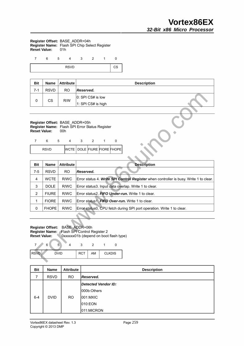
Vortex86EX32-Bit x86 Micro Processor
Vortex86EX datasheet Rev. 1.3 Page 259Copyright © 2013 DMP
Register Offset: BASE_ADDR+04h Register Name: Flash SPI Chip Select Register Reset Value: 01h
7 6 5 4 3 2 1 0
RSVD CS
Bit Name Attribute Description
7-1 RSVD RO Reserved.
0 CS R/W 0: SPI CS# is low
1: SPI CS# is high
Register Offset: BASE_ADDR+05h Register Name: Flash SPI Error Status Register Reset Value: 00h
7 6 5 4 3 2 1 0
RSVD WCTE DOLE FIURE FIORE FHOPE
Bit Name Attribute Description
7-5 RSVD RO Reserved.
4 WCTE R/WC Error status 4. Write SPI Control Register when controller is busy. Write 1 to clear.
3 DOLE R/WC Error status3. Input data overlap. Write 1 to clear.
2 FIURE R/WC Error status2, FIFO Under-run. Write 1 to clear.
1 FIORE R/WC Error status1, FIFO Over-run. Write 1 to clear.
0 FHOPE R/WC Error status0, CPU fetch during SPI port operation. Write 1 to clear.
Register Offset: BASE_ADDR+06h Register Name: Flash SPI Control Register 2 Reset Value: 0xxxxxx01b (depend on boot flash type)
7 6 5 4 3 2 1 0
RSVD DVID RCT AM CLKDIS
Bit Name Attribute Description
7 RSVD RO Reserved.
6-4 DVID RO
Detected Vendor ID:
000b:Others
001:MXIC
010:EON
011:MICRON
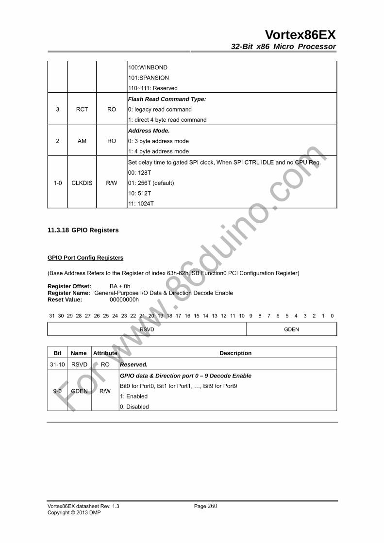
Vortex86EX32-Bit x86 Micro Processor
Vortex86EX datasheet Rev. 1.3 Page 260Copyright © 2013 DMP
100:WINBOND
101:SPANSION
110~111: Reserved
3 RCT RO
Flash Read Command Type:
0: legacy read command
1: direct 4 byte read command
2 AM RO
Address Mode.
0: 3 byte address mode
1: 4 byte address mode
1-0 CLKDIS R/W
Set delay time to gated SPI clock, When SPI CTRL IDLE and no CPU Req.
00: 128T
01: 256T (default)
10: 512T
11: 1024T
11.3.18 GPIO Registers
GPIO Port Config Registers
(Base Address Refers to the Register of index 63h-62h, SB Function0 PCI Configuration Register)
Register Offset: BA + 0h Register Name: General-Purpose I/O Data & Direction Decode Enable Reset Value: 00000000h
31 30 29 28 27 26 25 24 23 22 21 20 19 18 17 16 15 14 13 12 11 10 9 8 7 6 5 4 3 2 1 0
RSVD GDEN
Bit Name Attribute Description
31-10 RSVD RO Reserved.
9-0 GDEN R/W
GPIO data & Direction port 0 – 9 Decode Enable
Bit0 for Port0, Bit1 for Port1, …, Bit9 for Port9
1: Enabled
0: Disabled
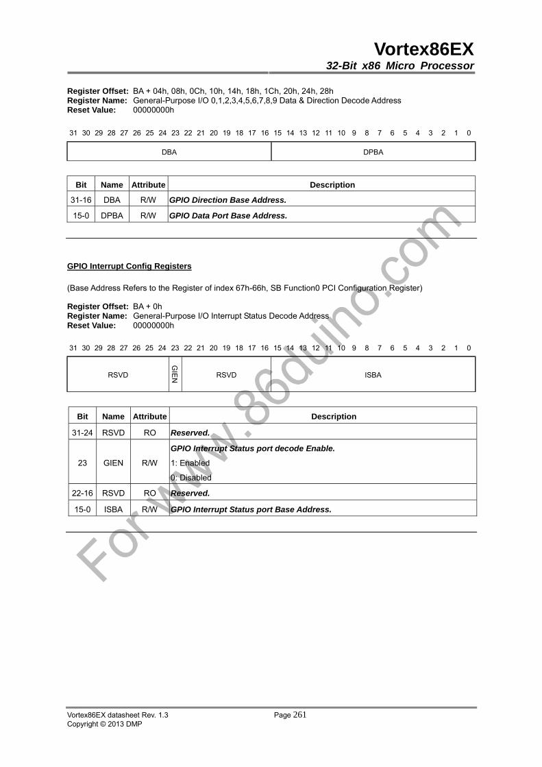
Vortex86EX32-Bit x86 Micro Processor
Vortex86EX datasheet Rev. 1.3 Page 261Copyright © 2013 DMP
Register Offset: BA + 04h, 08h, 0Ch, 10h, 14h, 18h, 1Ch, 20h, 24h, 28h Register Name: General-Purpose I/O 0,1,2,3,4,5,6,7,8,9 Data & Direction Decode Address Reset Value: 00000000h
31 30 29 28 27 26 25 24 23 22 21 20 19 18 17 16 15 14 13 12 11 10 9 8 7 6 5 4 3 2 1 0
DBA DPBA
Bit Name Attribute Description
31-16 DBA R/W GPIO Direction Base Address.
15-0 DPBA R/W GPIO Data Port Base Address.
GPIO Interrupt Config Registers
(Base Address Refers to the Register of index 67h-66h, SB Function0 PCI Configuration Register)
Register Offset: BA + 0h Register Name: General-Purpose I/O Interrupt Status Decode Address Reset Value: 00000000h
31 30 29 28 27 26 25 24 23 22 21 20 19 18 17 16 15 14 13 12 11 10 9 8 7 6 5 4 3 2 1 0
RSVD RSVD ISBA
Bit Name Attribute Description
31-24 RSVD RO Reserved.
23 GIEN R/W
GPIO Interrupt Status port decode Enable.
1: Enabled
0: Disabled
22-16 RSVD RO Reserved.
15-0 ISBA R/W GPIO Interrupt Status port Base Address.
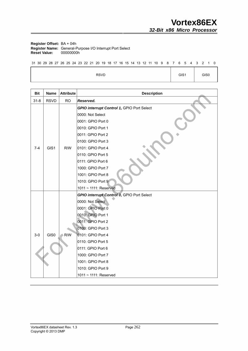
Vortex86EX32-Bit x86 Micro Processor
Vortex86EX datasheet Rev. 1.3 Page 262Copyright © 2013 DMP
Register Offset: BA + 04h Register Name: General-Purpose I/O Interrupt Port Select Reset Value: 00000000h
31 30 29 28 27 26 25 24 23 22 21 20 19 18 17 16 15 14 13 12 11 10 9 8 7 6 5 4 3 2 1 0
RSVD GIS1 GIS0
Bit Name Attribute Description
31-8 RSVD RO Reserved.
7-4 GIS1 R/W
GPIO interrupt Control 1, GPIO Port Select
0000: Not Select
0001: GPIO Port 0
0010: GPIO Port 1
0011: GPIO Port 2
0100: GPIO Port 3
0101: GPIO Port 4
0110: GPIO Port 5
0111: GPIO Port 6
1000: GPIO Port 7
1001: GPIO Port 8
1010: GPIO Port 9
1011 ~ 1111: Reserved
3-0 GIS0 R/W
GPIO interrupt Control 0, GPIO Port Select
0000: Not Select
0001: GPIO Port 0
0010: GPIO Port 1
0011: GPIO Port 2
0100: GPIO Port 3
0101: GPIO Port 4
0110: GPIO Port 5
0111: GPIO Port 6
1000: GPIO Port 7
1001: GPIO Port 8
1010: GPIO Port 9
1011 ~ 1111: Reserved
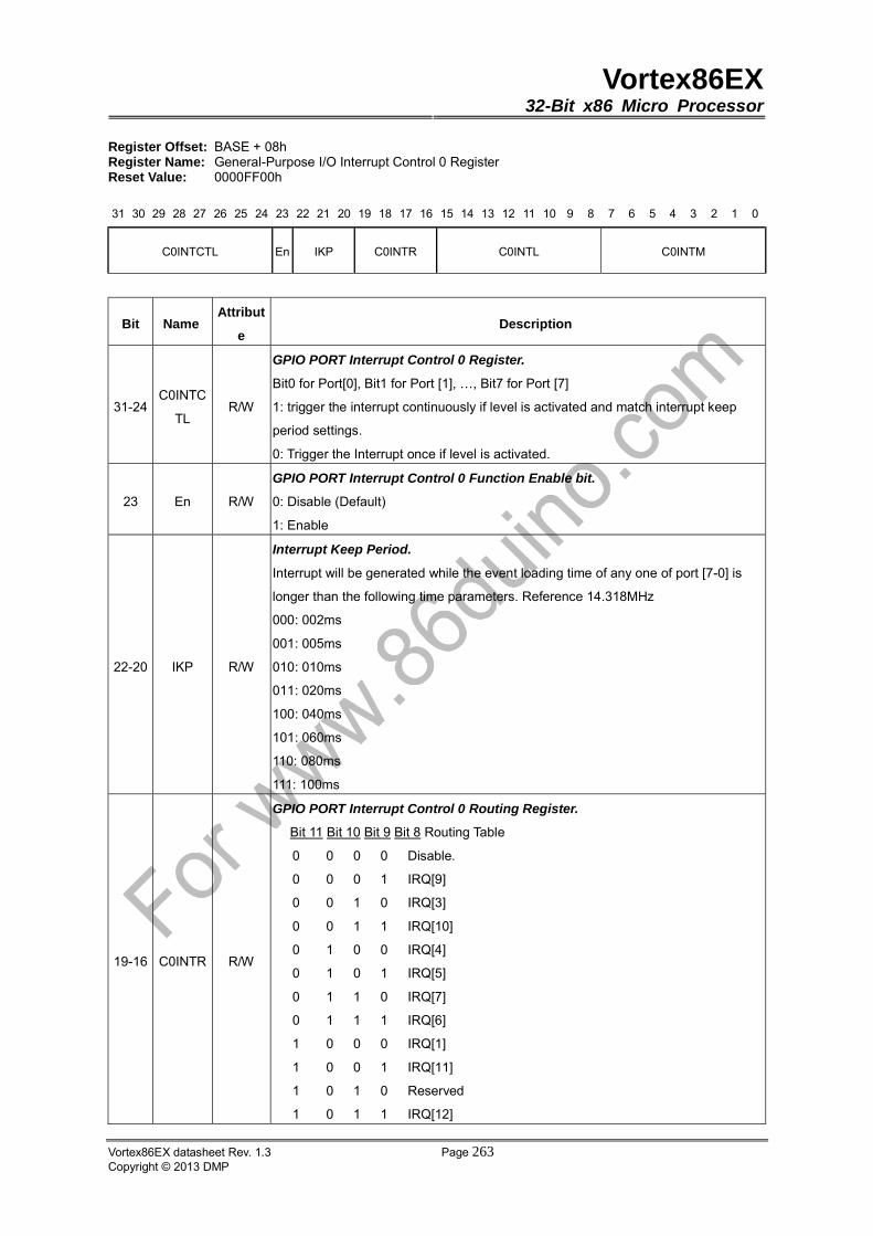
Vortex86EX32-Bit x86 Micro Processor
Vortex86EX datasheet Rev. 1.3 Page 263Copyright © 2013 DMP
Register Offset: BASE + 08h Register Name: General-Purpose I/O Interrupt Control 0 Register Reset Value: 0000FF00h
31 30 29 28 27 26 25 24 23 22 21 20 19 18 17 16 15 14 13 12 11 10 9 8 7 6 5 4 3 2 1 0
C0INTCTL En IKP C0INTR C0INTL C0INTM
Bit NameAttribut
e Description
31-24C0INTC
TL R/W
GPIO PORT Interrupt Control 0 Register.
Bit0 for Port[0], Bit1 for Port [1], …, Bit7 for Port [7]
1: trigger the interrupt continuously if level is activated and match interrupt keep
period settings.
0: Trigger the Interrupt once if level is activated.
23 En R/W
GPIO PORT Interrupt Control 0 Function Enable bit.
0: Disable (Default)
1: Enable
22-20 IKP R/W
Interrupt Keep Period.
Interrupt will be generated while the event loading time of any one of port [7-0] is
longer than the following time parameters. Reference 14.318MHz
000: 002ms
001: 005ms
010: 010ms
011: 020ms
100: 040ms
101: 060ms
110: 080ms
111: 100ms
19-16 C0INTR R/W
GPIO PORT Interrupt Control 0 Routing Register.
Bit 11 Bit 10 Bit 9 Bit 8 Routing Table
0 0 0 0 Disable.
0 0 0 1 IRQ[9]
0 0 1 0 IRQ[3]
0 0 1 1 IRQ[10]
0 1 0 0 IRQ[4]
0 1 0 1 IRQ[5]
0 1 1 0 IRQ[7]
0 1 1 1 IRQ[6]
1 0 0 0 IRQ[1]
1 0 0 1 IRQ[11]
1 0 1 0 Reserved
1 0 1 1 IRQ[12]
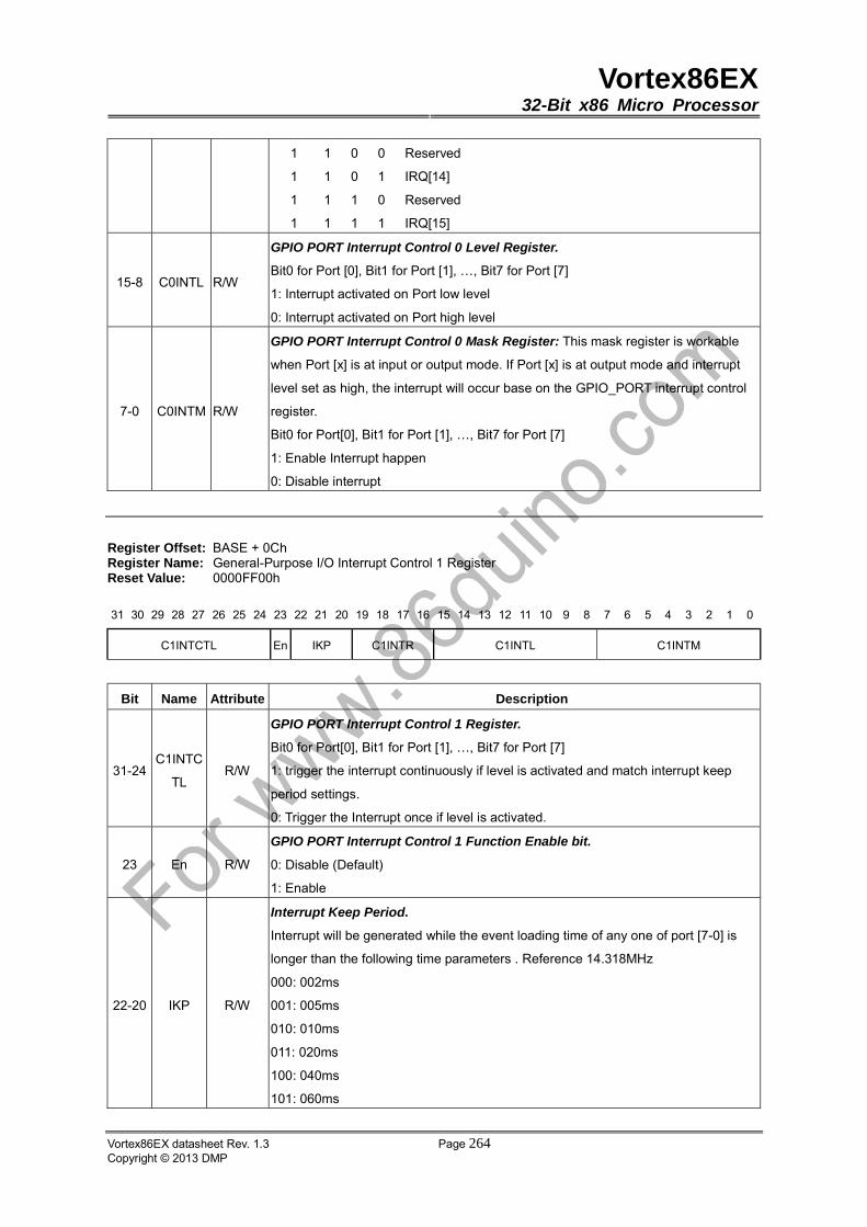
Vortex86EX32-Bit x86 Micro Processor
Vortex86EX datasheet Rev. 1.3 Page 264Copyright © 2013 DMP
1 1 0 0 Reserved
1 1 0 1 IRQ[14]
1 1 1 0 Reserved
1 1 1 1 IRQ[15]
15-8 C0INTL R/W
GPIO PORT Interrupt Control 0 Level Register.
Bit0 for Port [0], Bit1 for Port [1], …, Bit7 for Port [7]
1: Interrupt activated on Port low level
0: Interrupt activated on Port high level
7-0 C0INTM R/W
GPIO PORT Interrupt Control 0 Mask Register: This mask register is workable
when Port [x] is at input or output mode. If Port [x] is at output mode and interrupt
level set as high, the interrupt will occur base on the GPIO_PORT interrupt control
register.
Bit0 for Port[0], Bit1 for Port [1], …, Bit7 for Port [7]
1: Enable Interrupt happen
0: Disable interrupt
Register Offset: BASE + 0Ch Register Name: General-Purpose I/O Interrupt Control 1 Register Reset Value: 0000FF00h
31 30 29 28 27 26 25 24 23 22 21 20 19 18 17 16 15 14 13 12 11 10 9 8 7 6 5 4 3 2 1 0
C1INTCTL En IKP C1INTR C1INTL C1INTM
Bit Name Attribute Description
31-24C1INTC
TL R/W
GPIO PORT Interrupt Control 1 Register.
Bit0 for Port[0], Bit1 for Port [1], …, Bit7 for Port [7]
1: trigger the interrupt continuously if level is activated and match interrupt keep
period settings.
0: Trigger the Interrupt once if level is activated.
23 En R/W
GPIO PORT Interrupt Control 1 Function Enable bit.
0: Disable (Default)
1: Enable
22-20 IKP R/W
Interrupt Keep Period.
Interrupt will be generated while the event loading time of any one of port [7-0] is
longer than the following time parameters . Reference 14.318MHz
000: 002ms
001: 005ms
010: 010ms
011: 020ms
100: 040ms
101: 060ms

Vortex86EX32-Bit x86 Micro Processor
Vortex86EX datasheet Rev. 1.3 Page 265Copyright © 2013 DMP
110: 080ms
111: 100ms
19-16 C1INTR R/W
GPIO PORT Interrupt Control 1 Routing Register
Bit 11 Bit 10 Bit 9 Bit 8 Routing Table
0 0 0 0 Disable.
0 0 0 1 IRQ[9]
0 0 1 0 IRQ[3]
0 0 1 1 IRQ[10]
0 1 0 0 IRQ[4]
0 1 0 1 IRQ[5]
0 1 1 0 IRQ[7]
0 1 1 1 IRQ[6]
1 0 0 0 IRQ[1]
1 0 0 1 IRQ[11]
1 0 1 0 Reserved
1 0 1 1 IRQ[12]
1 1 0 0 Reserved
1 1 0 1 IRQ[14]
1 1 1 0 Reserved
1 1 1 1 IRQ[15]
15-8 C1INTL R/W
GPIO PORT Interrupt Control 1 Level Register.
Bit0 for Port [0], Bit1 for Port [1], …, Bit7 for Port [7]
1: Interrupt activated on Port low level
0: Interrupt activated on Port high level
7-0 C1INTM R/W
GPIO PORT Interrupt Control 1 Mask Register: This mask register is workable
when Port [x] is at input or output mode. If Port [x] is at output mode and interrupt
level set as high, the interrupt will occur base on the GPIO_PORT interrupt control
register.
Bit0 for Port[0], Bit1 for Port [1], …, Bit7 for Port [7]
1: Enable Interrupt happen
0: Disable interrupt
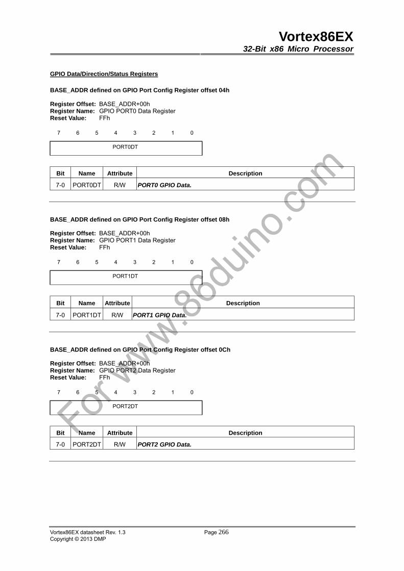
Vortex86EX32-Bit x86 Micro Processor
Vortex86EX datasheet Rev. 1.3 Page 266Copyright © 2013 DMP
GPIO Data/Direction/Status Registers
BASE_ADDR defined on GPIO Port Config Register offset 04h
Register Offset: BASE_ADDR+00h Register Name: GPIO PORT0 Data Register Reset Value: FFh
7 6 5 4 3 2 1 0
PORT0DT
Bit Name Attribute Description
7-0 PORT0DT R/W PORT0 GPIO Data.
BASE_ADDR defined on GPIO Port Config Register offset 08h
Register Offset: BASE_ADDR+00h Register Name: GPIO PORT1 Data Register Reset Value: FFh
7 6 5 4 3 2 1 0
PORT1DT
Bit Name Attribute Description
7-0 PORT1DT R/W PORT1 GPIO Data.
BASE_ADDR defined on GPIO Port Config Register offset 0Ch
Register Offset: BASE_ADDR+00h Register Name: GPIO PORT2 Data Register Reset Value: FFh
7 6 5 4 3 2 1 0
PORT2DT
Bit Name Attribute Description
7-0 PORT2DT R/W PORT2 GPIO Data.
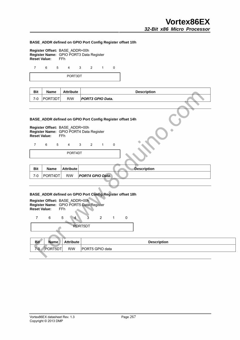
Vortex86EX32-Bit x86 Micro Processor
Vortex86EX datasheet Rev. 1.3 Page 267Copyright © 2013 DMP
BASE_ADDR defined on GPIO Port Config Register offset 10h
Register Offset: BASE_ADDR+00h Register Name: GPIO PORT3 Data Register Reset Value: FFh
7 6 5 4 3 2 1 0
PORT3DT
Bit Name Attribute Description
7-0 PORT3DT R/W PORT3 GPIO Data.
BASE_ADDR defined on GPIO Port Config Register offset 14h
Register Offset: BASE_ADDR+00h Register Name: GPIO PORT4 Data Register Reset Value: FFh
7 6 5 4 3 2 1 0
PORT4DT
Bit Name Attribute Description
7-0 PORT4DT R/W PORT4 GPIO Data.
BASE_ADDR defined on GPIO Port Config Register offset 18h
Register Offset: BASE_ADDR+00h Register Name: GPIO PORT5 Data Register Reset Value: FFh
7 6 5 4 3 2 1 0
PORT5DT
Bit Name Attribute Description
7-0 PORT5DT R/W PORT5 GPIO data
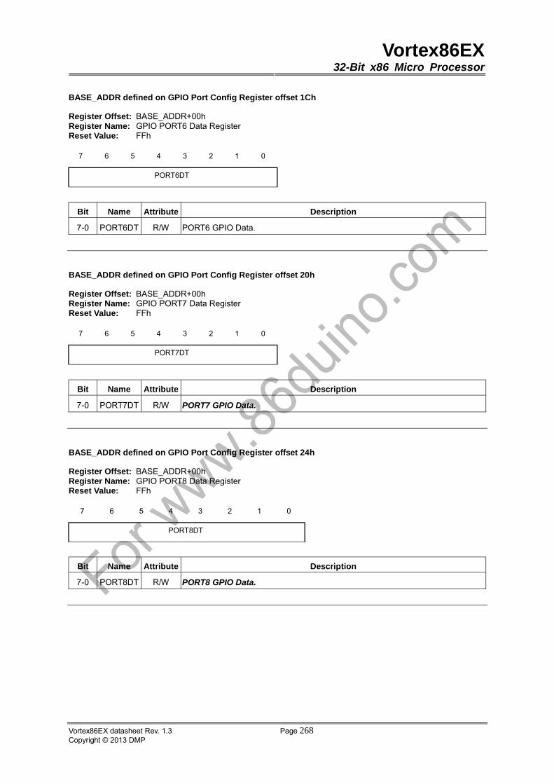
Vortex86EX32-Bit x86 Micro Processor
Vortex86EX datasheet Rev. 1.3 Page 268Copyright © 2013 DMP
BASE_ADDR defined on GPIO Port Config Register offset 1Ch
Register Offset: BASE_ADDR+00h Register Name: GPIO PORT6 Data Register Reset Value: FFh
7 6 5 4 3 2 1 0
PORT6DT
Bit Name Attribute Description
7-0 PORT6DT R/W PORT6 GPIO Data.
BASE_ADDR defined on GPIO Port Config Register offset 20h
Register Offset: BASE_ADDR+00h Register Name: GPIO PORT7 Data Register Reset Value: FFh
7 6 5 4 3 2 1 0
PORT7DT
Bit Name Attribute Description
7-0 PORT7DT R/W PORT7 GPIO Data.
BASE_ADDR defined on GPIO Port Config Register offset 24h
Register Offset: BASE_ADDR+00h Register Name: GPIO PORT8 Data Register Reset Value: FFh
7 6 5 4 3 2 1 0
PORT8DT
Bit Name Attribute Description
7-0 PORT8DT R/W PORT8 GPIO Data.
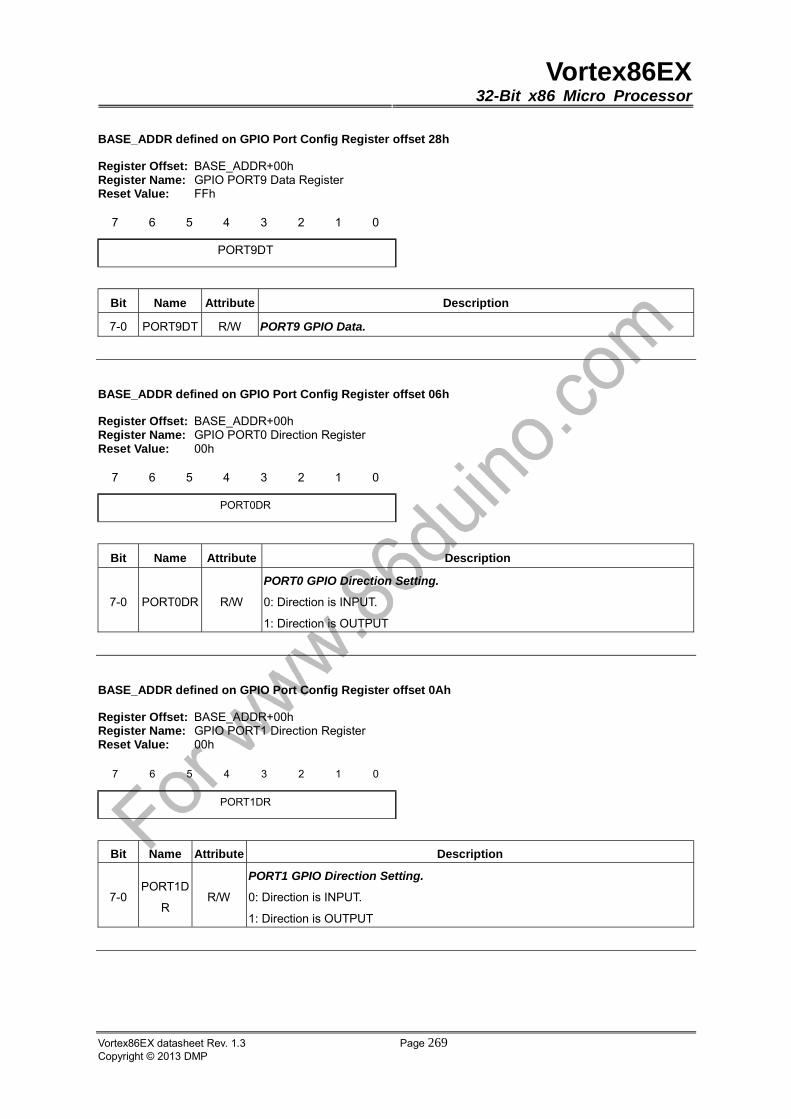
Vortex86EX32-Bit x86 Micro Processor
Vortex86EX datasheet Rev. 1.3 Page 269Copyright © 2013 DMP
BASE_ADDR defined on GPIO Port Config Register offset 28h
Register Offset: BASE_ADDR+00h Register Name: GPIO PORT9 Data Register Reset Value: FFh
7 6 5 4 3 2 1 0
PORT9DT
Bit Name Attribute Description
7-0 PORT9DT R/W PORT9 GPIO Data.
BASE_ADDR defined on GPIO Port Config Register offset 06h
Register Offset: BASE_ADDR+00h Register Name: GPIO PORT0 Direction Register Reset Value: 00h
7 6 5 4 3 2 1 0
PORT0DR
Bit Name Attribute Description
7-0 PORT0DR R/W
PORT0 GPIO Direction Setting.
0: Direction is INPUT.
1: Direction is OUTPUT
BASE_ADDR defined on GPIO Port Config Register offset 0Ah
Register Offset: BASE_ADDR+00h Register Name: GPIO PORT1 Direction Register Reset Value: 00h
7 6 5 4 3 2 1 0
PORT1DR
Bit Name Attribute Description
7-0PORT1D
R R/W
PORT1 GPIO Direction Setting.
0: Direction is INPUT.
1: Direction is OUTPUT
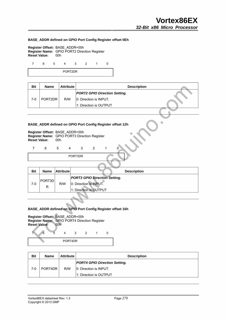
Vortex86EX32-Bit x86 Micro Processor
Vortex86EX datasheet Rev. 1.3 Page 270Copyright © 2013 DMP
BASE_ADDR defined on GPIO Port Config Register offset 0Eh
Register Offset: BASE_ADDR+00h Register Name: GPIO PORT2 Direction Register Reset Value: 00h
7 6 5 4 3 2 1 0
PORT2DR
Bit Name Attribute Description
7-0 PORT2DR R/W
PORT2 GPIO Direction Setting.
0: Direction is INPUT.
1: Direction is OUTPUT
BASE_ADDR defined on GPIO Port Config Register offset 12h
Register Offset: BASE_ADDR+00h Register Name: GPIO PORT3 Direction Register Reset Value: 00h
7 6 5 4 3 2 1 0
PORT3DR
Bit Name Attribute Description
7-0PORT3D
R R/W
PORT3 GPIO Direction Setting.
0: Direction is INPUT.
1: Direction is OUTPUT
BASE_ADDR defined on GPIO Port Config Register offset 16h
Register Offset: BASE_ADDR+00h Register Name: GPIO PORT4 Direction Register Reset Value: 00h
7 6 5 4 3 2 1 0
PORT4DR
Bit Name Attribute Description
7-0 PORT4DR R/W
PORT4 GPIO Direction Setting.
0: Direction is INPUT.
1: Direction is OUTPUT
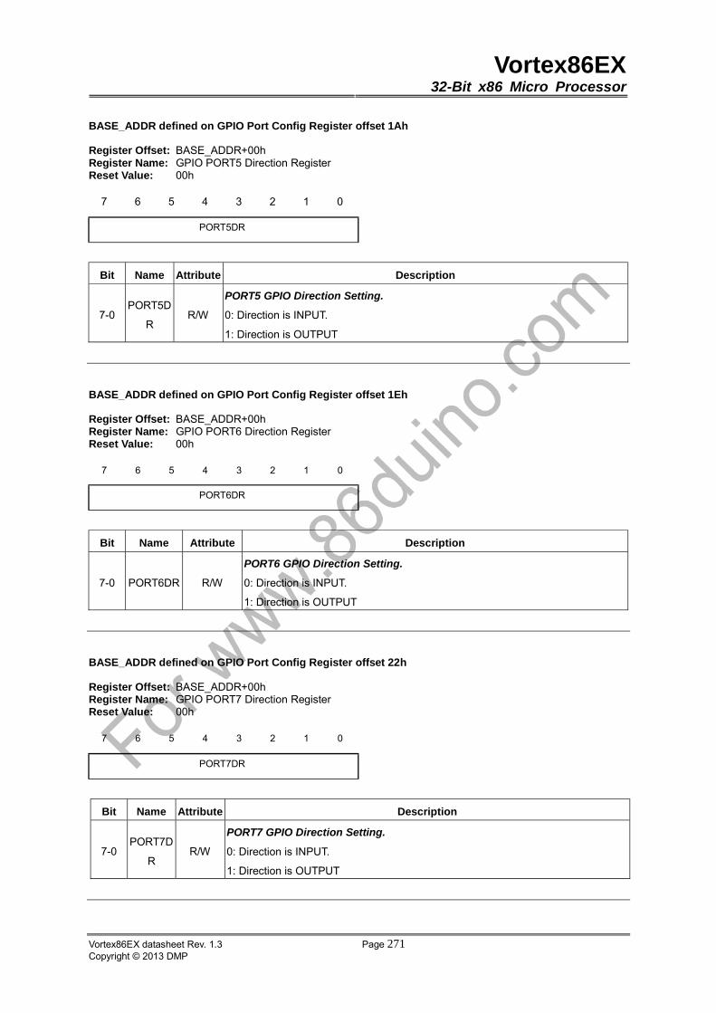
Vortex86EX32-Bit x86 Micro Processor
Vortex86EX datasheet Rev. 1.3 Page 271Copyright © 2013 DMP
BASE_ADDR defined on GPIO Port Config Register offset 1Ah
Register Offset: BASE_ADDR+00h Register Name: GPIO PORT5 Direction Register Reset Value: 00h
7 6 5 4 3 2 1 0
PORT5DR
Bit Name Attribute Description
7-0PORT5D
R R/W
PORT5 GPIO Direction Setting.
0: Direction is INPUT.
1: Direction is OUTPUT
BASE_ADDR defined on GPIO Port Config Register offset 1Eh
Register Offset: BASE_ADDR+00h Register Name: GPIO PORT6 Direction Register Reset Value: 00h
7 6 5 4 3 2 1 0
PORT6DR
Bit Name Attribute Description
7-0 PORT6DR R/W
PORT6 GPIO Direction Setting.
0: Direction is INPUT.
1: Direction is OUTPUT
BASE_ADDR defined on GPIO Port Config Register offset 22h
Register Offset: BASE_ADDR+00h Register Name: GPIO PORT7 Direction Register Reset Value: 00h
7 6 5 4 3 2 1 0
PORT7DR
Bit Name Attribute Description
7-0PORT7D
R R/W
PORT7 GPIO Direction Setting.
0: Direction is INPUT.
1: Direction is OUTPUT
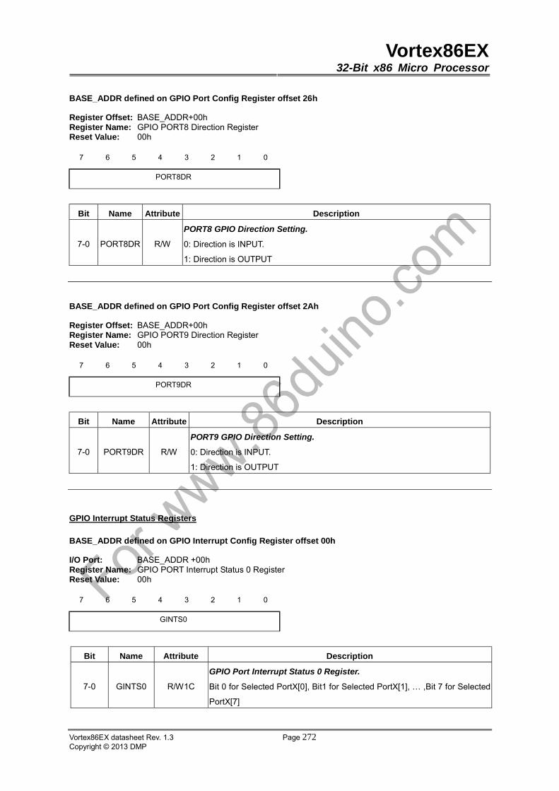
Vortex86EX32-Bit x86 Micro Processor
Vortex86EX datasheet Rev. 1.3 Page 272Copyright © 2013 DMP
BASE_ADDR defined on GPIO Port Config Register offset 26h
Register Offset: BASE_ADDR+00h Register Name: GPIO PORT8 Direction Register Reset Value: 00h
7 6 5 4 3 2 1 0
PORT8DR
Bit Name Attribute Description
7-0 PORT8DR R/W
PORT8 GPIO Direction Setting.
0: Direction is INPUT.
1: Direction is OUTPUT
BASE_ADDR defined on GPIO Port Config Register offset 2Ah
Register Offset: BASE_ADDR+00h Register Name: GPIO PORT9 Direction Register Reset Value: 00h
7 6 5 4 3 2 1 0
PORT9DR
Bit Name Attribute Description
7-0 PORT9DR R/W
PORT9 GPIO Direction Setting.
0: Direction is INPUT.
1: Direction is OUTPUT
GPIO Interrupt Status Registers
BASE_ADDR defined on GPIO Interrupt Config Register offset 00h
I/O Port: BASE_ADDR +00h Register Name: GPIO PORT Interrupt Status 0 Register Reset Value: 00h
7 6 5 4 3 2 1 0
GINTS0
Bit Name Attribute Description
7-0 GINTS0 R/W1C
GPIO Port Interrupt Status 0 Register.
Bit 0 for Selected PortX[0], Bit1 for Selected PortX[1], … ,Bit 7 for Selected
PortX[7]
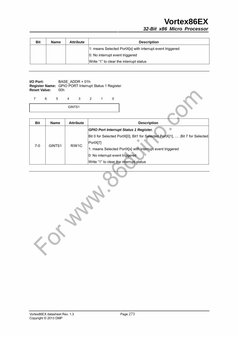
Vortex86EX32-Bit x86 Micro Processor
Vortex86EX datasheet Rev. 1.3 Page 273Copyright © 2013 DMP
Bit Name Attribute Description
1: means Selected PortX[x] with interrupt event triggered
0: No interrupt event triggered
Write “1” to clear the interrupt status
I/O Port: BASE_ADDR + 01h Register Name: GPIO PORT Interrupt Status 1 Register Reset Value: 00h
7 6 5 4 3 2 1 0
GINTS1
Bit Name Attribute Description
7-0 GINTS1 R/W1C
GPIO Port Interrupt Status 1 Register.
Bit 0 for Selected PortX[0], Bit1 for Selected PortX[1], … ,Bit 7 for Selected
PortX[7]
1: means Selected PortX[x] with interrupt event triggered
0: No interrupt event triggered
Write “1” to clear the interrupt status
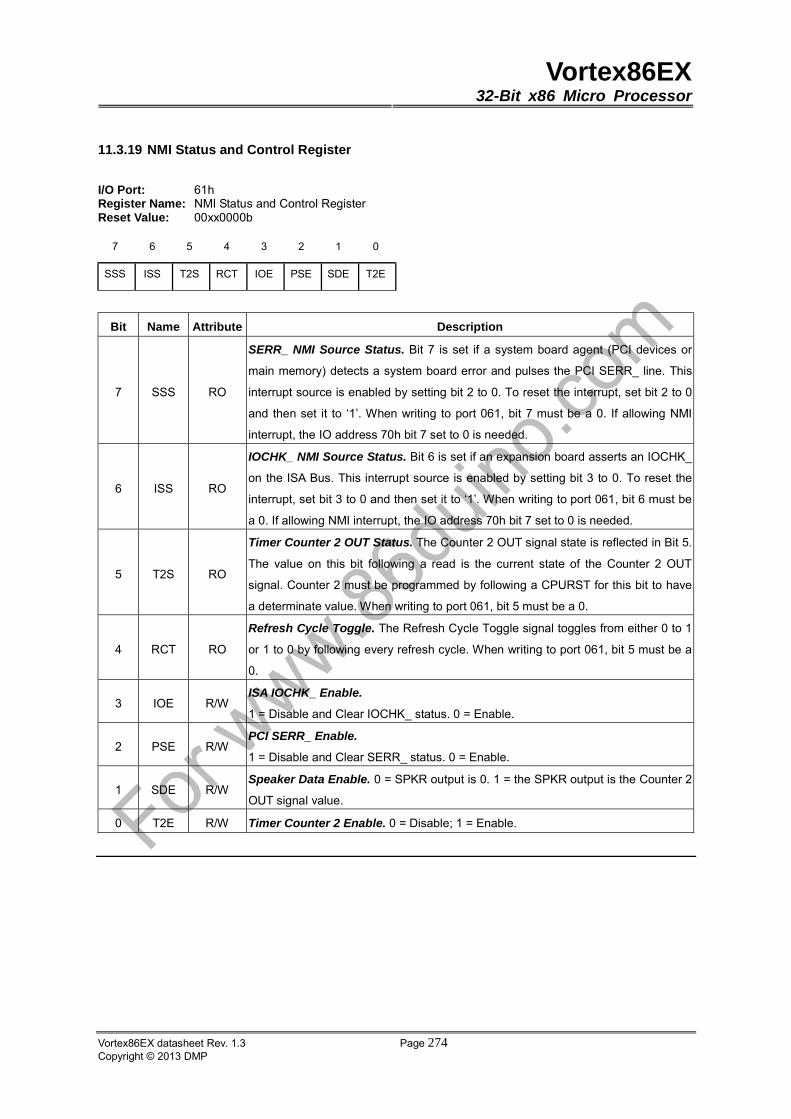
Vortex86EX32-Bit x86 Micro Processor
Vortex86EX datasheet Rev. 1.3 Page 274Copyright © 2013 DMP
11.3.19 NMI Status and Control Register
I/O Port: 61h Register Name: NMI Status and Control Register Reset Value: 00xx0000b
7 6 5 4 3 2 1 0
SSS ISS T2S RCT IOE PSE SDE T2E
Bit Name Attribute Description
7 SSS RO
SERR_ NMI Source Status. Bit 7 is set if a system board agent (PCI devices or
main memory) detects a system board error and pulses the PCI SERR_ line. This
interrupt source is enabled by setting bit 2 to 0. To reset the interrupt, set bit 2 to 0
and then set it to ‘1’. When writing to port 061, bit 7 must be a 0. If allowing NMI
interrupt, the IO address 70h bit 7 set to 0 is needed.
6 ISS RO
IOCHK_ NMI Source Status. Bit 6 is set if an expansion board asserts an IOCHK_
on the ISA Bus. This interrupt source is enabled by setting bit 3 to 0. To reset the
interrupt, set bit 3 to 0 and then set it to ‘1’. When writing to port 061, bit 6 must be
a 0. If allowing NMI interrupt, the IO address 70h bit 7 set to 0 is needed.
5 T2S RO
Timer Counter 2 OUT Status. The Counter 2 OUT signal state is reflected in Bit 5.
The value on this bit following a read is the current state of the Counter 2 OUT
signal. Counter 2 must be programmed by following a CPURST for this bit to have
a determinate value. When writing to port 061, bit 5 must be a 0.
4 RCT RO
Refresh Cycle Toggle. The Refresh Cycle Toggle signal toggles from either 0 to 1
or 1 to 0 by following every refresh cycle. When writing to port 061, bit 5 must be a
0.
3 IOE R/W ISA IOCHK_ Enable.
1 = Disable and Clear IOCHK_ status. 0 = Enable.
2 PSE R/W PCI SERR_ Enable.
1 = Disable and Clear SERR_ status. 0 = Enable.
1 SDE R/W Speaker Data Enable. 0 = SPKR output is 0. 1 = the SPKR output is the Counter 2
OUT signal value.
0 T2E R/W Timer Counter 2 Enable. 0 = Disable; 1 = Enable.
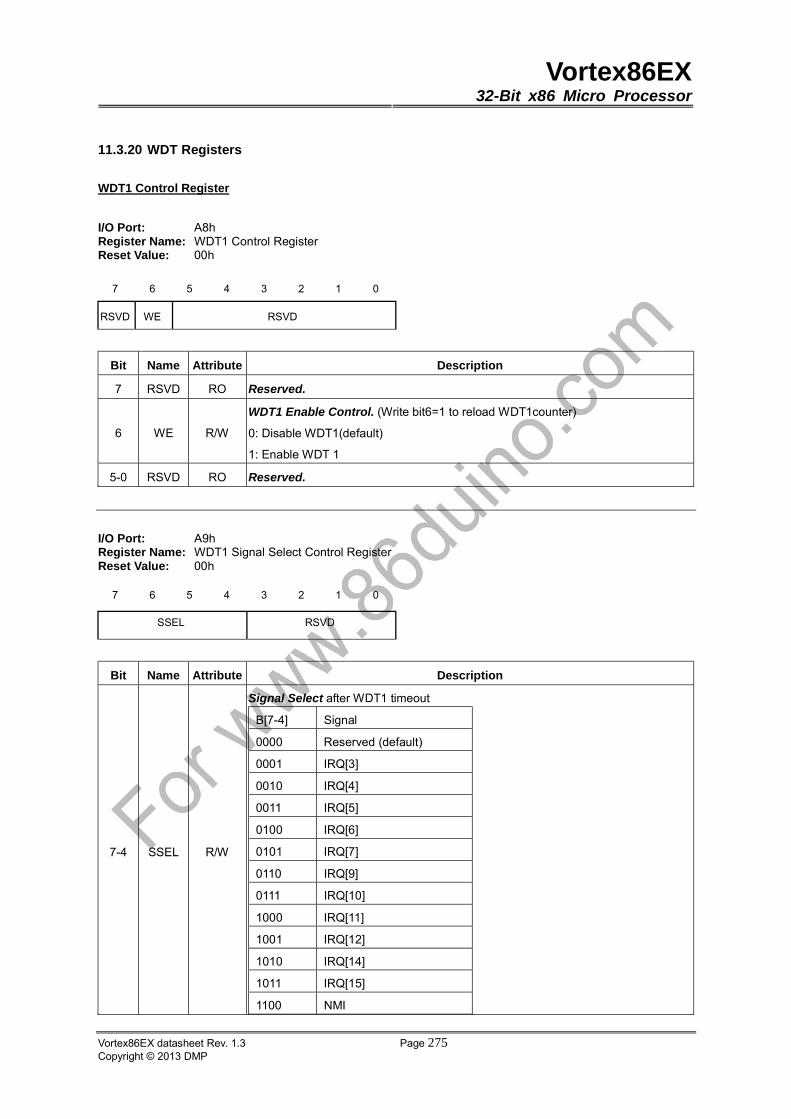
Vortex86EX32-Bit x86 Micro Processor
Vortex86EX datasheet Rev. 1.3 Page 275Copyright © 2013 DMP
11.3.20 WDT Registers
WDT1 Control Register
I/O Port: A8h Register Name: WDT1 Control Register Reset Value: 00h
7 6 5 4 3 2 1 0
RSVD WE RSVD
Bit Name Attribute Description
7 RSVD RO Reserved.
6 WE R/W
WDT1 Enable Control. (Write bit6=1 to reload WDT1counter)
0: Disable WDT1(default)
1: Enable WDT 1
5-0 RSVD RO Reserved.
I/O Port: A9h Register Name: WDT1 Signal Select Control Register Reset Value: 00h
7 6 5 4 3 2 1 0
SSEL RSVD
Bit Name Attribute Description
7-4 SSEL R/W
Signal Select after WDT1 timeout
B[7-4] Signal
0000 Reserved (default)
0001 IRQ[3]
0010 IRQ[4]
0011 IRQ[5]
0100 IRQ[6]
0101 IRQ[7]
0110 IRQ[9]
0111 IRQ[10]
1000 IRQ[11]
1001 IRQ[12]
1010 IRQ[14]
1011 IRQ[15]
1100 NMI
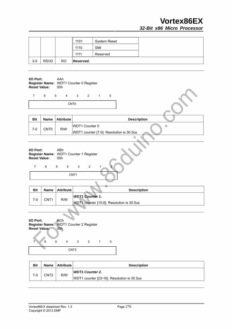
Vortex86EX32-Bit x86 Micro Processor
Vortex86EX datasheet Rev. 1.3 Page 276Copyright © 2013 DMP
1101 System Reset
1110 SMI
1111 Reserved
3-0 RSVD RO Reserved.
I/O Port: AAh Register Name: WDT1 Counter 0 Register Reset Value: 00h
7 6 5 4 3 2 1 0
CNT0
Bit Name Attribute Description
7-0 CNT0 R/W WDT1 Counter 0
WDT1 counter [7-0]. Resolution is 30.5us
I/O Port: ABh Register Name: WDT1 Counter 1 Register Reset Value: 00h
7 6 5 4 3 2 1 0
CNT1
Bit Name Attribute Description
7-0 CNT1 R/W WDT1 Counter 1.
WDT1 counter [15-8]. Resolution is 30.5us
I/O Port: ACh Register Name: WDT1 Counter 2 Register Reset Value: 00h
7 6 5 4 3 2 1 0
CNT2
Bit Name Attribute Description
7-0 CNT2 R/W WDT1 Counter 2.
WDT1 counter [23-16]. Resolution is 30.5us
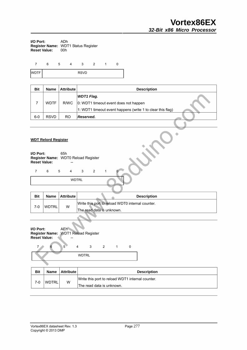
Vortex86EX32-Bit x86 Micro Processor
Vortex86EX datasheet Rev. 1.3 Page 277Copyright © 2013 DMP
I/O Port: ADh Register Name: WDT1 Status Register Reset Value: 00h
7 6 5 4 3 2 1 0
WDTF RSVD
Bit Name Attribute Description
7 WDTF R/WC
WDT1 Flag.
0: WDT1 timeout event does not happen
1: WDT1 timeout event happens (write 1 to clear this flag)
6-0 RSVD RO Reserved.
WDT Relord Register
I/O Port: 65h Register Name: WDT0 Reload Register Reset Value: --
7 6 5 4 3 2 1 0
WDTRL
Bit Name Attribute Description
7-0 WDTRL W Write this port to reload WDT0 internal counter.
The read data is unknown.
I/O Port: AEh Register Name: WDT1 Reload Register Reset Value: --
7 6 5 4 3 2 1 0
WDTRL
Bit Name Attribute Description
7-0 WDTRL W Write this port to reload WDT1 internal counter.
The read data is unknown.

Vortex86EX32-Bit x86 Micro Processor
Vortex86EX datasheet Rev. 1.3 Page 278Copyright © 2013 DMP
11.3.21 CMOS Memory & RTC Registers
This port is shared with the real-time clock. Do not modify the contents of this register without considering the
effects on the state of the other bits. Reads and writes to this register address flow through to the ISA Bus.
Reads to register 70h will cause X-Bus reads, but no RTCCS# or RTCALE will be generated. (The RTC has
traditionally been write-only to port 70h.)
I/O Port: 70h Register Name: CMOS Memory Address Register Reset Value: --
7 6 5 4 3 2 1 0
ND CRA
Bit Name Attribute Description
7 ND W = 1: NMI disabled (used in normal access to CMOS RAM)(default)
= 0: Allowed non-maskable interrupt, NMI interrupt 2
6-0 CRA W
CMOS RAM Address for the next read or write
Use SB C0h bit3 to select Page 0 or page 1.
Address 00h~14h direct access to Page0, no matter SB C0h bit3 set to 0 or 1.
I/O Port: 71h Register Name: CMOS Memory Data Register Reset Value: --
7 6 5 4 3 2 1 0
CRD
Bit Name Attribute Description
7-0 CRD W/R
RTC Data written to standard RAM bank address selected via CMOS Memory
Address
Register (70h).
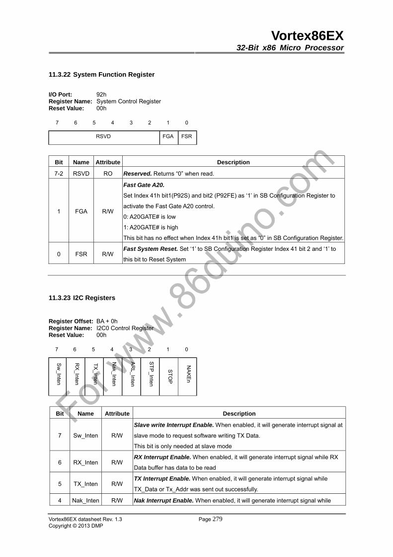
Vortex86EX32-Bit x86 Micro Processor
Vortex86EX datasheet Rev. 1.3 Page 279Copyright © 2013 DMP
11.3.22 System Function Register
I/O Port: 92h Register Name: System Control Register Reset Value: 00h
7 6 5 4 3 2 1 0
RSVD FGA FSR
Bit Name Attribute Description
7-2 RSVD RO Reserved. Returns “0” when read.
1 FGA R/W
Fast Gate A20.
Set Index 41h bit1(P92S) and bit2 (P92FE) as ‘1’ in SB Configuration Register to
activate the Fast Gate A20 control.
0: A20GATE# is low
1: A20GATE# is high
This bit has no effect when Index 41h bit1 is set as “0” in SB Configuration Register.
0 FSR R/W Fast System Reset. Set ‘1’ to SB Configuration Register Index 41 bit 2 and ‘1’ to
this bit to Reset System
11.3.23 I2C Registers
Register Offset: BA + 0h Register Name: I2C0 Control Register Reset Value: 00h
7 6 5 4 3 2 1 0
Bit Name Attribute Description
7 Sw_Inten R/W
Slave write Interrupt Enable. When enabled, it will generate interrupt signal at
slave mode to request software writing TX Data.
This bit is only needed at slave mode
6 RX_Inten R/W RX Interrupt Enable. When enabled, it will generate interrupt signal while RX
Data buffer has data to be read
5 TX_Inten R/W TX Interrupt Enable. When enabled, it will generate interrupt signal while
TX_Data or Tx_Addr was sent out successfully.
4 Nak_Inten R/W Nak Interrupt Enable. When enabled, it will generate interrupt signal while
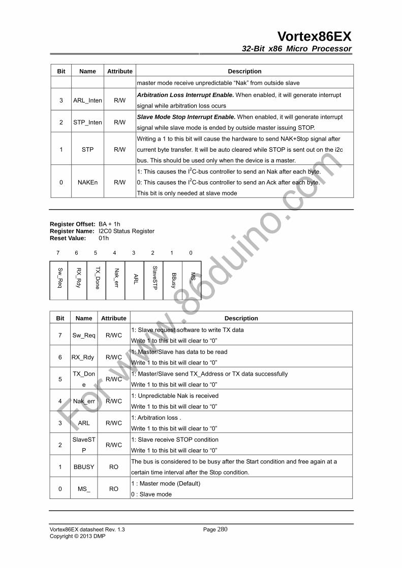
Vortex86EX32-Bit x86 Micro Processor
Vortex86EX datasheet Rev. 1.3 Page 280Copyright © 2013 DMP
Bit Name Attribute Description
master mode receive unpredictable “Nak” from outside slave
3 ARL_Inten R/W Arbitration Loss Interrupt Enable. When enabled, it will generate interrupt
signal while arbitration loss ocurs
2 STP_Inten R/W Slave Mode Stop Interrupt Enable. When enabled, it will generate interrupt
signal while slave mode is ended by outside master issuing STOP.
1 STP R/W
Writing a 1 to this bit will cause the hardware to send NAK+Stop signal after
current byte transfer. It will be auto cleared while STOP is sent out on the i2c
bus. This should be used only when the device is a master.
0 NAKEn R/W
1: This causes the I2C-bus controller to send an Nak after each byte.
0: This causes the I2C-bus controller to send an Ack after each byte.
This bit is only needed at slave mode
Register Offset: BA + 1h Register Name: I2C0 Status Register Reset Value: 01h
7 6 5 4 3 2 1 0
Bit Name Attribute Description
7 Sw_Req R/WC 1: Slave request software to write TX data
Write 1 to this bit will clear to “0”
6 RX_Rdy R/WC 1: Master/Slave has data to be read
Write 1 to this bit will clear to “0”
5 TX_Don
e R/WC
1: Master/Slave send TX_Address or TX data successfully
Write 1 to this bit will clear to “0”
4 Nak_err R/WC 1: Unpredictable Nak is received
Write 1 to this bit will clear to “0”
3 ARL R/WC 1: Arbitration loss .
Write 1 to this bit will clear to “0”
2 SlaveST
P R/WC
1: Slave receive STOP condition
Write 1 to this bit will clear to “0”
1 BBUSY RO The bus is considered to be busy after the Start condition and free again at a
certain time interval after the Stop condition.
0 MS_ RO 1 : Master mode (Default)
0 : Slave mode

Vortex86EX32-Bit x86 Micro Processor
Vortex86EX datasheet Rev. 1.3 Page 281Copyright © 2013 DMP
Register Offset: BA + 2h Register Name: I2C0 My_Address Register Reset Value: 00h
7 6 5 4 3 2 1 0
My Slave Address TCE
Bit Name Attribute Description
7-1 My_Addr R/W
7-bits slave address which is checked by internal slave module. If address is
match it will switch to slave mode. Processor can write proper value into this
register to identify itself
0 TCE R/W
I2C START/STOP timing constraint is dynamic with the clock rate setting.
(Max(half of clock cycle, spec timing))
1: Enabled
0: Disabled
Register Offset: BA + 3h Register Name: I2C0 Transmit Address Register Reset Value: 00h
7 6 5 4 3 2 1 0
TX Slave Address R/W
Bit Name Attribute Description
7-0TX_Add
r R/W
8-bit address register for Master to start a transaction. Processor can write this
register to generate START + Slave Address + R/W on i2c bus. If Processor writes
a macrocode into this register, it will send out macrocode and switch to high-speed
mode at proper timing.
Register Offset: BA + 4h Register Name: I2C0 Transmit/Receive Data Register Reset Value: 00h
7 6 5 4 3 2 1 0
Data
Bit Name Attribute Description
7-0 Data R/W 8-bit data register for I2C-bus Tx/Rx operation. Processor can write this register to
transmit DATA or read this register to receive data.
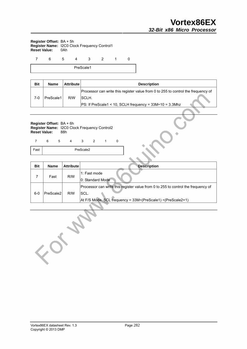
Vortex86EX32-Bit x86 Micro Processor
Vortex86EX datasheet Rev. 1.3 Page 282Copyright © 2013 DMP
Register Offset: BA + 5h Register Name: I2C0 Clock Frequency Control1 Reset Value: 0Ah
7 6 5 4 3 2 1 0
PreScale1
Bit Name Attribute Description
7-0 PreScale1 R/W
Processor can write this register value from 0 to 255 to control the frequency of
SCLH.
PS: If PreScale1 < 10, SCLH frequency = 33M÷10 = 3.3Mhz
Register Offset: BA + 6h Register Name: I2C0 Clock Frequency Control2 Reset Value: 88h
7 6 5 4 3 2 1 0
Fast PreScale2
Bit Name Attribute Description
7 Fast R/W 1: Fast mode
0: Standard Mode
6-0 PreScale2 R/W
Processor can write this register value from 0 to 255 to control the frequency of
SCL.
At F/S Mode, SCL frequency = 33M÷(PreScale1) ÷(PreScale2+1)
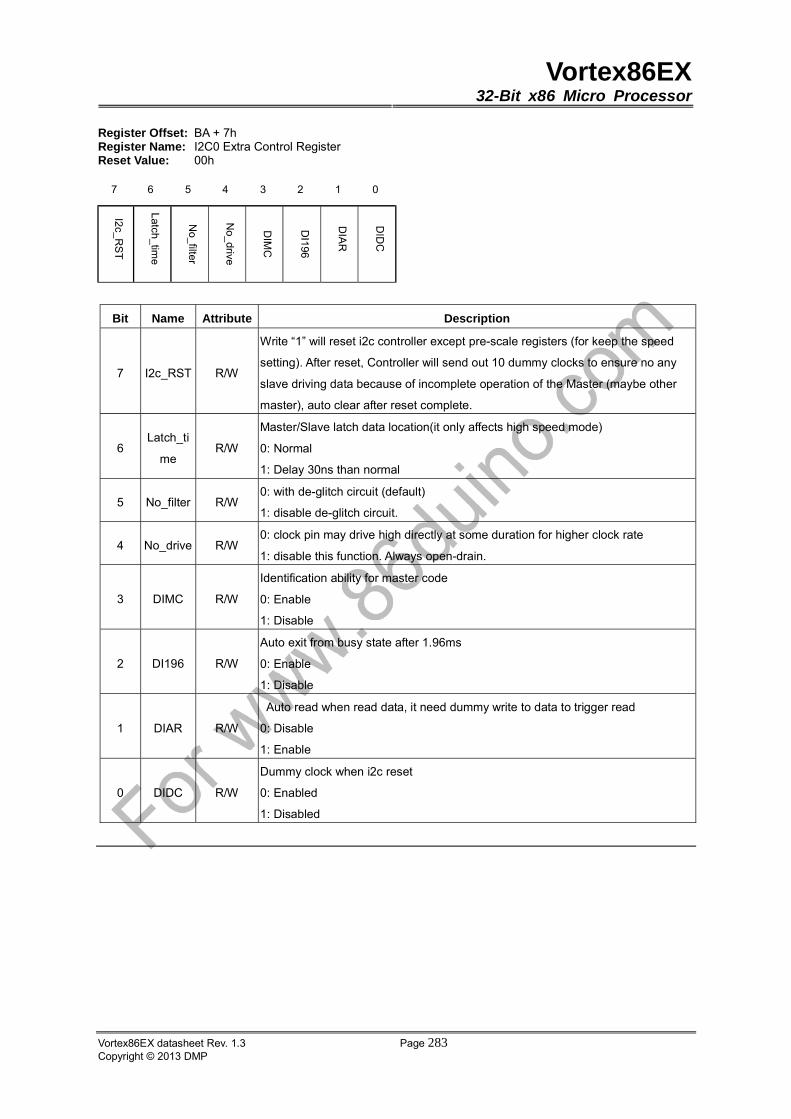
Vortex86EX32-Bit x86 Micro Processor
Vortex86EX datasheet Rev. 1.3 Page 283Copyright © 2013 DMP
Register Offset: BA + 7h Register Name: I2C0 Extra Control Register Reset Value: 00h
7 6 5 4 3 2 1 0
Bit Name Attribute Description
7 I2c_RST R/W
Write “1” will reset i2c controller except pre-scale registers (for keep the speed
setting). After reset, Controller will send out 10 dummy clocks to ensure no any
slave driving data because of incomplete operation of the Master (maybe other
master), auto clear after reset complete.
6 Latch_ti
me R/W
Master/Slave latch data location(it only affects high speed mode)
0: Normal
1: Delay 30ns than normal
5 No_filter R/W 0: with de-glitch circuit (default)
1: disable de-glitch circuit.
4 No_drive R/W 0: clock pin may drive high directly at some duration for higher clock rate
1: disable this function. Always open-drain.
3 DIMC R/W
Identification ability for master code
0: Enable
1: Disable
2 DI196 R/W
Auto exit from busy state after 1.96ms
0: Enable
1: Disable
1 DIAR R/W
Auto read when read data, it need dummy write to data to trigger read
0: Disable
1: Enable
0 DIDC R/W
Dummy clock when i2c reset
0: Enabled
1: Disabled
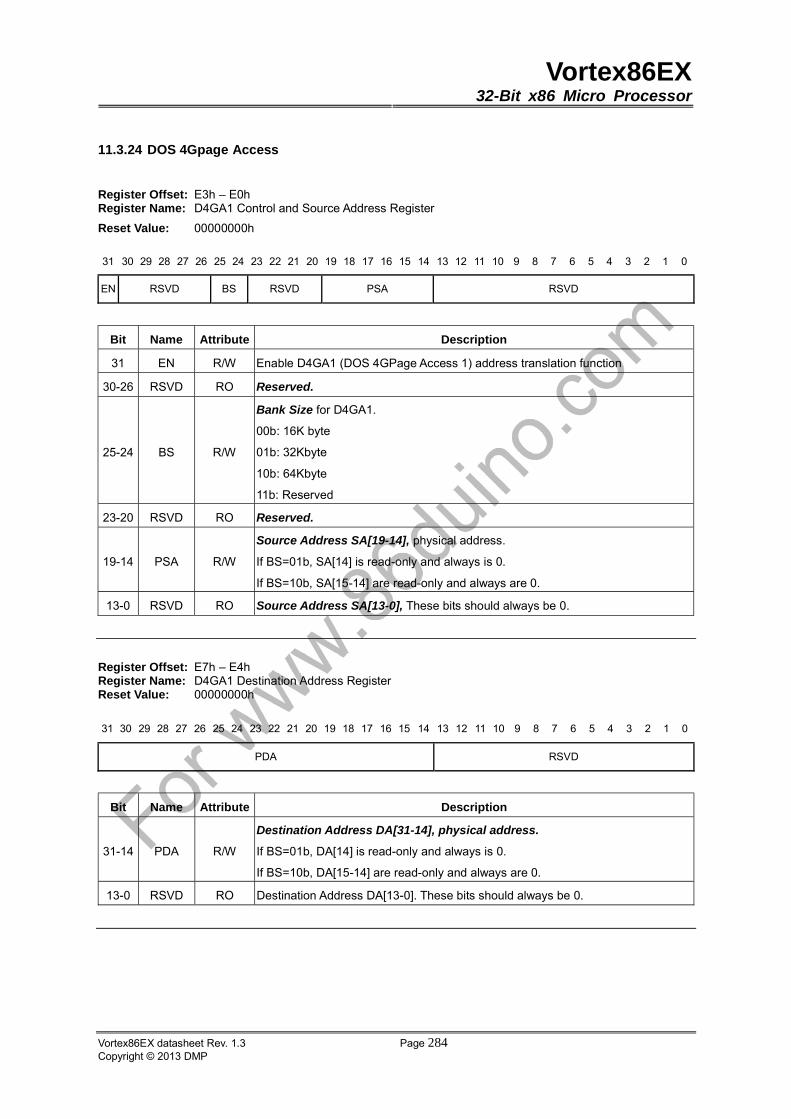
Vortex86EX32-Bit x86 Micro Processor
Vortex86EX datasheet Rev. 1.3 Page 284Copyright © 2013 DMP
11.3.24 DOS 4Gpage Access
Register Offset: E3h – E0h Register Name: D4GA1 Control and Source Address Register
Reset Value: 00000000h
31 30 29 28 27 26 25 24 23 22 21 20 19 18 17 16 15 14 13 12 11 10 9 8 7 6 5 4 3 2 1 0
EN RSVD BS RSVD PSA RSVD
Bit Name Attribute Description
31 EN R/W Enable D4GA1 (DOS 4GPage Access 1) address translation function
30-26 RSVD RO Reserved.
25-24 BS R/W
Bank Size for D4GA1.
00b: 16K byte
01b: 32Kbyte
10b: 64Kbyte
11b: Reserved
23-20 RSVD RO Reserved.
19-14 PSA R/W
Source Address SA[19-14], physical address.
If BS=01b, SA[14] is read-only and always is 0.
If BS=10b, SA[15-14] are read-only and always are 0.
13-0 RSVD RO Source Address SA[13-0], These bits should always be 0.
Register Offset: E7h – E4h Register Name: D4GA1 Destination Address Register Reset Value: 00000000h
31 30 29 28 27 26 25 24 23 22 21 20 19 18 17 16 15 14 13 12 11 10 9 8 7 6 5 4 3 2 1 0
PDA RSVD
Bit Name Attribute Description
31-14 PDA R/W
Destination Address DA[31-14], physical address.
If BS=01b, DA[14] is read-only and always is 0.
If BS=10b, DA[15-14] are read-only and always are 0.
13-0 RSVD RO Destination Address DA[13-0]. These bits should always be 0.
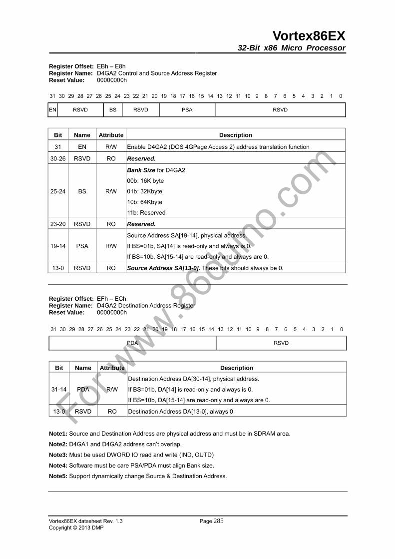
Vortex86EX32-Bit x86 Micro Processor
Vortex86EX datasheet Rev. 1.3 Page 285Copyright © 2013 DMP
Register Offset: EBh – E8h Register Name: D4GA2 Control and Source Address Register Reset Value: 00000000h
31 30 29 28 27 26 25 24 23 22 21 20 19 18 17 16 15 14 13 12 11 10 9 8 7 6 5 4 3 2 1 0
EN RSVD BS RSVD PSA RSVD
Bit Name Attribute Description
31 EN R/W Enable D4GA2 (DOS 4GPage Access 2) address translation function
30-26 RSVD RO Reserved.
25-24 BS R/W
Bank Size for D4GA2.
00b: 16K byte
01b: 32Kbyte
10b: 64Kbyte
11b: Reserved
23-20 RSVD RO Reserved.
19-14 PSA R/W
Source Address SA[19-14], physical address.
If BS=01b, SA[14] is read-only and always is 0.
If BS=10b, SA[15-14] are read-only and always are 0.
13-0 RSVD RO Source Address SA[13-0]. These bits should always be 0.
Register Offset: EFh – ECh Register Name: D4GA2 Destination Address Register Reset Value: 00000000h
31 30 29 28 27 26 25 24 23 22 21 20 19 18 17 16 15 14 13 12 11 10 9 8 7 6 5 4 3 2 1 0
PDA RSVD
Bit Name Attribute Description
31-14 PDA R/W
Destination Address DA[30-14], physical address.
If BS=01b, DA[14] is read-only and always is 0.
If BS=10b, DA[15-14] are read-only and always are 0.
13-0 RSVD RO Destination Address DA[13-0], always 0
Note1: Source and Destination Address are physical address and must be in SDRAM area.
Note2: D4GA1 and D4GA2 address can’t overlap.
Note3: Must be used DWORD IO read and write (IND, OUTD)
Note4: Software must be care PSA/PDA must align Bank size.
Note5: Support dynamically change Source & Destination Address.
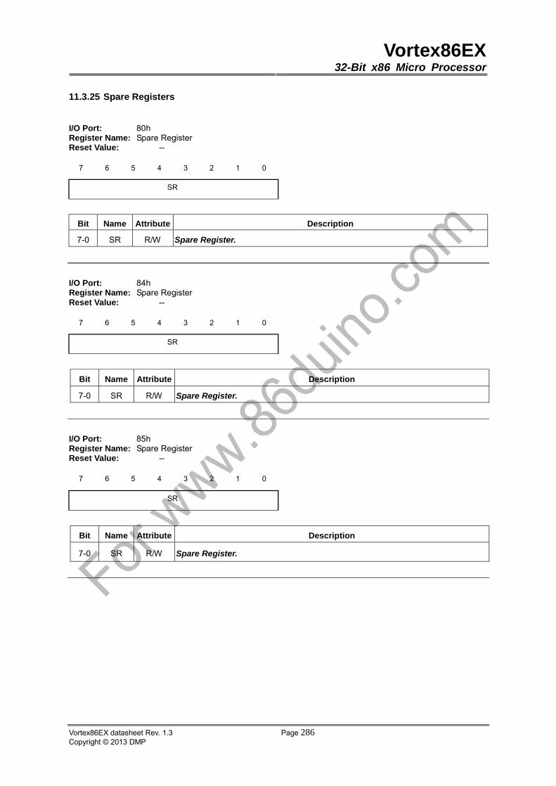
Vortex86EX32-Bit x86 Micro Processor
Vortex86EX datasheet Rev. 1.3 Page 286Copyright © 2013 DMP
11.3.25 Spare Registers
I/O Port: 80h Register Name: Spare Register Reset Value: --
7 6 5 4 3 2 1 0
SR
Bit Name Attribute Description
7-0 SR R/W Spare Register.
I/O Port: 84h Register Name: Spare Register Reset Value: --
7 6 5 4 3 2 1 0
SR
Bit Name Attribute Description
7-0 SR R/W Spare Register.
I/O Port: 85h Register Name: Spare Register Reset Value: --
7 6 5 4 3 2 1 0
SR
Bit Name Attribute Description
7-0 SR R/W Spare Register.

Vortex86EX32-Bit x86 Micro Processor
Vortex86EX datasheet Rev. 1.3 Page 287Copyright © 2013 DMP
I/O Port: 86h Register Name: Spare Register Reset Value: --
7 6 5 4 3 2 1 0
SR
Bit Name Attribute Description
7-0 SR R/W Spare Register.
I/O Port: 88h Register Name: Spare Register Reset Value: --
7 6 5 4 3 2 1 0
SR
Bit Name Attribute Description
7-0 SR R/W Spare Register.
I/O Port: 8Ch Register Name: Spare Register Reset Value: --
7 6 5 4 3 2 1 0
SR
Bit Name Attribute Description
7-0 SR R/W Spare Register.
I/O Port: 8Dh Register Name: Spare Register Reset Value: --
7 6 5 4 3 2 1 0
SR
Bit Name Attribute Description
7-0 SR R/W Spare Register.
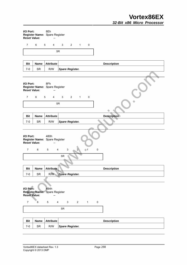
Vortex86EX32-Bit x86 Micro Processor
Vortex86EX datasheet Rev. 1.3 Page 288Copyright © 2013 DMP
I/O Port: 8Eh Register Name: Spare Register Reset Value: --
7 6 5 4 3 2 1 0
SR
Bit Name Attribute Description
7-0 SR R/W Spare Register.
I/O Port: 8Fh Register Name: Spare Register Reset Value: --
7 6 5 4 3 2 1 0
SR
Bit Name Attribute Description
7-0 SR R/W Spare Register.
I/O Port: 480h Register Name: Spare Register Reset Value: --
7 6 5 4 3 2 1 0
SR
Bit Name Attribute Description
7-0 SR R/W Spare Register.
I/O Port: 484h Register Name: Spare Register Reset Value: --
7 6 5 4 3 2 1 0
SR
Bit Name Attribute Description
7-0 SR R/W Spare Register.

Vortex86EX32-Bit x86 Micro Processor
Vortex86EX datasheet Rev. 1.3 Page 289Copyright © 2013 DMP
I/O Port: 485h Register Name: Spare Register Reset Value: --
7 6 5 4 3 2 1 0
SR
Bit Name Attribute Description
7-0 SR R/W Spare Register.
I/O Port: 486h Register Name: Spare Register Reset Value: --
7 6 5 4 3 2 1 0
SR
Bit Name Attribute Description
7-0 SR R/W Spare Register.
I/O Port: 488h Register Name: Spare Register Reset Value: --
7 6 5 4 3 2 1 0
SR
Bit Name Attribute Description
7-0 SR R/W Spare Register.
I/O Port: 48Ch Register Name: Spare Register Reset Value: --
7 6 5 4 3 2 1 0
SR
Bit Name Attribute Description
7-0 SR R/W Spare Register.
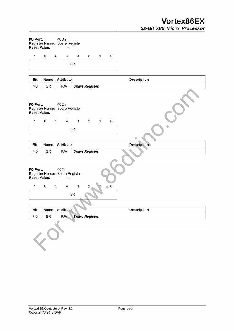
Vortex86EX32-Bit x86 Micro Processor
Vortex86EX datasheet Rev. 1.3 Page 290Copyright © 2013 DMP
I/O Port: 48Dh Register Name: Spare Register Reset Value: --
7 6 5 4 3 2 1 0
SR
Bit Name Attribute Description
7-0 SR R/W Spare Register.
I/O Port: 48Eh Register Name: Spare Register Reset Value: --
7 6 5 4 3 2 1 0
SR
Bit Name Attribute Description
7-0 SR R/W Spare Register.
I/O Port: 48Fh Register Name: Spare Register Reset Value: --
7 6 5 4 3 2 1 0
SR
Bit Name Attribute Description
7-0 SR R/W Spare Register.

Vortex86EX32-Bit x86 Micro Processor
Vortex86EX datasheet Rev. 1.3 Page 291Copyright © 2013 DMP
11.3.26 SMM Registers
I/O Port: 0B2h Register Name: Software SMI Trigger Port2 Reset Value: 00h
7 6 5 4 3 2 1 0
SMIT
Bit Name Attribute Description
7-0 SMIT R/W Generate a software SMI when write this port. This port is useful when SMI
function Control register bit0 = 1.
Register Offset: BA+0 Register Name: SMI Event Status Register Reset Value: 00000000h
31 30 29 28 27 26 25 24 23 22 21 20 19 18 17 16 15 14 13 12 11 10 9 8 7 6 5 4 3 2 1 0
SSS W1SR RSVD U0ERU0ORSSR1SSR0
Bit Name Attribute Description
31 SSS R/WC SMI Summary Status. If there is at least one SMI request that enabled by SMI
Control Register. This bit will be ‘1’.
30 W1SR R/WC WDT1 SMI Request Event happens when Set. Write 1 to Clear.
29-4 RSVD RO Reserved.
3 U0ER R/WC USB0 EHCI SMI Request Event happens when Set. Write 1 to Clear.
2 U0OR R/WC USB0 OHCI SMI Request Event happens when Set. Write 1 to Clear.
1 SSR1 R/WC Software SMI Request Event happens from port B2h when Set. Write 1 to Clear.
0 SSR0 R/WC Software SMI Request Event happens from port BA+10 when Set. Write 1 to
Clear.
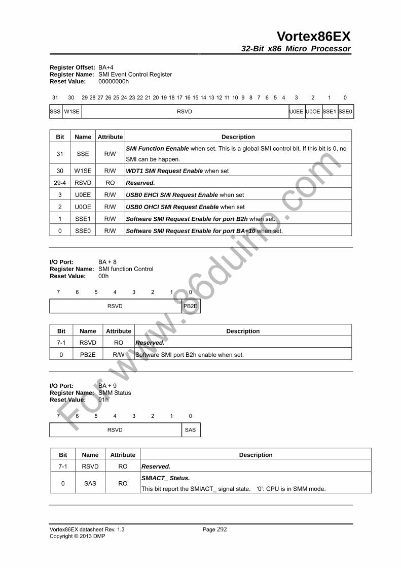
Vortex86EX32-Bit x86 Micro Processor
Vortex86EX datasheet Rev. 1.3 Page 292Copyright © 2013 DMP
Register Offset: BA+4 Register Name: SMI Event Control Register Reset Value: 00000000h
31 30 29 28 27 26 25 24 23 22 21 20 19 18 17 16 15 14 13 12 11 10 9 8 7 6 5 4 3 2 1 0
SSS W1SE RSVD U0EE U0OE SSE1 SSE0
Bit Name Attribute Description
31 SSE R/W SMI Function Eenable when set. This is a global SMI control bit. If this bit is 0, no
SMI can be happen.
30 W1SE R/W WDT1 SMI Request Enable when set
29-4 RSVD RO Reserved.
3 U0EE R/W USB0 EHCI SMI Request Enable when set
2 U0OE R/W USB0 OHCI SMI Request Enable when set
1 SSE1 R/W Software SMI Request Enable for port B2h when set.
0 SSE0 R/W Software SMI Request Enable for port BA+10 when set.
I/O Port: BA + 8 Register Name: SMI function Control Reset Value: 00h
7 6 5 4 3 2 1 0
RSVD PB2E
Bit Name Attribute Description
7-1 RSVD RO Reserved.
0 PB2E R/W Software SMI port B2h enable when set.
I/O Port: BA + 9 Register Name: SMM Status Reset Value: 01h
7 6 5 4 3 2 1 0
RSVD SAS
Bit Name Attribute Description
7-1 RSVD RO Reserved.
0 SAS RO SMIACT_ Status.
This bit report the SMIACT_ signal state. ‘0’: CPU is in SMM mode.
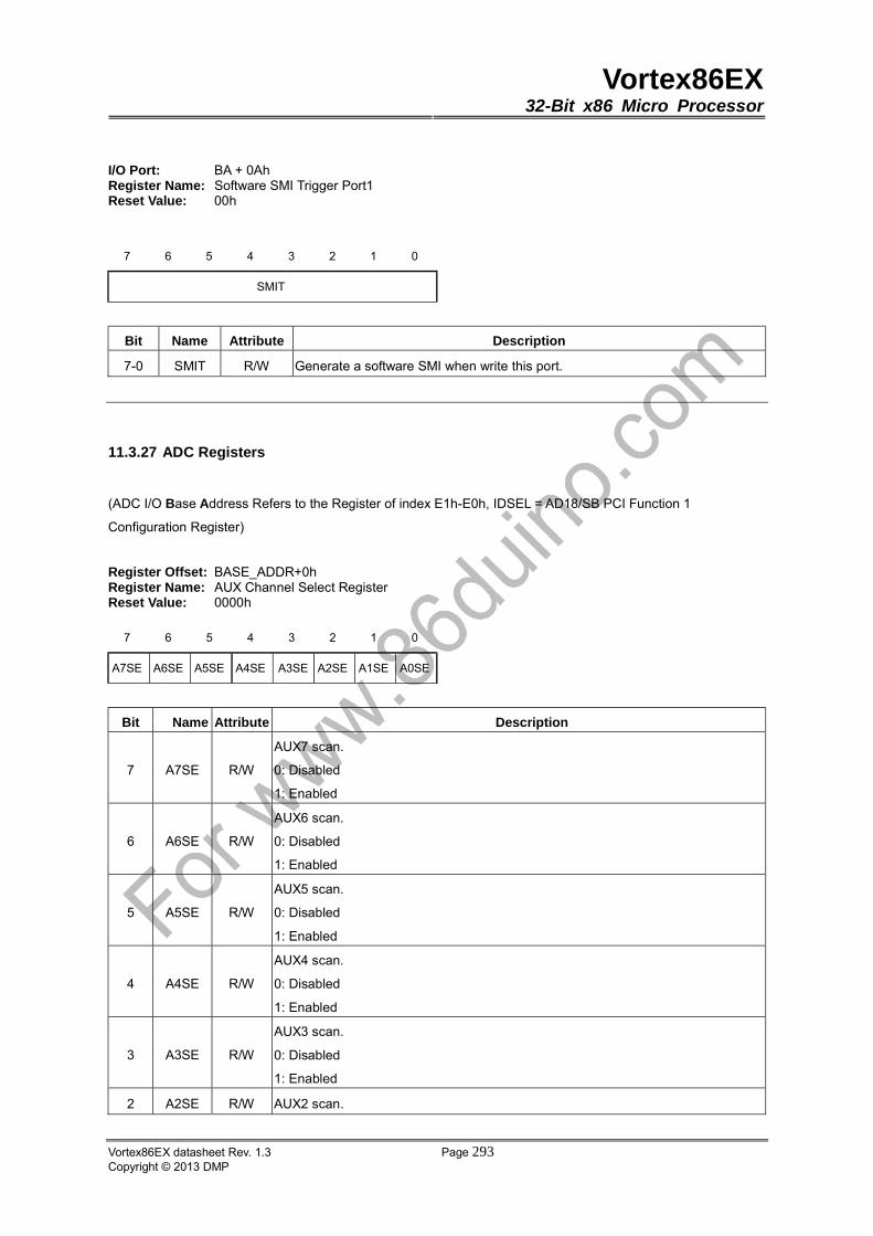
Vortex86EX32-Bit x86 Micro Processor
Vortex86EX datasheet Rev. 1.3 Page 293Copyright © 2013 DMP
I/O Port: BA + 0Ah Register Name: Software SMI Trigger Port1 Reset Value: 00h
7 6 5 4 3 2 1 0
SMIT
Bit Name Attribute Description
7-0 SMIT R/W Generate a software SMI when write this port.
11.3.27 ADC Registers
(ADC I/O Base Address Refers to the Register of index E1h-E0h, IDSEL = AD18/SB PCI Function 1
Configuration Register)
Register Offset: BASE_ADDR+0h Register Name: AUX Channel Select Register Reset Value: 0000h
7 6 5 4 3 2 1 0
A7SE A6SE A5SE A4SE A3SE A2SE A1SE A0SE
Bit Name Attribute Description
7 A7SE R/W
AUX7 scan.
0: Disabled
1: Enabled
6 A6SE R/W
AUX6 scan.
0: Disabled
1: Enabled
5 A5SE R/W
AUX5 scan.
0: Disabled
1: Enabled
4 A4SE R/W
AUX4 scan.
0: Disabled
1: Enabled
3 A3SE R/W
AUX3 scan.
0: Disabled
1: Enabled
2 A2SE R/W AUX2 scan.
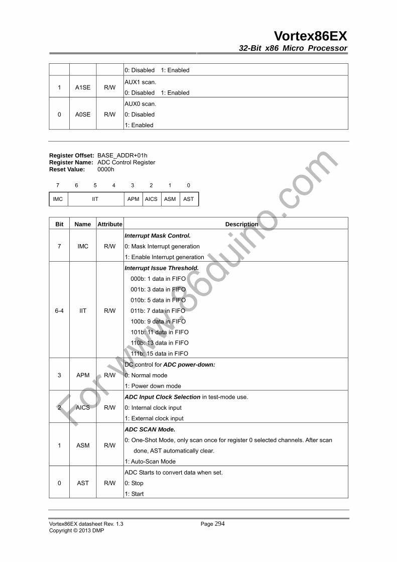
Vortex86EX32-Bit x86 Micro Processor
Vortex86EX datasheet Rev. 1.3 Page 294Copyright © 2013 DMP
0: Disabled 1: Enabled
1 A1SE R/W AUX1 scan.
0: Disabled 1: Enabled
0 A0SE R/W
AUX0 scan.
0: Disabled
1: Enabled
Register Offset: BASE_ADDR+01h Register Name: ADC Control Register Reset Value: 0000h
7 6 5 4 3 2 1 0
IMC IIT APM AICS ASM AST
Bit Name Attribute Description
7 IMC R/W
Interrupt Mask Control.
0: Mask Interrupt generation
1: Enable Interrupt generation
6-4 IIT R/W
Interrupt Issue Threshold.
000b: 1 data in FIFO
001b: 3 data in FIFO
010b: 5 data in FIFO
011b: 7 data in FIFO
100b: 9 data in FIFO
101b: 11 data in FIFO
110b: 13 data in FIFO
111b: 15 data in FIFO
3 APM R/W
DC control for ADC power-down:
0: Normal mode
1: Power down mode
2 AICS R/W
ADC Input Clock Selection in test-mode use.
0: Internal clock input
1: External clock input
1 ASM R/W
ADC SCAN Mode.
0: One-Shot Mode, only scan once for register 0 selected channels. After scan
done, AST automatically clear.
1: Auto-Scan Mode
0 AST R/W
ADC Starts to convert data when set.
0: Stop
1: Start

Vortex86EX32-Bit x86 Micro Processor
Vortex86EX datasheet Rev. 1.3 Page 295Copyright © 2013 DMP
Register Offset: BASE_ADDR+02h Register Name: ADC Status Register Reset Value: 0000h
7 6 5 4 3 2 1 0
IS RSVD DR
Bit Name Attribute Description
7 IS R/WCInterrupt Status. When FIFO data is matching IIT, this bit will be set. Write “1” to
clear
6-1 RSVD RO Reserved.
0 DR RO
Data Ready in FIFO.
0: Not Ready
1: Ready
Register Offset: BASE_ADDR+04h Register Name: ADC Data Register Reset Value: 0000h
15 14 13 12 11 10 9 8 7 6 5 4 3 2 1 0
AC RSVD AOD
Bit Name Attribute Description
15-13 AC RO Indicate AOD[10:0] belongs which AUX Channel
12-11 RSVD RO Reserved.
10-0 AOD RO ADC Output Data [10:0]. This data is ready during Register 2 bit0 DR is set. After
read data [10:0], Hardware will automatically clear DR..
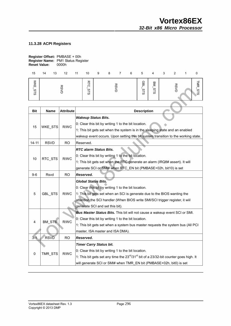
Vortex86EX32-Bit x86 Micro Processor
Vortex86EX datasheet Rev. 1.3 Page 296Copyright © 2013 DMP
11.3.28 ACPI Registers
Register Offset: PMBASE + 00h Register Name: PM1 Status Register Reset Value: 0000h
15 14 13 12 11 10 9 8 7 6 5 4 3 2 1 0
Bit Name Attribute Description
15 WKE_STS R/WC
Wakeup Status Bits.
0: Clear this bit by writing 1 to the bit location.
1: This bit gets set when the system is in the sleeping state and an enabled
wakeup event occurs. Upon setting this bit system transition to the working state.
14-11 RSVD RO Reserved.
10 RTC_STS R/WC
RTC alarm Status Bits.
0: Clear this bit by writing 1 to the bit location.
1: This bit gets set when the RTC generate an alarm (IRQ8# assert). It will
generate SCI or SMI# when RTC_EN bit (PMBASE+02h, bit10) is set
9-6 Rsvd RO Reserved.
5 GBL_STS R/WC
Global Status Bits.
0: Clear this bit by writing 1 to the bit location.
1: This bit gets set when an SCI is generate due to the BIOS wanting the
attention the SCI handler (When BIOS write SMI/SCI trigger register, it wiil
generate SCI and set this bit).
4 BM_STS R/WC
Bus Master Status Bits. This bit will not cause a wakeup event SCI or SMI.
0: Clear this bit by writing 1 to the bit location.
1: This bit gets set when a system bus master requests the system bus (All PCI
master, ISA master and ISA DMA).
3-1 RSVD RO Reserved.
0 TMR_STS R/WC
Timer Carry Status bit.
0: Clear this bit by writing 1 to the bit location.
1: This bit gets set any time the 23rd/31st bit of a 23/32-bit counter goes high. It
will generate SCI or SMI# when TMR_EN bit (PMBASE+02h, bit0) is set
Vortex86EX32-Bit x86 Micro Processor
Vortex86EX datasheet Rev. 1.3 Page 297Copyright © 2013 DMP
Register Offset: PMBASE + 02h Register Name: PM1 Enable Register Reset Value: 0000h
15 14 13 12 11 10 9 8 7 6 5 4 3 2 1 0
Bit Name Attribute Description
15-11 RSVD RO Reserved.
10 RTC_EN R/W RTC Alarm Enable bit. When both the RTC_EN bit and RTC_STS bit are set,
SCI/SMI# is raised.
9-6 RSVD RO Reserved.
5 GBL_EN R/W Global Enable bit. When both the GBL_EN bit and GBL_STS bit are set, an
SCI is raised.
4-1 RSVD RO Reserved.
0 TMR_EN R/W
Timer Carry Interrupt Enable bit. When this bit is set then an SCI or SMI
event is generated any time the TMR_STS bit is set. SCI_EN bit is at
PMBASE+04h, bit0.
TMR_EN SCI_EN Description
0 X No SMI# or SCI
1 0 SMI#
1 1 SCI
Register Offset: PMBASE + 04h Register Name: PM1 Control Register Reset Value: 0000h
15 14 13 12 11 10 9 8 7 6 5 4 3 2 1 0
Bit Name Attribute Description
15-14 RSVD RO Reserved.
13 SLP_EN WO Sleep Enable. Setting this bit causes the system to sequence into the sleeping
state associated with SLP_TYPx.
12-10 SLP_TYPx R/W
Defines the types of the sleeping state the system enters when SLP_EN bit is set
to one.
000b: Normal ON, typically maps to S0 state

Vortex86EX32-Bit x86 Micro Processor
Vortex86EX datasheet Rev. 1.3 Page 298Copyright © 2013 DMP
001b: Stop Processor clock, S1 state
010b: Suspend-to-RAM, S3 state
011b: Suspend-to-Disk, S4 state
100b: Soft Off, S5 state
101b-111b: reserved
9-3 RSVD RO Reserved.
2 GBL_RLS WO
Global Release. It is used by the ACPI software to raise an event to BIOS
software.
0: This bits always read as 0
1: ACPI write a 1 to this register to generate a SMI to pass execution control to
the BIOS when PMBASE+30h bit2 BIOS_SMI_EN set to one. The PMBASE+28h
bit2 BIOS_STS also set to indicate BIOS. When software clear BIOS_STS,
hardware also clear GBL_RLS.
1 BM_RLD R/W
Bus Master Reload.
0: Bus Master Request does not affect processor in the C3 state
1: Enable Bus Master Requests to cause processor in the C3 to transition to C0.
0 SCI_EN R/W
SCI Enable. Selects the power management event to be either an SCI or SMI for
PM1_STS bit10 (RTC Alarm).
0: Generate an SMI#
1: Generate an SCI
Register Offset: PMBASE + 08h Register Name: Power Management Timer Register Reset Value: 00000000h
31 30 29 28 27 26 25 24 23 22 21 20 19 18 17 16 15 14 13 12 11 10 9 8 7 6 5 4 3 2 1 0
Bit Name Attribute Description
31-24 E_TMR_VAL RO Reserved, must be 0 when on;y support 24bits timer.
23-0 TMR_VAL RO
Timer Value. It returns the running count of the power management timer in S0
state. This counter run off a 3.579545MHz clock (14.31818MHz/4). It is reset to
0 during a PCI reset and continues count until the 14.31818MHz is stopped.
Timer carry generates every 2.3435 seconds.

Vortex86EX32-Bit x86 Micro Processor
Vortex86EX datasheet Rev. 1.3 Page 299Copyright © 2013 DMP
Register Offset: PMBASE + 10h Register Name: Processor Control Register Reset Value: 00000000h
31 30 29 28 27 26 25 24 23 22 21 20 19 18 17 16 15 14 13 12 11 10 9 8 7 6 5 4 3 2 1 0
Bit Name Attribute Description
31-5 RSVD RO Reserved. (Possible locations of the clock throttling value)
4 THT_EN R/W
This bit enables clock throttling of clock as set in CLK_VAL field. THT_EN bit
must be 0 when changing CLK_VAL field.
0: Disabled
1: Enable CPU throttling
3-0 CLK_VAL R/W Possible locations for the clock throttling value when THT_EN set
Register Offset: PMBASE + 14h Register Name: Processor LVL2 Register Reset Value: 00h
7 6 5 4 3 2 1 0
P_LVL2
Bit Name Attribute Description
7-0 P_LVL2 RO
Read this register to return all 0; write to this register have no effect. Read to
this register also generate an “enter C2 power state” signal to hardware (clock
control logic).
Register Offset: PMBASE + 15h Register Name: Processor LVL3 Register Reset Value: 00h
7 6 5 4 3 2 1 0
P_LVL3
Bit Name Attribute Description
7-0 P_LVL3 RO
Read this register to return all 0; write to this register have no effect. Reads to
this register also generate an “enter C3 power state” signal to hardware (clock
control logic).
Vortex86EX32-Bit x86 Micro Processor
Vortex86EX datasheet Rev. 1.3 Page 300Copyright © 2013 DMP
Register Offset: PMBASE + 20h Register Name: GPE0_STS General Purpose Event 0 Status Register Reset Value: 00000000h
31 30 29 28 27 26 25 24 23 22 21 20 19 18 17 16 15 14 13 12 11 10 9 8 7 6 5 4 3 2 1 0
Bit Name Attribute Description
31-1 RSVD RO Reserved.
0 RSVD R/WC Reserved.
Register Offset: PMBASE + 24h Register Name: GPE0_EN General Purpose Event 0 Enable Register Reset Value: 00000000h
31 30 29 28 27 26 25 24 23 22 21 20 19 18 17 16 15 14 13 12 11 10 9 8 7 6 5 4 3 2 1 0
Bit Name Attribute Description
31 S_WKE R/W
S/W Wake Up Control.
Set ‘1’ will cause PMBase+0h bit15 WKE_STS to ‘1’.
Set ‘0’ will cause PMBase+0h bit15 WKE_STS to ‘0’.
After WKE_STS write one clear to 0, this bit also will clear to 0.
30-1 RSVD RO Reserved.
0 RSVD R/W
Reserved.
0: Disabled
1: Enable the corresponding event.

Vortex86EX32-Bit x86 Micro Processor
Vortex86EX datasheet Rev. 1.3 Page 301Copyright © 2013 DMP
Register Offset: PMBASE + 28h Register Name: GPE0_SMI General Purpose Event 0 SMI Enable Register Reset Value: 00000000h
31 30 29 28 27 26 25 24 23 22 21 20 19 18 17 16 15 14 13 12 11 10 9 8 7 6 5 4 3 2 1 0
Bit Name Attribute Description
31-1 RSVD RO Reserved.
0 RSVD R/W Reserved.
Register Offset: PMBASE + 2Ch Register Name: Global Status Register Reset Value: 00000000h
31 30 29 28 27 26 25 24 23 22 21 20 19 18 17 16 15 14 13 12 11 10 9 8 7 6 5 4 3 2 1 0
Bit Name Attribute Description
31-13 RSVD R/O Reserved.
12 WDT_STS R/WC WDT SMI Status. This bit will be set to 1 when WDT timeout and the timeout
event is SMI.
11-8 RSVD R/O Reserved.
7 SLP_STS R/WC
Sleep SMI Status. This bit will be set to 1 when write “1” to PMBASE+04h bit
13 SLP_EN. And if both PMBASE+28h bit7 SLP_SMI_EN=1 and SLP_EN are
set “1”, that will generate SMI# and SLP_STS will set “1”.
6 RSVD RO Reserved.
5 RSVD R/WC Reserved.
4 USB1E_STS R/WC Legacy USB1 EHCI SMI Status.
3 USB1O_ST
S R/WC Legacy USB1 OHCI SMI Status.
2 BIOS_STS R/WC BIOS Status. This bit is set when PMBASE+04h bit2 GBL_RLS=1. Normally
it indicates ACPI passed the control to BIOS. Write 1 to clear.
1 B2_STS R/WC I/O port B2h SMI Status. This bit is set when I/O port B2h is written. Write 1
to clear.
0 SOFT_STS R/WC Software SMI Status. This bit is set when PMBASE+36h is written. Write 1 to

Vortex86EX32-Bit x86 Micro Processor
Vortex86EX datasheet Rev. 1.3 Page 302Copyright © 2013 DMP
clear.
Register Offset: PMBASE + 30h Register Name: Global Enable Register Reset Value: 00000000h
31 30 29 28 27 26 25 24 23 22 21 20 19 18 17 16 15 14 13 12 11 10 9 8 7 6 5 4 3 2 1 0
Bit Name Attribute Description
31-13 RSVD R/O Reserved.
12 WDT_EN R/W 0: None
1: Enable SMI# generation when WDT timeout and the timeout event is SMI.
11-8 RSVD R/O Reserved.
7 SLP_SMI_E
N R/W
0: None
1: Enable SMI# generation when write “1” to PMBASE+04h bit 13 SLP_EN
and system will not transition to sleep state:
6 RSVD R/O Reserved.
5 RSVD R/W Reserved.
4 USB1E_SMI
_EN R/W
0: None
1: Enable SMI# generation when legacy USB1 EHCI event occurs :
3 USB1O_SMI
_EN R/W
0: None
1: Enable SMI# generation when legacy USB1 OHCI event occurs :
2 BIOS_SMI_
EN R/W
0: None
1: Enable SMI# generation when PM_BASE+04h bit2 is set :
1 B2h_SMI_E
N R/W
0: None, I/O port B2h disabled
1: Enable SMI# generation when I/O port B2h is written. (Enable I/O port
b2h):
0 SOFT_SMI_
EN R/W
0: None
1: Enable SMI# generation when SMI command register(PM_BASE+36h) is
written:
Vortex86EX32-Bit x86 Micro Processor
Vortex86EX datasheet Rev. 1.3 Page 303Copyright © 2013 DMP
Register Offset: PMBASE + 34h Register Name: Global Control Register Reset Value: 00000000h
15 14 13 12 11 10 9 8 7 6 5 4 3 2 1 0
Bit Name Attribute Description
15-1 RSVD R/O Reserved.
0 BIOS_RLS R/W
BIOS Release. BIOS software write “1” to this bit to generate one SCI event
(If PMBASE+2h bit5 GBL_EN=1). Upon setting this, hardware automatically
set PMBASE+0h bit5 GBL_STS. This bit will be automatically cleared by
hardware when GBL_STS bit cleared by software.
Register Offset: PMBASE + 36h Register Name: Software SMI Command Register Reset Value: 00h
7 6 5 4 3 2 1 0
P_LVL3
Bit Name Attribute Description
7-0 SMI_CMD R/W
Software SMI Command Register. Writing this register to set
PMBASE+2Ch bit0 SOFT_STS. If PM_BASE+30h bit0 SOFT_SMI_EN is
“1”, It generates a SMI event too.
Vortex86EX32-Bit x86 Micro Processor
Vortex86EX datasheet Rev. 1.3 Page 304Copyright © 2013 DMP
Advance Power Management I/O Control Port
I/O Port: 0B2h Register Name: Software SMI Trigger Port2 Reset Value: 00h
7 6 5 4 3 2 1 0
SMIT
Bit Name Attribute Description
7-0 SMIT R/W Generate a software SMI when write this port. This port is useful when
B2h_SMI_EN (PMBASE+30h [1]) set 1, it will generate SMI#.
I/O Port: 0B3h Register Name: Software SMI Port3 Reset Value: 00h
7 6 5 4 3 2 1 0
SMIT
Bit Name Attribute Description
7-0 SMIT R/W This is a scratchpad register and it’s no affected to any other register or
function.
11.3.29 CrossBar Config Registers
(Base Address Refers to the Register of index 65h-64h, SB Function0 PCI Configuration Register)
Register Offset: BASE + 0, 1, 2, …, 9 Register Name: RichIO Port 0, 1, 2, …, 9 Selection Reset Value: 00h
7 6 5 4 3 2 1 0
RSVD RIOPS
Bit Name Attribute Description
7-5 RSVD RO Reserved.
4-0 SFS R/W
Rich IO Port, Function selection.
function
00000b No Function
00001b MCM P0
00010b MCM P1
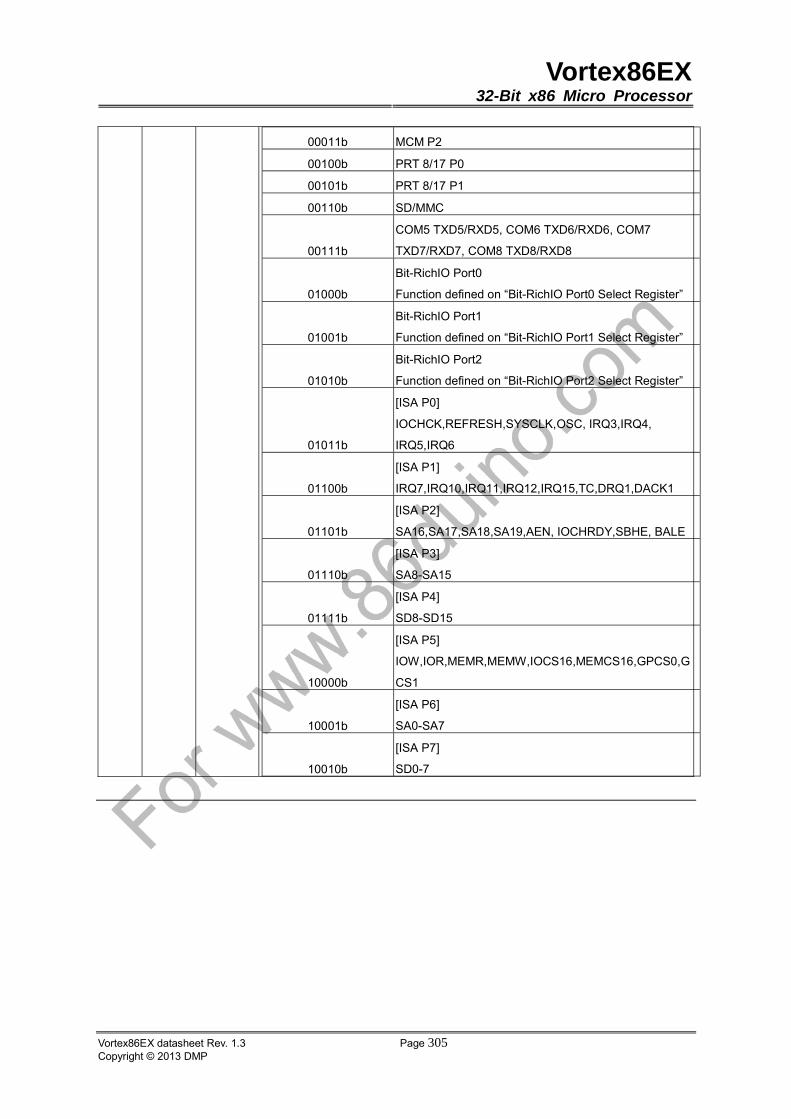
Vortex86EX32-Bit x86 Micro Processor
Vortex86EX datasheet Rev. 1.3 Page 305Copyright © 2013 DMP
00011b MCM P2
00100b PRT 8/17 P0
00101b PRT 8/17 P1
00110b SD/MMC
00111b
COM5 TXD5/RXD5, COM6 TXD6/RXD6, COM7
TXD7/RXD7, COM8 TXD8/RXD8
01000b
Bit-RichIO Port0
Function defined on “Bit-RichIO Port0 Select Register”
01001b
Bit-RichIO Port1
Function defined on “Bit-RichIO Port1 Select Register”
01010b
Bit-RichIO Port2
Function defined on “Bit-RichIO Port2 Select Register”
01011b
[ISA P0]
IOCHCK,REFRESH,SYSCLK,OSC, IRQ3,IRQ4,
IRQ5,IRQ6
01100b
[ISA P1]
IRQ7,IRQ10,IRQ11,IRQ12,IRQ15,TC,DRQ1,DACK1
01101b
[ISA P2]
SA16,SA17,SA18,SA19,AEN, IOCHRDY,SBHE, BALE
01110b
[ISA P3]
SA8-SA15
01111b
[ISA P4]
SD8-SD15
10000b
[ISA P5]
IOW,IOR,MEMR,MEMW,IOCS16,MEMCS16,GPCS0,G
CS1
10001b
[ISA P6]
SA0-SA7
10010b
[ISA P7]
SD0-7

Vortex86EX32-Bit x86 Micro Processor
Vortex86EX datasheet Rev. 1.3 Page 306Copyright © 2013 DMP
Register Offset: BASE + 10h, 11h, ..., 17h Register Name: Bit-RichIO Port0 Select Reset Value: 00h
7 6 5 4 3 2 1 0
RSVD BRIOPS
Bit Name Attribute Description
7-6 RSVD RO Reserved.
5-0 BRIOPS R/W
Bit Function selection for this bit:
(Some limitation need to take care for HDA, Full-duplex SPI and USB-Device in
below Note.)
function
000000b No Function
000001b COM1-TXD1
000010b COM1-RXD1
000011b COM2-TXD2
000100b COM2-RXD2
000101b COM3-TXD3
000110b COM3-RXD3
000111b COM4-TXD4
001000b COM4-RXD4
001001b SPI-CS1
001010b SPI-CLK
001011b SPI-DO
001100b SPI-DI
001101b I2C-SDA
001110b I2C-SCL
001111b CAN-TXD
010000b CAN-RXD
010001b USB-DEVICE+
010010b USB-DEVICE-
010011b KBDATA
010100b KBCLK
010101b MSDATA
010110b MSCLK
010111b LAN-LINK/ACK
011000b LAN-DUPLEX
011001b PRINT 1/17-PError

Vortex86EX32-Bit x86 Micro Processor
Vortex86EX datasheet Rev. 1.3 Page 307Copyright © 2013 DMP
011010b SPEAKER
011011b WDTOUT
011100b TXDEN1
011101b TXDEN2
011110b TXDEN3
011111b TXDEN4
100000b TXDEN5
100001b TXDEN6
100010b TXDEN7
100011b TXDEN8
100100b CLK-OUT
100101b MTBF
100110b SPI-CS2
100111b H_BCLK
101000b H_SYNC
101001b H_SDO
101010b H_SDI
101011b H_RST#
Note:
1. HDA
(H_BCLK, H_SYNC, H_SDO, H_SDI, H_RST#) must in the same
CrossBar Port.
H_BCLK must in CrossBar Port Bit [0]
H_SYNC must in CrossBar Port Bit [1]
H_SDO must in CrossBar Port Bit [2]
H_SDI must in CrossBar Port Bit [3]
H_RST# must in CrossBar Port Bit [4].
Full-Duplex SPI
(SPI_CS1, SPI_CLK, SPI_DI, SPI_DO, SPI_CS2) must in the same
CrossBar Port.
SPI_CS1 must in CrossBar Port Bit [0]
SPI_CLK must in CrossBar Port Bit [1]
SPI_DI must in CrossBar Port Bit [2]
SPI_DO must in CrossBar Port Bit [3]
SPI_CS2 must in CrossBar Port Bit [4]
USB Device
(USB-Device+, USB-Device-) must in the same CrossBar Port.
USB-Device+ must in CrossBar Port Bit [6]
USB-Device- must in CrossBar Port Bit [7]
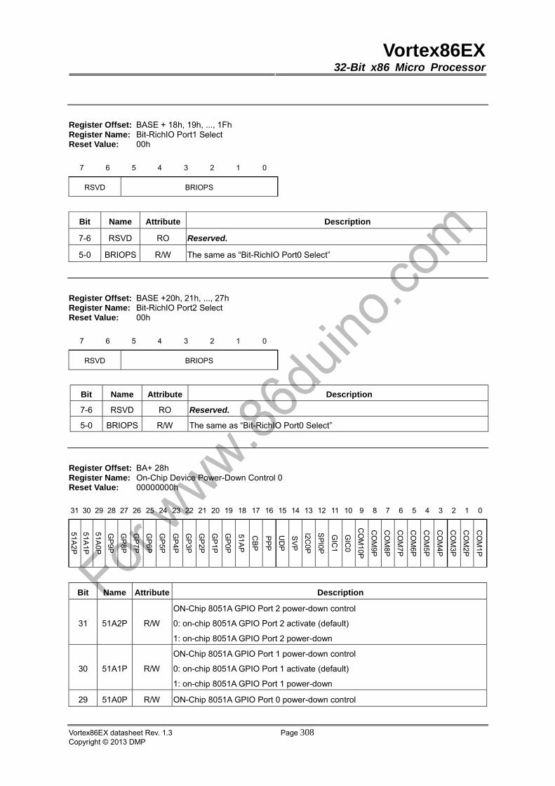
Vortex86EX32-Bit x86 Micro Processor
Vortex86EX datasheet Rev. 1.3 Page 308Copyright © 2013 DMP
Register Offset: BASE + 18h, 19h, ..., 1Fh Register Name: Bit-RichIO Port1 Select Reset Value: 00h
7 6 5 4 3 2 1 0
RSVD BRIOPS
Bit Name Attribute Description
7-6 RSVD RO Reserved.
5-0 BRIOPS R/W The same as “Bit-RichIO Port0 Select”
Register Offset: BASE +20h, 21h, ..., 27h Register Name: Bit-RichIO Port2 Select Reset Value: 00h
7 6 5 4 3 2 1 0
RSVD BRIOPS
Bit Name Attribute Description
7-6 RSVD RO Reserved.
5-0 BRIOPS R/W The same as “Bit-RichIO Port0 Select”
Register Offset: BA+ 28h Register Name: On-Chip Device Power-Down Control 0 Reset Value: 00000000h
31 30 29 28 27 26 25 24 23 22 21 20 19 18 17 16 15 14 13 12 11 10 9 8 7 6 5 4 3 2 1 0
Bit Name Attribute Description
31 51A2P R/W
ON-Chip 8051A GPIO Port 2 power-down control
0: on-chip 8051A GPIO Port 2 activate (default)
1: on-chip 8051A GPIO Port 2 power-down
30 51A1P R/W
ON-Chip 8051A GPIO Port 1 power-down control
0: on-chip 8051A GPIO Port 1 activate (default)
1: on-chip 8051A GPIO Port 1 power-down
29 51A0P R/W ON-Chip 8051A GPIO Port 0 power-down control
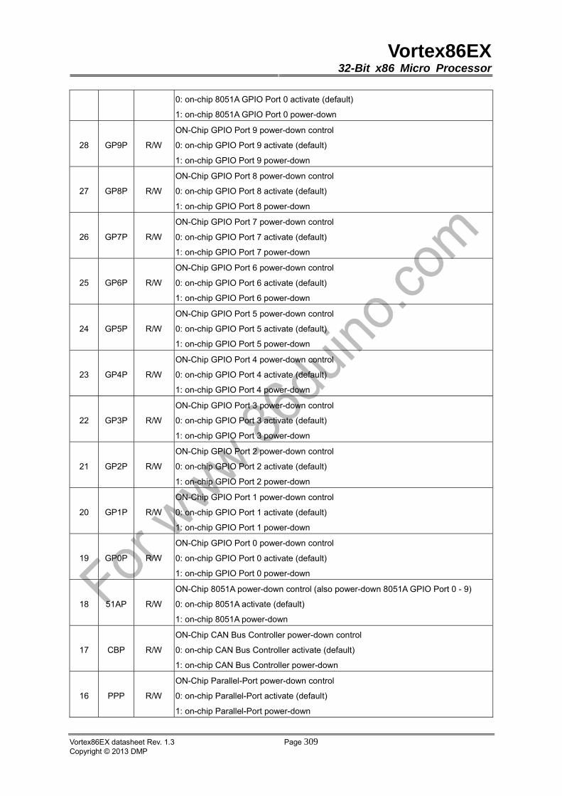
Vortex86EX32-Bit x86 Micro Processor
Vortex86EX datasheet Rev. 1.3 Page 309Copyright © 2013 DMP
0: on-chip 8051A GPIO Port 0 activate (default)
1: on-chip 8051A GPIO Port 0 power-down
28 GP9P R/W
ON-Chip GPIO Port 9 power-down control
0: on-chip GPIO Port 9 activate (default)
1: on-chip GPIO Port 9 power-down
27 GP8P R/W
ON-Chip GPIO Port 8 power-down control
0: on-chip GPIO Port 8 activate (default)
1: on-chip GPIO Port 8 power-down
26 GP7P R/W
ON-Chip GPIO Port 7 power-down control
0: on-chip GPIO Port 7 activate (default)
1: on-chip GPIO Port 7 power-down
25 GP6P R/W
ON-Chip GPIO Port 6 power-down control
0: on-chip GPIO Port 6 activate (default)
1: on-chip GPIO Port 6 power-down
24 GP5P R/W
ON-Chip GPIO Port 5 power-down control
0: on-chip GPIO Port 5 activate (default)
1: on-chip GPIO Port 5 power-down
23 GP4P R/W
ON-Chip GPIO Port 4 power-down control
0: on-chip GPIO Port 4 activate (default)
1: on-chip GPIO Port 4 power-down
22 GP3P R/W
ON-Chip GPIO Port 3 power-down control
0: on-chip GPIO Port 3 activate (default)
1: on-chip GPIO Port 3 power-down
21 GP2P R/W
ON-Chip GPIO Port 2 power-down control
0: on-chip GPIO Port 2 activate (default)
1: on-chip GPIO Port 2 power-down
20 GP1P R/W
ON-Chip GPIO Port 1 power-down control
0: on-chip GPIO Port 1 activate (default)
1: on-chip GPIO Port 1 power-down
19 GP0P R/W
ON-Chip GPIO Port 0 power-down control
0: on-chip GPIO Port 0 activate (default)
1: on-chip GPIO Port 0 power-down
18 51AP R/W
ON-Chip 8051A power-down control (also power-down 8051A GPIO Port 0 - 9)
0: on-chip 8051A activate (default)
1: on-chip 8051A power-down
17 CBP R/W
ON-Chip CAN Bus Controller power-down control
0: on-chip CAN Bus Controller activate (default)
1: on-chip CAN Bus Controller power-down
16 PPP R/W
ON-Chip Parallel-Port power-down control
0: on-chip Parallel-Port activate (default)
1: on-chip Parallel-Port power-down
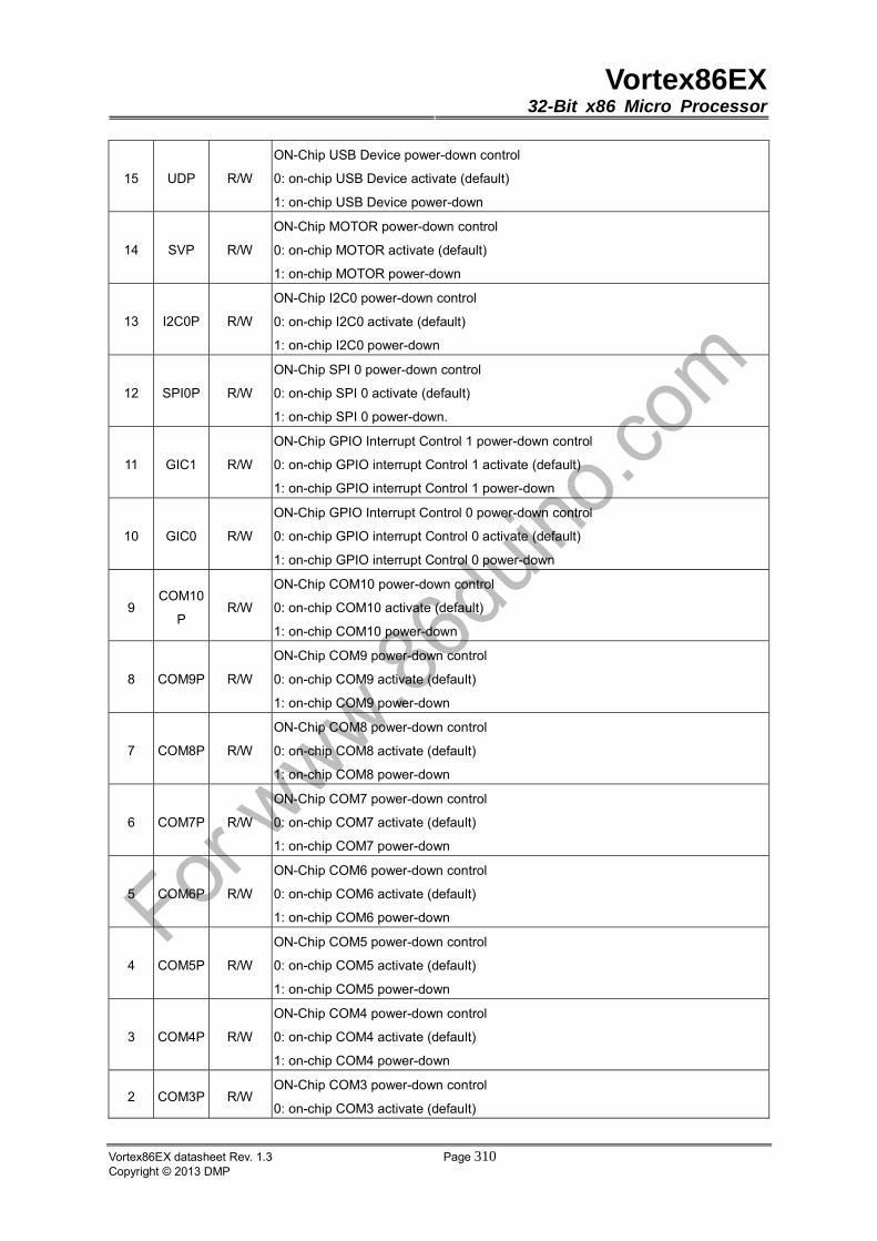
Vortex86EX32-Bit x86 Micro Processor
Vortex86EX datasheet Rev. 1.3 Page 310Copyright © 2013 DMP
15 UDP R/W
ON-Chip USB Device power-down control
0: on-chip USB Device activate (default)
1: on-chip USB Device power-down
14 SVP R/W
ON-Chip MOTOR power-down control
0: on-chip MOTOR activate (default)
1: on-chip MOTOR power-down
13 I2C0P R/W
ON-Chip I2C0 power-down control
0: on-chip I2C0 activate (default)
1: on-chip I2C0 power-down
12 SPI0P R/W
ON-Chip SPI 0 power-down control
0: on-chip SPI 0 activate (default)
1: on-chip SPI 0 power-down.
11 GIC1 R/W
ON-Chip GPIO Interrupt Control 1 power-down control
0: on-chip GPIO interrupt Control 1 activate (default)
1: on-chip GPIO interrupt Control 1 power-down
10 GIC0 R/W
ON-Chip GPIO Interrupt Control 0 power-down control
0: on-chip GPIO interrupt Control 0 activate (default)
1: on-chip GPIO interrupt Control 0 power-down
9 COM10
P R/W
ON-Chip COM10 power-down control
0: on-chip COM10 activate (default)
1: on-chip COM10 power-down
8 COM9P R/W
ON-Chip COM9 power-down control
0: on-chip COM9 activate (default)
1: on-chip COM9 power-down
7 COM8P R/W
ON-Chip COM8 power-down control
0: on-chip COM8 activate (default)
1: on-chip COM8 power-down
6 COM7P R/W
ON-Chip COM7 power-down control
0: on-chip COM7 activate (default)
1: on-chip COM7 power-down
5 COM6P R/W
ON-Chip COM6 power-down control
0: on-chip COM6 activate (default)
1: on-chip COM6 power-down
4 COM5P R/W
ON-Chip COM5 power-down control
0: on-chip COM5 activate (default)
1: on-chip COM5 power-down
3 COM4P R/W
ON-Chip COM4 power-down control
0: on-chip COM4 activate (default)
1: on-chip COM4 power-down
2 COM3P R/W ON-Chip COM3 power-down control
0: on-chip COM3 activate (default)
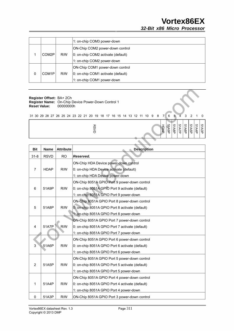
Vortex86EX32-Bit x86 Micro Processor
Vortex86EX datasheet Rev. 1.3 Page 311Copyright © 2013 DMP
1: on-chip COM3 power-down
1 COM2P R/W
ON-Chip COM2 power-down control
0: on-chip COM2 activate (default)
1: on-chip COM2 power-down
0 COM1P R/W
ON-Chip COM1 power-down control
0: on-chip COM1 activate (default)
1: on-chip COM1 power-down
Register Offset: BA+ 2Ch Register Name: On-Chip Device Power-Down Control 1 Reset Value: 00000000h
31 30 29 28 27 26 25 24 23 22 21 20 19 18 17 16 15 14 13 12 11 10 9 8 7 6 5 4 3 2 1 0
Bit Name Attribute Description
31-8 RSVD RO Reserved.
7 HDAP R/W
ON-Chip HDA Device power-down control
0: on-chip HDA Device activate (default)
1: on-chip HDA Device power-down
6 51A9P R/W
ON-Chip 8051A GPIO Port 9 power-down control
0: on-chip 8051A GPIO Port 9 activate (default)
1: on-chip 8051A GPIO Port 9 power-down
5 51A8P R/W
ON-Chip 8051A GPIO Port 8 power-down control
0: on-chip 8051A GPIO Port 8 activate (default)
1: on-chip 8051A GPIO Port 8 power-down
4 51A7P R/W
ON-Chip 8051A GPIO Port 7 power-down control
0: on-chip 8051A GPIO Port 7 activate (default)
1: on-chip 8051A GPIO Port 7 power-down
3 51A6P R/W
ON-Chip 8051A GPIO Port 6 power-down control
0: on-chip 8051A GPIO Port 6 activate (default)
1: on-chip 8051A GPIO Port 6 power-down
2 51A5P R/W
ON-Chip 8051A GPIO Port 5 power-down control
0: on-chip 8051A GPIO Port 5 activate (default)
1: on-chip 8051A GPIO Port 5 power-down
1 51A4P R/W
ON-Chip 8051A GPIO Port 4 power-down control
0: on-chip 8051A GPIO Port 4 activate (default)
1: on-chip 8051A GPIO Port 4 power-down
0 51A3P R/W ON-Chip 8051A GPIO Port 3 power-down control

Vortex86EX32-Bit x86 Micro Processor
Vortex86EX datasheet Rev. 1.3 Page 312Copyright © 2013 DMP
0: on-chip 8051A GPIO Port 3 activate (default)
1: on-chip 8051A GPIO Port 3 power-down
Register Offset: BA + 30h, 31h, ..., 7Fh Register Name: CrossBar PAD 0 – 79 Attribute Reset Value: 00h
7 6 5 4 3 2 1 0
RSVD PSR PST DCC ISC
Bit Name Attribute Description
7-5 RSVD RO Reserved.
4 PSR R/W
Pad Slew Rate Control.
0: low slew rate (default)
1: high slew rate
3 PST R/W
Pad Smitter Trigger Control.
0: Disable(default)
1: Enable
2 DCC R/W
Driving Current Control.
0: 8mA (default)
1: 16mA
1-0 ISC R/W
Input State Control.
00 : Tri-state
01: Pull-up
10: Pull-down
11: Reserved
Register Offset: BASE + 84h, 85h, ..., 89h Register Name: CrossBar-Port Group Selection, Port4, Port5, …, Port9 Reset Value: 00h
7 6 5 4 3 2 1 0
RSVD CPGS
Bit Name Attribute Description
7-5 RSVD RO Reserved.
4-0 CPGS R/W
Group selection for this port:
00000b: No Function
00001b: GPIO group
00010b: COM group
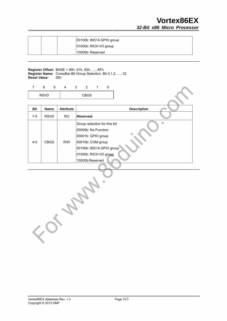
Vortex86EX32-Bit x86 Micro Processor
Vortex86EX datasheet Rev. 1.3 Page 313Copyright © 2013 DMP
00100b: 8051A GPIO group
01000b: RICH I/O group
10000b: Reserved
Register Offset: BASE + 90h, 91h, 92h, ...., AFh Register Name: CrossBar-Bit Group Selection, Bit 0,1,2, …, 32 Reset Value: 00h
7 6 5 4 3 2 1 0
RSVD CBGS
Bit Name Attribute Description
7-5 RSVD RO Reserved.
4-0 CBGS R/W
Group selection for this bit:
00000b: No Function
00001b: GPIO group
00010b: COM group
00100b: 8051A GPIO group
01000b: RICH I/O group
10000b:Reserved
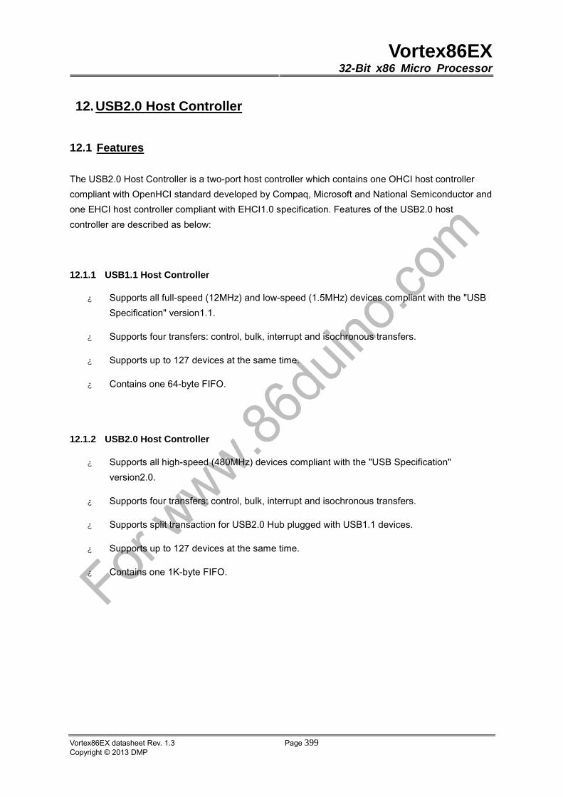
Vortex86EX32-Bit x86 Micro Processor
Vortex86EX datasheet Rev. 1.3 Page 399Copyright © 2013 DMP
12. USB2.0 Host Controller
12.1 Features
The USB2.0 Host Controller is a two-port host controller which contains one OHCI host controller
compliant with OpenHCI standard developed by Compaq, Microsoft and National Semiconductor and
one EHCI host controller compliant with EHCI1.0 specification. Features of the USB2.0 host
controller are described as below:
12.1.1 USB1.1 Host Controller
� Supports all full-speed (12MHz) and low-speed (1.5MHz) devices compliant with the "USB
Specification" version1.1.
� Supports four transfers: control, bulk, interrupt and isochronous transfers.
� Supports up to 127 devices at the same time.
� Contains one 64-byte FIFO.
12.1.2 USB2.0 Host Controller
� Supports all high-speed (480MHz) devices compliant with the "USB Specification"
version2.0.
� Supports four transfers: control, bulk, interrupt and isochronous transfers.
� Supports split transaction for USB2.0 Hub plugged with USB1.1 devices.
� Supports up to 127 devices at the same time.
� Contains one 1K-byte FIFO.
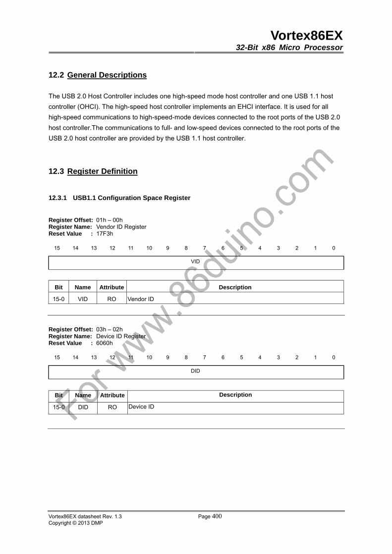
Vortex86EX32-Bit x86 Micro Processor
Vortex86EX datasheet Rev. 1.3 Page 400Copyright © 2013 DMP
12.2 General Descriptions
The USB 2.0 Host Controller includes one high-speed mode host controller and one USB 1.1 host
controller (OHCI). The high-speed host controller implements an EHCI interface. It is used for all
high-speed communications to high-speed-mode devices connected to the root ports of the USB 2.0
host controller.The communications to full- and low-speed devices connected to the root ports of the
USB 2.0 host controller are provided by the USB 1.1 host controller.
12.3 Register Definition
12.3.1 USB1.1 Configuration Space Register
Register Offset: 01h – 00h Register Name: Vendor ID Register Reset Value : 17F3h
15 14 13 12 11 10 9 8 7 6 5 4 3 2 1 0
VID
Bit Name Attribute Description
15-0 VID RO Vendor ID
Register Offset: 03h – 02h Register Name: Device ID Register Reset Value : 6060h
15 14 13 12 11 10 9 8 7 6 5 4 3 2 1 0
DID
Bit Name Attribute Description
15-0 DID RO Device ID
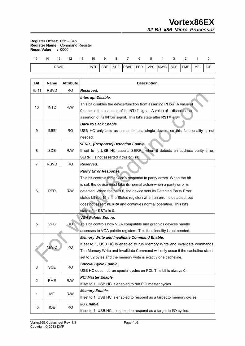
Vortex86EX32-Bit x86 Micro Processor
Vortex86EX datasheet Rev. 1.3 Page 401Copyright © 2013 DMP
Register Offset: 05h – 04h Register Name: Command Register Reset Value : 0000h
15 14 13 12 11 10 9 8 7 6 5 4 3 2 1 0
RSVD INTD BBE SDE RSVD PER VPS MWIC SCE PME ME IOE
Bit Name Attribute Description
15-11 RSVD RO Reserved.
10 INTD R/W
Interrupt Disable.
This bit disables the device/function from asserting INTx#. A value of
0 enables the assertion of its INTx# signal. A value of 1 disables the
assertion of its INTx# signal. This bit’s state after RST# is 0.
9 BBE RO
Back to Back Enable.
USB HC only acts as a master to a single device, so this functionality is not
needed.
8 SDE R/W
SERR_ (Response) Detection Enable.
If set to 1, USB HC asserts SERR_ when it detects an address parity error.
SERR_ is not asserted if this bit is 0.
7 RSVD RO Reserved.
6 PER R/W
Parity Error Response.
This bit controls the device's response to parity errors. When the bit
is set, the device must take its normal action when a parity error is
detected. When the bit is 0, the device sets its Detected Parity Error
status bit (bit 15 in the Status register) when an error is detected, but
does not assert PERR# and continues normal operation. This bit's
state after RST# is 0.
5 VPS RO
VGA Palette Snoop.
This bit controls how VGA compatible and graphics devices handle
accesses to VGA palette registers. This functionality is not needed.
4 MWIC RO
Memory Write and Invalidate Command Enable.
If set to 1, USB HC is enabled to run Memory Write and Invalidate commands.
The Memory Write and Invalidate Command will only occur if the cacheline size is
set to 32 bytes and the memory write is exactly one cacheline.
3 SCE RO Special Cycle Enable.
USB HC does not run special cycles on PCI. This bit is always 0.
2 PME R/W PCI Master Enable.
If set to 1, USB HC is enabled to run PCI master cycles.
1 ME R/W Memory Enable.
If set to 1, USB HC is enabled to respond as a target to memory cycles.
0 IOE RO I/O Enable.
If set to 1, USB HC is enabled to respond as a target to I/O cycles.
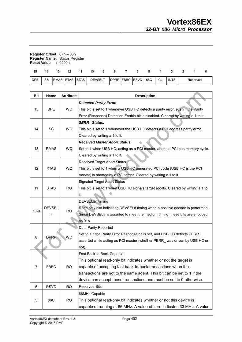
Vortex86EX32-Bit x86 Micro Processor
Vortex86EX datasheet Rev. 1.3 Page 402Copyright © 2013 DMP
Register Offset: 07h – 06h Register Name: Status Register Reset Value : 0200h
15 14 13 12 11 10 9 8 7 6 5 4 3 2 1 0
DPE SS RMAS RTAS STAS DEVSELT DPRP FBBC RSVD 66C CL INTS Reserved
Bit Name Attribute Description
15 DPE WC
Detected Parity Error.
This bit is set to 1 whenever USB HC detects a parity error, even if the Parity
Error (Response) Detection Enable bit is disabled. Cleared by writing a 1 to it.
14 SS WC
SERR_ Status.
This bit is set to 1 whenever the USB HC detects a PCI address parity error.
Cleared by writing a 1 to it.
13 RMAS WC
Received Master Abort Status.
Set to 1 when USB HC, acting as a PCI master, aborts a PCI bus memory cycle.
Cleared by writing a 1 to it.
12 RTAS WC
Received Target Abort Status
This bit is set to 1 when a USB HC generated PCI cycle (USB HC is the PCI
master) is aborted by a PCI target. Cleared by writing a 1 to it.
11 STAS RO
Signaled Target Abort Status
This bit is set to 1 when USB HC signals target aborts. Cleared by writing a 1 to
it.
10-9DEVSEL
T RO
DEVSEL#n timing
Read only bits indicating DEVSEL# timing when a positive decode is performed.
Since DEVSEL# is asserted to meet the medium timing, these bits are encoded
as 01b.
8 DPRP WC
Data Parity Reported
Set to 1 if the Parity Error Response bit is set, and USB HC detects PERR_
asserted while acting as PCI master (whether PERR_ was driven by USB HC or
not).
7 FBBC RO
Fast Back-to-Back Capable
This optional read-only bit indicates whether or not the target is
capable of accepting fast back-to-back transactions when the
transactions are not to the same agent. This bit can be set to 1 if the
device can accept these transactions and must be set to 0 otherwise.
6 RSVD RO Reserved Bits
5 66C RO
66MHz Capable
This optional read-only bit indicates whether or not this device is
capable of running at 66 MHz. A value of zero indicates 33 MHz. A value
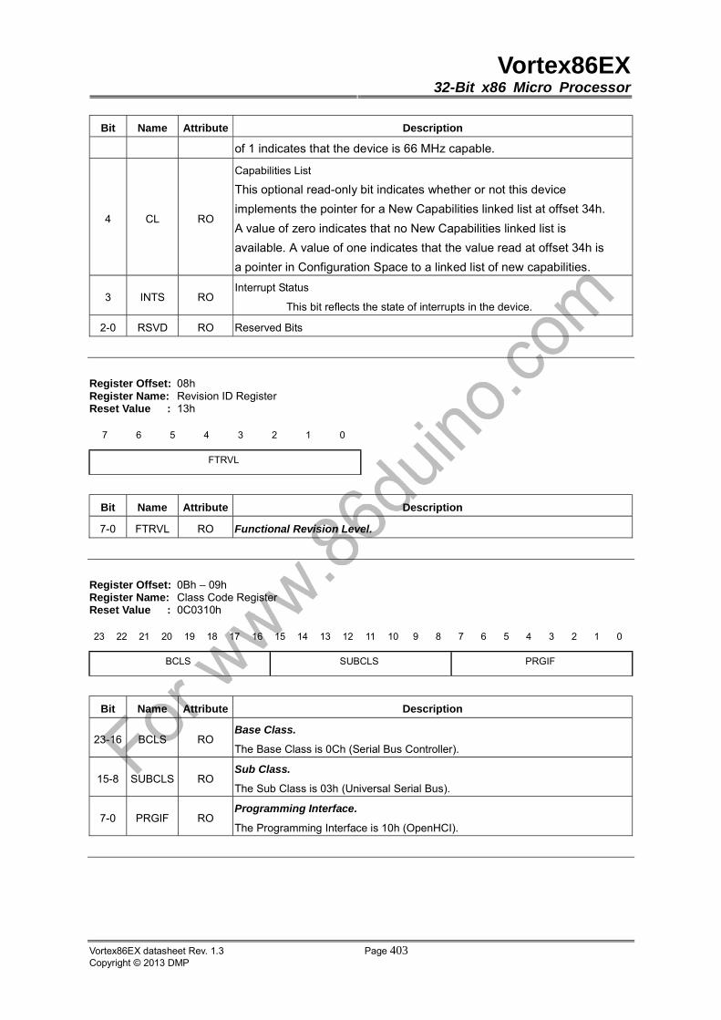
Vortex86EX32-Bit x86 Micro Processor
Vortex86EX datasheet Rev. 1.3 Page 403Copyright © 2013 DMP
Bit Name Attribute Description
of 1 indicates that the device is 66 MHz capable.
4 CL RO
Capabilities List
This optional read-only bit indicates whether or not this device
implements the pointer for a New Capabilities linked list at offset 34h.
A value of zero indicates that no New Capabilities linked list is
available. A value of one indicates that the value read at offset 34h is
a pointer in Configuration Space to a linked list of new capabilities.
3 INTS RO Interrupt Status
This bit reflects the state of interrupts in the device.
2-0 RSVD RO Reserved Bits
Register Offset: 08h Register Name: Revision ID Register Reset Value : 13h
7 6 5 4 3 2 1 0
FTRVL
Bit Name Attribute Description
7-0 FTRVL RO Functional Revision Level.
Register Offset: 0Bh – 09h Register Name: Class Code Register Reset Value : 0C0310h
23 22 21 20 19 18 17 16 15 14 13 12 11 10 9 8 7 6 5 4 3 2 1 0
BCLS SUBCLS PRGIF
Bit Name Attribute Description
23-16 BCLS RO Base Class.
The Base Class is 0Ch (Serial Bus Controller).
15-8 SUBCLS RO Sub Class.
The Sub Class is 03h (Universal Serial Bus).
7-0 PRGIF RO Programming Interface.
The Programming Interface is 10h (OpenHCI).
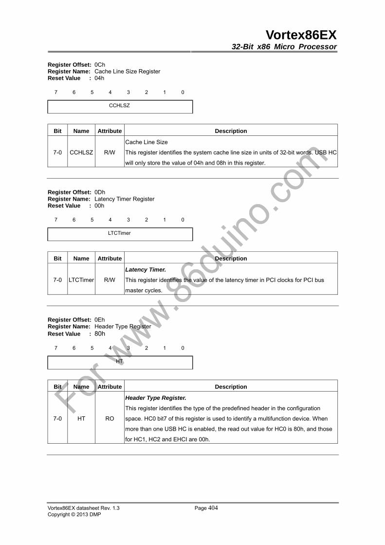
Vortex86EX32-Bit x86 Micro Processor
Vortex86EX datasheet Rev. 1.3 Page 404Copyright © 2013 DMP
Register Offset: 0Ch Register Name: Cache Line Size Register Reset Value : 04h
7 6 5 4 3 2 1 0
CCHLSZ
Bit Name Attribute Description
7-0 CCHLSZ R/W
Cache Line Size
This register identifies the system cache line size in units of 32-bit words. USB HC
will only store the value of 04h and 08h in this register.
Register Offset: 0Dh Register Name: Latency Timer Register Reset Value : 00h
7 6 5 4 3 2 1 0
LTCTimer
Bit Name Attribute Description
7-0 LTCTimer R/W
Latency Timer.
This register identifies the value of the latency timer in PCI clocks for PCI bus
master cycles.
Register Offset: 0Eh Register Name: Header Type Register Reset Value : 80h
7 6 5 4 3 2 1 0
HT
Bit Name Attribute Description
7-0 HT RO
Header Type Register.
This register identifies the type of the predefined header in the configuration
space. HC0 bit7 of this register is used to identify a multifunction device. When
more than one USB HC is enabled, the read out value for HC0 is 80h, and those
for HC1, HC2 and EHCI are 00h.

Vortex86EX32-Bit x86 Micro Processor
Vortex86EX datasheet Rev. 1.3 Page 405Copyright © 2013 DMP
Register Offset: 13h – 10h Register Name: Base Address Register Reset Value : 00000000h
31 30 29 28 27 26 25 24 23 22 21 20 19 18 17 16 15 14 13 12 11 10 9 8 7 6 5 4 3 2 1 0
BAD RSVD
Bit Name Attribute Description
31-12 BAD R/W Base Address.
POST writes the value of the memory base address to this register.
11-0 RSVD RO Reserved. These bits are always 0. It indicates a 4K-byte address range is
requested.
Register Offset: 2Dh – 2Ch Register Name: Subsystem Vendor ID Register Reset Value: 0000h
15 14 13 12 11 10 9 8 7 6 5 4 3 2 1 0
SVID
Bit Name Attribute Description
15-0 SVID RO This register contains the subsystem Vendor ID.
Register Offset: 2Fh – 2Eh Register Name: Subsystem Device ID Register Reset Value: 0000h
15 14 13 12 11 10 9 8 7 6 5 4 3 2 1 0
SDID
Bit Name Attribute Description
15-0 SDID RO This register contains the subsystem Device ID.
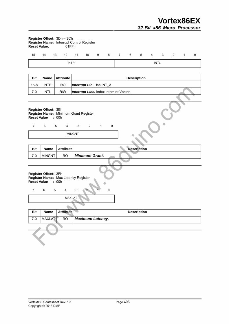
Vortex86EX32-Bit x86 Micro Processor
Vortex86EX datasheet Rev. 1.3 Page 406Copyright © 2013 DMP
Register Offset: 3Dh – 3Ch Register Name: Interrupt Control Register Reset Value: 01FFh
15 14 13 12 11 10 9 8 7 6 5 4 3 2 1 0
INTP INTL
Bit Name Attribute Description
15-8 INTP RO Interrupt Pin. Use INT_A.
7-0 INTL R/W Interrupt Line. Index Interrupt Vector.
Register Offset: 3Eh Register Name: Minimum Grant Register Reset Value : 00h
7 6 5 4 3 2 1 0
MINGNT
Bit Name Attribute Description
7-0 MINGNT RO Minimum Grant.
Register Offset: 3Fh Register Name: Max Latency Register Reset Value : 00h
7 6 5 4 3 2 1 0
MAXLAT
Bit Name Attribute Description
7-0 MAXLAT RO Maximum Latency.

Vortex86EX32-Bit x86 Micro Processor
Vortex86EX datasheet Rev. 1.3 Page 407Copyright © 2013 DMP
Register Offset: 43h – 40h Register Name: Reserved
Register Offset: 47h – 44h Register Name: Reserved
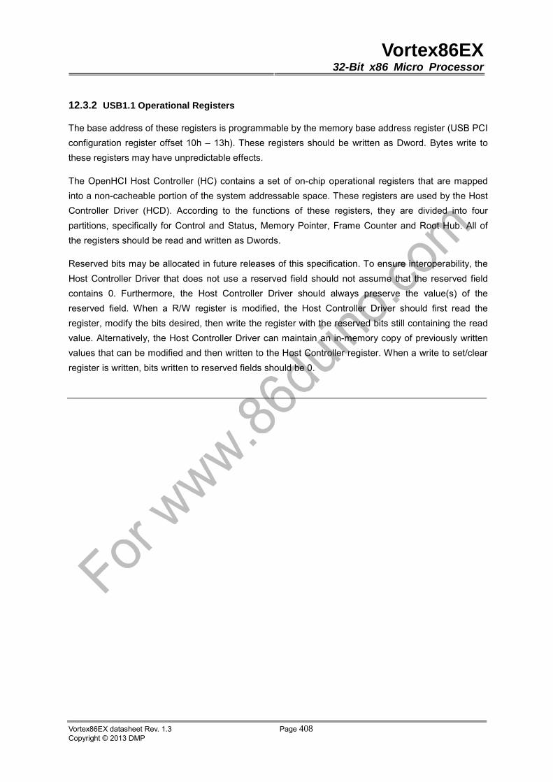
Vortex86EX32-Bit x86 Micro Processor
Vortex86EX datasheet Rev. 1.3 Page 408Copyright © 2013 DMP
12.3.2 USB1.1 Operational Registers
The base address of these registers is programmable by the memory base address register (USB PCI
configuration register offset 10h – 13h). These registers should be written as Dword. Bytes write to
these registers may have unpredictable effects.
The OpenHCI Host Controller (HC) contains a set of on-chip operational registers that are mapped
into a non-cacheable portion of the system addressable space. These registers are used by the Host
Controller Driver (HCD). According to the functions of these registers, they are divided into four
partitions, specifically for Control and Status, Memory Pointer, Frame Counter and Root Hub. All of
the registers should be read and written as Dwords.
Reserved bits may be allocated in future releases of this specification. To ensure interoperability, the
Host Controller Driver that does not use a reserved field should not assume that the reserved field
contains 0. Furthermore, the Host Controller Driver should always preserve the value(s) of the
reserved field. When a R/W register is modified, the Host Controller Driver should first read the
register, modify the bits desired, then write the register with the reserved bits still containing the read
value. Alternatively, the Host Controller Driver can maintain an in-memory copy of previously written
values that can be modified and then written to the Host Controller register. When a write to set/clear
register is written, bits written to reserved fields should be 0.
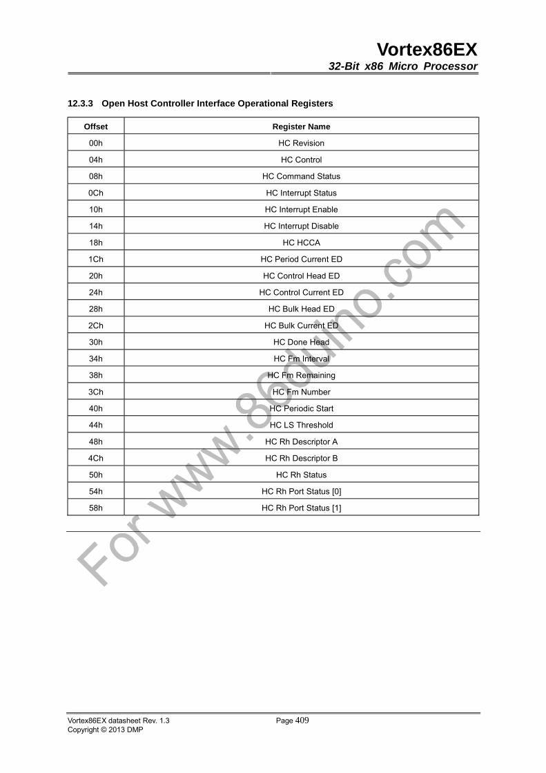
Vortex86EX32-Bit x86 Micro Processor
Vortex86EX datasheet Rev. 1.3 Page 409Copyright © 2013 DMP
12.3.3 Open Host Controller Interface Operational Registers
Offset Register Name
00h HC Revision
04h HC Control
08h HC Command Status
0Ch HC Interrupt Status
10h HC Interrupt Enable
14h HC Interrupt Disable
18h HC HCCA
1Ch HC Period Current ED
20h HC Control Head ED
24h HC Control Current ED
28h HC Bulk Head ED
2Ch HC Bulk Current ED
30h HC Done Head
34h HC Fm Interval
38h HC Fm Remaining
3Ch HC Fm Number
40h HC Periodic Start
44h HC LS Threshold
48h HC Rh Descriptor A
4Ch HC Rh Descriptor B
50h HC Rh Status
54h HC Rh Port Status [0]
58h HC Rh Port Status [1]
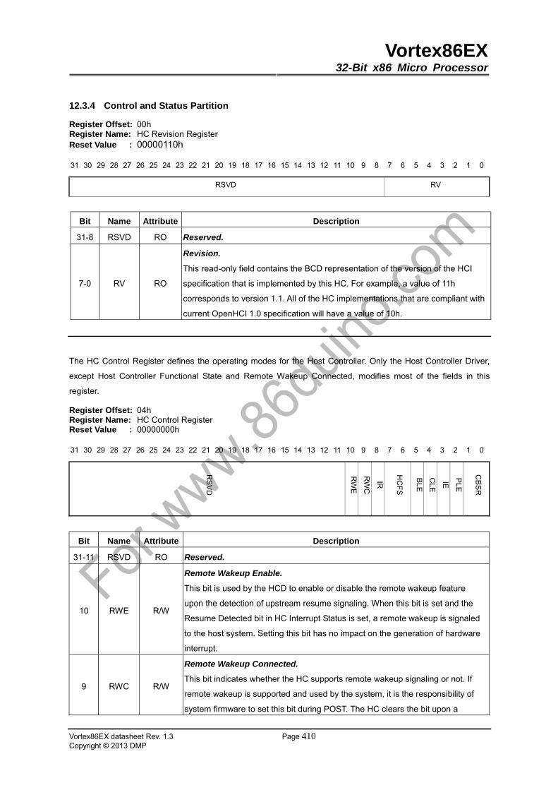
Vortex86EX32-Bit x86 Micro Processor
Vortex86EX datasheet Rev. 1.3 Page 410Copyright © 2013 DMP
12.3.4 Control and Status Partition
Register Offset: 00h Register Name: HC Revision Register Reset Value : 00000110h
31 30 29 28 27 26 25 24 23 22 21 20 19 18 17 16 15 14 13 12 11 10 9 8 7 6 5 4 3 2 1 0
RSVD RV
Bit Name Attribute Description
31-8 RSVD RO Reserved.
7-0 RV RO
Revision.
This read-only field contains the BCD representation of the version of the HCI
specification that is implemented by this HC. For example, a value of 11h
corresponds to version 1.1. All of the HC implementations that are compliant with
current OpenHCI 1.0 specification will have a value of 10h.
The HC Control Register defines the operating modes for the Host Controller. Only the Host Controller Driver,
except Host Controller Functional State and Remote Wakeup Connected, modifies most of the fields in this
register.
Register Offset: 04h Register Name: HC Control Register Reset Value : 00000000h
31 30 29 28 27 26 25 24 23 22 21 20 19 18 17 16 15 14 13 12 11 10 9 8 7 6 5 4 3 2 1 0
Bit Name Attribute Description
31-11 RSVD RO Reserved.
10 RWE R/W
Remote Wakeup Enable.
This bit is used by the HCD to enable or disable the remote wakeup feature
upon the detection of upstream resume signaling. When this bit is set and the
Resume Detected bit in HC Interrupt Status is set, a remote wakeup is signaled
to the host system. Setting this bit has no impact on the generation of hardware
interrupt.
9 RWC R/W
Remote Wakeup Connected.
This bit indicates whether the HC supports remote wakeup signaling or not. If
remote wakeup is supported and used by the system, it is the responsibility of
system firmware to set this bit during POST. The HC clears the bit upon a
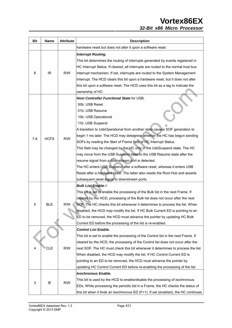
Vortex86EX32-Bit x86 Micro Processor
Vortex86EX datasheet Rev. 1.3 Page 411Copyright © 2013 DMP
Bit Name Attribute Description
hardware reset but does not alter it upon a software reset.
8 IR R/W
Interrupt Routing.
This bit determines the routing of interrupts generated by events registered in
HC Interrupt Status. If cleared, all interrupts are routed to the normal host bus
interrupt mechanism. If set, interrupts are routed to the System Management
Interrupt. The HCD clears this bit upon a hardware reset, but it does not alter
this bit upon a software reset. The HCD uses this bit as a tag to indicate the
ownership of HC.
7-6 HCFS R/W
Host Controller Functional State for USB.
00b: USB Reset
01b: USB Resume
10b: USB Operational
11b: USB Suspend
A transition to UsbOperational from another state causes SOF generation to
begin 1 ms later. The HCD may determine whether the HC has begun sending
SOFs by reading the Start of Frame field of HC Interrupt Status.
This field may be changed by the HC only in the UsbSuspend state. The HC
may move from the USB Suspend state to the USB Resume state after the
resume signal from a downstream port is detected.
The HC enters USB Suspend after a software reset, whereas it enters USB
Reset after a hardware reset. The latter also resets the Root Hub and asserts
subsequent reset signal to downstream ports.
5 BLE R/W
Bulk List Enable.
This bit is set to enable the processing of the Bulk list in the next Frame. If
cleared by the HCD, processing of the Bulk list does not occur after the next
SOF. The HC checks this bit whenever it determines to process the list. When
disabled, the HCD may modify the list. If HC Bulk Current ED is pointing to an
ED to be removed, the HCD must advance the pointer by updating HC Bulk
Current ED before the processing of the list is re-enabled.
4 CLE R/W
Control List Enable.
This bit is set to enable the processing of the Control list in the next Frame. If
cleared by the HCD, the processing of the Control list does not occur after the
next SOF. The HC must check this bit whenever it determines to process the list.
When disabled, the HCD may modify the list. If HC Control Current ED is
pointing to an ED to be removed, the HCD must advance the pointer by
updating HC Control Current ED before re-enabling the processing of the list.
3 IE R/W
Isochronous Enable.
This bit is used by the HCD to enable/disable the processing of isochronous
EDs. While processing the periodic list in a Frame, the HC checks the status of
this bit when it finds an Isochronous ED (F=1). If set (enabled), the HC continues
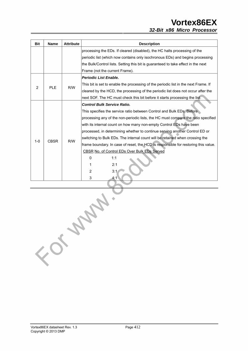
Vortex86EX32-Bit x86 Micro Processor
Vortex86EX datasheet Rev. 1.3 Page 412Copyright © 2013 DMP
Bit Name Attribute Description
processing the EDs. If cleared (disabled), the HC halts processing of the
periodic list (which now contains only isochronous EDs) and begins processing
the Bulk/Control lists. Setting this bit is guaranteed to take effect in the next
Frame (not the current Frame).
2 PLE R/W
Periodic List Enable.
This bit is set to enable the processing of the periodic list in the next Frame. If
cleared by the HCD, the processing of the periodic list does not occur after the
next SOF. The HC must check this bit before it starts processing the list.
1-0 CBSR R/W
Control Bulk Service Ratio.
This specifies the service ratio between Control and Bulk EDs. Before
processing any of the non-periodic lists, the HC must compare the ratio specified
with its internal count on how many non-empty Control EDs have been
processed, in determining whether to continue serving another Control ED or
switching to Bulk EDs. The internal count will be retained when crossing the
frame boundary. In case of reset, the HCD is responsible for restoring this value.
CBSR No. of Control EDs Over Bulk EDs Served
0 1:1
1 2:1
2 3:1
3 4:1
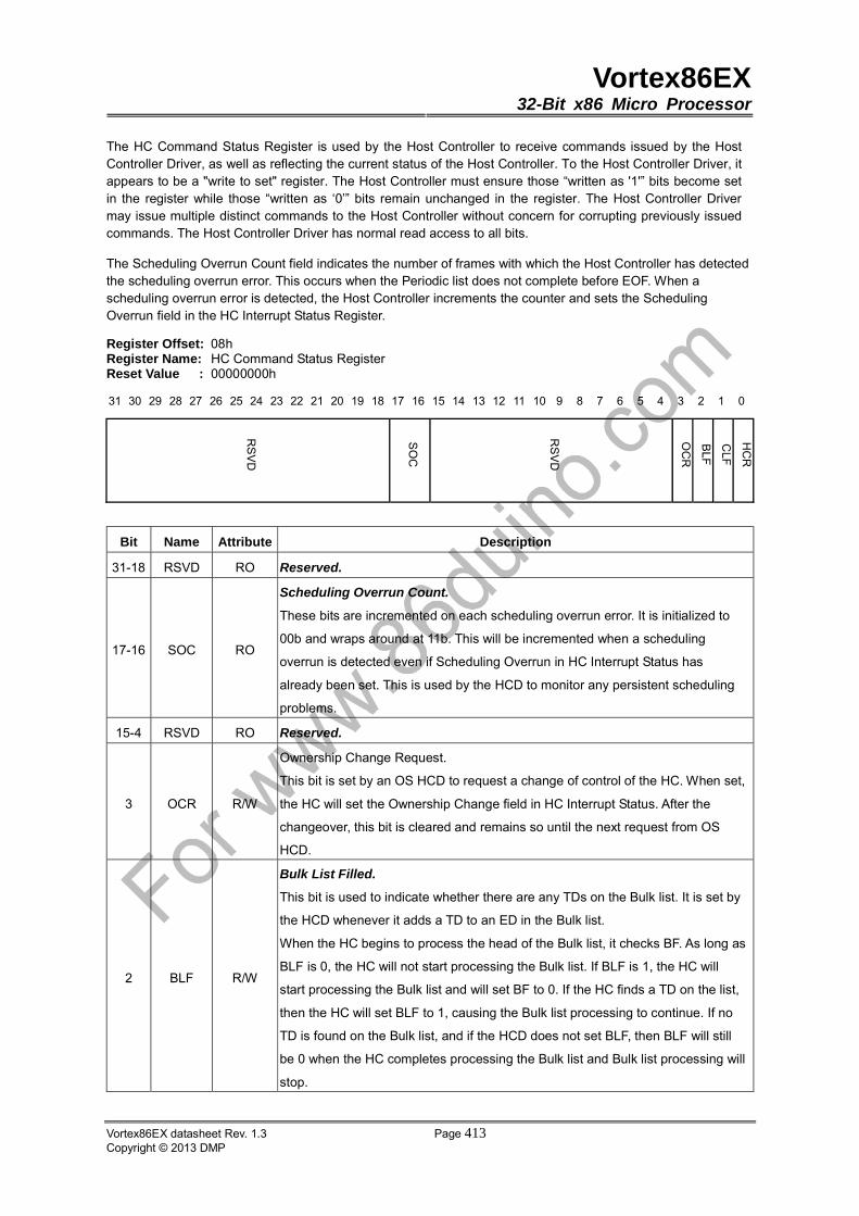
Vortex86EX32-Bit x86 Micro Processor
Vortex86EX datasheet Rev. 1.3 Page 413Copyright © 2013 DMP
The HC Command Status Register is used by the Host Controller to receive commands issued by the Host Controller Driver, as well as reflecting the current status of the Host Controller. To the Host Controller Driver, it appears to be a "write to set" register. The Host Controller must ensure those “written as '1'” bits become set in the register while those “written as ‘0’” bits remain unchanged in the register. The Host Controller Driver may issue multiple distinct commands to the Host Controller without concern for corrupting previously issued commands. The Host Controller Driver has normal read access to all bits.
The Scheduling Overrun Count field indicates the number of frames with which the Host Controller has detected the scheduling overrun error. This occurs when the Periodic list does not complete before EOF. When a scheduling overrun error is detected, the Host Controller increments the counter and sets the Scheduling Overrun field in the HC Interrupt Status Register.
Register Offset: 08h Register Name: HC Command Status Register Reset Value : 00000000h
31 30 29 28 27 26 25 24 23 22 21 20 19 18 17 16 15 14 13 12 11 10 9 8 7 6 5 4 3 2 1 0
Bit Name Attribute Description
31-18 RSVD RO Reserved.
17-16 SOC RO
Scheduling Overrun Count.
These bits are incremented on each scheduling overrun error. It is initialized to
00b and wraps around at 11b. This will be incremented when a scheduling
overrun is detected even if Scheduling Overrun in HC Interrupt Status has
already been set. This is used by the HCD to monitor any persistent scheduling
problems.
15-4 RSVD RO Reserved.
3 OCR R/W
Ownership Change Request.
This bit is set by an OS HCD to request a change of control of the HC. When set,
the HC will set the Ownership Change field in HC Interrupt Status. After the
changeover, this bit is cleared and remains so until the next request from OS
HCD.
2 BLF R/W
Bulk List Filled.
This bit is used to indicate whether there are any TDs on the Bulk list. It is set by
the HCD whenever it adds a TD to an ED in the Bulk list.
When the HC begins to process the head of the Bulk list, it checks BF. As long as
BLF is 0, the HC will not start processing the Bulk list. If BLF is 1, the HC will
start processing the Bulk list and will set BF to 0. If the HC finds a TD on the list,
then the HC will set BLF to 1, causing the Bulk list processing to continue. If no
TD is found on the Bulk list, and if the HCD does not set BLF, then BLF will still
be 0 when the HC completes processing the Bulk list and Bulk list processing will
stop.
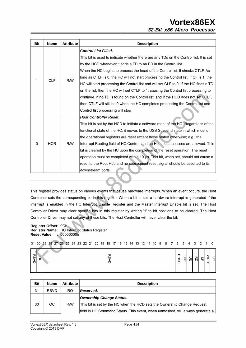
Vortex86EX32-Bit x86 Micro Processor
Vortex86EX datasheet Rev. 1.3 Page 414Copyright © 2013 DMP
Bit Name Attribute Description
1 CLF R/W
Control List Filled.
This bit is used to indicate whether there are any TDs on the Control list. It is set
by the HCD whenever it adds a TD to an ED in the Control list.
When the HC begins to process the head of the Control list, it checks CTLF. As
long as CTLF is 0, the HC will not start processing the Control list. If CF is 1, the
HC will start processing the Control list and will set CLF to 0. If the HC finds a TD
on the list, then the HC will set CTLF to 1, causing the Control list processing to
continue. If no TD is found on the Control list, and if the HCD does not set CTLF,
then CTLF will still be 0 when the HC completes processing the Control list and
Control list processing will stop
0 HCR R/W
Host Controller Reset.
This bit is set by the HCD to initiate a software reset of the HC. Regardless of the
functional state of the HC, it moves to the USB Suspend state in which most of
the operational registers are reset except those stated otherwise; e.g., the
Interrupt Routing field of HC Control, and no Host bus accesses are allowed. This
bit is cleared by the HC upon the completion of the reset operation. The reset
operation must be completed within 10 �s. This bit, when set, should not cause a
reset to the Root Hub and no subsequent reset signal should be asserted to its
downstream ports.
This register provides status on various events that cause hardware interrupts. When an event occurs, the Host
Controller sets the corresponding bit in this register. When a bit is set, a hardware interrupt is generated if the
interrupt is enabled in the HC Interrupt Enable Register and the Master Interrupt Enable bit is set. The Host
Controller Driver may clear specific bits in this register by writing '1' to bit positions to be cleared. The Host
Controller Driver may not set any of these bits. The Host Controller will never clear the bit.
Register Offset: 0Ch Register Name: HC Interrupt Status Register Reset Value : 00000000h
31 30 29 28 27 26 25 24 23 22 21 20 19 18 17 16 15 14 13 12 11 10 9 8 7 6 5 4 3 2 1 0
Bit Name Attribute Description
31 RSVD RO Reserved.
30 OC R/W
Ownership Change Status.
This bit is set by the HC when the HCD sets the Ownership Change Request
field in HC Command Status. This event, when unmasked, will always generate a

Vortex86EX32-Bit x86 Micro Processor
Vortex86EX datasheet Rev. 1.3 Page 415Copyright © 2013 DMP
Bit Name Attribute Description
System Management Interrupt (SMI_) immediately.
29-7 RSVD RO Reserved.
6 RHSC R/W
Root Hub Status Change Status.
This bit is set when the contents of HC Rh Status or the contents of any of HC Rh
Port Status [Number of Downstream Port] have changed.
5 FNO R/W
Frame Number Overflow Status.
This bit is set when the MSb of HC Fm Number (bit 15) changes values, from 0
to 1 or from 1 to 0, and after HCCA Frame Number has been updated.
4 UE R/W
Unrecoverable Error.
This bit is set when HC detects a system error not related to USB. HC
should not proceed with any processing nor signaling before the system
error has been corrected. HCD clears this bit after HC has been reset.
3 RD R/W
Resume Detected Status.
This bit is set when the HC detects that a device on the USB is asserting resume
signaling. It is the transition from no resume signaling to resume signaling
causing this bit to be set. This bit is not set when the HCD sets the USB
Resume state.
2 SF R/W
Start of Frame Status.
This bit is set by the HC at each start of a frame and after the update of HCCA
Frame Number. The HC also generates an SOF token at the same time.
1 WDH R/W
Write Back Done Head Status.
This bit is set immediately after the HC has written HC Done Head to HCCA
Done Head. Further updates of the HCCA Done Head will not occur until this bit
has been cleared. The HCD should only clear this bit after it has saved the
contents of HCCA Done Head.
0 SO R/W
Scheduling Overrun Status.
This bit is set when the USB schedule for the current Frame overruns and after
the update of HCCA Frame Number. A scheduling overrun will also cause the
Scheduling Overrun Count of HC Command Status to be incremented.

Vortex86EX32-Bit x86 Micro Processor
Vortex86EX datasheet Rev. 1.3 Page 416Copyright © 2013 DMP
Each enabled bit in the HcInterruptEnable register corresponds to an associated interrupt bit in the HC Interrupt
Status Register. The HC Interrupt Enable Register is used to control those events to generate a hardware
interrupt. When a bit is set in the HC Interrupt Status Register and the corresponding bit in the HC Interrupt
Enable Register is set and the Master Interrupt Enable bit is set, a hardware interrupt is requested on the host
bus.
Writing a '1' to a bit in this register sets the corresponding bit, whereas writing a '0' to a bit in this register leaves
the corresponding bit unchanged. On read, the current value of this register is returned.
Register Offset: 10h Register Name: HC Interrupt Enable Register Reset Value : 00000000h
31 30 29 28 27 26 25 24 23 22 21 20 19 18 17 16 15 14 13 12 11 10 9 8 7 6 5 4 3 2 1 0
Bit Name Attribute Description
31 MINTEn R/W
Master Interrupt Enable.
A '0' written to this field is ignored by the HC. A '1' written to this field enables
interrupt generation due to events specified in the other bits of this register. This is
used by the HCD as a Master Interrupt Enable.
30 ONCEn R/W
Ownership Change Enable.
0: Ignore.
1: Enabled interrupt generation due to Ownership Change.
29-7 RSVD RO Reserved.
6 RHSCEn R/W
Root Hub StatusChange Enable.
0: Ignore.
1: Enabled interrupt generation due to Root Hub Status Change.
5 FNOFEn R/W
Frame Number Overflow Enable.
0: Ignore.
1: Enabled interrupt generation due to Frame Number Overflow.
4 UE R/W
Unrecoverable Error Enable
0: Ignore
1: Enabled interrupt generation due to Unrecoverable Error.
3 RSDEn R/W
Resume Detected Enable.
0: Ignore.
1: Enabled interrupt generation due to Resume Detect.
2 SFEn R/W
Start of Frame Enable.
0: Ignore.
1: Enabled interrupt generation due to Start of Frame.
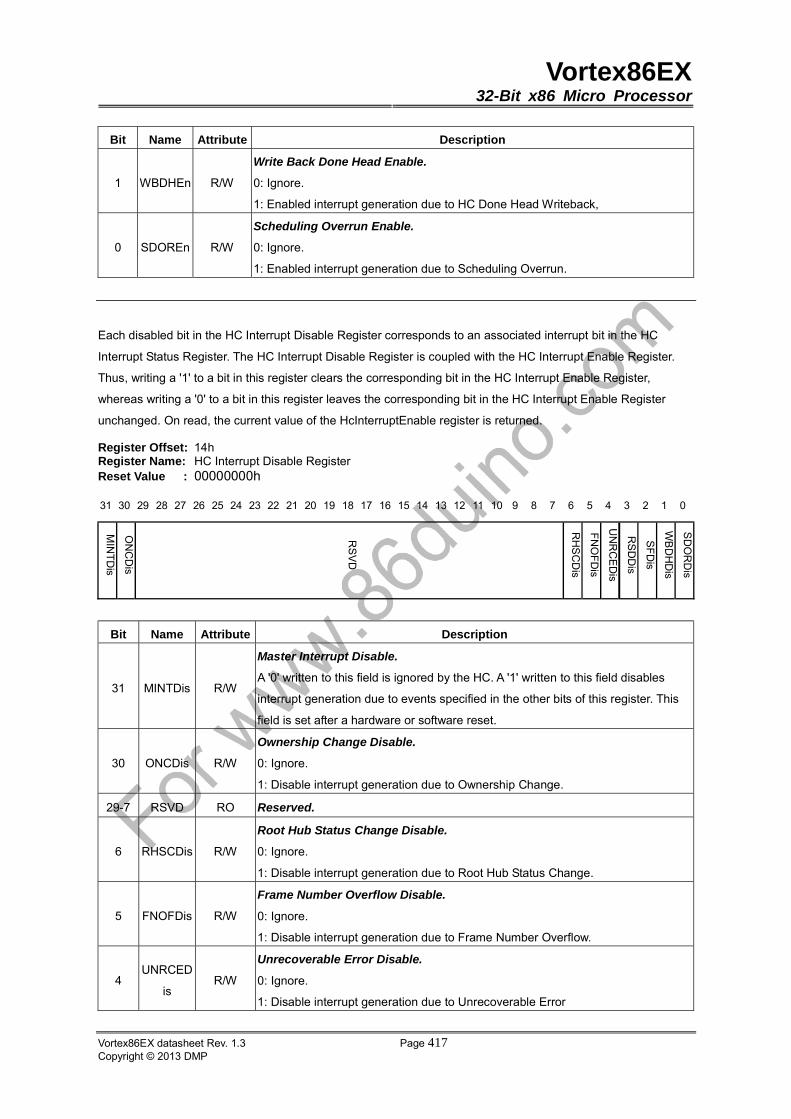
Vortex86EX32-Bit x86 Micro Processor
Vortex86EX datasheet Rev. 1.3 Page 417Copyright © 2013 DMP
Bit Name Attribute Description
1 WBDHEn R/W
Write Back Done Head Enable.
0: Ignore.
1: Enabled interrupt generation due to HC Done Head Writeback,
0 SDOREn R/W
Scheduling Overrun Enable.
0: Ignore.
1: Enabled interrupt generation due to Scheduling Overrun.
Each disabled bit in the HC Interrupt Disable Register corresponds to an associated interrupt bit in the HC
Interrupt Status Register. The HC Interrupt Disable Register is coupled with the HC Interrupt Enable Register.
Thus, writing a '1' to a bit in this register clears the corresponding bit in the HC Interrupt Enable Register,
whereas writing a '0' to a bit in this register leaves the corresponding bit in the HC Interrupt Enable Register
unchanged. On read, the current value of the HcInterruptEnable register is returned.
Register Offset: 14h Register Name: HC Interrupt Disable Register Reset Value : 00000000h
31 30 29 28 27 26 25 24 23 22 21 20 19 18 17 16 15 14 13 12 11 10 9 8 7 6 5 4 3 2 1 0
Bit Name Attribute Description
31 MINTDis R/W
Master Interrupt Disable.
A '0' written to this field is ignored by the HC. A '1' written to this field disables
interrupt generation due to events specified in the other bits of this register. This
field is set after a hardware or software reset.
30 ONCDis R/W
Ownership Change Disable.
0: Ignore.
1: Disable interrupt generation due to Ownership Change.
29-7 RSVD RO Reserved.
6 RHSCDis R/W
Root Hub Status Change Disable.
0: Ignore.
1: Disable interrupt generation due to Root Hub Status Change.
5 FNOFDis R/W
Frame Number Overflow Disable.
0: Ignore.
1: Disable interrupt generation due to Frame Number Overflow.
4 UNRCED
is R/W
Unrecoverable Error Disable.
0: Ignore.
1: Disable interrupt generation due to Unrecoverable Error
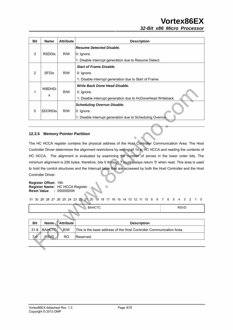
Vortex86EX32-Bit x86 Micro Processor
Vortex86EX datasheet Rev. 1.3 Page 418Copyright © 2013 DMP
Bit Name Attribute Description
3 RSDDis R/W
Resume Detected Disable.
0: Ignore.
1: Disable interrupt generation due to Resume Detect.
2 SFDis R/W
Start of Frame Disable.
0: Ignore.
1: Disable interrupt generation due to Start of Frame.
1 WBDHDi
s R/W
Write Back Done Head Disable.
0: Ignore.
1: Disable interrupt generation due to HcDoneHead Writeback.
0 SDORDis R/W
Scheduling Overrun Disable.
0: Ignore.
1: Disable interrupt generation due to Scheduling Overrun.
12.3.5 Memory Pointer Partition
The HC HCCA register contains the physical address of the Host Controller Communication Area. The Host
Controller Driver determines the alignment restrictions by writing all 1s to HC HCCA and reading the contents of
HC HCCA. The alignment is evaluated by examining the number of zeroes in the lower order bits. The
minimum alignment is 256 bytes; therefore, bits 0 through 7 must always return '0' when read. This area is used
to hold the control structures and the Interrupt table that are accessed by both the Host Controller and the Host
Controller Driver.
Register Offset: 18h Register Name: HC HCCA Register Reset Value : 00000000h
31 30 29 28 27 26 25 24 23 22 21 20 19 18 17 16 15 14 13 12 11 10 9 8 7 6 5 4 3 2 1 0
BAHCTC RSVD
Bit Name Attribute Description
31-8 BAHCTC R/W This is the base address of the Host Controller Communication Area.
7-0 RSVD RO Reserved.
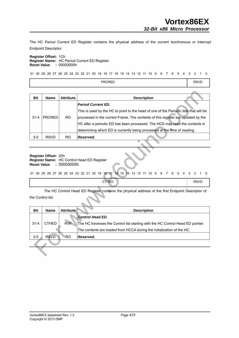
Vortex86EX32-Bit x86 Micro Processor
Vortex86EX datasheet Rev. 1.3 Page 419Copyright © 2013 DMP
The HC Period Current ED Register contains the physical address of the current Isochronous or Interrupt
Endpoint Descriptor.
Register Offset: 1Ch Register Name: HC Period Current ED Register Reset Value : 00000000h
31 30 29 28 27 26 25 24 23 22 21 20 19 18 17 16 15 14 13 12 11 10 9 8 7 6 5 4 3 2 1 0
PRCRED RSVD
Bit Name Attribute Description
31-4 PRCRED RO
Period Current ED.
This is used by the HC to point to the head of one of the Periodic lists that will be
processed in the current Frame. The contents of this register are updated by the
HC after a periodic ED has been processed. The HCD may read the contents in
determining which ED is currently being processed at the time of reading.
3-0 RSVD RO Reserved.
Register Offset: 20h Register Name: HC Control Head ED Register Reset Value : 00000000h
31 30 29 28 27 26 25 24 23 22 21 20 19 18 17 16 15 14 13 12 11 10 9 8 7 6 5 4 3 2 1 0
CTHED RSVD
The HC Control Head ED Register contains the physical address of the first Endpoint Descriptor of
the Control list.
Bit Name Attribute Description
31-4 CTHED R/W
Control Head ED.
The HC traverses the Control list starting with the HC Control Head ED pointer.
The contents are loaded from HCCA during the initialization of the HC.
3-0 RSVD RO Reserved.
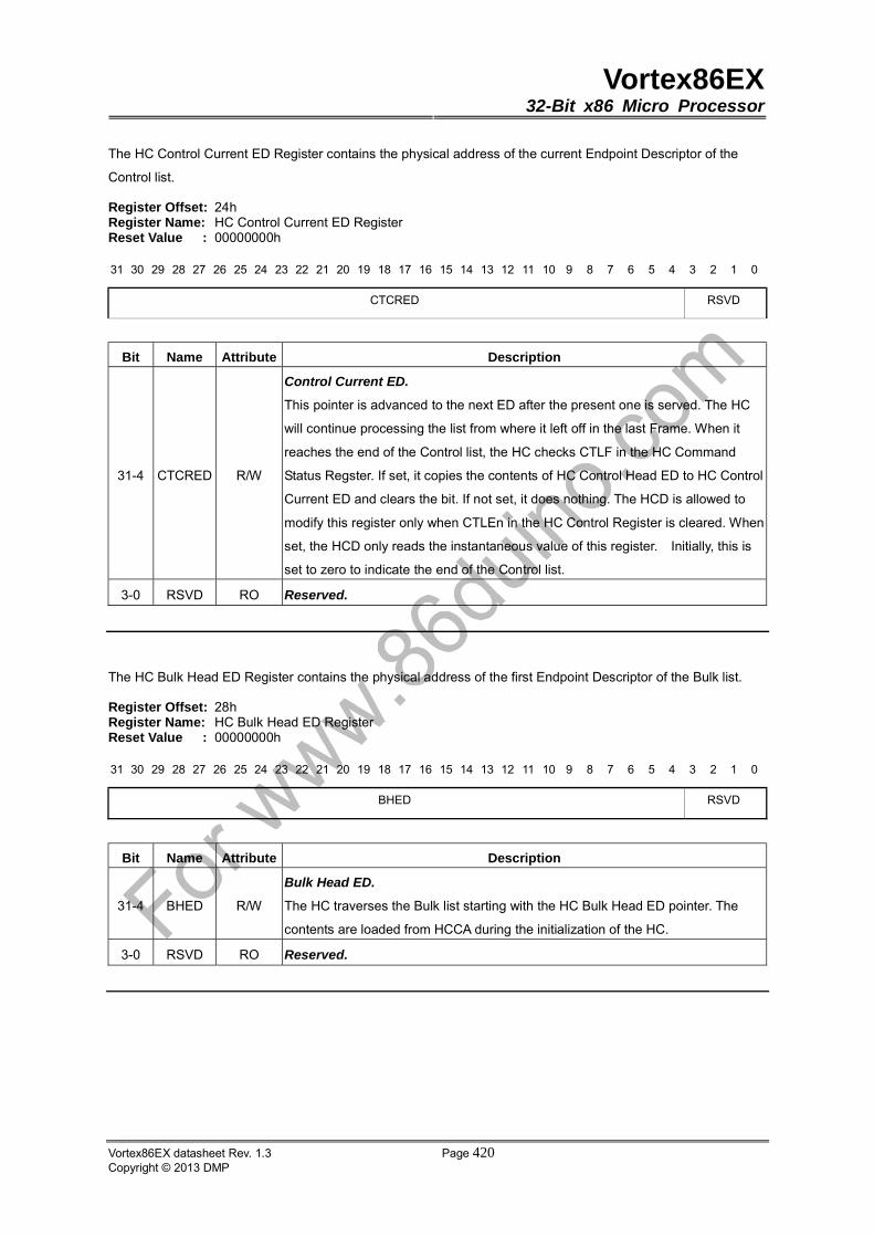
Vortex86EX32-Bit x86 Micro Processor
Vortex86EX datasheet Rev. 1.3 Page 420Copyright © 2013 DMP
The HC Control Current ED Register contains the physical address of the current Endpoint Descriptor of the
Control list.
Register Offset: 24h Register Name: HC Control Current ED Register Reset Value : 00000000h
31 30 29 28 27 26 25 24 23 22 21 20 19 18 17 16 15 14 13 12 11 10 9 8 7 6 5 4 3 2 1 0
CTCRED RSVD
Bit Name Attribute Description
31-4 CTCRED R/W
Control Current ED.
This pointer is advanced to the next ED after the present one is served. The HC
will continue processing the list from where it left off in the last Frame. When it
reaches the end of the Control list, the HC checks CTLF in the HC Command
Status Regster. If set, it copies the contents of HC Control Head ED to HC Control
Current ED and clears the bit. If not set, it does nothing. The HCD is allowed to
modify this register only when CTLEn in the HC Control Register is cleared. When
set, the HCD only reads the instantaneous value of this register. Initially, this is
set to zero to indicate the end of the Control list.
3-0 RSVD RO Reserved.
The HC Bulk Head ED Register contains the physical address of the first Endpoint Descriptor of the Bulk list.
Register Offset: 28h Register Name: HC Bulk Head ED Register Reset Value : 00000000h
31 30 29 28 27 26 25 24 23 22 21 20 19 18 17 16 15 14 13 12 11 10 9 8 7 6 5 4 3 2 1 0
BHED RSVD
Bit Name Attribute Description
31-4 BHED R/W
Bulk Head ED.
The HC traverses the Bulk list starting with the HC Bulk Head ED pointer. The
contents are loaded from HCCA during the initialization of the HC.
3-0 RSVD RO Reserved.
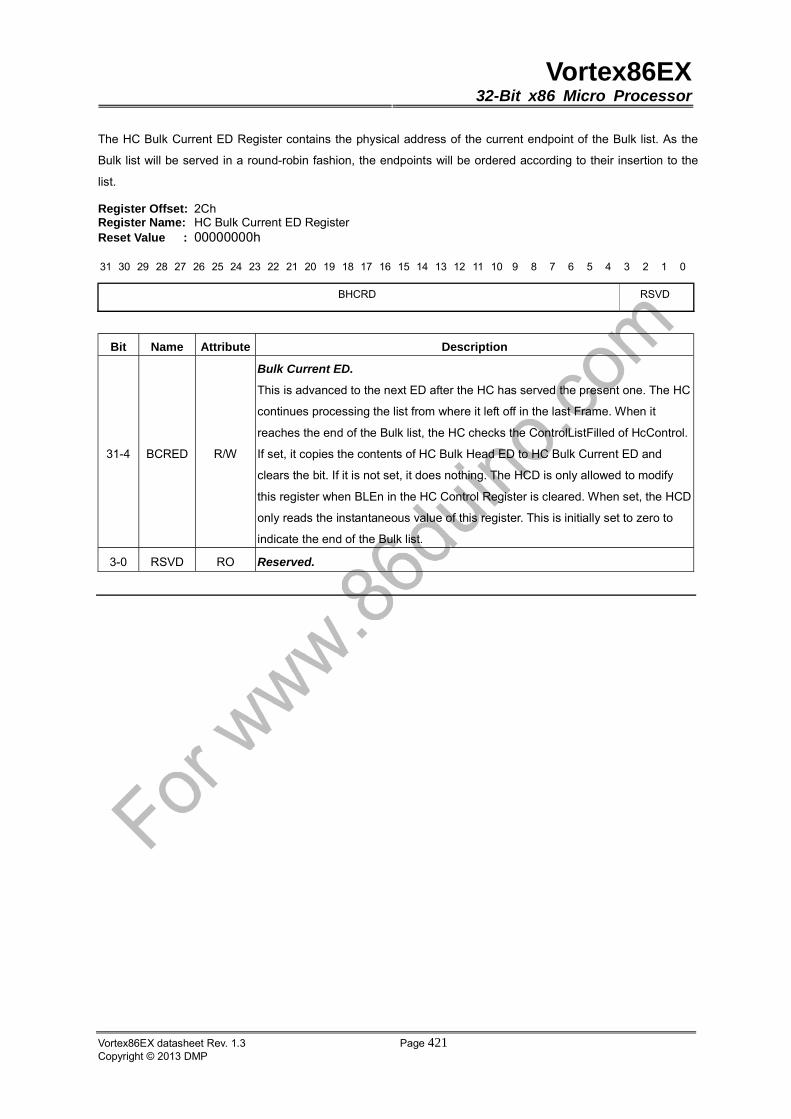
Vortex86EX32-Bit x86 Micro Processor
Vortex86EX datasheet Rev. 1.3 Page 421Copyright © 2013 DMP
The HC Bulk Current ED Register contains the physical address of the current endpoint of the Bulk list. As the
Bulk list will be served in a round-robin fashion, the endpoints will be ordered according to their insertion to the
list.
Register Offset: 2Ch Register Name: HC Bulk Current ED Register Reset Value : 00000000h
31 30 29 28 27 26 25 24 23 22 21 20 19 18 17 16 15 14 13 12 11 10 9 8 7 6 5 4 3 2 1 0
BHCRD RSVD
Bit Name Attribute Description
31-4 BCRED R/W
Bulk Current ED.
This is advanced to the next ED after the HC has served the present one. The HC
continues processing the list from where it left off in the last Frame. When it
reaches the end of the Bulk list, the HC checks the ControlListFilled of HcControl.
If set, it copies the contents of HC Bulk Head ED to HC Bulk Current ED and
clears the bit. If it is not set, it does nothing. The HCD is only allowed to modify
this register when BLEn in the HC Control Register is cleared. When set, the HCD
only reads the instantaneous value of this register. This is initially set to zero to
indicate the end of the Bulk list.
3-0 RSVD RO Reserved.
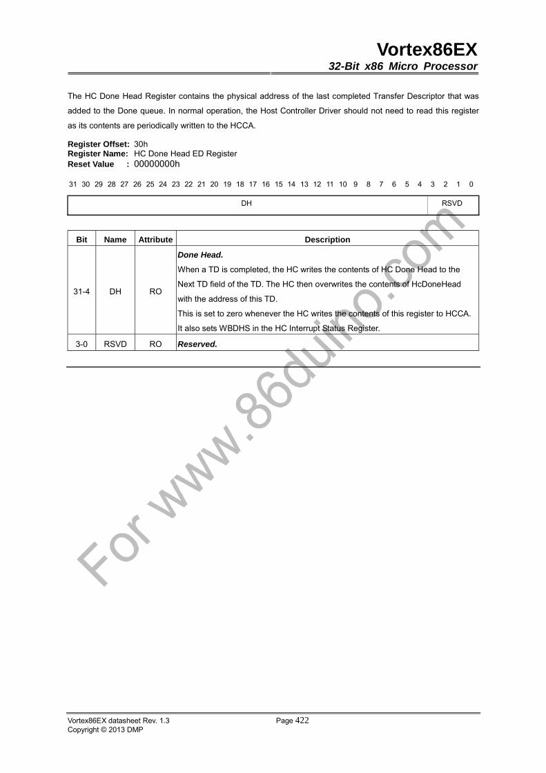
Vortex86EX32-Bit x86 Micro Processor
Vortex86EX datasheet Rev. 1.3 Page 422Copyright © 2013 DMP
The HC Done Head Register contains the physical address of the last completed Transfer Descriptor that was
added to the Done queue. In normal operation, the Host Controller Driver should not need to read this register
as its contents are periodically written to the HCCA.
Register Offset: 30h Register Name: HC Done Head ED Register Reset Value : 00000000h
31 30 29 28 27 26 25 24 23 22 21 20 19 18 17 16 15 14 13 12 11 10 9 8 7 6 5 4 3 2 1 0
DH RSVD
Bit Name Attribute Description
31-4 DH RO
Done Head.
When a TD is completed, the HC writes the contents of HC Done Head to the
Next TD field of the TD. The HC then overwrites the contents of HcDoneHead
with the address of this TD.
This is set to zero whenever the HC writes the contents of this register to HCCA.
It also sets WBDHS in the HC Interrupt Status Register.
3-0 RSVD RO Reserved.
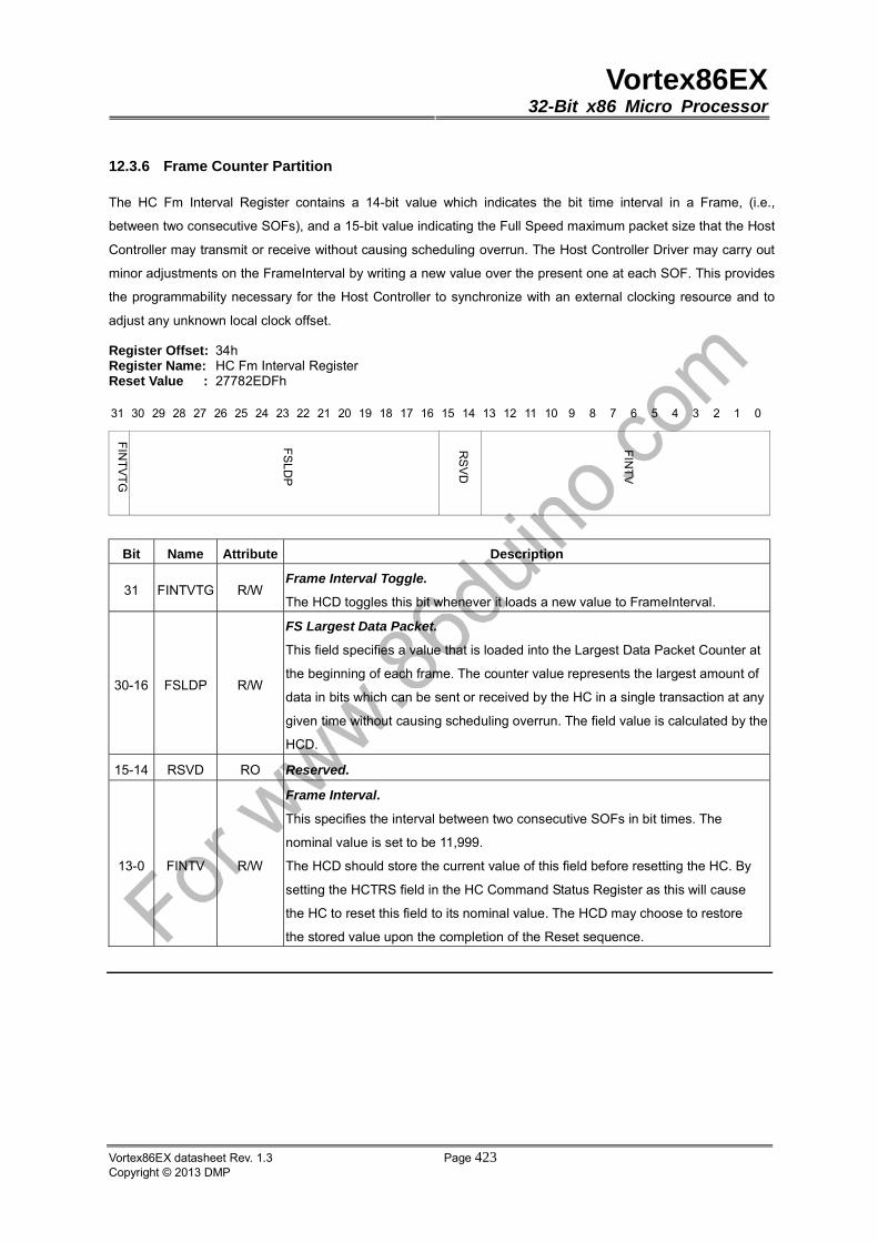
Vortex86EX32-Bit x86 Micro Processor
Vortex86EX datasheet Rev. 1.3 Page 423Copyright © 2013 DMP
12.3.6 Frame Counter Partition
The HC Fm Interval Register contains a 14-bit value which indicates the bit time interval in a Frame, (i.e.,
between two consecutive SOFs), and a 15-bit value indicating the Full Speed maximum packet size that the Host
Controller may transmit or receive without causing scheduling overrun. The Host Controller Driver may carry out
minor adjustments on the FrameInterval by writing a new value over the present one at each SOF. This provides
the programmability necessary for the Host Controller to synchronize with an external clocking resource and to
adjust any unknown local clock offset.
Register Offset: 34h Register Name: HC Fm Interval Register Reset Value : 27782EDFh
31 30 29 28 27 26 25 24 23 22 21 20 19 18 17 16 15 14 13 12 11 10 9 8 7 6 5 4 3 2 1 0
Bit Name Attribute Description
31 FINTVTG R/W Frame Interval Toggle.
The HCD toggles this bit whenever it loads a new value to FrameInterval.
30-16 FSLDP R/W
FS Largest Data Packet.
This field specifies a value that is loaded into the Largest Data Packet Counter at
the beginning of each frame. The counter value represents the largest amount of
data in bits which can be sent or received by the HC in a single transaction at any
given time without causing scheduling overrun. The field value is calculated by the
HCD.
15-14 RSVD RO Reserved.
13-0 FINTV R/W
Frame Interval.
This specifies the interval between two consecutive SOFs in bit times. The
nominal value is set to be 11,999.
The HCD should store the current value of this field before resetting the HC. By
setting the HCTRS field in the HC Command Status Register as this will cause
the HC to reset this field to its nominal value. The HCD may choose to restore
the stored value upon the completion of the Reset sequence.

Vortex86EX32-Bit x86 Micro Processor
Vortex86EX datasheet Rev. 1.3 Page 424Copyright © 2013 DMP
The HC Fm Remaining Register is a 14-bit down counter showing the bit time remaining in the current Frame.
Register Offset: 38h Register Name: HC Fm Remaining Register Reset Value : 00000000h
31 30 29 28 27 26 25 24 23 22 21 20 19 18 17 16 15 14 13 12 11 10 9 8 7 6 5 4 3 2 1 0
Bit Name Attribute Description
31 FRMTG RO
Frame Remaining Toggle.
This bit is loaded from the Frame Interval Toggle field in the HC Fm Interval
Register whenever Frame Remaining reaches 0. This bit is used by the HCD for
the synchronization between Frame Interval and Frame Remaining.
30-14 RSVD RO Reserved.
13-0 FRM RO
Frame Remaining.
This counter is decremented at each bit time. When it reaches zero, it is reset by
loading the Frame Interval value specified in the HC Fm Interval Register at the
next bit time boundary. When entering the USB Operational state, the HC
re-loads the content with the Frame Interval in the HC Fm Interval Register and
uses the updated value from the next SOF.

Vortex86EX32-Bit x86 Micro Processor
Vortex86EX datasheet Rev. 1.3 Page 425Copyright © 2013 DMP
The HC Fm Number Register is a 16-bit counter. It provides a timing reference among events occurring in the
Host Controller and the Host Controller Driver. The Host Controller Driver may use the 16-bit value specified in
this register and generate a 32-bit frame number without requiring frequent access to the register.
Register Offset: 3Ch Register Name: HC Fm Number Register Reset Value : 00000000h
31 30 29 28 27 26 25 24 23 22 21 20 19 18 17 16 15 14 13 12 11 10 9 8 7 6 5 4 3 2 1 0
RSVD FNB
Bit Name Attribute Description
31-16 RSVD RO Reserved.
15-0 FNB RO
Frame Number.
This is incremented when HcFmRemaining is re-loaded. It will be rolled over to
0h after ffffh. When the USB Operational state is entered, this will be incremented
automatically. The contents will be written to HCCA after the HC has incremented
the Frame Number at each frame boundary and sent a SOF but before the HC
reads the first ED in that Frame. After writing to HCCA, the HC will set the Start of
Frame in HC Interrupt Status.
The Hc Periodic Start Register has a 14-bit programmable value that determines the earliest time the HC should
start processing the periodic list.
Register Offset: 40h Register Name: HC Periodic Start Register Reset Value : 00003E67h
31 30 29 28 27 26 25 24 23 22 21 20 19 18 17 16 15 14 13 12 11 10 9 8 7 6 5 4 3 2 1 0
RSVD PRS
Bit Name Attribute Description
31-14 RSVD RO Reserved.
13-0 PRS R/W
Periodic Start.
After a hardware reset, this field is cleared. This is then set by the HCD during
the HC initialization. The value is calculated roughly as 10% off from the HC Fm
Interval Register. A typical value will be 3E67h. When HC Fm Remaining reaches
the value specified, processing of the periodic lists will have priority over
Control/Bulk processing. The HC will therefore start processing the Interrupt list
after completing the current Control or Bulk transaction that is in progress.

Vortex86EX32-Bit x86 Micro Processor
Vortex86EX datasheet Rev. 1.3 Page 426Copyright © 2013 DMP
The HC LS Threshold register contains an 11-bit value used by the Host Controller to determine whether it is
necessary to commit to the transfer of a maximum of 8-byte LS packets before EOF. Neither the Host Controller
nor the Host Controller Driver is allowed to change this value.
Register Offset: 44h Register Name: HC LS Threshold Register Reset Value : 00000628h
31 30 29 28 27 26 25 24 23 22 21 20 19 18 17 16 15 14 13 12 11 10 9 8 7 6 5 4 3 2 1 0
RSVD LSTSH
Bit Name Attribute Description
31-12 RSVD RO Reserved.
11-0 LSTSH R/W
LS Threshold.
This field contains a value that is compared to the Frame Remaining field prior to
initiating a Low Speed transaction. The transaction is started only if Frame
Remaining � this field. The value is calculated by the HCD with the consideration
of transmission and set-up overhead.
Vortex86EX32-Bit x86 Micro Processor
Vortex86EX datasheet Rev. 1.3 Page 427Copyright © 2013 DMP
12.3.7 Root Hub Partition
All registers included in this partition are dedicated to the USB Root Hub which is an integral part of the Host
Controller though still a functionally separate entity. The HCD emulates USBD accesses to the Root Hub via a
register interface. The HCD maintains many USB-defined hub features that are not required to be supported in
hardware. For example, the Hub's Device, Configuration, Interface, and Endpoint Descriptors are maintained only
in the HCD as well as some static fields of the Class Descriptor. The HCD also maintains and decodes the Root
Hub's device address as well as other trivial operations that are better suited to software than hardware.
The Root Hub register interface is otherwise developed to maintain similarity of bit organization and operation to
typical hubs that are found in the system. Below are four register definitions: HC Rh Descriptor A, HC Rh
Descriptor B, HC Rh Status, and HC Rh Port Status [5:1]. Each register is read and written as a Dword. These
registers are only written during initialization to correspond with the system implementation. The HC Rh
Descriptor A and HC Rh Descriptor B registers should be implemented such that they are writable regardless of
the HC USB state. HC Rh Status and HC Rh Port Status must be writable during the USB Operational state.

Vortex86EX32-Bit x86 Micro Processor
Vortex86EX datasheet Rev. 1.3 Page 428Copyright © 2013 DMP
The HC Rh Descriptor A Register is the first register of two describing characteristics of the Root Hub. Reset
values are implementation-specific. All other fields are located in the HC Rh Descriptor A and HC Rh Descriptor
B registers.
Register Offset: 48h Register Name: HC Rh Discriptor A Register Reset Value : 0F000904h
31 30 29 28 27 26 25 24 23 22 21 20 19 18 17 16 15 14 13 12 11 10 9 8 7 6 5 4 3 2 1 0
Bit Name Attribute Description
31-24 POPGT R/W
Power On to Power Good Time.
This byte specifies the duration the HCD has to wait before a powered-on port of
the Root Hub is accessed. It is implementation-specific. The unit of time is 2 ms.
The duration is calculated as POTPGT * 2 ms.
23-13 RSVD RO Reserved.
12 NOCRPT R/W
No Over Current Protection.
This bit describes how the over-current status for the Root Hub ports is reported.
When this bit is cleared, the Over Current Protection Mode field specifies global
or per-port reporting.
0: Over-current status is reported collectively for all downstream ports.
1: No over-current protection supported.
11 OCRPTM R/W
Over Current Protection Mode.
This bit describes how the over-current status for the Root Hub ports is reported.
At reset, this field should reflect the same mode as Power Switching Mode. This
field is valid only if the No Over Current Protection field is cleared.
0: Over-current status is reported collectively for all downstream ports.
1: Over-current status is reported on a per-port basis.
10 DVT RO
Device Type.
This bit specifies that the Root Hub is not a compound device. The Root Hub is
not permitted to be a compound device. This field should always read/write 0.
9 NPSW R/W
No Power Switching.
These bits are used to specify whether power switching is supported or ports are
always powered. USB HC supports global power switching mode. When this bit
is cleared, the Power Switching Mode specifies global or per-port switching.
0: Ports are power switched.
1: Ports are always powered on when the HC is powered on.
8 PSWM R/W Power Switching Mode.
This bit is used to specify how the power switching of the Root Hub ports is
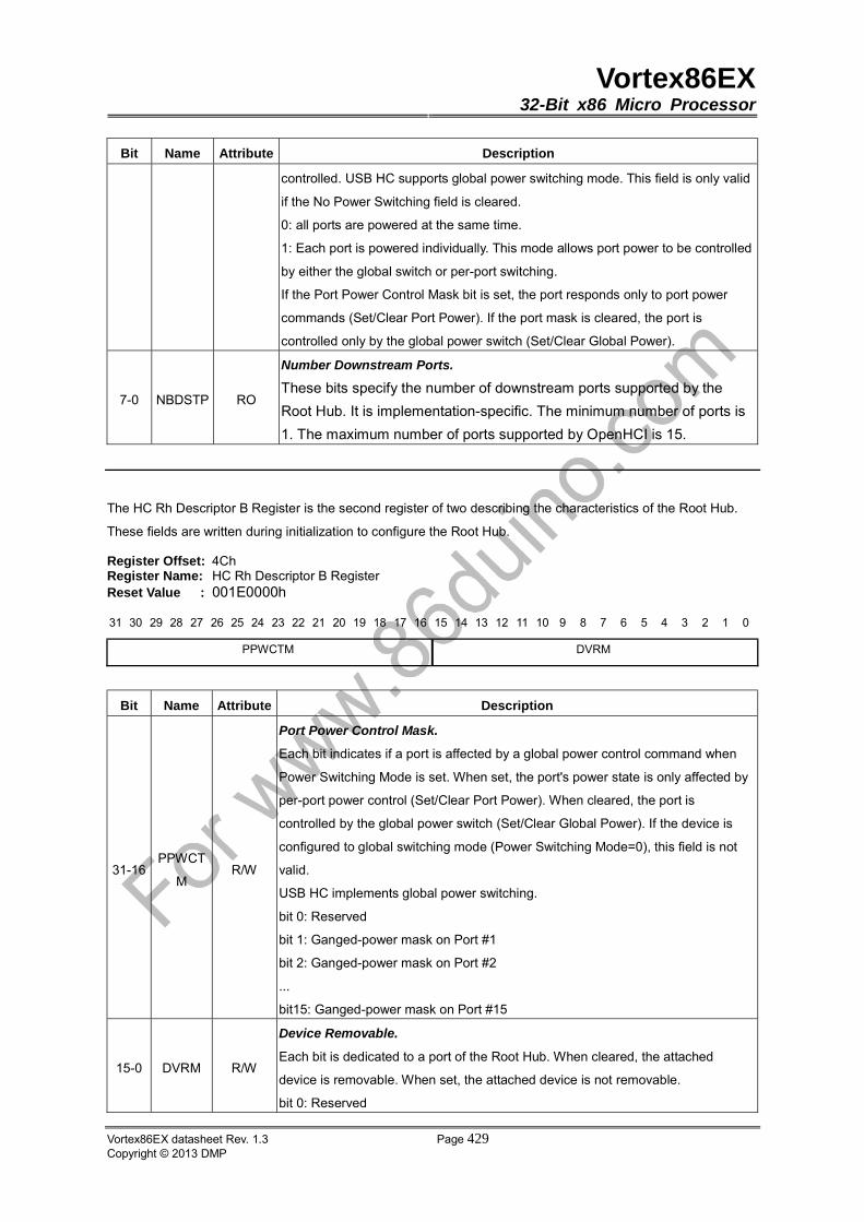
Vortex86EX32-Bit x86 Micro Processor
Vortex86EX datasheet Rev. 1.3 Page 429Copyright © 2013 DMP
Bit Name Attribute Description
controlled. USB HC supports global power switching mode. This field is only valid
if the No Power Switching field is cleared.
0: all ports are powered at the same time.
1: Each port is powered individually. This mode allows port power to be controlled
by either the global switch or per-port switching.
If the Port Power Control Mask bit is set, the port responds only to port power
commands (Set/Clear Port Power). If the port mask is cleared, the port is
controlled only by the global power switch (Set/Clear Global Power).
7-0 NBDSTP RO
Number Downstream Ports.
These bits specify the number of downstream ports supported by the
Root Hub. It is implementation-specific. The minimum number of ports is
1. The maximum number of ports supported by OpenHCI is 15.
The HC Rh Descriptor B Register is the second register of two describing the characteristics of the Root Hub.
These fields are written during initialization to configure the Root Hub.
Register Offset: 4Ch Register Name: HC Rh Descriptor B Register Reset Value : 001E0000h
31 30 29 28 27 26 25 24 23 22 21 20 19 18 17 16 15 14 13 12 11 10 9 8 7 6 5 4 3 2 1 0
PPWCTM DVRM
Bit Name Attribute Description
31-16PPWCT
M R/W
Port Power Control Mask.
Each bit indicates if a port is affected by a global power control command when
Power Switching Mode is set. When set, the port's power state is only affected by
per-port power control (Set/Clear Port Power). When cleared, the port is
controlled by the global power switch (Set/Clear Global Power). If the device is
configured to global switching mode (Power Switching Mode=0), this field is not
valid.
USB HC implements global power switching.
bit 0: Reserved
bit 1: Ganged-power mask on Port #1
bit 2: Ganged-power mask on Port #2
...
bit15: Ganged-power mask on Port #15
15-0 DVRM R/W
Device Removable.
Each bit is dedicated to a port of the Root Hub. When cleared, the attached
device is removable. When set, the attached device is not removable.
bit 0: Reserved

Vortex86EX32-Bit x86 Micro Processor
Vortex86EX datasheet Rev. 1.3 Page 430Copyright © 2013 DMP
Bit Name Attribute Description
bit 1: Device attached to Port #1
bit 2: Device attached to Port #2
...
bit15: Device attached to Port #15
The HC Rh Status Register is divided into two parts. The lower word of a Dword represents the Hub Status field
and the upper word represents the Hub Status Change field. Reserved bits should always be written '0'.
Register Offset: 50h Register Name: HC Rh Status Register Reset Value : 00000000h
31 30 29 28 27 26 25 24 23 22 21 20 19 18 17 16 15 14 13 12 11 10 9 8 7 6 5 4 3 2 1 0
Bit Name Attribute Description
31 CRMWEn WO Clear Remote Wakeup Enable (Write).
Writing a '1' clears Device Remove Wakeup Enable. Writing a '0' has no effect.
31-18 RSVD RO Reserved.
17 OCRIDC R/W
Over Current Indicator Change.
This bit is set by hardware when a change has occurred to the OCI field of this
register. The HCD clears this bit by writing a '1'.Writing a ‘0’ has no effect.
16 LPSC R/W
Local Power Status Change (Read).
The Root Hub does not support the local power status feature; thus, this bit is
always read as '0'.
Set Global Power (Write).
In global power mode (Power Switching Mode=0), this bit is written to '1' to turn
on power to all ports (clear Port Power Status). In per-port power mode, it sets
Port Power Status only on ports whose Port Power Control Mask bit is not set.
Writing a ‘0’ has no effect.
15 DRWE R/W
Device Remote Wakeup Enable (Read).
This bit enables a Connect Status Change bit as a resume event, causing an
USB Suspend to USB Resume state transition and setting Resume Detected
interrupt.
0: Connect Status Change is not a remote wakeup event.
1: Connect Status Change is a remote wakeup event.
Set Remote Wakeup Enable (Write).
Writing a '1' sets Device Remove Wakeup Enable. Writing a '0' has no effect.

Vortex86EX32-Bit x86 Micro Processor
Vortex86EX datasheet Rev. 1.3 Page 431Copyright © 2013 DMP
Bit Name Attribute Description
14-2 RSVD RO Reserved.
1 OCRID RO
Over Current Indicator.
This bit reports over-current conditions when the global reporting is implemented.
When set, an over-current condition exists. When cleared, all power operations
are normal. If per-port over-current protection is implemented, this bit is always
‘0’
0 LPS R/W
Local Power Status (Read).
The Root Hub does not support the local power status feature; thus, this bit is
always read as '0'.
Clear Global Power (Write).
In global power mode (Power Switching Mode=0), This bit is written to '1' to turn
off power to all ports (clear Port Power Status). In per-port power mode, it clears
Port Power Status only on ports whose Port Power Control Mask bit is not set.
Writing a ‘0’ has no effect.
The HC Rh Port Status [3:0] registers are used to control and report port events on a per-port basis. Two HC
Rh Port Status registers are implemented in this HC, respectively. The lower word is used to reflect the port
status, whereas the upper word reflects the status change bits. Some status bits are implemented with special
write behaviour (see below). If a transaction (token through handshake) is in progress when a write to change
port status occurs, the resulting port status change must be postponed until the transaction is completed.
Reserved bits should always be written as '0'. While the NDP of register 48h is 01h, the register 58 and
register 5C will be read as 00000000h. While the NDP of register 48h is 02h, only register 5C is read as
00000000h.
Register Offset: 54h/58h Register Name: HC Rh Port Status [1:0] Register Reset Value : 00000000h
31 30 29 28 27 26 25 24 23 22 21 20 19 18 17 16 15 14 13 12 11 10 9 8 7 6 5 4 3 2 1 0
Bit Name Attribute Description
31-21 RSVD RO Reserved.
20 PRSC R/W
Port Reset Status Change.
This bit is set at the end of the 10-ms port reset signal.
The HCD writes a '1' to clear this bit. Writing a '0' has no effect.
0: port reset is not complete
1: port reset is complete

Vortex86EX32-Bit x86 Micro Processor
Vortex86EX datasheet Rev. 1.3 Page 432Copyright © 2013 DMP
Bit Name Attribute Description
19 POCRID
C R/W
Port Over Current Indicator Change.
This bit is valid only if over-current conditions are reported on a per-port basis.
This bit is set when Root Hub changes the Port Over Current Indicator bit. The
HCD writes a '1' to clear this bit. Writing a '0' has no effect.
0: no change in Port Over Current Indicator
1: Port Over Current Indicator has changed
18 PSPSC R/W
Port Suspend Status Change.
This bit is set when the full resume sequence has been completed. This
sequence includes the 20-s resume pulse, LS EOP, and 3-ms resynchronization
delay. The HCD writes a '1' to clear this bit. Writing a '0' has no effect. This bit is
also cleared when Reset Status Change is set.
0: resume is not completed
1: resume completed
17 PEnSC R/W
Port Enable Status Change.
This bit is set when hardware events cause the Port Enable Status bit to be
cleared. Changes from the HCD writes do not set this bit. The HCD writes a '1' to
clear this bit. Writing a '0' has no effect.
0: no change in Port Enable Status
1: change in Port Enable Status
16 CNSC R/W
Connect Status Change.
This bit is set whenever a connect or disconnect event occurs. The HCD writes a
'1' to clear this bit. Writing a '0' has no effect. If Current Connect Status is cleared
when a Set Port Reset, Set Port Enable, or Set Port Suspend write occurs, this
bit is set to force the driver to re-evaluate the connection status since these
writes should not occur if the port is disconnected.
0: no change in Current Connect Status.
1: change in Current Connect Status.
Note: If the Device Removable [NDP] bit is set, this bit is set only after a Root
Hub reset to inform the system that the device is attached.
15-10 RSVD RO Reserved.
9 LSDVA R/W
Low Speed Device Attached (Read).
This bit indicates the speed of the device attached to this port. When set, a
Low-Speed device is attached to this port. When cleared, a Full Speed device is
attached to this port. This field is valid only when the Current Connect Status is
set.
0: full-speed device attached
1: low-speed device attached
8 PPS R/W
Port Power Status (Read).
This bit reflects the port’s power status, regardless of the type of power switching
implemented. This bit is cleared if an over-current condition is detected. The HCD
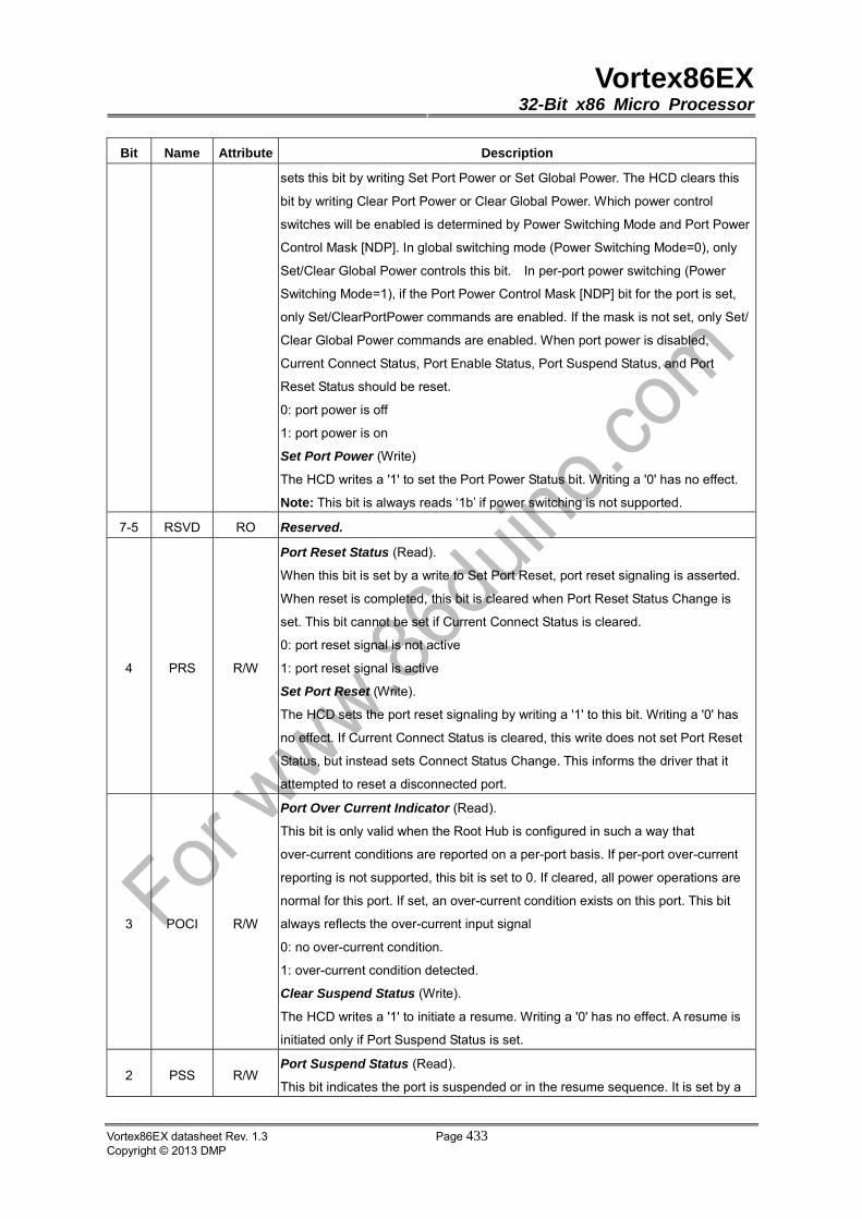
Vortex86EX32-Bit x86 Micro Processor
Vortex86EX datasheet Rev. 1.3 Page 433Copyright © 2013 DMP
Bit Name Attribute Description
sets this bit by writing Set Port Power or Set Global Power. The HCD clears this
bit by writing Clear Port Power or Clear Global Power. Which power control
switches will be enabled is determined by Power Switching Mode and Port Power
Control Mask [NDP]. In global switching mode (Power Switching Mode=0), only
Set/Clear Global Power controls this bit. In per-port power switching (Power
Switching Mode=1), if the Port Power Control Mask [NDP] bit for the port is set,
only Set/ClearPortPower commands are enabled. If the mask is not set, only Set/
Clear Global Power commands are enabled. When port power is disabled,
Current Connect Status, Port Enable Status, Port Suspend Status, and Port
Reset Status should be reset.
0: port power is off
1: port power is on
Set Port Power (Write)
The HCD writes a '1' to set the Port Power Status bit. Writing a '0' has no effect.
Note: This bit is always reads ‘1b’ if power switching is not supported.
7-5 RSVD RO Reserved.
4 PRS R/W
Port Reset Status (Read).
When this bit is set by a write to Set Port Reset, port reset signaling is asserted.
When reset is completed, this bit is cleared when Port Reset Status Change is
set. This bit cannot be set if Current Connect Status is cleared.
0: port reset signal is not active
1: port reset signal is active
Set Port Reset (Write).
The HCD sets the port reset signaling by writing a '1' to this bit. Writing a '0' has
no effect. If Current Connect Status is cleared, this write does not set Port Reset
Status, but instead sets Connect Status Change. This informs the driver that it
attempted to reset a disconnected port.
3 POCI R/W
Port Over Current Indicator (Read).
This bit is only valid when the Root Hub is configured in such a way that
over-current conditions are reported on a per-port basis. If per-port over-current
reporting is not supported, this bit is set to 0. If cleared, all power operations are
normal for this port. If set, an over-current condition exists on this port. This bit
always reflects the over-current input signal
0: no over-current condition.
1: over-current condition detected.
Clear Suspend Status (Write).
The HCD writes a '1' to initiate a resume. Writing a '0' has no effect. A resume is
initiated only if Port Suspend Status is set.
2 PSS R/W Port Suspend Status (Read).
This bit indicates the port is suspended or in the resume sequence. It is set by a

Vortex86EX32-Bit x86 Micro Processor
Vortex86EX datasheet Rev. 1.3 Page 434Copyright © 2013 DMP
Bit Name Attribute Description
Set Suspend State write and cleared when Port Suspend Status Change is set at
the end of the resume interval. This bit cannot be set if Current Connect Status is
cleared. This bit is also cleared when Port Reset Status Change is set at the end
of the port reset or when the HC is placed in the USB Resume state. If an
upstream resume is in progress, it should propagate to the HC.
0: port is not suspended.
1: port is suspended.
Set Port Suspend (Write).
The HCD sets the Port Suspend Status bit by writing a '1' to this bit. Writing a '0'
has no effect. If Current Connect Status is cleared, this write does not set Port
Suspend Status; instead it sets Connect Status Change. This informs the driver
that it attempts to suspend a disconnected port.
1 PES R/W
Port Enable Status (Read).
This bit indicates whether the port is enabled or disabled. The Root Hub may
clear this bit when an over-current condition, disconnect event, switched-off
power, or operational bus error such as babble is detected. This change also
causes Port Enabled Status Change to be set. The HCD sets this bit by writing
Set Port Enable and clears it by writing Clear Port Enable. This bit cannot be set
when Current Connect Status is cleared. This bit is also set, if not already, at the
completion of a port reset when Reset Status Change is set or a port suspend
when Suspend Status Change is set.
0: port is disabled.
1: port is enabled.
Set Port Enable (Write).
The HCD sets Port Enable Status by writing a '1'. Writing a '0' has no effect. If
Current Connect Status is cleared, this write does not set Port Enable Status, but
instead sets Connect Status Change. This informs the driver that it attempts to
enable a disconnected port.
0 CCS R/W
Current Connect Status (Read).
This bit reflects the current state of the downstream port.
0: no device connected.
1: device connected.
Clear Port Enable (Write).
The HCD writes a '1' to this bit to clear the Port Enable Status bit. Writing a '0'
has no effect. Current Connect Status is not affected by any write.
Note: This bit is always read as ‘1b’ when the attached device is non-removable
(Device Removeable [NDP]).
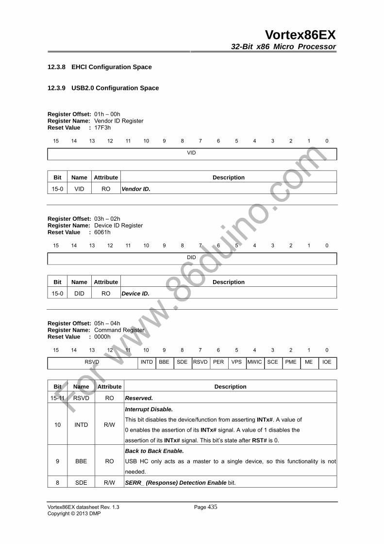
Vortex86EX32-Bit x86 Micro Processor
Vortex86EX datasheet Rev. 1.3 Page 435Copyright © 2013 DMP
12.3.8 EHCI Configuration Space
12.3.9 USB2.0 Configuration Space
Register Offset: 01h – 00h Register Name: Vendor ID Register Reset Value : 17F3h
15 14 13 12 11 10 9 8 7 6 5 4 3 2 1 0
VID
Bit Name Attribute Description
15-0 VID RO Vendor ID.
Register Offset: 03h – 02h Register Name: Device ID Register Reset Value : 6061h
15 14 13 12 11 10 9 8 7 6 5 4 3 2 1 0
DID
Bit Name Attribute Description
15-0 DID RO Device ID.
Register Offset: 05h – 04h Register Name: Command Register Reset Value : 0000h
15 14 13 12 11 10 9 8 7 6 5 4 3 2 1 0
RSVD INTD BBE SDE RSVD PER VPS MWIC SCE PME ME IOE
Bit Name Attribute Description
15-11 RSVD RO Reserved.
10 INTD R/W
Interrupt Disable.
This bit disables the device/function from asserting INTx#. A value of
0 enables the assertion of its INTx# signal. A value of 1 disables the
assertion of its INTx# signal. This bit’s state after RST# is 0.
9 BBE RO
Back to Back Enable.
USB HC only acts as a master to a single device, so this functionality is not
needed.
8 SDE R/W SERR_ (Response) Detection Enable bit.
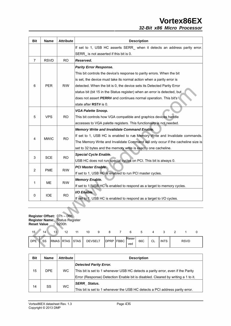
Vortex86EX32-Bit x86 Micro Processor
Vortex86EX datasheet Rev. 1.3 Page 436Copyright © 2013 DMP
Bit Name Attribute Description
If set to 1, USB HC asserts SERR_ when it detects an address parity error.
SERR_ is not asserted if this bit is 0.
7 RSVD RO Reserved.
6 PER R/W
Parity Error Response.
This bit controls the device's response to parity errors. When the bit
is set, the device must take its normal action when a parity error is
detected. When the bit is 0, the device sets its Detected Parity Error
status bit (bit 15 in the Status register) when an error is detected, but
does not assert PERR# and continues normal operation. This bit's
state after RST# is 0.
5 VPS RO
VGA Palette Snoop.
This bit controls how VGA compatible and graphics devices handle
accesses to VGA palette registers. This functionality is not needed.
4 MWIC RO
Memory Write and Invalidate Command Enable.
If set to 1, USB HC is enabled to run Memory Write and Invalidate commands.
The Memory Write and Invalidate Command will only occur if the cacheline size is
set to 32 bytes and the memory write is exactly one cacheline.
3 SCE RO Special Cycle Enable.
USB HC does not run special cycles on PCI. This bit is always 0.
2 PME R/W PCI Master Enable.
If set to 1, USB HC is enabled to run PCI master cycles.
1 ME R/W Memory Enable.
If set to 1, USB HC is enabled to respond as a target to memory cycles.
0 IOE RO I/O Enable.
If set to 1, USB HC is enabled to respond as a target to I/O cycles.
Register Offset: 07h – 06h Register Name: Status Register Reset Value : 0200h
15 14 13 12 11 10 9 8 7 6 5 4 3 2 1 0
DPE SS RMAS RTAS STAS DEVSELT DPRP FBBCReser
ved66C CL INTS RSVD
Bit Name Attribute Description
15 DPE WC
Detected Parity Error.
This bit is set to 1 whenever USB HC detects a parity error, even if the Parity
Error (Response) Detection Enable bit is disabled. Cleared by writing a 1 to it.
14 SS WC SERR_ Status.
This bit is set to 1 whenever the USB HC detects a PCI address parity error.
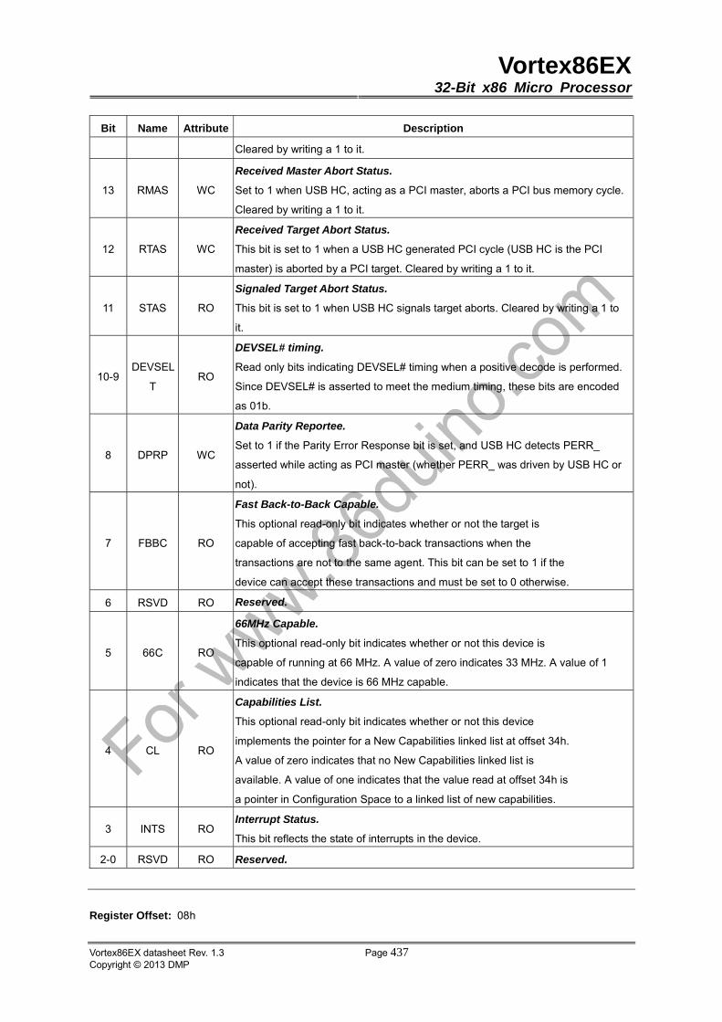
Vortex86EX32-Bit x86 Micro Processor
Vortex86EX datasheet Rev. 1.3 Page 437Copyright © 2013 DMP
Bit Name Attribute Description
Cleared by writing a 1 to it.
13 RMAS WC
Received Master Abort Status.
Set to 1 when USB HC, acting as a PCI master, aborts a PCI bus memory cycle.
Cleared by writing a 1 to it.
12 RTAS WC
Received Target Abort Status.
This bit is set to 1 when a USB HC generated PCI cycle (USB HC is the PCI
master) is aborted by a PCI target. Cleared by writing a 1 to it.
11 STAS RO
Signaled Target Abort Status.
This bit is set to 1 when USB HC signals target aborts. Cleared by writing a 1 to
it.
10-9DEVSEL
T RO
DEVSEL# timing.
Read only bits indicating DEVSEL# timing when a positive decode is performed.
Since DEVSEL# is asserted to meet the medium timing, these bits are encoded
as 01b.
8 DPRP WC
Data Parity Reportee.
Set to 1 if the Parity Error Response bit is set, and USB HC detects PERR_
asserted while acting as PCI master (whether PERR_ was driven by USB HC or
not).
7 FBBC RO
Fast Back-to-Back Capable.
This optional read-only bit indicates whether or not the target is
capable of accepting fast back-to-back transactions when the
transactions are not to the same agent. This bit can be set to 1 if the
device can accept these transactions and must be set to 0 otherwise.
6 RSVD RO Reserved.
5 66C RO
66MHz Capable.
This optional read-only bit indicates whether or not this device is
capable of running at 66 MHz. A value of zero indicates 33 MHz. A value of 1
indicates that the device is 66 MHz capable.
4 CL RO
Capabilities List.
This optional read-only bit indicates whether or not this device
implements the pointer for a New Capabilities linked list at offset 34h.
A value of zero indicates that no New Capabilities linked list is
available. A value of one indicates that the value read at offset 34h is
a pointer in Configuration Space to a linked list of new capabilities.
3 INTS RO Interrupt Status.
This bit reflects the state of interrupts in the device.
2-0 RSVD RO Reserved.
Register Offset: 08h

Vortex86EX32-Bit x86 Micro Processor
Vortex86EX datasheet Rev. 1.3 Page 438Copyright © 2013 DMP
Register Name: Revision ID Register Reset Value : 07h
7 6 5 4 3 2 1 0
FTRVL
Bit Name Attribute Description
7-0 FTRVL RO Functional Revision Level.
Register Offset: 0Bh – 09h Register Name: Class Code Register Reset Value : 0C0320h
23 22 21 20 19 18 17 16 15 14 13 12 11 10 9 8 7 6 5 4 3 2 1 0
BCLS SUBCLS PRGINTF
Bit Name Attribute Description
23-16 BCLS RO Base Class.
The Base Class is 0Ch (Serial Bus Controller).
15-8 SUBCLS RO Sub Class.
The Sub Class is 03h (Universal Serial Bus).
7-0 PRGINTF RO Programming Interface.
The Programming Interface is 20h (USB2.0).
Register Offset: 0Ch Register Name: Cache Line Size Register Reset Value : 04h
7 6 5 4 3 2 1 0
CCHLSZ
Bit Name Attribute Description
7-0 CCHLSZ R/W
Cache Line Size
This register identifies the system cache line size in units of 32-bit words. USB HC
will only store the value of 04h and 08h in this register.
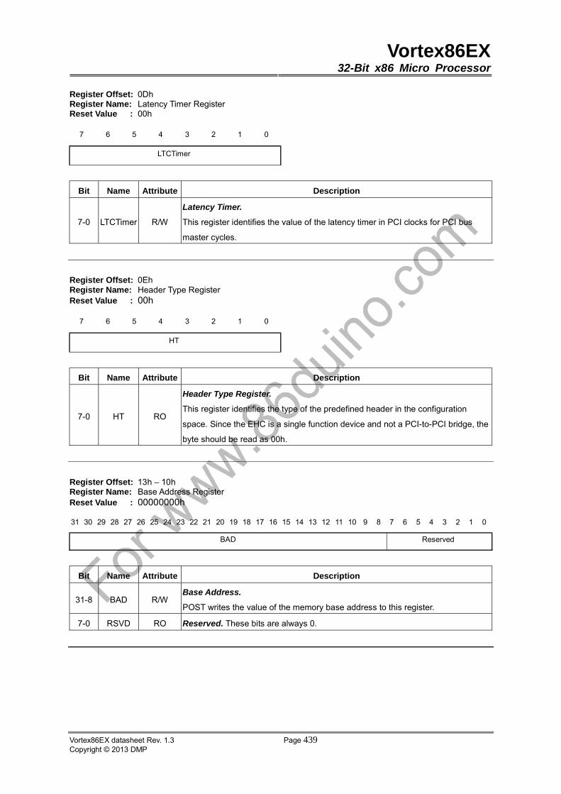
Vortex86EX32-Bit x86 Micro Processor
Vortex86EX datasheet Rev. 1.3 Page 439Copyright © 2013 DMP
Register Offset: 0Dh Register Name: Latency Timer Register Reset Value : 00h
7 6 5 4 3 2 1 0
LTCTimer
Bit Name Attribute Description
7-0 LTCTimer R/W
Latency Timer.
This register identifies the value of the latency timer in PCI clocks for PCI bus
master cycles.
Register Offset: 0Eh Register Name: Header Type Register Reset Value : 00h
7 6 5 4 3 2 1 0
HT
Bit Name Attribute Description
7-0 HT RO
Header Type Register.
This register identifies the type of the predefined header in the configuration
space. Since the EHC is a single function device and not a PCI-to-PCI bridge, the
byte should be read as 00h.
Register Offset: 13h – 10h Register Name: Base Address Register Reset Value : 00000000h
31 30 29 28 27 26 25 24 23 22 21 20 19 18 17 16 15 14 13 12 11 10 9 8 7 6 5 4 3 2 1 0
BAD Reserved
Bit Name Attribute Description
31-8 BAD R/W Base Address.
POST writes the value of the memory base address to this register.
7-0 RSVD RO Reserved. These bits are always 0.
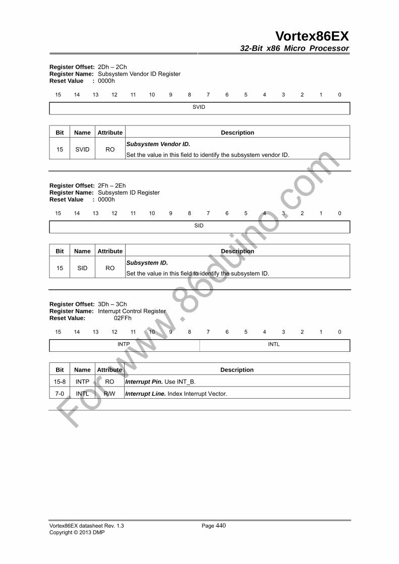
Vortex86EX32-Bit x86 Micro Processor
Vortex86EX datasheet Rev. 1.3 Page 440Copyright © 2013 DMP
Register Offset: 2Dh – 2Ch Register Name: Subsystem Vendor ID Register Reset Value : 0000h
15 14 13 12 11 10 9 8 7 6 5 4 3 2 1 0
SVID
Bit Name Attribute Description
15 SVID RO Subsystem Vendor ID.
Set the value in this field to identify the subsystem vendor ID.
Register Offset: 2Fh – 2Eh Register Name: Subsystem ID Register Reset Value : 0000h
15 14 13 12 11 10 9 8 7 6 5 4 3 2 1 0
SID
Bit Name Attribute Description
15 SID RO Subsystem ID.
Set the value in this field to identify the subsystem ID.
Register Offset: 3Dh – 3Ch Register Name: Interrupt Control Register Reset Value: 02FFh
15 14 13 12 11 10 9 8 7 6 5 4 3 2 1 0
INTP INTL
Bit Name Attribute Description
15-8 INTP RO Interrupt Pin. Use INT_B.
7-0 INTL R/W Interrupt Line. Index Interrupt Vector.

Vortex86EX32-Bit x86 Micro Processor
Vortex86EX datasheet Rev. 1.3 Page 441Copyright © 2013 DMP
Register Offset: 3Eh Register Name: Minimun Grant Register Reset Value : 00h
7 6 5 4 3 2 1 0
MINGNT
Bit Name Attribute Description
7-0 MINGNT RO
Minimum Grant.
This register specifies the desired settings for how long of a burst EHC needs
assuming a clock rate of 33 MHz. The value specifies a period of time in units of
1/4 microsecond.
Register Offset: 3Fh Register Name: Max Latency Register Reset Value : 00h
7 6 5 4 3 2 1 0
MAXLAT
Bit Name Attribute Description
7-0 MAXLAT RO
Maximum Latency.
This register specifies the desired setting for how often the EHC needs access to
the PCI bus assuming a clock rate of 33 MHz. The value specifies a period of time
in units of 1/4 microsecond.
Register Offset: 43h – 40h
Register Name: Reserved
Register Offset: 47h – 44h
Register Name: Reserved
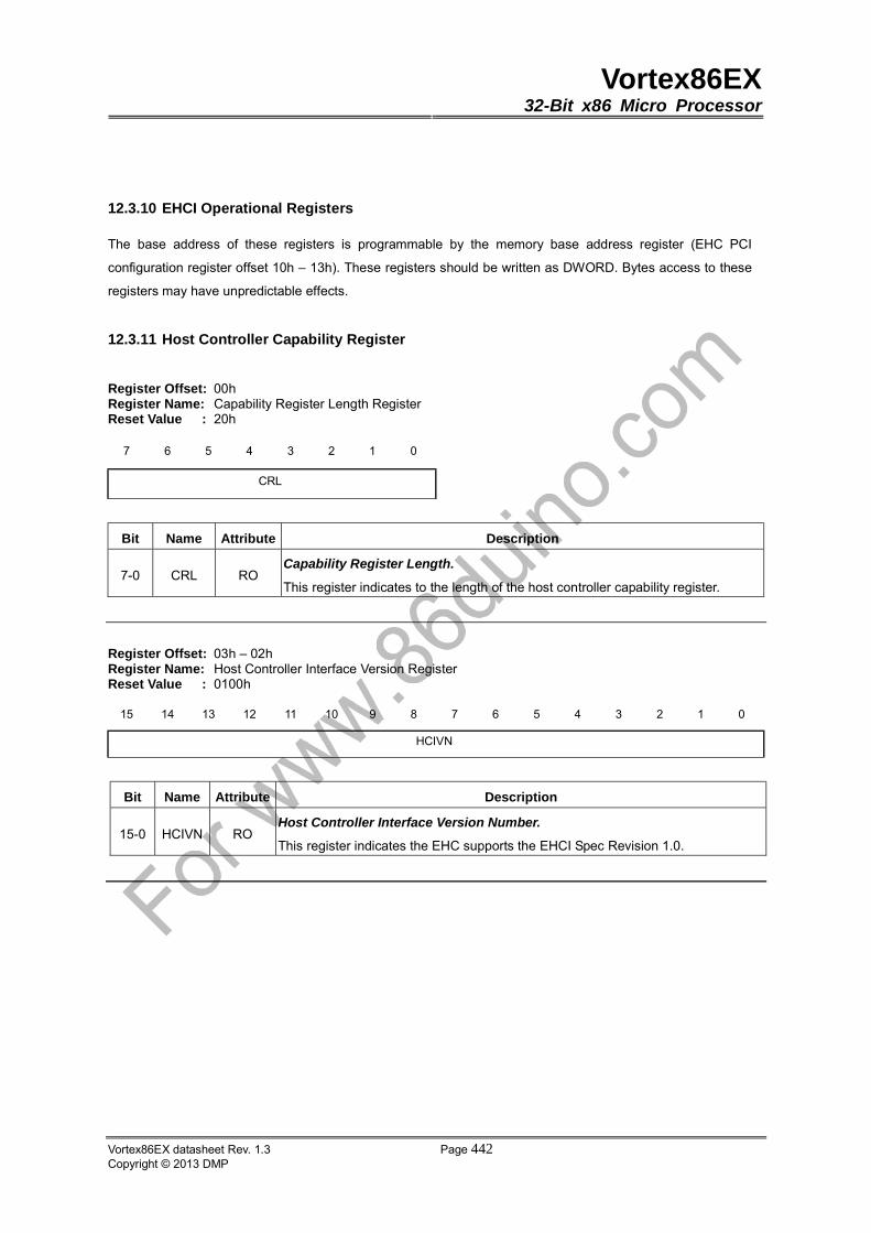
Vortex86EX32-Bit x86 Micro Processor
Vortex86EX datasheet Rev. 1.3 Page 442Copyright © 2013 DMP
12.3.10 EHCI Operational Registers
The base address of these registers is programmable by the memory base address register (EHC PCI
configuration register offset 10h – 13h). These registers should be written as DWORD. Bytes access to these
registers may have unpredictable effects.
12.3.11 Host Controller Capability Register
Register Offset: 00h Register Name: Capability Register Length Register Reset Value : 20h
7 6 5 4 3 2 1 0
CRL
Bit Name Attribute Description
7-0 CRL RO Capability Register Length.
This register indicates to the length of the host controller capability register.
Register Offset: 03h – 02h Register Name: Host Controller Interface Version Register Reset Value : 0100h
15 14 13 12 11 10 9 8 7 6 5 4 3 2 1 0
HCIVN
Bit Name Attribute Description
15-0 HCIVN RO Host Controller Interface Version Number.
This register indicates the EHC supports the EHCI Spec Revision 1.0.

Vortex86EX32-Bit x86 Micro Processor
Vortex86EX datasheet Rev. 1.3 Page 443Copyright © 2013 DMP
Register Offset: 07h – 04h Register Name: Structural Parameters Register Reset Value : 00001414h
31 30 29 28 27 26 25 24 23 22 21 20 19 18 17 16 15 14 13 12 11 10 9 8 7 6 5 4 3 2 1 0
Bit Name Attribute Description
31-24 RSVD RO Reserved. These registers are always 0.
23-20 DPN RO Debug Port Number.
This register identifies the first port as the debug port.
19-17 RSVD RO Reserved. These registers are always 0.
16 PI RO
Port Indicators (P_INDICATOR). This bit indicates whether the ports support
port indicator control. When this bit is a one, the port status and control registers
include a read/writable field for controlling the state of the port indicator.
15-12 N_CC RO
Number of Companion Controller (N_CC).
This field indicates the number of companion controllers associated with this
USB2.0 host controller.
11-8 N_PCC RO Number of Ports per Companion Controller (N_PCC).
This field indicates the number of ports supported per companion host controller.
7 PRR RO
Port Routing Rules. This field indicates the method used by this implementation
for how all ports are mapped to companion controllers. The value of this field has
the following interpretation:
Value Meaning
0 The first N_PCC ports are routed to the lowest numbered function
companion host controller, the next N_PCC port are routed to the next
lowest function companion controller, and so on.
1 The port routing is explicitly enumerated by the first N_PORTS
elements of the HCSP-PORTROUTE array.
6-5 RSVD RO Reserved. These registers are always 0.
4 PPC RO
Port Power Control (PPC). This field indicates whether the host controller
implementation includes port power control. A one in this bit indicates the ports
have port power switches. A zero in this bit indicates the port do not have port
power switches. The value of this field affects the functionality of the Port Power
field in each port status and control register.
3-0N_PORT
S RO
Number of Ports (N_PORTS).
This field indicates the number of ports supported on this host controller.

Vortex86EX32-Bit x86 Micro Processor
Vortex86EX datasheet Rev. 1.3 Page 444Copyright © 2013 DMP
Register Offset: 0Bh – 08h Register Name: Capability Parameters Register Reset Value : 00007006h
31 30 29 28 27 26 25 24 23 22 21 20 19 18 17 16 15 14 13 12 11 10 9 8 7 6 5 4 3 2 1 0
Bit Name Attribute Description
31-16 RSVD RO Reserved. These registers are always 0.
15-8 EECP RO EHCI Extend Capabilities Pointer (EECP).
This field indicates the existence of a capability list.
7-4 IST RO
Isochronous Scheduling Threshold.
This field indicates, relative to the current position of the executing host
controller, where software can reliably update the isochronous schedule.
3 RSVD RO Reserved. This register is always 0.
2 ASOC RO
Asynchronous Schedule Park Capability.
If this bit is set to a one, then the host controller supports the park feature for
high-speed queue heads in the Asynchronous Schedule.
1 PFL RO
Programmable Frame List Flag.
If this bit is set to a zero, then system software must use a frame list length of
1024 elements with this host controller. The USBCMD register Frame List Size
field is a read-only register and should be set to zero.
If set to a one, then system software can specify and use a smaller frame list and
configure the host controller via the USBCMD register Frame List Size field. The
frame list must always be aligned on a 4K page boundary. This requirement
ensures that the frame list is always physically contiguous.
0 RSVD RO Reserved. These registers are always 0.
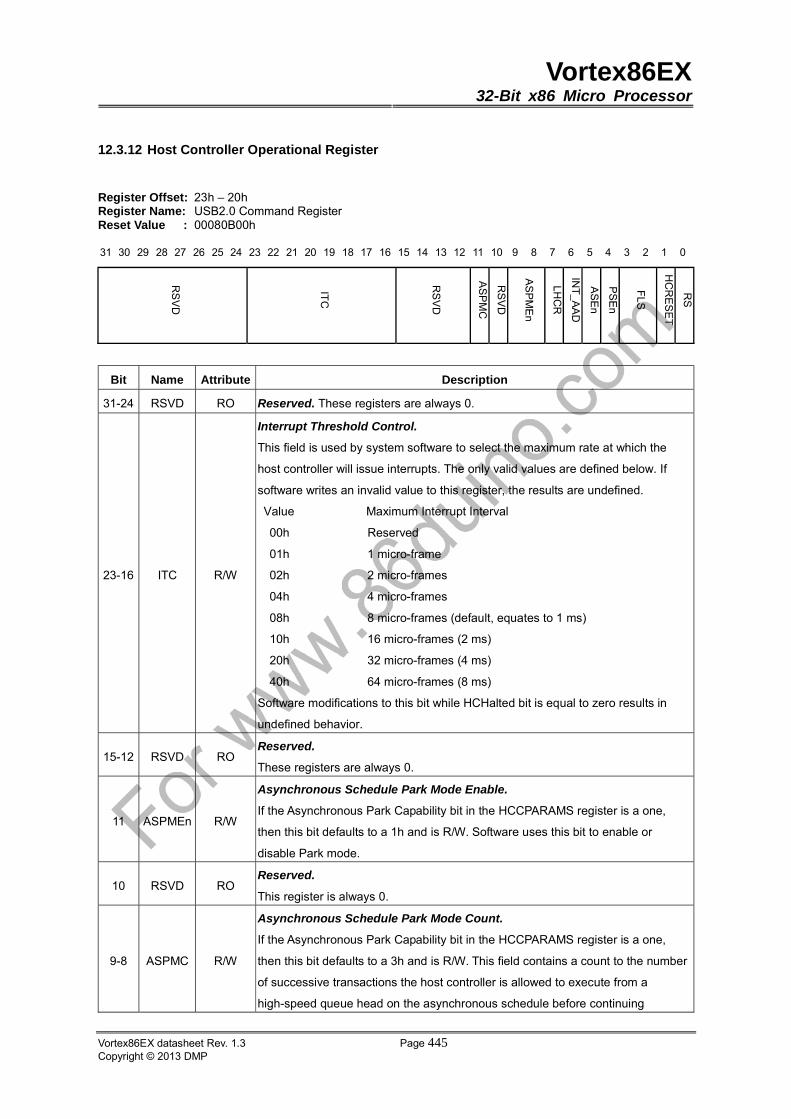
Vortex86EX32-Bit x86 Micro Processor
Vortex86EX datasheet Rev. 1.3 Page 445Copyright © 2013 DMP
12.3.12 Host Controller Operational Register
Register Offset: 23h – 20h Register Name: USB2.0 Command Register Reset Value : 00080B00h
31 30 29 28 27 26 25 24 23 22 21 20 19 18 17 16 15 14 13 12 11 10 9 8 7 6 5 4 3 2 1 0
Bit Name Attribute Description
31-24 RSVD RO Reserved. These registers are always 0.
23-16 ITC R/W
Interrupt Threshold Control.
This field is used by system software to select the maximum rate at which the
host controller will issue interrupts. The only valid values are defined below. If
software writes an invalid value to this register, the results are undefined.
Value Maximum Interrupt Interval
00h Reserved
01h 1 micro-frame
02h 2 micro-frames
04h 4 micro-frames
08h 8 micro-frames (default, equates to 1 ms)
10h 16 micro-frames (2 ms)
20h 32 micro-frames (4 ms)
40h 64 micro-frames (8 ms)
Software modifications to this bit while HCHalted bit is equal to zero results in
undefined behavior.
15-12 RSVD RO Reserved.
These registers are always 0.
11 ASPMEn R/W
Asynchronous Schedule Park Mode Enable.
If the Asynchronous Park Capability bit in the HCCPARAMS register is a one,
then this bit defaults to a 1h and is R/W. Software uses this bit to enable or
disable Park mode.
10 RSVD RO Reserved.
This register is always 0.
9-8 ASPMC R/W
Asynchronous Schedule Park Mode Count.
If the Asynchronous Park Capability bit in the HCCPARAMS register is a one,
then this bit defaults to a 3h and is R/W. This field contains a count to the number
of successive transactions the host controller is allowed to execute from a
high-speed queue head on the asynchronous schedule before continuing
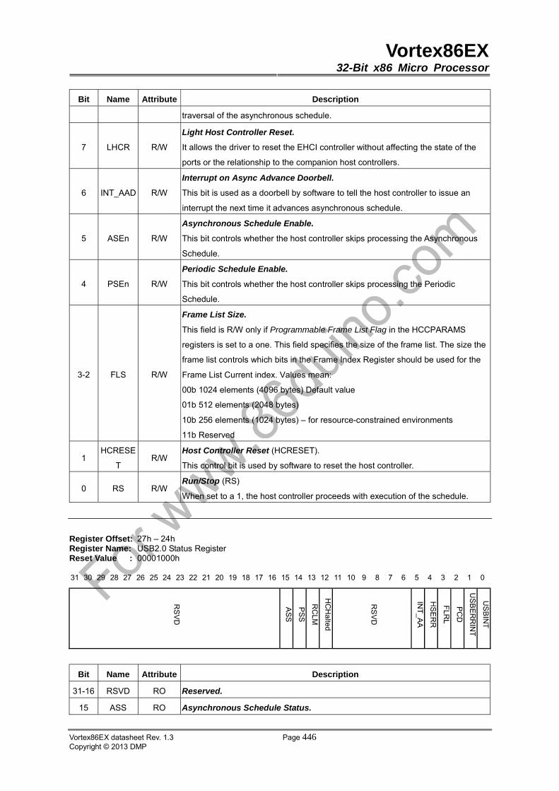
Vortex86EX32-Bit x86 Micro Processor
Vortex86EX datasheet Rev. 1.3 Page 446Copyright © 2013 DMP
Bit Name Attribute Description
traversal of the asynchronous schedule.
7 LHCR R/W
Light Host Controller Reset.
It allows the driver to reset the EHCI controller without affecting the state of the
ports or the relationship to the companion host controllers.
6 INT_AAD R/W
Interrupt on Async Advance Doorbell.
This bit is used as a doorbell by software to tell the host controller to issue an
interrupt the next time it advances asynchronous schedule.
5 ASEn R/W
Asynchronous Schedule Enable.
This bit controls whether the host controller skips processing the Asynchronous
Schedule.
4 PSEn R/W
Periodic Schedule Enable.
This bit controls whether the host controller skips processing the Periodic
Schedule.
3-2 FLS R/W
Frame List Size.
This field is R/W only if Programmable Frame List Flag in the HCCPARAMS
registers is set to a one. This field specifies the size of the frame list. The size the
frame list controls which bits in the Frame Index Register should be used for the
Frame List Current index. Values mean:
00b 1024 elements (4096 bytes) Default value
01b 512 elements (2048 bytes)
10b 256 elements (1024 bytes) – for resource-constrained environments
11b Reserved
1 HCRESE
T R/W
Host Controller Reset (HCRESET).
This control bit is used by software to reset the host controller.
0 RS R/W Run/Stop (RS)
When set to a 1, the host controller proceeds with execution of the schedule.
Register Offset: 27h – 24h Register Name: USB2.0 Status Register Reset Value : 00001000h
31 30 29 28 27 26 25 24 23 22 21 20 19 18 17 16 15 14 13 12 11 10 9 8 7 6 5 4 3 2 1 0
Bit Name Attribute Description
31-16 RSVD RO Reserved.
15 ASS RO Asynchronous Schedule Status.

Vortex86EX32-Bit x86 Micro Processor
Vortex86EX datasheet Rev. 1.3 Page 447Copyright © 2013 DMP
Bit Name Attribute Description
This bit reports the current real status of the Asynchronous Schedule. If this bit is
a zero then the status of the Asynchronous Schedule is disabled.
14 PSS RO
Periodic Schedule Status.
This bit reports the current real status of the Periodic Schedule. If this bit is a
zero then the status of the Periodic Schedule is disabled.
13 RCLM RO Reclamation.
This bit is used to detect an empty asynchronous schedule.
12 HCHalted RO
Host Controller Halted (HCHalted).
This bit is a zero whenever the Run/Stop bit is a one. The Host Controller sets
this bit to one after it has stopped executing as a result of the Run/Stop bit being
set to 0, either by software or by the Host Controller hardware.
11-6 RSVD RO Reserved.
5 INT_AA R/WC
Interrupt on Async Advance.
System software can force the host controller to issue an interrupt the next time
the host controller advances the asynchronous schedule by writing a one to the
Interrupt on Async Advance Doorbell bit in the USB2CMD register.
4 HSERR R/WC
Host System Error.
The Host Controller sets this bit to 1 when a serious error occurs during a host
system access involving the Host Controller module.
3 FLRL R/WC
Frame List Rollover.
The Host Controller sets this bit to a one when the Frame List Index rolls over
from its maximum value to zero.
2 PCD R/WC
Port Change Detect.
The Host Controller sets this bit to a one when any port for which the Port Owner
bit is set to zero has a change bit transition from a zero to a one or a Force Port
Resume bit transition from a zero to a one as a result of a J-K transaction
detected on a suspended port. This bit will also be set as a result of the Connect
Status Change being set to a one after system software has relinquished
ownership of a connected port by writing a one to a port’s Port Owner bit.
1 USBERR
INT R/WC
USB Error Interrupt (USBERRINT).
The Host Controller sets this bit to 1 when completion of a USB transaction
results in an error condition.
0 USBINT R/WC
USB Interrupt (USBINT).
The Host Controller sets this bit to 1 one the completion of a USB transaction,
which result in the retirement of a Transfer Descriptor that had its IOC bit set.

Vortex86EX32-Bit x86 Micro Processor
Vortex86EX datasheet Rev. 1.3 Page 448Copyright © 2013 DMP
Register Offset: 2Bh – 28h Register Name: USB2.0 Interrupt Enable Register Reset Value : 00000000h
31 30 29 28 27 26 25 24 23 22 21 20 19 18 17 16 15 14 13 12 11 10 9 8 7 6 5 4 3 2 1 0
Bit Name Attribute Description
31-16 RSVD RO Reserved.
5 INT_AAE
n R/W
Interrupt on Async Advance Enable.
When this bit is a one and the Interrupt on the Async Advance bit in the USBSTS
register is a one, the host controller will issue an interrupt at the next interrupt
threshold. The interrupt is acknowledged by software clearing the Interrupt on the
Async Advance bit.
4 HSERRE
n R/W
Host System Error Enable.
When this bit is a one and the Host System Error Status bit in the USBSTS
register is a one, the host controller will issue an interrupt. The interrupt is
acknowledged by software clearing the Host System Error bit.
3 FLRLEn R/W
Frame List Rollover Enable.
When the Rollover bit in the USBSTS register is a one, the host controller will
issue an interrupt. The interrupt is acknowledged by software clearing the Frame
List Rollover bit
2 PCDEn R/W
Port Change Detect Enable.
When this bit is a one and the Port Chang Detect bit in the USBSTS register is a
one, the host controller will issue an interrupt. The interrupt is acknowledged by
software clearing the Port Change Detect bit.
1 USBERR
INTEnR/W
USB Error Interrupt Enable.
When this bit is a one, and the USBERRINT bit in the USBSTS register is a one,
the host controller will issue an interrupt at the next interrupt threshold. The
interrupt is acknowledged by software clearing the USBERRINT bit.
0 USBINTE
n R/W
USB Interrupt Enable.
When this bit is a one and the USBINT bit in the USBSTS register is a one, the
host controller will issue an interrupt at the next interrupt threshold. The interrupt
is acknowledged by software clearing the USBINT bit.

Vortex86EX32-Bit x86 Micro Processor
Vortex86EX datasheet Rev. 1.3 Page 449Copyright © 2013 DMP
Register Offset: 2Fh – 2Ch Register Name: USB2.0 Frame Index Register Reset Value : 00000000h
31 30 29 28 27 26 25 24 23 22 21 20 19 18 17 16 15 14 13 12 11 10 9 8 7 6 5 4 3 2 1 0
RSVD FI
Bit Name Attribute Description
31-14 RSVD RO Reserved. These registers are always 0.
13-0 FI R/W
Frame Index.
The value in this register increments at the end of each time frame (e.g.
micro-frame). Bits [N:3] are used for the Frame List current index. This means that
each location of the frame list is accessed 8 times (frames or micro-frames)
before moving to the next index. The following illustrates values of N based on the
value of the Frame List Size field in the USBCMD register.
USBCMD[Frame List Size] Number Elements N
00b (1024) 12
01b (512) 11
10b (256) 10
11b Reserved
Register Offset: 37h – 34h Register Name: Periodic Frame List Base Address Register Reset Value : 00000000h
31 30 29 28 27 26 25 24 23 22 21 20 19 18 17 16 15 14 13 12 11 10 9 8 7 6 5 4 3 2 1 0
BA RSVD
Bit Name Attribute Description
31-12 BA R/W Base Address. These bits correspond to memory address [31:12].
11-0 RSVD RO Reserved. These registers are always 0.
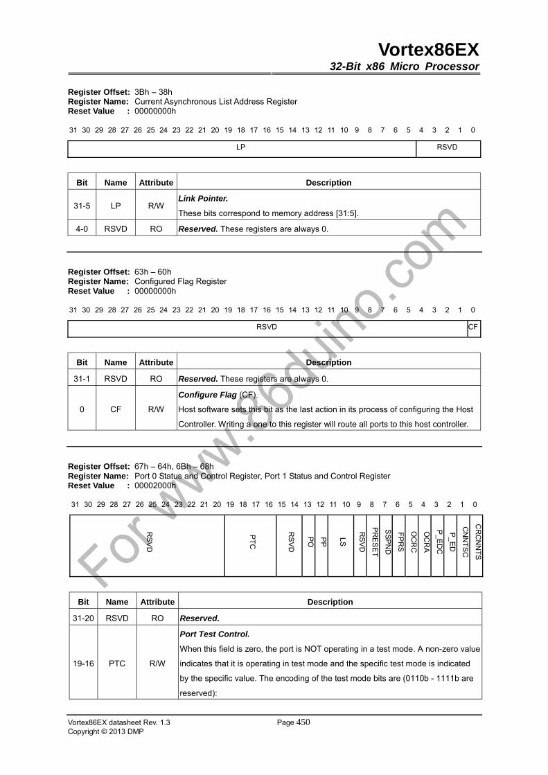
Vortex86EX32-Bit x86 Micro Processor
Vortex86EX datasheet Rev. 1.3 Page 450Copyright © 2013 DMP
Register Offset: 3Bh – 38h Register Name: Current Asynchronous List Address Register Reset Value : 00000000h
31 30 29 28 27 26 25 24 23 22 21 20 19 18 17 16 15 14 13 12 11 10 9 8 7 6 5 4 3 2 1 0
LP RSVD
Bit Name Attribute Description
31-5 LP R/W Link Pointer.
These bits correspond to memory address [31:5].
4-0 RSVD RO Reserved. These registers are always 0.
Register Offset: 63h – 60h Register Name: Configured Flag Register Reset Value : 00000000h
31 30 29 28 27 26 25 24 23 22 21 20 19 18 17 16 15 14 13 12 11 10 9 8 7 6 5 4 3 2 1 0
RSVD CF
Bit Name Attribute Description
31-1 RSVD RO Reserved. These registers are always 0.
0 CF R/W
Configure Flag (CF).
Host software sets this bit as the last action in its process of configuring the Host
Controller. Writing a one to this register will route all ports to this host controller.
Register Offset: 67h – 64h, 6Bh – 68h Register Name: Port 0 Status and Control Register, Port 1 Status and Control Register Reset Value : 00002000h
31 30 29 28 27 26 25 24 23 22 21 20 19 18 17 16 15 14 13 12 11 10 9 8 7 6 5 4 3 2 1 0
Bit Name Attribute Description
31-20 RSVD RO Reserved.
19-16 PTC R/W
Port Test Control.
When this field is zero, the port is NOT operating in a test mode. A non-zero value
indicates that it is operating in test mode and the specific test mode is indicated
by the specific value. The encoding of the test mode bits are (0110b - 1111b are
reserved):

Vortex86EX32-Bit x86 Micro Processor
Vortex86EX datasheet Rev. 1.3 Page 451Copyright © 2013 DMP
Bit Name Attribute Description
Bits Test Mode
0000b Test mode not enabled
0001b Test J_STATE
0010b Test K_STATE
0011b Test SE0_NAK
0100b Test Packet
0101b Test FORCE_ENABLE
15-14 RSVD RO Reserved.
13 PO R/W
Port Owner.
This bit unconditionally goes to a 0b when the Configured bit in the
CONFIGFLAG register makes a 0b to 1b transition. This bit unconditionally goes
to 1b whenever the Configured bit is zero. Software writes a one to this bit when
the attached device is not a high-speed device.
12 PP R/W
Port Power (PP).
The function of this bit depends on the value of the Port Power Control (PPC) field
in the HCSPARAMS register. The behavior is as follows:
PPC PP Operation
0b 1b RO Host controller does not have port power control
switches. Each port is hard-wired to power.
1b 1b/0b R/W Host controller has port power control switches. This
bit represents the current setting of the switch (0 = off, 1 =
on). When power is not available on a port (i.e. PP equals a
0), the port is nonfunctional and will not report attaches,
detaches, etc.
When an over-current condition is detected on a powered port and PPC is a
one, the PP bit in each affected port may be transitioned by the host controller
from a 1 to 0 (removing power from the port).
11-10 LS RO
Line Status.
These bits reflect the current logical levels of the D+ (bit 11) and D- (bit 10) signal
lines.
9 RSVD RO Reserved. This bit is always 0.
8 PRESET R/W
Port Reset.
When software writes a one to this bit, the bus reset sequence as defined in the
USB Spec Revision 2.0 is started. Software writes a zero to this bit to terminate
the bus reset sequence.
7 SSPND R/W
Suspend.
Software writes a one to this bit to suspend the downstream port. A write of zero
to this bit is ignored by the host controller. The host controller will unconditionally
set this bit to a zero when software sets the Force Port Resume from 1 to 0 or
sets the Port Reset bit to 1.
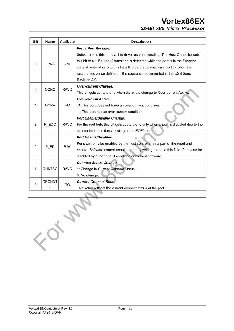
Vortex86EX32-Bit x86 Micro Processor
Vortex86EX datasheet Rev. 1.3 Page 452Copyright © 2013 DMP
Bit Name Attribute Description
6 FPRS R/W
Force Port Resume.
Software sets this bit to a 1 to drive resume signaling. The Host Controller sets
this bit to a 1 if a J-to-K transition is detected while the port is in the Suspend
state. A write of zero to this bit will force the downstream port to follow the
resume sequence defined in the sequence documented in the USB Spec
Revision 2.0.
5 OCRC R/WC Over-current Change.
This bit gets set to a one when there is a change to Over-current Active.
4 OCRA RO
Over-current Active.
0: This port does not have an over-current condition.
1: This port has an over-current condition.
3 P_EDC R/WC
Port Enable/Disable Change.
For the root hub, this bit gets set to a one only when a port is disabled due to the
appropriate conditions existing at the EOF2 pointer.
2 P_ED R/W
Port Enable/Disabled.
Ports can only be enabled by the host controller as a part of the reset and
enable. Software cannot enable a port by writing a one to this field. Ports can be
disabled by either a fault condition or by host software.
1 CNNTSC R/WC
Connect Status Change.
1: Change in Current Connect Status.
0: No change.
0 CRCNNT
S RO
Current Connect Status.
This value reflects the current connect status of the port.
Vortex86EX32-Bit x86 Micro Processor
Vortex86EX datasheet Rev. 1.3 Page 453Copyright © 2013 DMP
13. SD/SATA Controller
13.1 Overview
The IDE to SD/SATA controller, which is compatible with the ATA/ATAPI-6 specification .It supports
not only a Scatter/Gather DMA mechanism that complies with the Programming Interface for Bus
Master IDE Controller Revision 1.0 but also 2 IDE channels and primariy channel for SD, secondary
for SATA..
13.2 Features
� IDE Functions
– Compatible with the ATA/ATAPI-6 specification and supports two IDE channels. (primariy
channel for SD, secondary for SATA)
– Supports ANSI ATA proposal PIO Modes 0, 1, 2, 3, 4 with flow control, DMA Modes 0, 1, 2
and Ultra DMA modes 0, 1, 2, 3, 4, 5, 6
– Programmable active pulses and recovery time for data port access timing
– 512 bytes FIFO for data transfer per IDE channel
– Supports Scatter/Gather function for DMA/UDMA transfer
– Supports pre-fetch and post-write function for PIO mode per IDE channe
� PCI Interface
– Host interface compiles with PCI local bus specification revision 2.2
– Supports PCI Power Management v1.1 capability
– Support one Flash/ROM interface for expansion ROM of PCI card

Vortex86EX32-Bit x86 Micro Processor
Vortex86EX datasheet Rev. 1.3 Page 454Copyright © 2013 DMP
13.3 List of PCI Configuration Registers
31 16 15 00 Index
Device ID (1012h) Vendor ID (17F3h) 00h-03h
Status (0200h) Command (0000h) 04h-07h
Base Class Code
(01h)
Sub-class code
(01h)
Program Interface
(8Ah) Revision ID (03h) 08h-0Bh
Reserved Header Type (00h)Latency Timer
(00h)
Cache Line Size
(08h) 0Ch-0Fh
Primary Channel Command Block Register Base Address (00000001h) 10h-13h
Primary channel Control Block Register Base Address (00000001h) 14h-17h
Secondary Channel Command Block Register Base Address (00000001h) 18h-1Bh
Secondary Channel Control Block Register Base Address (00000001h) 1Ch-1Fh
Bus Master Base Address Register (00000001h) 20h-23h
Reserved 24h-2Bh
Sub-system Device ID (1012h) Sub-system Vendor ID (17F3h) 2Ch-2Fh
Reserved 30h-3Bh
MAX_LAT (00h) MIN_GNT (00h) INTERRUPT PIN
(01h)
INTERRUPT LINE
(FFh) 3Ch-3Fh
ATA TIMING(Secondary) ATA TIMING(Primary) 40h-43h
Reserved Reserved Reserved
Device 1 ATA
Timing(Primary
and Secondary)
44h-47h
Ultra DMA Timing Register Reserved Ultra DMA Control
Register 48h-4Bh
Reserved 4Ch-53h
Reserved IDE IO Configuration 54h-57h
Reserved 58h-5Fh
Controller Feature Register 60h-63h
Reserved 64h-7Fh
Reserved 80h-83h
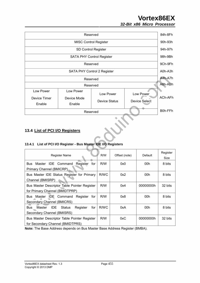
Vortex86EX32-Bit x86 Micro Processor
Vortex86EX datasheet Rev. 1.3 Page 455Copyright © 2013 DMP
Reserved 84h-8Fh
MISC Control Register 90h-93h
SD Control Register 94h-97h
SATA PHY Control Register 98h-9Bh
Reserved 9Ch-9Fh
SATA PHY Control 2 Register A0h-A3h
Reserved A4h-A7h
Reserved A8h-ABh
Low Power
Device Timer
Enable
Low Power
Device Mode
Enable
Low Power
Device Status
Low Power
Device Select ACh-AFh
Reserved B0h-FFh
13.4 List of PCI I/O Registers
13.4.1 List of PCI I/O Register - Bus Master IDE I/O Registers
Register Name R/W Offset (note) Default Register
Size
Bus Master IDE Command Register for
Primary Channel (BMICRP)
R/W 0x0 00h 8 bits
Bus Master IDE Status Register for Primary
Channel (BMISRP)
R/WC 0x2 00h 8 bits
Bus Master Descriptor Table Pointer Register
for Primary Channel (BMIDTPRP)
R/W 0x4 00000000h 32 bits
Bus Master IDE Command Register for
Secondary Channel (BMICRS)
R/W 0x8 00h 8 bits
Bus Master IDE Status Register for
Secondary Channel (BMISRS)
R/WC 0xA 00h 8 bits
Bus Master Descriptor Table Pointer Register
for Secondary Channel (BMIDTPRS)
R/W 0xC 00000000h 32 bits
Note: The Base Address depends on Bus Master Base Address Register (BMBA).

Vortex86EX32-Bit x86 Micro Processor
Vortex86EX datasheet Rev. 1.3 Page 456Copyright © 2013 DMP
13.4.2 IDE Interface and Status Registers from PCI I/O View (PCI IO Space Mapping)
Register Name R/W Offset Default Register
Size
Primary IDE Data Register (VPDR) R/W 0x0 (Note 1) 0000h 16 bits
Primary IDE Error/Feature Register (VPEFR) R/W 0x1(Note 1) 00h 8 bits
Primary IDE Sector Count (Ext) Register
(VPSCR)
R/W 0x2 (Note 1, 5) 00h 8 bits
Primary IDE Sector Number (Ext) Register
(VPSNR)
R/W 0x3 (Note 1, 5) 00h 8 bits
Primary IDE Cylinder Low (Ext) Register
(VPCLR)
R/W 0x4 (Note 1, 5) 00h 8 bits
Primary IDE Cylinder High (Ext) Register
(VPCHR)
R/W 0x5 (Note1, 5) 00h 8 bits
Primary IDE Device/Head Register (VPHDR) R/W 0x6 (Note1) 00h 8 bits
Primary IDE Command/Status Register
(VPCMR)
R/W 0x7 (Note1) 00h 8 bits
Primary IDE Device Control/Alternate Status
Register (VPSTUR)
R/W 0x6 (Note2) -- 8 bits
Secondary IDE Data Register (VSDR) R/W 0x0 (Note3) 0000h 16 bits
Secondary IDE Error/Feature Register
(VSEFR)
R/W 0x1 (Note3) 00h 8 bits
Secondary IDE Sector Count (Ext) Register
(VSSCR)
R/W 0x2 (Note 3, 5) 00h 8 bits
Secondary IDE Sector Number (Ext) Register
(VSSNR)
R/W 0x3 (Note 3, 5) 00h 8 bits
Secondary IDE Cylinder Low (Ext) Register
(VSCLR)
R/W 0x4 (Note 3, 5) 00h 8 bits
Secondary IDE Cylinder High (Ext) Register
(VSCHR)
R/W 0x5 (Note 3, 5) 00h 8 bits
Secondary IDE Device/Head Register
(VSHDR)
R/W 0x6 (Note 3) 00h 8 bits
Secondary IDE Command /Status Register
(VSCMR)
R/W 0x7 (Note 3) 00h 8 bits

Vortex86EX32-Bit x86 Micro Processor
Vortex86EX datasheet Rev. 1.3 Page 457Copyright © 2013 DMP
Secondary IDE Device Control/Alternate
Status Register (VSSTUR)
R/W 0x6 (Note4) -- 8 bits
Definition of R/W Attributes:
RO READ ONLY. If a register is read only, writing will have no effect.
R/W READ/WRITE. A register with this attribute can be read and written.
R/W1 READ/WRITE ONCE. A register with this attribute can be read and write once.
R/WC READ/WRITE CLEAR. A register bit with this attribute can be read and written. However, a
write of 1 clears the corresponding bit and a write of 0 will have no effect.
13.5 PCI Configuration Registers Definition
Register Offset: 00h Register Name: Vendor ID Register Reset Value : 17F3h
15 14 13 12 11 10 9 8 7 6 5 4 3 2 1 0
VID
Bit Name Attribute Description
15-0 VID RO Vendor ID.
Register Offset: 02h Register Name: Device ID Register Reset Value : 17F3h
15 14 13 12 11 10 9 8 7 6 5 4 3 2 1 0
DID
Bit Name Attribute Description
15-0 DID RO Device ID.

Vortex86EX32-Bit x86 Micro Processor
Vortex86EX datasheet Rev. 1.3 Page 458Copyright © 2013 DMP
Register Offset: 04h Register Name: Command Register Reset Value : 0000h
15 14 13 12 11 10 9 8 7 6 5 4 3 2 1 0
RSVD PER RSVD DBME RSVD IOAE
Bit Name Attribute Description
15-7 RSVD RO Reserved.
6 PER RO
Parity Error Response.
1: Enabled
0: Disabled
5-3 RSVD RO Reserved.
2 DBME RW
DMA Bus Master Enable.
1: Enabled
0: Disabled
1 RSVD RO Reserved.
0 IOAE RW
I/O Access Enable.
1: Allow the chip to respond to I/O space accesses.
0: Disable I/O space accesses.
Register Offset: 06h Register Name: Device Status Register Reset Value : 630h
15 14 13 12 11 10 9 8 7 6 5 4 3 2 1 0
RSVD PER RSVD DBME RSVD IOAE
Bit Name Attribute Description
15-14 RSVD RO Reserved.
13 MAST R/WC
Master Abort Status.
This bit is set to high when the IDE Controller acts as a PCI master and has
issued a Master-Abort.
Write 1 to clear this bit.
12 RTA R/WC
Received Target Abort.
This bit is set to high when the IDE controller is a PCI master and the PCI
transaction is terminated by receiving a Target-Abort.
Write 1 to clear this bit.
11 RSVD RO Reserved.
10-9 DEVT[1:0] RO
DEVSEL Timing.
Medium timing is selected for DEVSEL# assertion when the PCI target performs
the positive decode.

Vortex86EX32-Bit x86 Micro Processor
Vortex86EX datasheet Rev. 1.3 Page 459Copyright © 2013 DMP
8 RSVD RO Reserved.
7 FBC RO
Fast Back-to-Back Capable.
Always read as 0.
Not supported.
6 RSVD RO Reserved.
5 CAB-66 RO
66 MHz Capable.
A “1” indicates that the function supports 66 MHz.
A “0” indicates that the function just supports 33 MHz.
4 CAP RO
Capabilities.
This bit indicates whether this function implements a list of extended capabilities
such as the PCI power management. When being set, it indicates the presence of
capabilities. The value of “0” means that this function does not implement
capabilities.
3-0 RSVD RO Reserved.
Register Offset: 08h Register Name: Revision Register Reset Value: 03h
7 6 5 4 3 2 1 0
RID
Bit Name Attribute Description
7-0 RID RO Revision ID.
The revision number of the IDE controller.
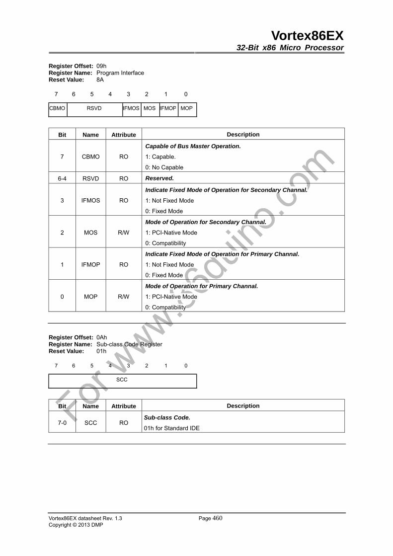
Vortex86EX32-Bit x86 Micro Processor
Vortex86EX datasheet Rev. 1.3 Page 460Copyright © 2013 DMP
Register Offset: 09h Register Name: Program Interface Reset Value: 8A
7 6 5 4 3 2 1 0
CBMO RSVD IFMOS MOS IFMOP MOP
Bit Name Attribute Description
7 CBMO RO
Capable of Bus Master Operation.
1: Capable.
0: No Capable
6-4 RSVD RO Reserved.
3 IFMOS RO
Indicate Fixed Mode of Operation for Secondary Channal.
1: Not Fixed Mode
0: Fixed Mode
2 MOS R/W
Mode of Operation for Secondary Channal.
1: PCI-Native Mode
0: Compatibility
1 IFMOP RO
Indicate Fixed Mode of Operation for Primary Channal.
1: Not Fixed Mode
0: Fixed Mode
0 MOP R/W
Mode of Operation for Primary Channal.
1: PCI-Native Mode
0: Compatibility
Register Offset: 0Ah Register Name: Sub-class Code Register Reset Value: 01h
7 6 5 4 3 2 1 0
SCC
Bit Name Attribute Description
7-0 SCC RO Sub-class Code.
01h for Standard IDE
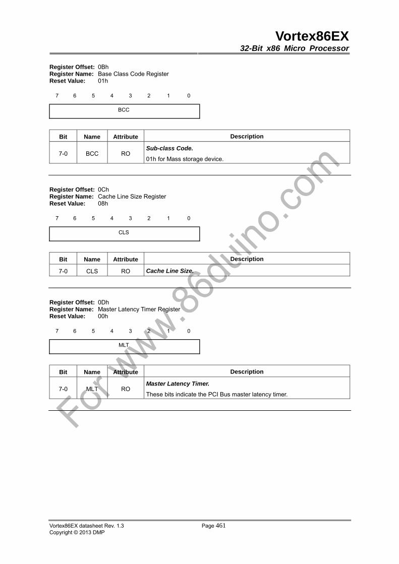
Vortex86EX32-Bit x86 Micro Processor
Vortex86EX datasheet Rev. 1.3 Page 461Copyright © 2013 DMP
Register Offset: 0Bh Register Name: Base Class Code Register Reset Value: 01h
7 6 5 4 3 2 1 0
BCC
Bit Name Attribute Description
7-0 BCC RO Sub-class Code.
01h for Mass storage device.
Register Offset: 0Ch Register Name: Cache Line Size Register Reset Value: 08h
7 6 5 4 3 2 1 0
CLS
Bit Name Attribute Description
7-0 CLS RO Cache Line Size.
Register Offset: 0Dh Register Name: Master Latency Timer Register Reset Value: 00h
7 6 5 4 3 2 1 0
MLT
Bit Name Attribute Description
7-0 MLT RO Master Latency Timer.
These bits indicate the PCI Bus master latency timer.
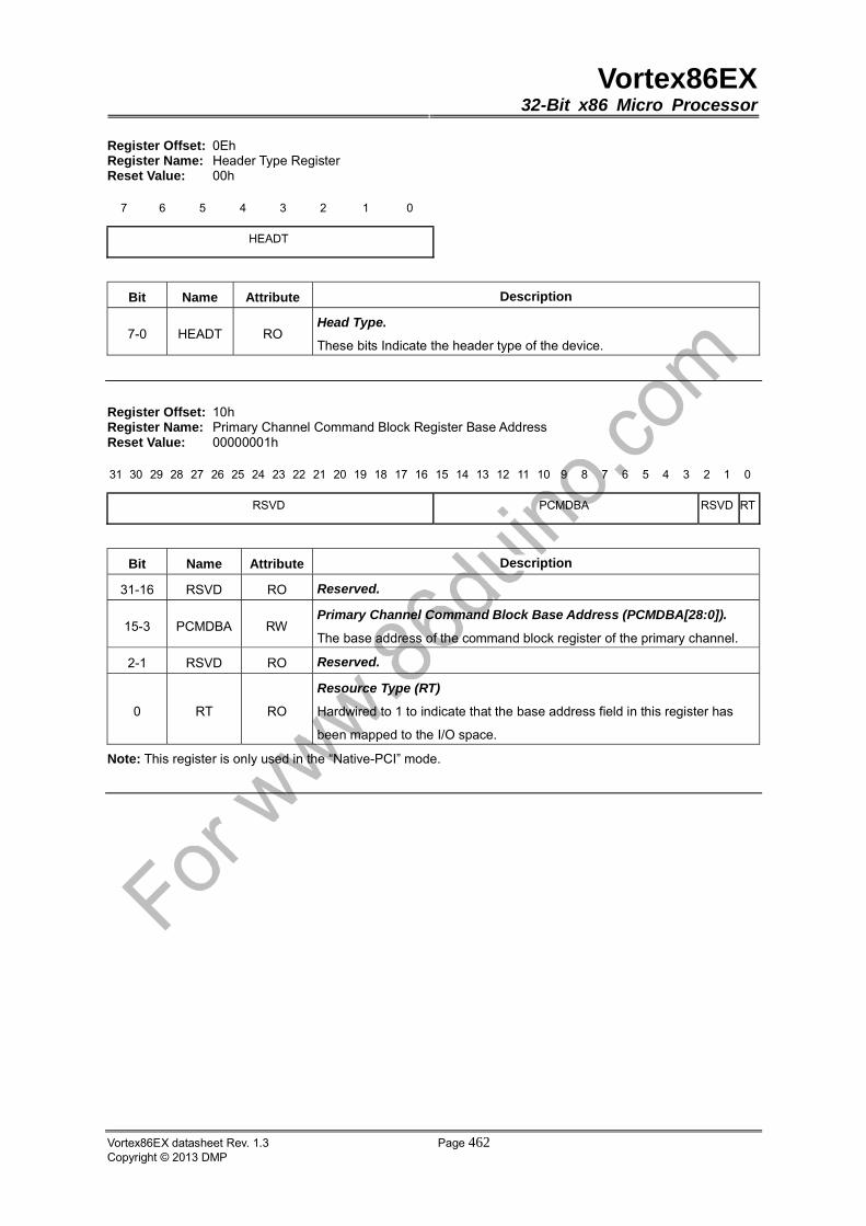
Vortex86EX32-Bit x86 Micro Processor
Vortex86EX datasheet Rev. 1.3 Page 462Copyright © 2013 DMP
Register Offset: 0Eh Register Name: Header Type Register Reset Value: 00h
7 6 5 4 3 2 1 0
HEADT
Bit Name Attribute Description
7-0 HEADT RO Head Type.
These bits Indicate the header type of the device.
Register Offset: 10h Register Name: Primary Channel Command Block Register Base Address Reset Value: 00000001h
31 30 29 28 27 26 25 24 23 22 21 20 19 18 17 16 15 14 13 12 11 10 9 8 7 6 5 4 3 2 1 0
RSVD PCMDBA RSVD RT
Bit Name Attribute Description
31-16 RSVD RO Reserved.
15-3 PCMDBA RW Primary Channel Command Block Base Address (PCMDBA[28:0]).
The base address of the command block register of the primary channel.
2-1 RSVD RO Reserved.
0 RT RO
Resource Type (RT)
Hardwired to 1 to indicate that the base address field in this register has
been mapped to the I/O space.
Note: This register is only used in the “Native-PCI” mode.
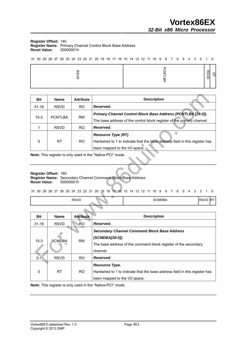
Vortex86EX32-Bit x86 Micro Processor
Vortex86EX datasheet Rev. 1.3 Page 463Copyright © 2013 DMP
Register Offset: 14h Register Name: Primary Channel Control Block Base Address Reset Value: 00000001h
31 30 29 28 27 26 25 24 23 22 21 20 19 18 17 16 15 14 13 12 11 10 9 8 7 6 5 4 3 2 1 0
Bit Name Attribute Description
31-16 RSVD RO Reserved.
15-2 PCNTLBA RW Primary Channel Control Block Base Address (PCNTLBA [29:0]).
The base address of the control block register of the primary channel.
1 RSVD RO Reserved.
0 RT RO
Resource Type (RT)
Hardwired to 1 to indicate that the base address field in this register has
been mapped to the I/O space.
Note: This register is only used in the “Native-PCI” mode.
Register Offset: 18h Register Name: Secondary Channel Command Block Base Address Reset Value: 00000001h
31 30 29 28 27 26 25 24 23 22 21 20 19 18 17 16 15 14 13 12 11 10 9 8 7 6 5 4 3 2 1 0
RSVD SCMDBA RSVD RT
Bit Name Attribute Description
31-16 RSVD RO Reserved.
15-3 SCMDBA RW
Secondary Channel Command Block Base Address
(SCMDBA[28:0]).
The base address of the command block register of the secondary
channel.
2-1 RSVD RO Reserved.
0 RT RO
Resource Type.
Hardwired to 1 to indicate that the base address field in this register has
been mapped to the I/O space.
Note: This register is only used in the “Native-PCI” mode.
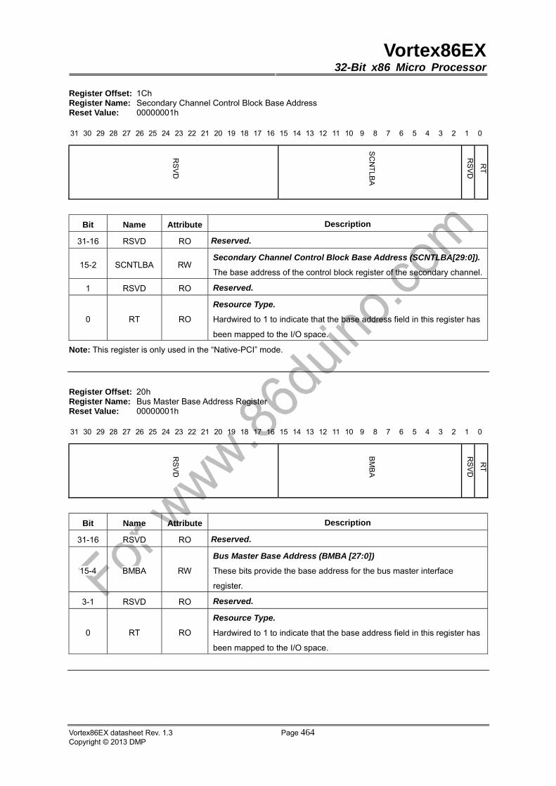
Vortex86EX32-Bit x86 Micro Processor
Vortex86EX datasheet Rev. 1.3 Page 464Copyright © 2013 DMP
Register Offset: 1Ch Register Name: Secondary Channel Control Block Base Address Reset Value: 00000001h
31 30 29 28 27 26 25 24 23 22 21 20 19 18 17 16 15 14 13 12 11 10 9 8 7 6 5 4 3 2 1 0
Bit Name Attribute Description
31-16 RSVD RO Reserved.
15-2 SCNTLBA RW Secondary Channel Control Block Base Address (SCNTLBA[29:0]).
The base address of the control block register of the secondary channel.
1 RSVD RO Reserved.
0 RT RO
Resource Type.
Hardwired to 1 to indicate that the base address field in this register has
been mapped to the I/O space.
Note: This register is only used in the “Native-PCI” mode.
Register Offset: 20h Register Name: Bus Master Base Address Register Reset Value: 00000001h
31 30 29 28 27 26 25 24 23 22 21 20 19 18 17 16 15 14 13 12 11 10 9 8 7 6 5 4 3 2 1 0
Bit Name Attribute Description
31-16 RSVD RO Reserved.
15-4 BMBA RW
Bus Master Base Address (BMBA [27:0])
These bits provide the base address for the bus master interface
register.
3-1 RSVD RO Reserved.
0 RT RO
Resource Type.
Hardwired to 1 to indicate that the base address field in this register has
been mapped to the I/O space.
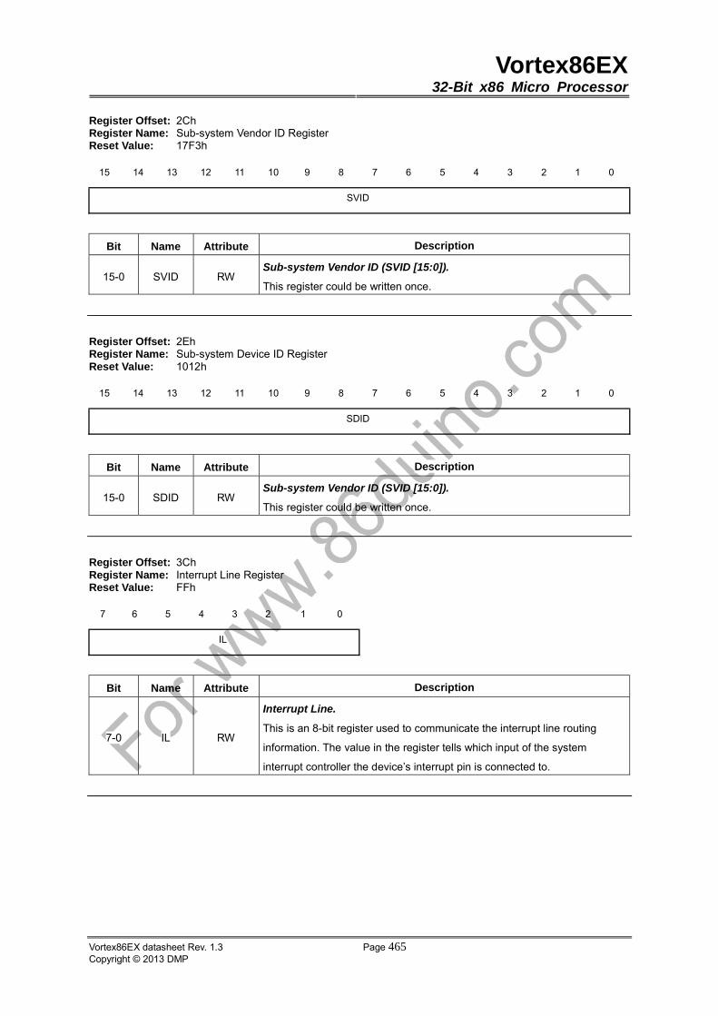
Vortex86EX32-Bit x86 Micro Processor
Vortex86EX datasheet Rev. 1.3 Page 465Copyright © 2013 DMP
Register Offset: 2Ch Register Name: Sub-system Vendor ID Register Reset Value: 17F3h
15 14 13 12 11 10 9 8 7 6 5 4 3 2 1 0
SVID
Bit Name Attribute Description
15-0 SVID RW Sub-system Vendor ID (SVID [15:0]).
This register could be written once.
Register Offset: 2Eh Register Name: Sub-system Device ID Register Reset Value: 1012h
15 14 13 12 11 10 9 8 7 6 5 4 3 2 1 0
SDID
Bit Name Attribute Description
15-0 SDID RW Sub-system Vendor ID (SVID [15:0]).
This register could be written once.
Register Offset: 3Ch Register Name: Interrupt Line Register Reset Value: FFh
7 6 5 4 3 2 1 0
IL
Bit Name Attribute Description
7-0 IL RW
Interrupt Line.
This is an 8-bit register used to communicate the interrupt line routing
information. The value in the register tells which input of the system
interrupt controller the device’s interrupt pin is connected to.

Vortex86EX32-Bit x86 Micro Processor
Vortex86EX datasheet Rev. 1.3 Page 466Copyright © 2013 DMP
Register Offset: 3Dh Register Name: Interrupt Pin Register Reset Value: 01h
7 6 5 4 3 2 1 0
IP
Bit Name Attribute Description
7-0 IP RO
Interrupt Pin.
The register tells which interrupt pin the device uses. The device only uses
the INTA#, so the value is 01h.
Register Offset: 3Eh Register Name: MIN_GNT Register Reset Value: 00h
7 6 5 4 3 2 1 0
MG
Bit Name Attribute Description
7-0 MG RO MIN_GNT.
The device has requirements for the setting of Latency Timers.
Register Offset: 3Fh Register Name: MAX_LAT Register Reset Value: 00h
7 6 5 4 3 2 1 0
ML
Bit Name Attribute Description
7-0 ML RO MAX_LAT.
The device has requirements for the setting of Latency Timers.
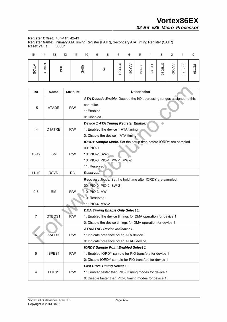
Vortex86EX32-Bit x86 Micro Processor
Vortex86EX datasheet Rev. 1.3 Page 467Copyright © 2013 DMP
Register Offset: 40h-41h, 42-43 Register Name: Primary ATA Timing Register (PATR), Secondary ATA Timing Register (SATR) Reset Value: 0000h
15 14 13 12 11 10 9 8 7 6 5 4 3 2 1 0
Bit Name Attribute Description
15 ATADE R/W
ATA Decode Enable. Decode the I/O addressing ranges assigned to this
controller.
1: Enabled.
0: Disabled.
14 D1ATRE R/W
Device 1 ATA Timing Register Enable.
1: Enabled the device 1 ATA timing.
0: Disable the device 1 ATA timing
13-12 ISM R/W
IORDY Sample Mode. Set the setup time before IORDY are sampled.
00: PIO-0
10: PIO-2, SW-2
10: PIO-3, PIO-4, MW-1, MW-2
11: Reserved
11-10 RSVD RO Reserved.
9-8 RM R/W
Recovery Mode. Set the hold time after IORDY are sampled.
00: PIO-0, PIO-2, SW-2
10: PIO-3, MW-1
10: Reserved
11: PIO-4, MW-2
7 DTEOS1 R/W
DMA Timing Enable Only Select 1.
1: Enabled the device timings for DMA operation for device 1
0: Disable the device timings for DMA operation for device 1
6 AAPDI1 R/W
ATA/ATAPI Device Indicator 1.
1: Indicate presence od an ATA device
0: Indicate presence od an ATAPI device
5 ISPES1 R/W
IORDY Sample Point Enabled Select 1.
1: Enabled IORDY sample for PIO transfers for device 1
0: Disable IORDY sample for PIO transfers for device 1
4 FDTS1 R/W
Fast Drive Timing Select 1.
1: Enabled faster than PIO-0 timing modes for device 1
0: Disable faster than PIO-0 timing modes for device 1
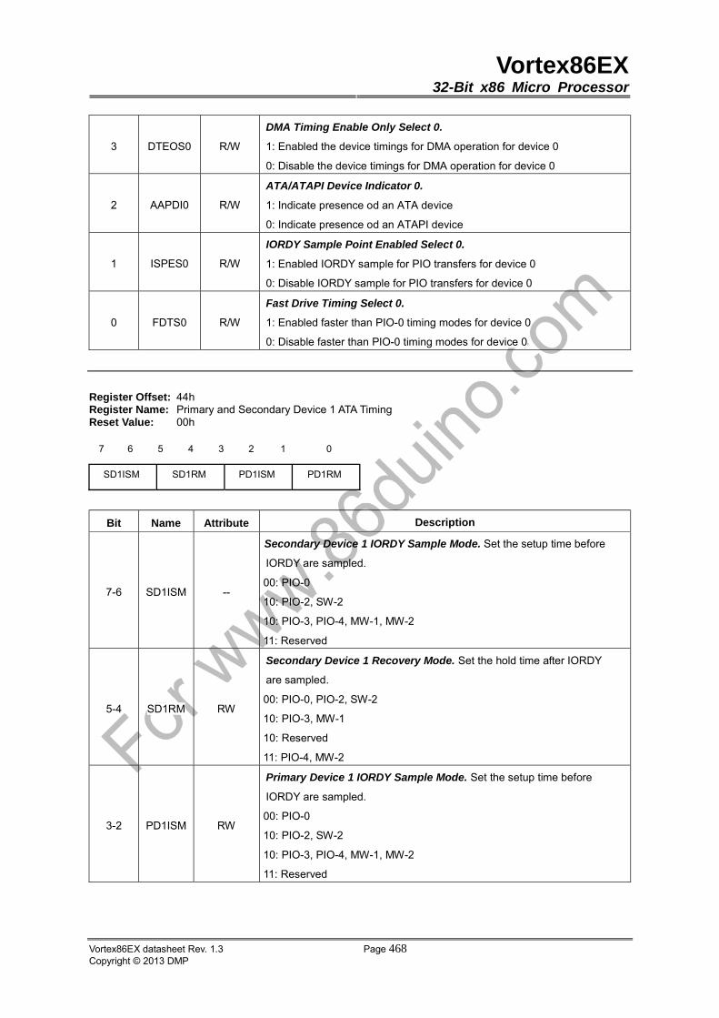
Vortex86EX32-Bit x86 Micro Processor
Vortex86EX datasheet Rev. 1.3 Page 468Copyright © 2013 DMP
3 DTEOS0 R/W
DMA Timing Enable Only Select 0.
1: Enabled the device timings for DMA operation for device 0
0: Disable the device timings for DMA operation for device 0
2 AAPDI0 R/W
ATA/ATAPI Device Indicator 0.
1: Indicate presence od an ATA device
0: Indicate presence od an ATAPI device
1 ISPES0 R/W
IORDY Sample Point Enabled Select 0.
1: Enabled IORDY sample for PIO transfers for device 0
0: Disable IORDY sample for PIO transfers for device 0
0 FDTS0 R/W
Fast Drive Timing Select 0.
1: Enabled faster than PIO-0 timing modes for device 0
0: Disable faster than PIO-0 timing modes for device 0
Register Offset: 44h Register Name: Primary and Secondary Device 1 ATA Timing Reset Value: 00h
7 6 5 4 3 2 1 0
SD1ISM SD1RM PD1ISM PD1RM
Bit Name Attribute Description
7-6 SD1ISM --
Secondary Device 1 IORDY Sample Mode. Set the setup time before
IORDY are sampled.
00: PIO-0
10: PIO-2, SW-2
10: PIO-3, PIO-4, MW-1, MW-2
11: Reserved
5-4 SD1RM RW
Secondary Device 1 Recovery Mode. Set the hold time after IORDY
are sampled.
00: PIO-0, PIO-2, SW-2
10: PIO-3, MW-1
10: Reserved
11: PIO-4, MW-2
3-2 PD1ISM RW
Primary Device 1 IORDY Sample Mode. Set the setup time before
IORDY are sampled.
00: PIO-0
10: PIO-2, SW-2
10: PIO-3, PIO-4, MW-1, MW-2
11: Reserved
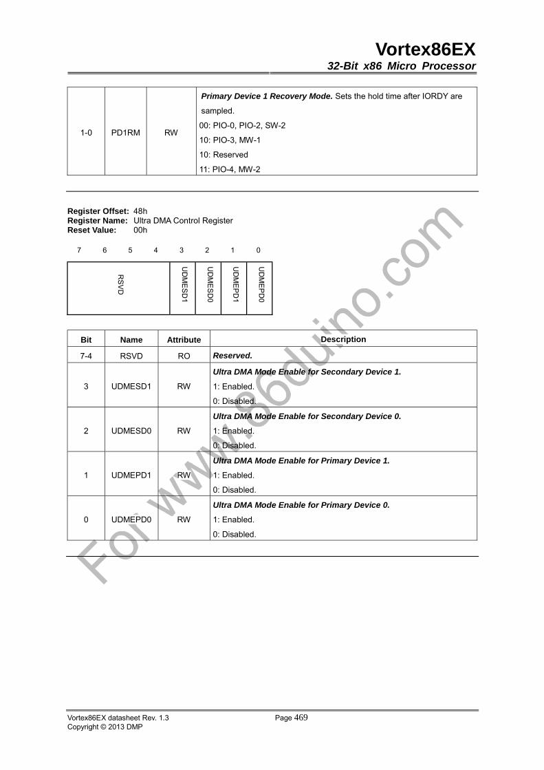
Vortex86EX32-Bit x86 Micro Processor
Vortex86EX datasheet Rev. 1.3 Page 469Copyright © 2013 DMP
1-0 PD1RM RW
Primary Device 1 Recovery Mode. Sets the hold time after IORDY are
sampled.
00: PIO-0, PIO-2, SW-2
10: PIO-3, MW-1
10: Reserved
11: PIO-4, MW-2
Register Offset: 48h Register Name: Ultra DMA Control Register Reset Value: 00h
7 6 5 4 3 2 1 0
Bit Name Attribute Description
7-4 RSVD RO Reserved.
3 UDMESD1 RW
Ultra DMA Mode Enable for Secondary Device 1.
1: Enabled.
0: Disabled.
2 UDMESD0 RW
Ultra DMA Mode Enable for Secondary Device 0.
1: Enabled.
0: Disabled.
1 UDMEPD1 RW
Ultra DMA Mode Enable for Primary Device 1.
1: Enabled.
0: Disabled.
0 UDMEPD0 RW
Ultra DMA Mode Enable for Primary Device 0.
1: Enabled.
0: Disabled.
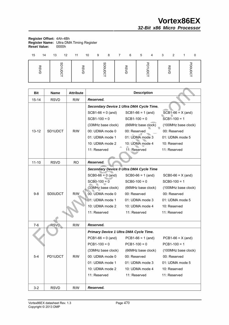
Vortex86EX32-Bit x86 Micro Processor
Vortex86EX datasheet Rev. 1.3 Page 470Copyright © 2013 DMP
Register Offset: 4Ah-4Bh Register Name: Ultra DMA Timing Register Reset Value: 0000h
15 14 13 12 11 10 9 8 7 6 5 4 3 2 1 0
Bit Name Attribute Description
15-14 RSVD R/W Reserved.
13-12 SD1UDCT R/W
Secondary Device 1 Ultra DMA Cycle Time.
SCB1-66 = 0 (and) SCB1-66 = 1 (and) SCB1-66 = X (and)
SCB1-100 = 0 SCB1-100 = 0 SCB1-100 = 1
(33MHz base clock) (66MHz base clock) (100MHz base clock)
00: UDMA mode 0 00: Reserved 00: Reserved
01: UDMA mode 1 01: UDMA mode 3 01: UDMA mode 5
10: UDMA mode 2 10: UDMA mode 4 10: Reserved
11: Reserved 11: Reserved 11: Reserved
11-10 RSVD RO Reserved.
9-8 SD0UDCT R/W
Secondary Device 0 Ultra DMA Cycle Time
SCB0-66 = 0 (and) SCB0-66 = 1 (and) SCB0-66 = X (and)
SCB0-100 = 0 SCB0-100 = 0 SCB0-100 = 1
(33MHz base clock) (66MHz base clock) (100MHz base clock)
00: UDMA mode 0 00: Reserved 00: Reserved
01: UDMA mode 1 01: UDMA mode 3 01: UDMA mode 5
10: UDMA mode 2 10: UDMA mode 4 10: Reserved
11: Reserved 11: Reserved 11: Reserved
7-6 RSVD R/W Reserved.
5-4 PD1UDCT R/W
Primary Device 1 Ultra DMA Cycle Time.
PCB1-66 = 0 (and) PCB1-66 = 1 (and) PCB1-66 = X (and)
PCB1-100 = 0 PCB1-100 = 0 PCB1-100 = 1
(33MHz base clock) (66MHz base clock) (100MHz base clock)
00: UDMA mode 0 00: Reserved 00: Reserved
01: UDMA mode 1 01: UDMA mode 3 01: UDMA mode 5
10: UDMA mode 2 10: UDMA mode 4 10: Reserved
11: Reserved 11: Reserved 11: Reserved
3-2 RSVD R/W Reserved.

Vortex86EX32-Bit x86 Micro Processor
Vortex86EX datasheet Rev. 1.3 Page 471Copyright © 2013 DMP
1-0 PD0UDCT R/W
Primary Device 0 Ultra DMA Cycle Time.
PCB0-66 = 0 (and) PCB0-66 = 1 (and) PCB0-66 = X (and)
PCB0-100 = 0 PCB0-100 = 0 PCB0-100 = 1
(33MHz base clock) (66MHz base clock) (100MHz base clock)
00: UDMA mode 0 00: Reserved 00: Reserved
01: UDMA mode 1 01: UDMA mode 3 01: UDMA mode 5
10: UDMA mode 2 10: UDMA mode 4 10: Reserved
11: Reserved 11: Reserved 11: Reserved
Register Offset: 54h-57hRegister Name: IDE I/O Configuration Registers Reset Value: 00000000h
31 30 29 28 27 26 25 24 23 22 21 20 19 18 17 16 15 14 13 12 11 10 9 8 7 6 5 4 3 2 1 0
Bit Name Attribute Description
31-20 RSVD RO Reserved.
19-18 SATASM RW
Secondary ATA Signal Mode. These bits are used to control mode of
the secndary ATA signal pins for mobile swap bay support in mobile
implementations.
00: Normal
10: Tri-state
10: Drive low
11: Reserved
17-16 PATASM RW
Primary ATA Signal Mode. These bits are used to control mode of the
primary ATA signal pins for mobile swap bay support in mobile
implementations.
00: Normal
10: Tri-state
10: Drive low
11: Reserved
15 SCB1-100 RW
100MHz Base Clock Selection for Secondary Device 1 UDMA Mode.
1: Select the 100MHz clock for UDMA
0: Select the 33/66MHz clock for UDMA
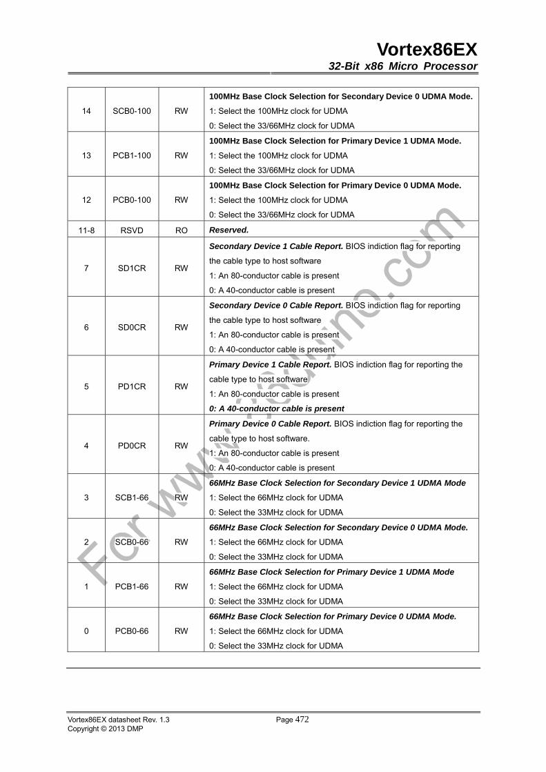
Vortex86EX32-Bit x86 Micro Processor
Vortex86EX datasheet Rev. 1.3 Page 472Copyright © 2013 DMP
14 SCB0-100 RW
100MHz Base Clock Selection for Secondary Device 0 UDMA Mode.
1: Select the 100MHz clock for UDMA
0: Select the 33/66MHz clock for UDMA
13 PCB1-100 RW
100MHz Base Clock Selection for Primary Device 1 UDMA Mode.
1: Select the 100MHz clock for UDMA
0: Select the 33/66MHz clock for UDMA
12 PCB0-100 RW
100MHz Base Clock Selection for Primary Device 0 UDMA Mode.
1: Select the 100MHz clock for UDMA
0: Select the 33/66MHz clock for UDMA
11-8 RSVD RO Reserved.
7 SD1CR RW
Secondary Device 1 Cable Report. BIOS indiction flag for reporting
the cable type to host software
1: An 80-conductor cable is present
0: A 40-conductor cable is present
6 SD0CR RW
Secondary Device 0 Cable Report. BIOS indiction flag for reporting
the cable type to host software
1: An 80-conductor cable is present
0: A 40-conductor cable is present
5 PD1CR RW
Primary Device 1 Cable Report. BIOS indiction flag for reporting the
cable type to host software
1: An 80-conductor cable is present
0: A 40-conductor cable is present
4 PD0CR RW
Primary Device 0 Cable Report. BIOS indiction flag for reporting the
cable type to host software.
1: An 80-conductor cable is present
0: A 40-conductor cable is present
3 SCB1-66 RW
66MHz Base Clock Selection for Secondary Device 1 UDMA Mode
1: Select the 66MHz clock for UDMA
0: Select the 33MHz clock for UDMA
2 SCB0-66 RW
66MHz Base Clock Selection for Secondary Device 0 UDMA Mode.
1: Select the 66MHz clock for UDMA
0: Select the 33MHz clock for UDMA
1 PCB1-66 RW
66MHz Base Clock Selection for Primary Device 1 UDMA Mode
1: Select the 66MHz clock for UDMA
0: Select the 33MHz clock for UDMA
0 PCB0-66 RW
66MHz Base Clock Selection for Primary Device 0 UDMA Mode.
1: Select the 66MHz clock for UDMA
0: Select the 33MHz clock for UDMA
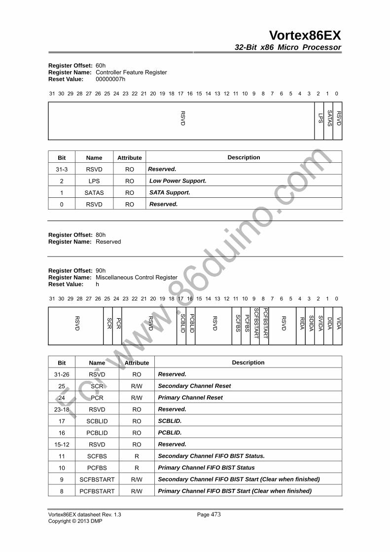
Vortex86EX32-Bit x86 Micro Processor
Vortex86EX datasheet Rev. 1.3 Page 473Copyright © 2013 DMP
Register Offset: 60hRegister Name: Controller Feature Register Reset Value: 00000007h
31 30 29 28 27 26 25 24 23 22 21 20 19 18 17 16 15 14 13 12 11 10 9 8 7 6 5 4 3 2 1 0
Bit Name Attribute Description
31-3 RSVD RO Reserved.
2 LPS RO Low Power Support.
1 SATAS RO SATA Support.
0 RSVD RO Reserved.
Register Offset: 80hRegister Name: Reserved
Register Offset: 90hRegister Name: Miscellaneous Control Register Reset Value: h
31 30 29 28 27 26 25 24 23 22 21 20 19 18 17 16 15 14 13 12 11 10 9 8 7 6 5 4 3 2 1 0
Bit Name Attribute Description
31-26 RSVD RO Reserved.
25 SCR R/W Secondary Channel Reset
24 PCR R/W Primary Channel Reset
23-18 RSVD RO Reserved.
17 SCBLID RO SCBLID.
16 PCBLID RO PCBLID.
15-12 RSVD RO Reserved.
11 SCFBS R Secondary Channel FIFO BIST Status.
10 PCFBS R Primary Channel FIFO BIST Status
9 SCFBSTART R/W Secondary Channel FIFO BIST Start (Clear when finished)
8 PCFBSTART R/W Primary Channel FIFO BIST Start (Clear when finished)
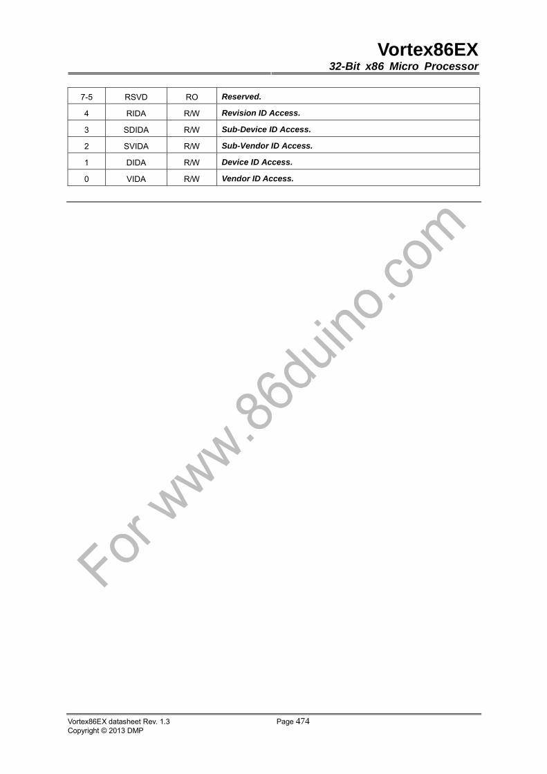
Vortex86EX32-Bit x86 Micro Processor
Vortex86EX datasheet Rev. 1.3 Page 474Copyright © 2013 DMP
7-5 RSVD RO Reserved.
4 RIDA R/W Revision ID Access.
3 SDIDA R/W Sub-Device ID Access.
2 SVIDA R/W Sub-Vendor ID Access.
1 DIDA R/W Device ID Access.
0 VIDA R/W Vendor ID Access.
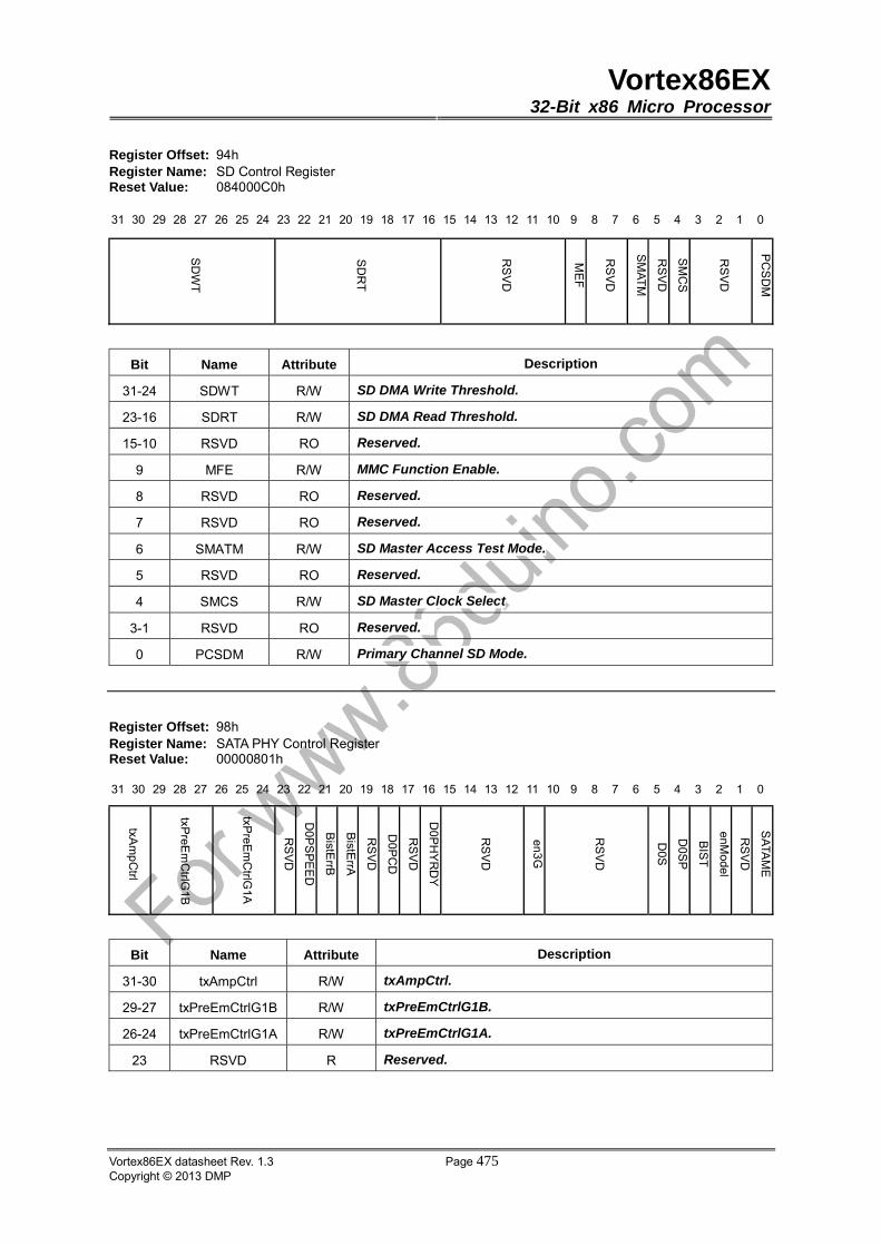
Vortex86EX32-Bit x86 Micro Processor
Vortex86EX datasheet Rev. 1.3 Page 475Copyright © 2013 DMP
Register Offset: 94hRegister Name: SD Control Register Reset Value: 084000C0h
31 30 29 28 27 26 25 24 23 22 21 20 19 18 17 16 15 14 13 12 11 10 9 8 7 6 5 4 3 2 1 0
Bit Name Attribute Description
31-24 SDWT R/W SD DMA Write Threshold.
23-16 SDRT R/W SD DMA Read Threshold.
15-10 RSVD RO Reserved.
9 MFE R/W MMC Function Enable.
8 RSVD RO Reserved.
7 RSVD RO Reserved.
6 SMATM R/W SD Master Access Test Mode.
5 RSVD RO Reserved.
4 SMCS R/W SD Master Clock Select
3-1 RSVD RO Reserved.
0 PCSDM R/W Primary Channel SD Mode.
Register Offset: 98hRegister Name: SATA PHY Control Register Reset Value: 00000801h
31 30 29 28 27 26 25 24 23 22 21 20 19 18 17 16 15 14 13 12 11 10 9 8 7 6 5 4 3 2 1 0
Bit Name Attribute Description
31-30 txAmpCtrl R/W txAmpCtrl.
29-27 txPreEmCtrlG1B R/W txPreEmCtrlG1B.
26-24 txPreEmCtrlG1A R/W txPreEmCtrlG1A.
23 RSVD R Reserved.

Vortex86EX32-Bit x86 Micro Processor
Vortex86EX datasheet Rev. 1.3 Page 476Copyright © 2013 DMP
22 D0PSPEED R
D0 PHY_SPEED.
0:Gen1
1:Gen2
21 BistErrB. R BistErrB.
20 BistErrA. R BistErrA.
19 RSVD R Reserved.
18 D0PCD R D0 PHY COMWAKE Detect
17 RSVD R Reserved.
16 D0PHYRDY R D0 PHYRDY
15-12 RSVD R Reserved.
11 en3G R/W en3G. 0:Only Gen1.
1:Gen1 and Gen2 Enabled
10-8 RSVD R/W Reserved.
7-6 RSVD R Reserved.
5 D0S R/W D0 Slumber (Manual set SATA PHY in slumber mode)
4 D0SP R/W D0 partial (Manual set SATA PHY in partial mode)
3 BIST R/W BIST.
2 enModel R/W enModeI
1 RSVD R/W Reserved.
0 SATAME RO SATA Mode Enable.
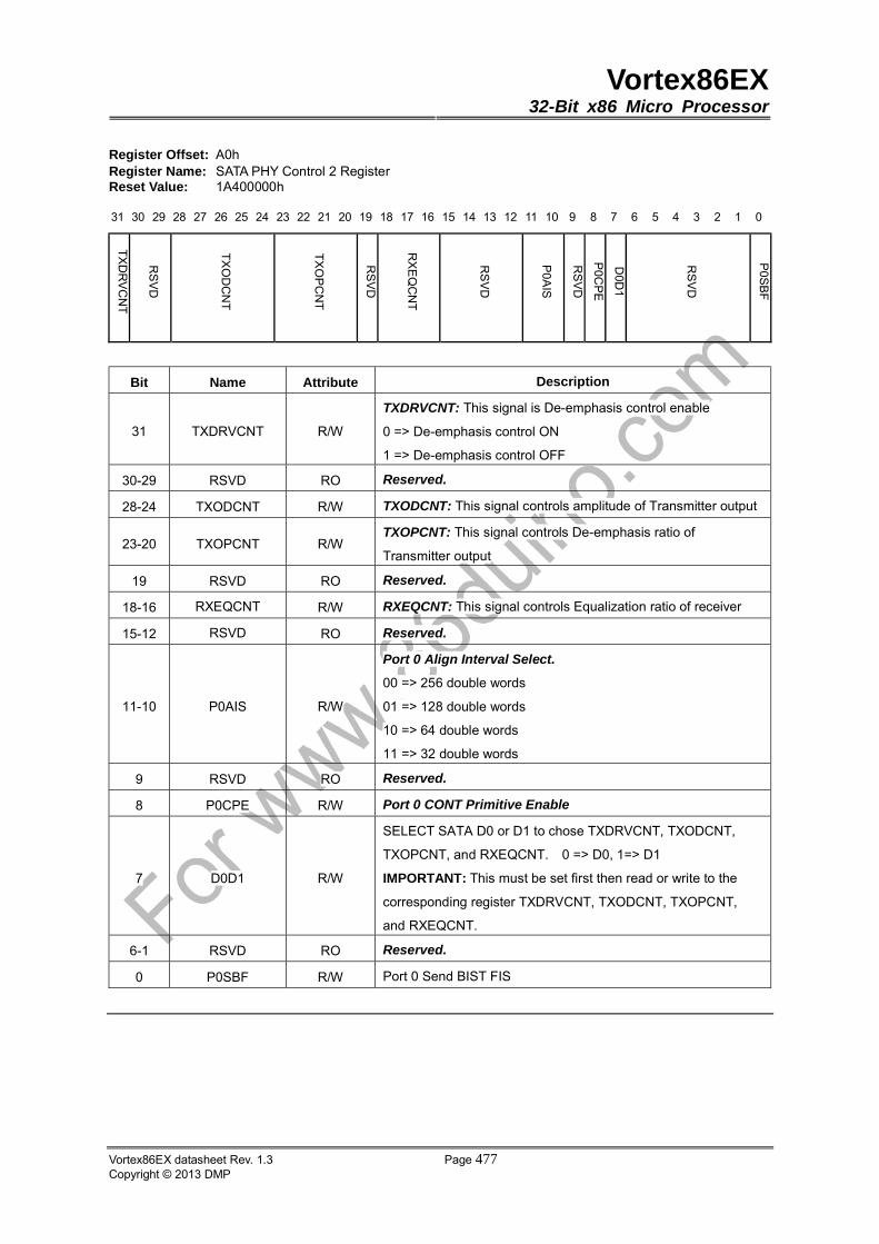
Vortex86EX32-Bit x86 Micro Processor
Vortex86EX datasheet Rev. 1.3 Page 477Copyright © 2013 DMP
Register Offset: A0hRegister Name: SATA PHY Control 2 Register Reset Value: 1A400000h
31 30 29 28 27 26 25 24 23 22 21 20 19 18 17 16 15 14 13 12 11 10 9 8 7 6 5 4 3 2 1 0
Bit Name Attribute Description
31 TXDRVCNT R/W
TXDRVCNT: This signal is De-emphasis control enable
0 => De-emphasis control ON
1 => De-emphasis control OFF
30-29 RSVD RO Reserved.
28-24 TXODCNT R/W TXODCNT: This signal controls amplitude of Transmitter output
23-20 TXOPCNT R/W TXOPCNT: This signal controls De-emphasis ratio of
Transmitter output
19 RSVD RO Reserved.
18-16 RXEQCNT R/W RXEQCNT: This signal controls Equalization ratio of receiver
15-12 RSVD RO Reserved.
11-10 P0AIS R/W
Port 0 Align Interval Select.
00 => 256 double words
01 => 128 double words
10 => 64 double words
11 => 32 double words
9 RSVD RO Reserved.
8 P0CPE R/W Port 0 CONT Primitive Enable
7 D0D1 R/W
SELECT SATA D0 or D1 to chose TXDRVCNT, TXODCNT,
TXOPCNT, and RXEQCNT. 0 => D0, 1=> D1
IMPORTANT: This must be set first then read or write to the
corresponding register TXDRVCNT, TXODCNT, TXOPCNT,
and RXEQCNT.
6-1 RSVD RO Reserved.
0 P0SBF R/W Port 0 Send BIST FIS
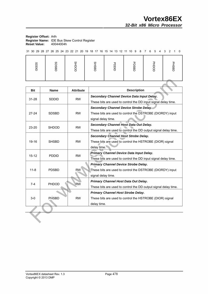
Vortex86EX32-Bit x86 Micro Processor
Vortex86EX datasheet Rev. 1.3 Page 478Copyright © 2013 DMP
Register Offset: A4hRegister Name: IDE Bus Skew Control Register Reset Value: 40044004h
31 30 29 28 27 26 25 24 23 22 21 20 19 18 17 16 15 14 13 12 11 10 9 8 7 6 5 4 3 2 1 0
Bit Name Attribute Description
31-28 SDDID RW Secondary Channel Device Data Input Delay.
These bits are used to control the DD input signal delay time.
27-24 SDSBD RW
Secondary Channel Device Strobe Delay.
These bits are used to control the DSTROBE (DIORDY) input
signal delay time.
23-20 SHDOD RW Secondary Channel Host Data Out Delay.
These bits are used to control the DD output signal delay time.
19-16 SHSBD RW
Secondary Channel Host Strobe Delay.
These bits are used to control the HSTROBE (DIOR) signal
delay time.
15-12 PDDID RW Primary Channel Device Data Input Delay.
These bits are used to control the DD input signal delay time.
11-8 PDSBD RW
Primary Channel Device Strobe Delay.
These bits are used to control the DSTROBE (DIORDY) input
signal delay time.
7-4 PHDOD RW Primary Channel Host Data Out Delay.
These bits are used to control the DD output signal delay time.
3-0 PHSBD RW
Primary Channel Host Strobe Delay.
These bits are used to control the HSTROBE (DIOR) signal
delay time.
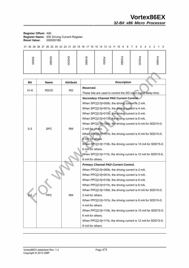
Vortex86EX32-Bit x86 Micro Processor
Vortex86EX datasheet Rev. 1.3 Page 479Copyright © 2013 DMP
Register Offset: A8hRegister Name: IDE Driving Current Register Reset Value: 0000001Bh
31 30 29 28 27 26 25 24 23 22 21 20 19 18 17 16 15 14 13 12 11 10 9 8 7 6 5 4 3 2 1 0
Bit Name Attribute Description
31-6 RSVD RO Reserved.
These bits are used to control the DD input signal delay time.
5-3 SPC RW
Secondary Channel PAD Current Control.
When SPC[2:0]=000b, the driving current is 2 mA.
When SPC[2:0]=001b, the driving current is 4 mA.
When SPC[2:0]=010b, the driving current is 6 mA.
When SPC[2:0]=011b, the driving current is 8 mA,
When SPC[2:0]=100b, the driving current is 6 mA for SDD15-0;
2 mA for others.
When SPC[2:0]=101b, the driving current is 8 mA for SDD15-0;
4 mA for others.
When SPC[2:0]=110b, the driving current is 10 mA for SDD15-0;
6 mA for others.
When SPC[2:0]=111b, the driving current is 12 mA for SDD15-0;
8 mA for others.
2-0 PPC RW
Primary Channel PAD Current Control.
When PPC[2:0]=000b, the driving current is 2 mA.
When PPC[2:0]=001b, the driving current is 4 mA.
When PPC[2:0]=010b, the driving current is 6 mA.
When PPC[2:0]=011b, the driving current is 8 mA,
When PPC[2:0]=100b, the driving current is 6 mA for SDD15-0;
2 mA for others.
When PPC[2:0]=101b, the driving current is 8 mA for SDD15-0;
4 mA for others.
When PPC[2:0]=110b, the driving current is 10 mA for SDD15-0;
6 mA for others.
When PPC[2:0]=111b, the driving current is 12 mA for SDD15-0;
8 mA for others.
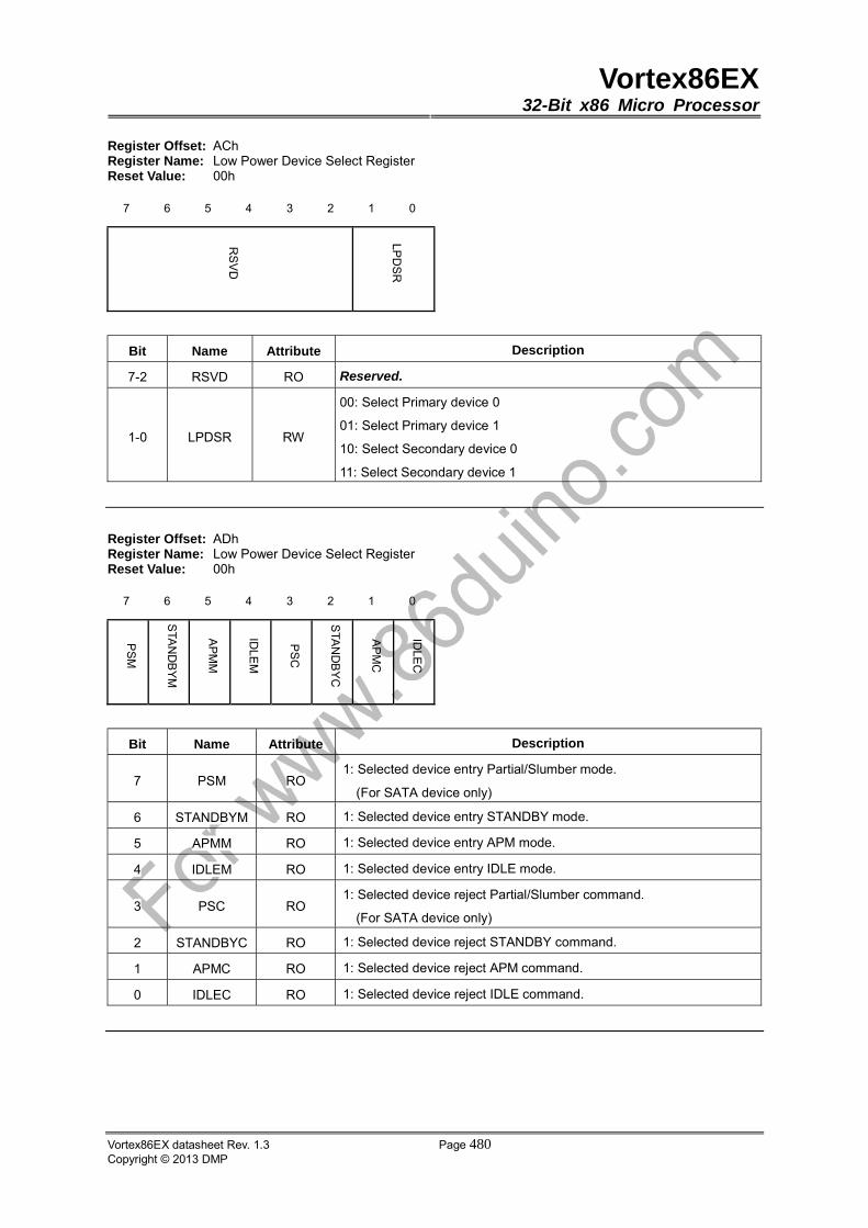
Vortex86EX32-Bit x86 Micro Processor
Vortex86EX datasheet Rev. 1.3 Page 480Copyright © 2013 DMP
Register Offset: ACh Register Name: Low Power Device Select Register Reset Value: 00h
7 6 5 4 3 2 1 0
Bit Name Attribute Description
7-2 RSVD RO Reserved.
1-0 LPDSR RW
00: Select Primary device 0
01: Select Primary device 1
10: Select Secondary device 0
11: Select Secondary device 1
Register Offset: ADh Register Name: Low Power Device Select Register Reset Value: 00h
7 6 5 4 3 2 1 0
Bit Name Attribute Description
7 PSM RO 1: Selected device entry Partial/Slumber mode.
(For SATA device only)
6 STANDBYM RO 1: Selected device entry STANDBY mode.
5 APMM RO 1: Selected device entry APM mode.
4 IDLEM RO 1: Selected device entry IDLE mode.
3 PSC RO 1: Selected device reject Partial/Slumber command.
(For SATA device only)
2 STANDBYC RO 1: Selected device reject STANDBY command.
1 APMC RO 1: Selected device reject APM command.
0 IDLEC RO 1: Selected device reject IDLE command.
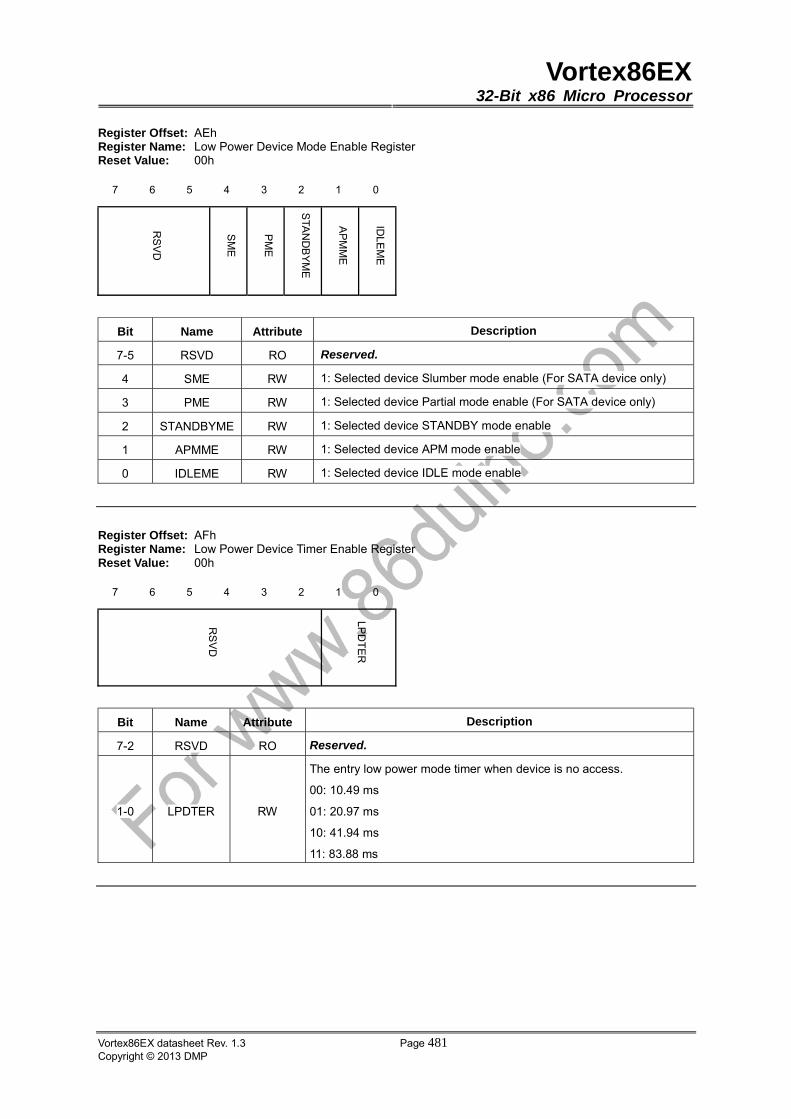
Vortex86EX32-Bit x86 Micro Processor
Vortex86EX datasheet Rev. 1.3 Page 481Copyright © 2013 DMP
Register Offset: AEh Register Name: Low Power Device Mode Enable Register Reset Value: 00h
7 6 5 4 3 2 1 0
Bit Name Attribute Description
7-5 RSVD RO Reserved.
4 SME RW 1: Selected device Slumber mode enable (For SATA device only)
3 PME RW 1: Selected device Partial mode enable (For SATA device only)
2 STANDBYME RW 1: Selected device STANDBY mode enable
1 APMME RW 1: Selected device APM mode enable
0 IDLEME RW 1: Selected device IDLE mode enable
Register Offset: AFh Register Name: Low Power Device Timer Enable Register Reset Value: 00h
7 6 5 4 3 2 1 0
Bit Name Attribute Description
7-2 RSVD RO Reserved.
1-0 LPDTER RW
The entry low power mode timer when device is no access.
00: 10.49 ms
01: 20.97 ms
10: 41.94 ms
11: 83.88 ms

Vortex86EX32-Bit x86 Micro Processor
Vortex86EX datasheet Rev. 1.3 Page 482Copyright © 2013 DMP
13.6 PCI I/O Register -- Bus Master IDE I/O Registers
Register Offset: 00h, 08h Register Name: Primary Bus Master IDE Command Registers, Secondary Bus Master IDE Command
Registers Reset Value: 00h
7 6 5 4 3 2 1 0
RSVD WRC RSVD SBM
Bit Name Attribute Description
7-4 RSVD RO Reserved. These bits must return 0h while being read.
3 WRC RW
Write or Read Control.
This bit sets the direction of the bus master transfer.
1: Bus master writes are performed.
0: Bus master reads are performed.
This bit must not be changed when the bus master function is active.
2-1 RSVD RO Reserved.
0 SBM RW
Start/Stop Bus Master.
Writing a “1” to this bit enables the bus master operation of the
controller. A bus master operation begins when the value of this bit has
changed from a “0” to a “1”. The controller transfers data between the
IDE device and the memory only when this bit is set. Writing a “0” to
this bit can halt the master operation and all the state information is
lost. The master mode operation cannot be stopped and resumed. If
this bit is reset while a bus master operation is still active (BMA=1) and
the drive has not finished its data transfer (INT=0) yet, the bus master
command is aborted, and data transferred from the drive may be
discarded before being written to the system memory. This bit shall be
reset after the data transfer is completed, as indicated by either BMA
being reset or INT being set, or both.
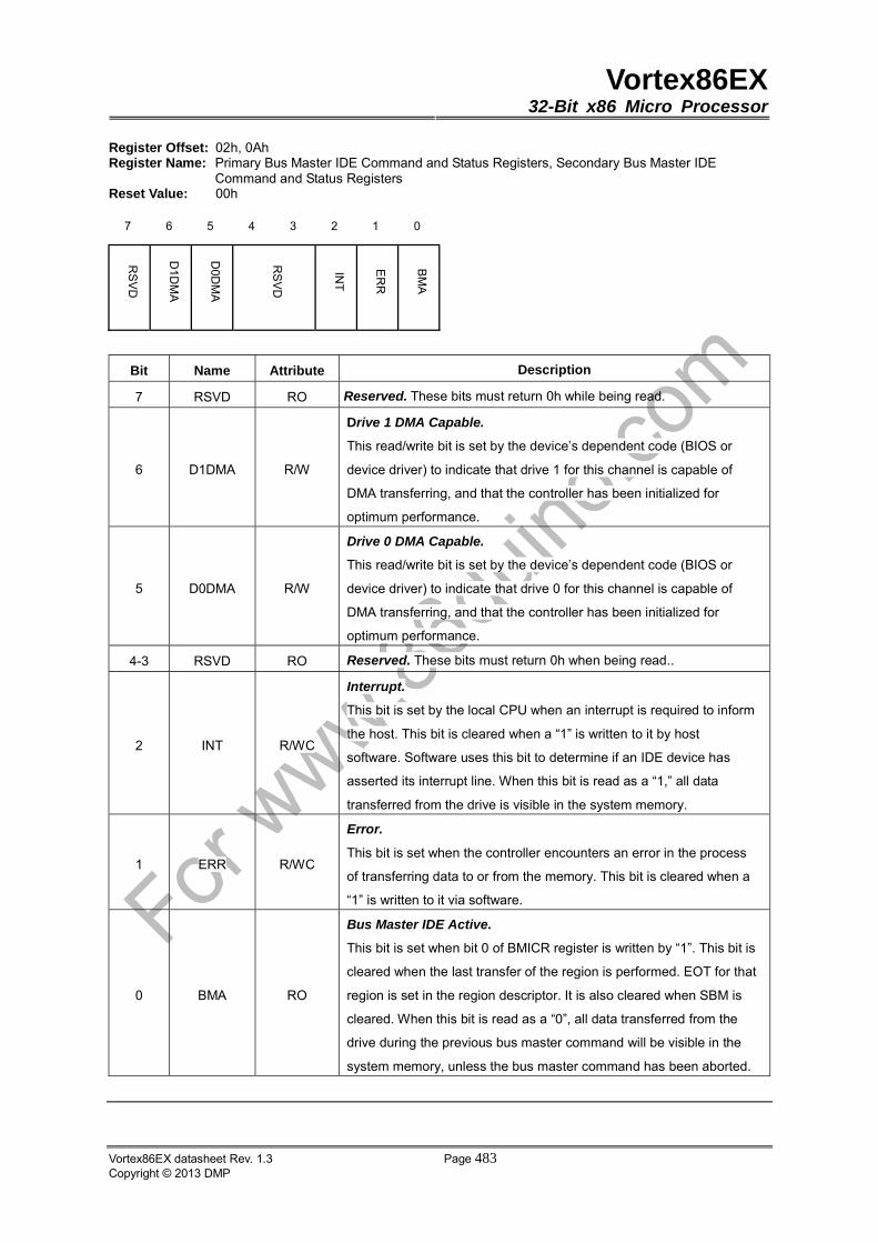
Vortex86EX32-Bit x86 Micro Processor
Vortex86EX datasheet Rev. 1.3 Page 483Copyright © 2013 DMP
Register Offset: 02h, 0Ah Register Name: Primary Bus Master IDE Command and Status Registers, Secondary Bus Master IDE
Command and Status Registers Reset Value: 00h
7 6 5 4 3 2 1 0
Bit Name Attribute Description
7 RSVD RO Reserved. These bits must return 0h while being read.
6 D1DMA R/W
Drive 1 DMA Capable.
This read/write bit is set by the device’s dependent code (BIOS or
device driver) to indicate that drive 1 for this channel is capable of
DMA transferring, and that the controller has been initialized for
optimum performance.
5 D0DMA R/W
Drive 0 DMA Capable.
This read/write bit is set by the device’s dependent code (BIOS or
device driver) to indicate that drive 0 for this channel is capable of
DMA transferring, and that the controller has been initialized for
optimum performance.
4-3 RSVD RO Reserved. These bits must return 0h when being read..
2 INT R/WC
Interrupt.
This bit is set by the local CPU when an interrupt is required to inform
the host. This bit is cleared when a “1” is written to it by host
software. Software uses this bit to determine if an IDE device has
asserted its interrupt line. When this bit is read as a “1,” all data
transferred from the drive is visible in the system memory.
1 ERR R/WC
Error.
This bit is set when the controller encounters an error in the process
of transferring data to or from the memory. This bit is cleared when a
“1” is written to it via software.
0 BMA RO
Bus Master IDE Active.
This bit is set when bit 0 of BMICR register is written by “1”. This bit is
cleared when the last transfer of the region is performed. EOT for that
region is set in the region descriptor. It is also cleared when SBM is
cleared. When this bit is read as a “0”, all data transferred from the
drive during the previous bus master command will be visible in the
system memory, unless the bus master command has been aborted.
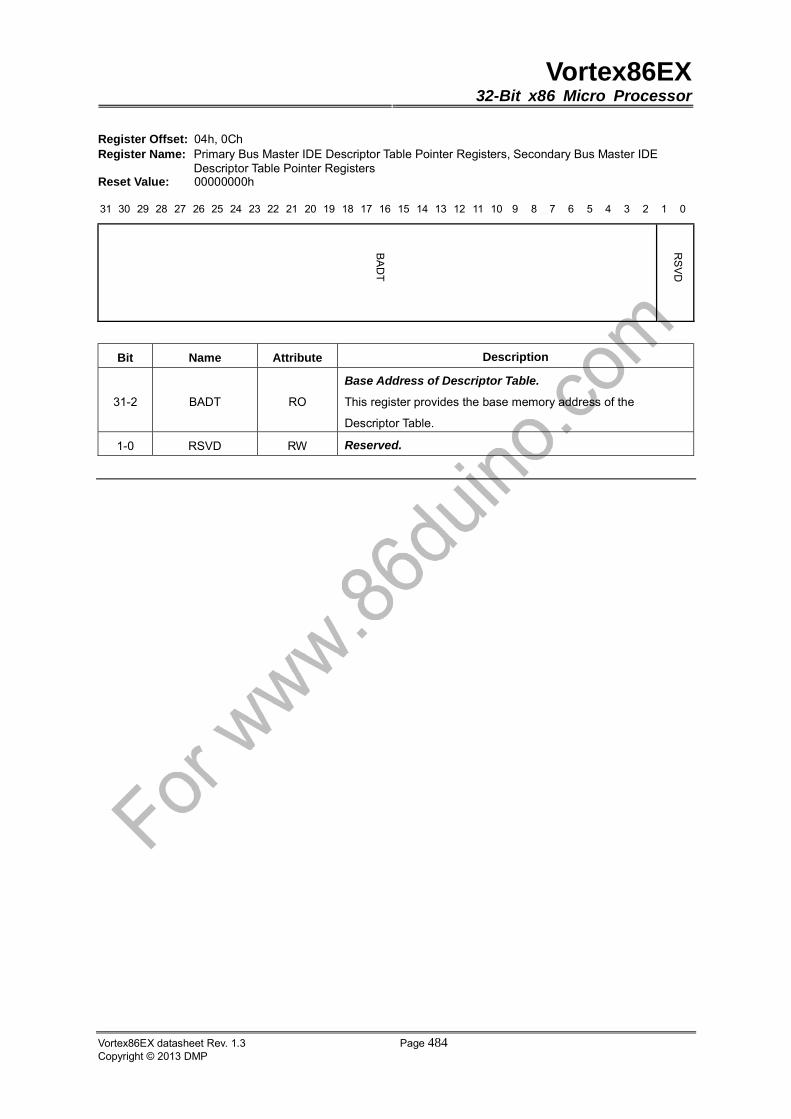
Vortex86EX32-Bit x86 Micro Processor
Vortex86EX datasheet Rev. 1.3 Page 484Copyright © 2013 DMP
Register Offset: 04h, 0Ch Register Name: Primary Bus Master IDE Descriptor Table Pointer Registers, Secondary Bus Master IDE
Descriptor Table Pointer Registers Reset Value: 00000000h
31 30 29 28 27 26 25 24 23 22 21 20 19 18 17 16 15 14 13 12 11 10 9 8 7 6 5 4 3 2 1 0
Bit Name Attribute Description
31-2 BADT RO
Base Address of Descriptor Table.
This register provides the base memory address of the
Descriptor Table.
1-0 RSVD RW Reserved.

Vortex86EX32-Bit x86 Micro Processor
Vortex86EX datasheet Rev. 1.3 Page 485Copyright © 2013 DMP
13.7 IDE Interface and Status Registers
The following registers are used to control the IDE channel action.
The base address of primary IDE Command Registers (offset 0x0 ~0x7) is defined in PCI
Configuration Register 10h~13h (Primary Channel Command Block Register)
The base address of primary IDE Alternate Status/Device Control Register is defined in PCI
Configuration Register 14h~17h (Primary Channel Control Block Register)
The base address of the secondary IDE Command Registers (offset 0x0~0x7) is defined in PCI
Configuration Register 18h~1Bh (Secondary Channel Command Block Register)
The base address of Secondary IDE Alternate Status/Device Control Register is defined in PCI
Configuration Register 1Ch~1Fh (Secondary Channel Control Block Register)
For 13.7.3 ~ 13.7.6 registers, when IDE Device Control Register bit 7 (HOB) is set to 1, these
registers are extended for 48-bit address feature setting for ATA-133 spec. The PCI shares the same
IO space when HOB is 1 or 0. Please refer to the ATA specification for the detailed register
definition.
Register Offset: 00h Register Name: Primary/Secondary IDE Data Registers- PCI IO Space Reset Value: 0000h
15 14 13 12 11 10 9 8 7 6 5 4 3 2 1 0
IDEDR
Bit Name Attribute Description
15-0 IDEDR RW IDE Data Register. This register is for PIO data access only.
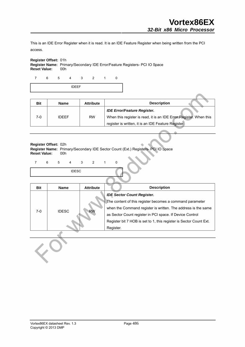
Vortex86EX32-Bit x86 Micro Processor
Vortex86EX datasheet Rev. 1.3 Page 486Copyright © 2013 DMP
This is an IDE Error Register when it is read. It is an IDE Feature Register when being written from the PCI
access.
Register Offset: 01h Register Name: Primary/Secondary IDE Error/Feature Registers- PCI IO Space Reset Value: 00h
7 6 5 4 3 2 1 0
IDEEF
Bit Name Attribute Description
7-0 IDEEF RW
IDE Error/Feature Register.
When this register is read, it is an IDE Error Register. When this
register is written, it is an IDE Feature Register.
Register Offset: 02h Register Name: Primary/Secondary IDE Sector Count (Ext.) Registers- PCI IO Space Reset Value: 00h
7 6 5 4 3 2 1 0
IDESC
Bit Name Attribute Description
7-0 IDESC RW
IDE Sector Count Register.
The content of this register becomes a command parameter
when the Command register is written. The address is the same
as Sector Count register in PCI space. If Device Control
Register bit 7 HOB is set to 1, this register is Sector Count Ext.
Register.
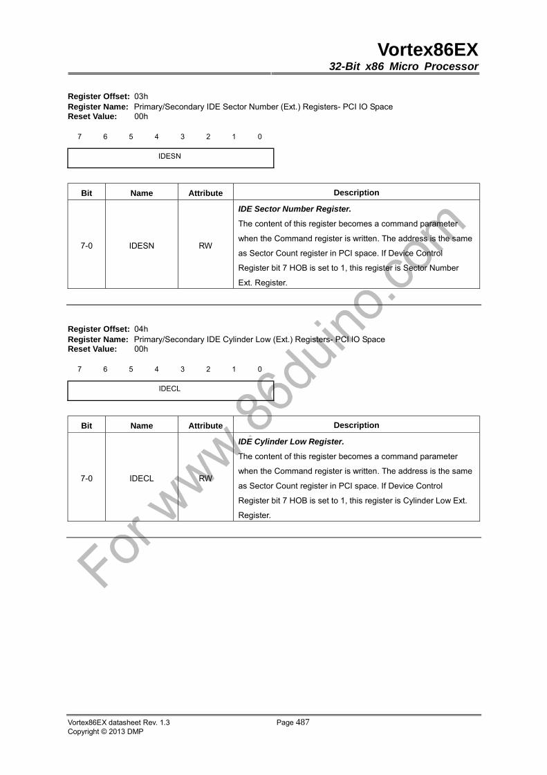
Vortex86EX32-Bit x86 Micro Processor
Vortex86EX datasheet Rev. 1.3 Page 487Copyright © 2013 DMP
Register Offset: 03h Register Name: Primary/Secondary IDE Sector Number (Ext.) Registers- PCI IO Space Reset Value: 00h
7 6 5 4 3 2 1 0
IDESN
Bit Name Attribute Description
7-0 IDESN RW
IDE Sector Number Register.
The content of this register becomes a command parameter
when the Command register is written. The address is the same
as Sector Count register in PCI space. If Device Control
Register bit 7 HOB is set to 1, this register is Sector Number
Ext. Register.
Register Offset: 04h Register Name: Primary/Secondary IDE Cylinder Low (Ext.) Registers- PCI IO Space Reset Value: 00h
7 6 5 4 3 2 1 0
IDECL
Bit Name Attribute Description
7-0 IDECL RW
IDE Cylinder Low Register.
The content of this register becomes a command parameter
when the Command register is written. The address is the same
as Sector Count register in PCI space. If Device Control
Register bit 7 HOB is set to 1, this register is Cylinder Low Ext.
Register.
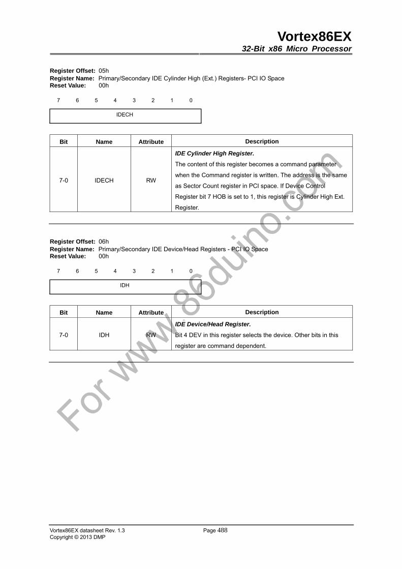
Vortex86EX32-Bit x86 Micro Processor
Vortex86EX datasheet Rev. 1.3 Page 488Copyright © 2013 DMP
Register Offset: 05h Register Name: Primary/Secondary IDE Cylinder High (Ext.) Registers- PCI IO Space Reset Value: 00h
7 6 5 4 3 2 1 0
IDECH
Bit Name Attribute Description
7-0 IDECH RW
IDE Cylinder High Register.
The content of this register becomes a command parameter
when the Command register is written. The address is the same
as Sector Count register in PCI space. If Device Control
Register bit 7 HOB is set to 1, this register is Cylinder High Ext.
Register.
Register Offset: 06h Register Name: Primary/Secondary IDE Device/Head Registers - PCI IO Space Reset Value: 00h
7 6 5 4 3 2 1 0
IDH
Bit Name Attribute Description
7-0 IDH RW
IDE Device/Head Register.
Bit 4 DEV in this register selects the device. Other bits in this
register are command dependent.

Vortex86EX32-Bit x86 Micro Processor
Vortex86EX datasheet Rev. 1.3 Page 489Copyright © 2013 DMP
This is an IDE Status Register when it is read. It is an IDE Command Register when being written
from PCI access.
Register Offset: 07h Register Name: Primary/Secondary IDE Status/Command Registers - PCI IO Space Reset Value: 00h
Status Register
7 6 5 4 3 2 1 0
BUSY DR RSVD DREQ RSVD Error
Bit Name Attribute Description
7 BUSY RO BUSY.
When this bit is set to 1, it indicates that the device is busy.
6 DR RO
Device Ready.
When this bit is set to 1, it indicates that the device is ready and
can accept and attempt to execute all implemented commands.
5-4 RSVD -- Reserved.
3 DREQ RO
Data Request.
When this bit is set to 1, it indicates that the device is ready to
transfer a word of data between the host and device.
2-1 RSVD -- Reserved.
0 Error RO
Error.
When this bit is set to 1, it indicates that an error occurred during
the execution of the previous command.
Command Register
7 6 5 4 3 2 1 0
CC
Bit Name Attribute Description
7-0 CC WO
Command Code.
This register contains the command code being sent to the
device.
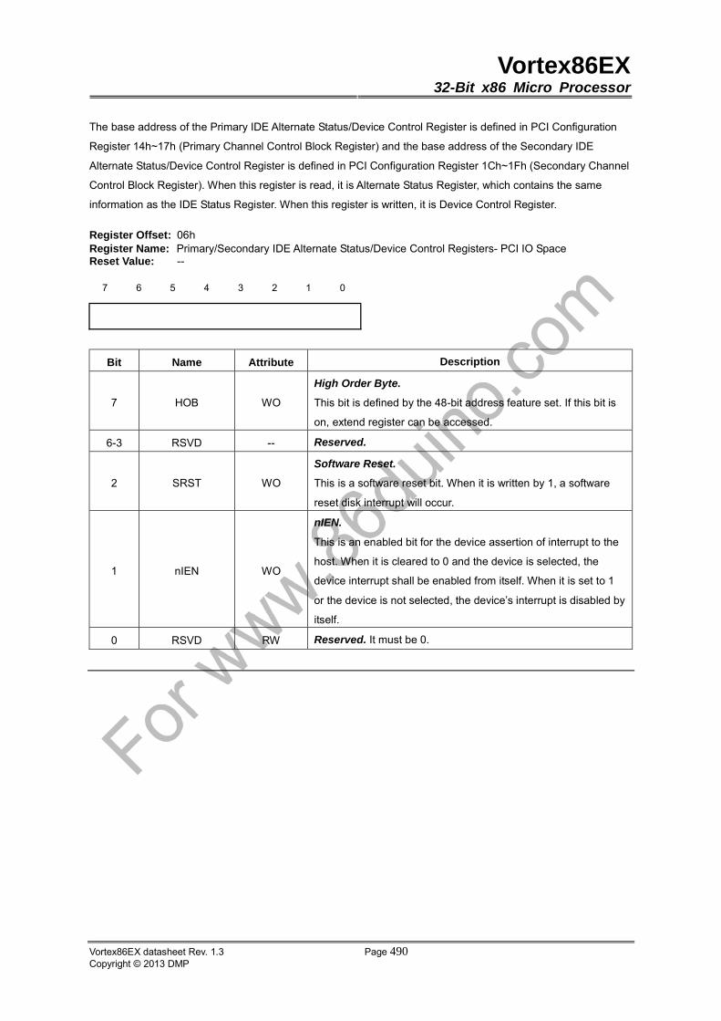
Vortex86EX32-Bit x86 Micro Processor
Vortex86EX datasheet Rev. 1.3 Page 490Copyright © 2013 DMP
The base address of the Primary IDE Alternate Status/Device Control Register is defined in PCI Configuration
Register 14h~17h (Primary Channel Control Block Register) and the base address of the Secondary IDE
Alternate Status/Device Control Register is defined in PCI Configuration Register 1Ch~1Fh (Secondary Channel
Control Block Register). When this register is read, it is Alternate Status Register, which contains the same
information as the IDE Status Register. When this register is written, it is Device Control Register.
Register Offset: 06h Register Name: Primary/Secondary IDE Alternate Status/Device Control Registers- PCI IO Space Reset Value: --
7 6 5 4 3 2 1 0
Bit Name Attribute Description
7 HOB WO
High Order Byte.
This bit is defined by the 48-bit address feature set. If this bit is
on, extend register can be accessed.
6-3 RSVD -- Reserved.
2 SRST WO
Software Reset.
This is a software reset bit. When it is written by 1, a software
reset disk interrupt will occur.
1 nIEN WO
nIEN.
This is an enabled bit for the device assertion of interrupt to the
host. When it is cleared to 0 and the device is selected, the
device interrupt shall be enabled from itself. When it is set to 1
or the device is not selected, the device’s interrupt is disabled by
itself.
0 RSVD RW Reserved. It must be 0.
Vortex86EX32-Bit x86 Micro Processor
Vortex86EX datasheet Rev. 1.3 Page 491Copyright © 2013 DMP
14. Fast Ethernet Control Unit
14.1 Overview
The Fast Ethernat Control unit provides 32-bit performance, PCI bus master capability, and full
compliance with IEEE 802.3u 100Bast-T specifications and IEEE 802.3x Full Duplex Flow
Control.
14.2 Features
� Integrated Fast Ethernet MAC and Physical chip
� 10Mbps and 100Mbps operation
� Supports 10Mbps and 100 Mbps N-way Auto-negotiation operation
� PCI local bus single-chip Fast Ethernet controller
� Provides PCI bus master data transfers
� PCI memory space or I/O space mapped data transfer of operational registers
� Supports digital and analog loopback capability
� Half/Full duplex capability
� Support Full Duplex Flow Control which compliance with IEEE 802.3x
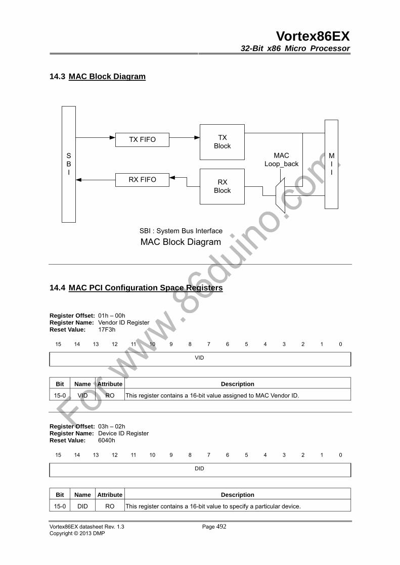
Vortex86EX32-Bit x86 Micro Processor
Vortex86EX datasheet Rev. 1.3 Page 492Copyright © 2013 DMP
14.3 MAC Block Diagram
SBI
TX FIFO
RX FIFO
TXBlock
RXBlock
MII
MACLoop_back
SBI : System Bus Interface
MAC Block Diagram
14.4 MAC PCI Configuration Space Registers
Register Offset: 01h – 00h Register Name: Vendor ID Register Reset Value: 17F3h
15 14 13 12 11 10 9 8 7 6 5 4 3 2 1 0
VID
Bit Name Attribute Description
15-0 VID RO This register contains a 16-bit value assigned to MAC Vendor ID.
Register Offset: 03h – 02h Register Name: Device ID Register Reset Value: 6040h
15 14 13 12 11 10 9 8 7 6 5 4 3 2 1 0
DID
Bit Name Attribute Description
15-0 DID RO This register contains a 16-bit value to specify a particular device.
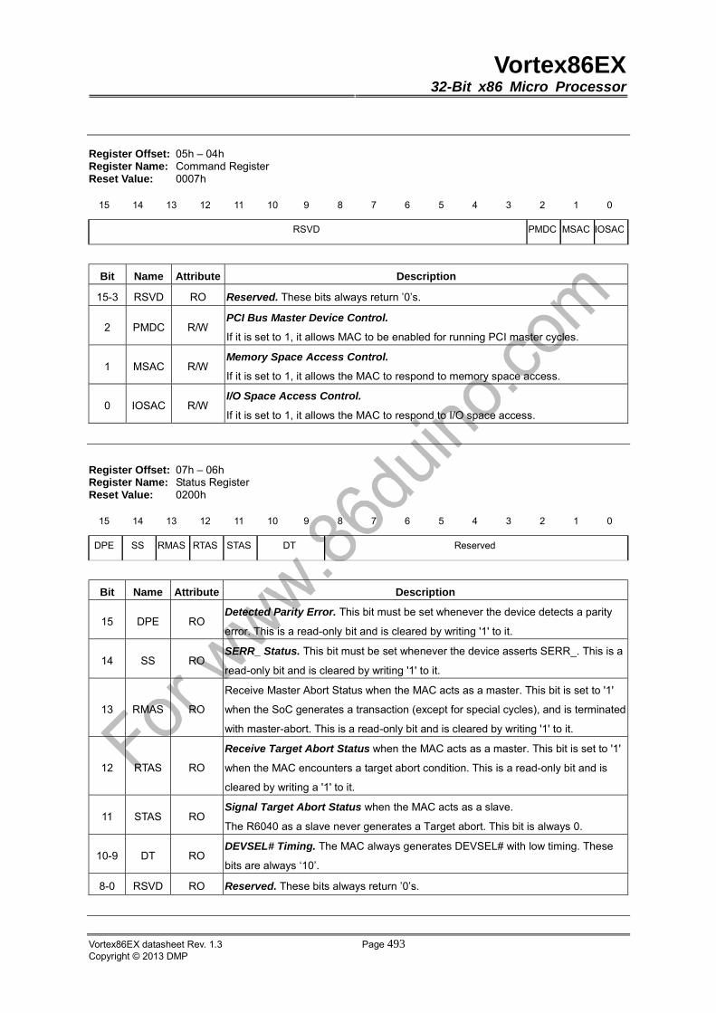
Vortex86EX32-Bit x86 Micro Processor
Vortex86EX datasheet Rev. 1.3 Page 493Copyright © 2013 DMP
Register Offset: 05h – 04h Register Name: Command Register Reset Value: 0007h
15 14 13 12 11 10 9 8 7 6 5 4 3 2 1 0
RSVD PMDC MSAC IOSAC
Bit Name Attribute Description
15-3 RSVD RO Reserved. These bits always return ’0’s.
2 PMDC R/W PCI Bus Master Device Control.
If it is set to 1, it allows MAC to be enabled for running PCI master cycles.
1 MSAC R/W Memory Space Access Control.
If it is set to 1, it allows the MAC to respond to memory space access.
0 IOSAC R/W I/O Space Access Control.
If it is set to 1, it allows the MAC to respond to I/O space access.
Register Offset: 07h – 06h Register Name: Status Register Reset Value: 0200h
15 14 13 12 11 10 9 8 7 6 5 4 3 2 1 0
DPE SS RMAS RTAS STAS DT Reserved
Bit Name Attribute Description
15 DPE RO Detected Parity Error. This bit must be set whenever the device detects a parity
error. This is a read-only bit and is cleared by writing '1' to it.
14 SS RO SERR_ Status. This bit must be set whenever the device asserts SERR_. This is a
read-only bit and is cleared by writing '1' to it.
13 RMAS RO
Receive Master Abort Status when the MAC acts as a master. This bit is set to '1'
when the SoC generates a transaction (except for special cycles), and is terminated
with master-abort. This is a read-only bit and is cleared by writing '1' to it.
12 RTAS RO
Receive Target Abort Status when the MAC acts as a master. This bit is set to '1'
when the MAC encounters a target abort condition. This is a read-only bit and is
cleared by writing a '1' to it.
11 STAS RO Signal Target Abort Status when the MAC acts as a slave.
The R6040 as a slave never generates a Target abort. This bit is always 0.
10-9 DT RO DEVSEL# Timing. The MAC always generates DEVSEL# with low timing. These
bits are always ‘10’.
8-0 RSVD RO Reserved. These bits always return ’0’s.
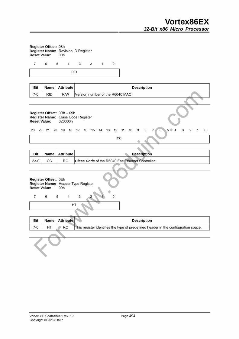
Vortex86EX32-Bit x86 Micro Processor
Vortex86EX datasheet Rev. 1.3 Page 494Copyright © 2013 DMP
Register Offset: 08h Register Name: Revision ID Register Reset Value: 00h
7 6 5 4 3 2 1 0
RID
Bit Name Attribute Description
7-0 RID R/W Version number of the R6040 MAC
Register Offset: 0Bh – 09h Register Name: Class Code Register Reset Value: 020000h
23 22 21 20 19 18 17 16 15 14 13 12 11 10 9 8 7 6 5 4 3 2 1 0
CC
Bit Name Attribute Description
23-0 CC RO Class Code of the R6040 FastEthernet Controller.
Register Offset: 0Eh Register Name: Header Type Register Reset Value: 00h
7 6 5 4 3 2 1 0
HT
Bit Name Attribute Description
7-0 HT RO This register identifies the type of predefined header in the configuration space.
Vortex86EX32-Bit x86 Micro Processor
Vortex86EX datasheet Rev. 1.3 Page 495Copyright © 2013 DMP
15. USB Device Control Unit
15.1 Overview
The USB Device Control unit is an industry-standard USB interface to a simple read/write interface. It
is USB1.1 compliant and supports data transfer at full-speed.
15.2 Features
� Compliant fully with Universal Serial Bus Specification Rev. 1.1
� Supports data transfer at full-speed (12 Mbit/s)
� 3 programmable endpoints and a fixed control IN/OUT endpoint.
� Suspend/resume logic provided

Vortex86EX32-Bit x86 Micro Processor
Vortex86EX datasheet Rev. 1.3 Page 496Copyright © 2013 DMP
15.3 USB Device PCI Configuration Registers Definition
Register Offset: 01h – 00h Register Name: Vendor ID Register Reset Value : 17F3h
15 14 13 12 11 10 9 8 7 6 5 4 3 2 1 0
VID
Bit Name Attribute Description
15-0 VID RO Vendor ID.
Register Offset: 03h – 02h Register Name: Device ID Register Reset Value : 1060h
15 14 13 12 11 10 9 8 7 6 5 4 3 2 1 0
DID
Bit Name Attribute Description
15-0 DID RO Device ID.
Register Offset: 05h – 04h Register Name: Command Register Reset Value : 0000h
15 14 13 12 11 10 9 8 7 6 5 4 3 2 1 0
Bit Name Attribute Description
15-9 RSVD RO Reserved.
8 SDE R/W
SERR_ (Response) Detection Enable bit.
If set to 1, USB device controller asserts SERR_ when it detects an address parity
error. SERR_ is not asserted if this bit is 0.
7 RSVD RO Reserved.
6 PER R/W
Parity Error Response.
This bit controls the device’s response to parity errors. When the bit is set, the
device must take its normal action when a parity error is detected. When the bit is
0, the device sets its Detected Parity Error status bit (bit 15 in the Status register)
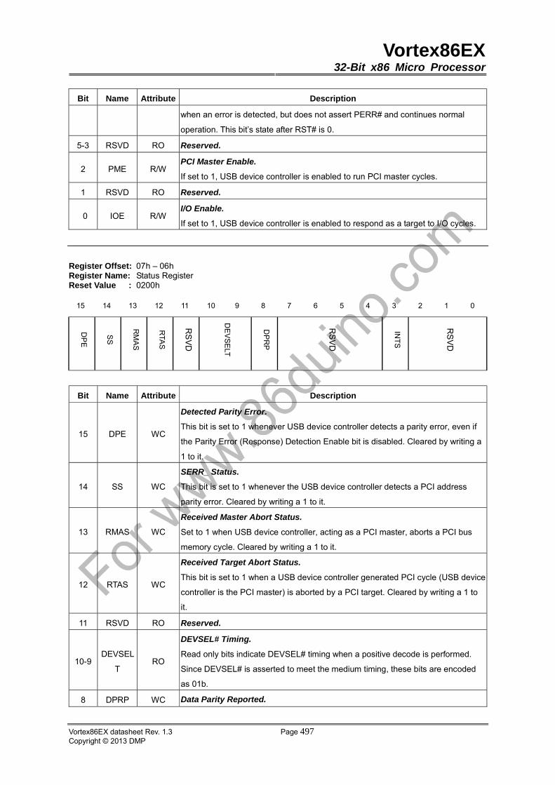
Vortex86EX32-Bit x86 Micro Processor
Vortex86EX datasheet Rev. 1.3 Page 497Copyright © 2013 DMP
Bit Name Attribute Description
when an error is detected, but does not assert PERR# and continues normal
operation. This bit’s state after RST# is 0.
5-3 RSVD RO Reserved.
2 PME R/W PCI Master Enable.
If set to 1, USB device controller is enabled to run PCI master cycles.
1 RSVD RO Reserved.
0 IOE R/W I/O Enable.
If set to 1, USB device controller is enabled to respond as a target to I/O cycles.
Register Offset: 07h – 06h Register Name: Status Register Reset Value : 0200h
15 14 13 12 11 10 9 8 7 6 5 4 3 2 1 0
Bit Name Attribute Description
15 DPE WC
Detected Parity Error.
This bit is set to 1 whenever USB device controller detects a parity error, even if
the Parity Error (Response) Detection Enable bit is disabled. Cleared by writing a
1 to it.
14 SS WC
SERR_ Status.
This bit is set to 1 whenever the USB device controller detects a PCI address
parity error. Cleared by writing a 1 to it.
13 RMAS WC
Received Master Abort Status.
Set to 1 when USB device controller, acting as a PCI master, aborts a PCI bus
memory cycle. Cleared by writing a 1 to it.
12 RTAS WC
Received Target Abort Status.
This bit is set to 1 when a USB device controller generated PCI cycle (USB device
controller is the PCI master) is aborted by a PCI target. Cleared by writing a 1 to
it.
11 RSVD RO Reserved.
10-9DEVSEL
T RO
DEVSEL# Timing.
Read only bits indicate DEVSEL# timing when a positive decode is performed.
Since DEVSEL# is asserted to meet the medium timing, these bits are encoded
as 01b.
8 DPRP WC Data Parity Reported.

Vortex86EX32-Bit x86 Micro Processor
Vortex86EX datasheet Rev. 1.3 Page 498Copyright © 2013 DMP
Bit Name Attribute Description
Set to 1 if the Parity Error Response bit is set, and USB device controller detects
PERR_ asserted while acting as PCI master (whether PERR_ was driven by USB
HC or not).
7-4 RSVD RO Reserved.
3 INTS RO Interrupt Status.
This bit reflects the state of interrupts in the device.
2-0 RSVD RO Reserved.
Register Offset: 08h Register Name: Revision ID Register Reset Value : 02h
7 6 5 4 3 2 1 0
FTRVL
Bit Name Attribute Description
7-0 FTRVL RO Functional Revision Level.
Register Offset: 0Bh – 09h Register Name: Class Code Register Reset Value : 0D0000h
23 22 21 20 19 18 17 16 15 14 13 12 11 10 9 8 7 6 5 4 3 2 1 0
Bit Name Attribute Description
23-16 BCLS RO Base Class.
The Base Class is 0Dh (Reserved).
15-8 SUBCLS RO Sub Class.
The Sub Class is 00h (Reserved).
7-0 PRGIF RO Programming Interface.
The Programming Interface is 00h (Reserved).

Vortex86EX32-Bit x86 Micro Processor
Vortex86EX datasheet Rev. 1.3 Page 499Copyright © 2013 DMP
Register Offset: 0Ch Register Name: Cache Line Size Register Reset Value : 04h
7 6 5 4 3 2 1 0
CCHLSZ
Bit Name Attribute Description
7-0 CCHLSZ RO
Cache Line Size.
This register identifies the system cache line size in units of 32-bit words. USB
device controller will only store the value of 04h in this register.
Register Offset: 0Dh Register Name: Latency Timer Register Reset Value : 00h
7 6 5 4 3 2 1 0
LTCTimer
Bit Name Attribute Description
7-0 LTCTimer R/W
Latency Timer.
This register identifies the value of the latency timer in PCI clocks for PCI bus
master cycles.
Register Offset: 0Eh Register Name: Header Type Register Reset Value : 00h
7 6 5 4 3 2 1 0
HT
Bit Name Attribute Description
7-0 HT RO
Header Type Register.
This register identifies the type of the predefined header in the configuration
space.
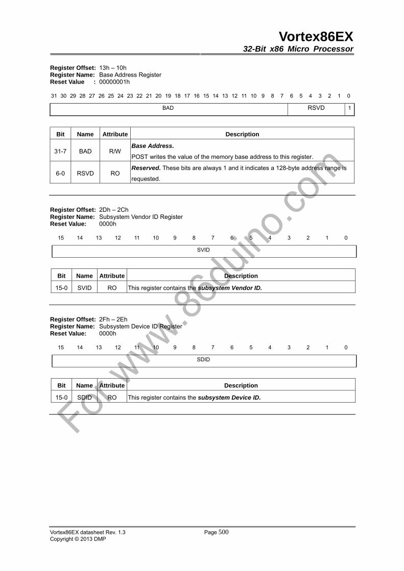
Vortex86EX32-Bit x86 Micro Processor
Vortex86EX datasheet Rev. 1.3 Page 500Copyright © 2013 DMP
Register Offset: 13h – 10h Register Name: Base Address Register Reset Value : 00000001h
31 30 29 28 27 26 25 24 23 22 21 20 19 18 17 16 15 14 13 12 11 10 9 8 7 6 5 4 3 2 1 0
BAD RSVD 1
Bit Name Attribute Description
31-7 BAD R/W Base Address.
POST writes the value of the memory base address to this register.
6-0 RSVD RO Reserved. These bits are always 1 and it indicates a 128-byte address range is
requested.
Register Offset: 2Dh – 2Ch Register Name: Subsystem Vendor ID Register Reset Value: 0000h
15 14 13 12 11 10 9 8 7 6 5 4 3 2 1 0
SVID
Bit Name Attribute Description
15-0 SVID RO This register contains the subsystem Vendor ID.
Register Offset: 2Fh – 2Eh Register Name: Subsystem Device ID Register Reset Value: 0000h
15 14 13 12 11 10 9 8 7 6 5 4 3 2 1 0
SDID
Bit Name Attribute Description
15-0 SDID RO This register contains the subsystem Device ID.

Vortex86EX32-Bit x86 Micro Processor
Vortex86EX datasheet Rev. 1.3 Page 501Copyright © 2013 DMP
Register Offset: 3Dh – 3Ch Register Name: Interrupt Control Register Reset Value: 01FFh
15 14 13 12 11 10 9 8 7 6 5 4 3 2 1 0
INTP INTL
Bit Name Attribute Description
15-8 INTP RO Interrupt Pin. Use INT_A.
7-0 INTL R/W Interrupt Line. Index Interrupt Vector.
Register Offset: 3Eh Register Name: Minimum Grant Register Reset Value : 00h
7 6 5 4 3 2 1 0
MINGNT
Bit Name Attribute Description
7-0 MINGNT RO Minimum Grant.
Register Offset: 3Fh Register Name: Max Latency Register Reset Value : 00h
7 6 5 4 3 2 1 0
MAXLAT
Bit Name Attribute Description
7-0 MAXLAT RO Maximum Latency.

Vortex86EX32-Bit x86 Micro Processor
Vortex86EX datasheet Rev. 1.3 Page 502Copyright © 2013 DMP
15.4 USB Device Operational Registers
The USB device address register holds the device address assigned by the host. This register
initializes to the default address 0 at reset but must be updated by firmware when the host assigns a
new address. Only USB data sent to the address contained in this register will be responded to, all
others are ignored.
Register Offset: 00h Register Name: USB device address register Reset Value: 00h
7 6 5 4 3 2 1 0
DEVE
N DEVADDR[6:0]
Bit Name Attribute Description
7 DEVEN R/W Logic 1 enables the device.
6-0 DEVADDR[6:0] R/W This field specifies the USB device address.
Register Offset: 02h Register Name: Control function register Reset Value: 00h
7 6 5 4 3 2 1 0
RSVD SNDR
SU
SFRES
ET
GLINT
ENA
Bit Name Attribute Description
7-3 RSVD RO Reserved.
2 SNDRSU R/W
Send Resume: Writing logic 1 will generate an upstream resume signal of
1ms duration. This bit is self-clearing after resume completed. Writing logic
0 has no effect. See Figure15-1-Spend/Resume flow.
1 SFRESET R/W
Soft Reset: Writing logic 1 to enable a software-initiated reset to the USB
device controller. BRST interrupt will then not generate any interrupt
request. This bit is self-clearing after reset. Writing logic 0 has no effect. A
soft reset is similar to a hardware-initiated reset (via the RESET_ pin).
0 GLINTENA R/W
Global Interrupt Enable: Logic 1 enables all interrupts. Individual
interrupts can be masked by clearing the corresponding bits in the Interrupt
Enable register.
When this bit is not set, an unmasked interrupt will not generate an interrupt
on the interrupt pin. If global interrupt, however, is enabled while there is
any pending unmasked interrupt, an interrupt signal will be immediately
generated on the interrupt pin.
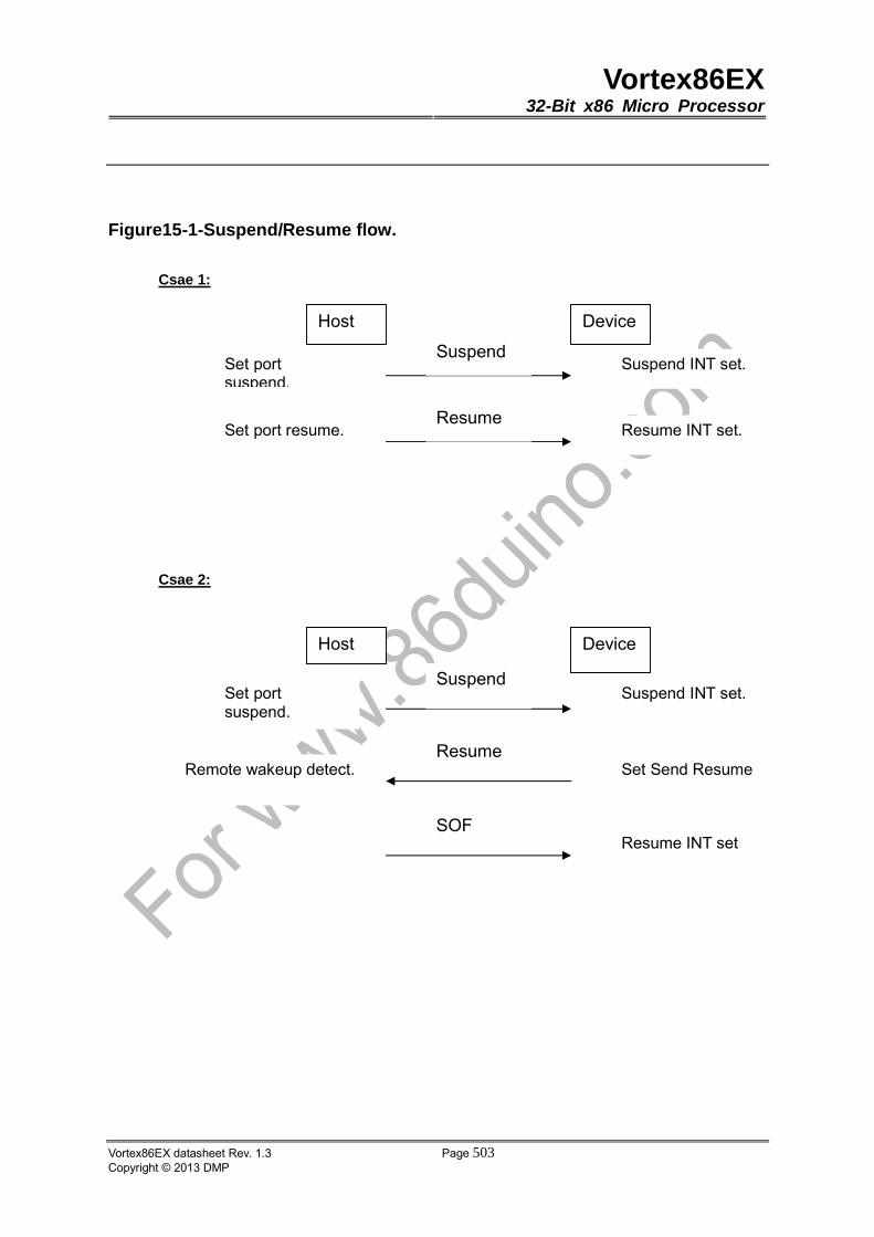
Vortex86EX32-Bit x86 Micro Processor
Vortex86EX datasheet Rev. 1.3 Page 503Copyright © 2013 DMP
Figure15-1-Suspend/Resume flow.
Host Device
Suspend Suspend INT set.
Resume Resume INT set.
Set port suspend.
Set port resume.
Csae 1:
Csae 2:
Host Device
Suspend Suspend INT set.
Resume Set Send Resume
Set port suspend.
Remote wakeup detect.
SOF Resume INT set

Vortex86EX32-Bit x86 Micro Processor
Vortex86EX datasheet Rev. 1.3 Page 504Copyright © 2013 DMP
Register Offset: 07h –06h Register Name: Frame number registerReset Value: 0000h
15 14 13 12 11 10 9 8 7 6 5 4 3 2 1 0
RSVD SOFR[10:0]
Bit Name Attribute Description
15-11 RSVD RO Reserved.
10-0EPMPS[10:
0] RO Frame number.
Register Offset: 0Bh – 08h Register Name: Interrupt enable register Reset Value : 00000000h
31 30 29 28 27 26 25 24 23 22 21 20 19 18 17 16 15 14 13 12 11 10 9 8 7 6 5 4 3 2 1 0
Bit Name Attribute Description
31-17 RSVD RO Reserved.
16 IEP3TX R/W Logic 1 enables interrupt from the indicated endpoint.
15 IEP3RX R/W Logic 1 enables interrupt from the indicated endpoint.
14 IEP2TX R/W Logic 1 enables interrupt from the indicated endpoint.
13 IEP2RX R/W Logic 1 enables interrupt from the indicated endpoint.
12 IEP1TX R/W Logic 1 enables interrupt from the indicated endpoint.
11 IEP1RX R/W Logic 1 enables interrupt from the indicated endpoint.
10 IEP0TX R/W Logic 1 enables interrupt from the control IN endpoint 0.
9 IEP0RX R/W Logic 1 enables interrupt from the control OUT endpoint 0.
8 IEP0SETUP R/W Logic 1 enables interrupt for the setup data received on endpoint 0.
7-5 RSVD RO Reserved.
4 SYSERR R/W
Logic 1 enables interrupt on detection of system error state, like FIFO
Underrun, FIFO Overrun and PCI error include PCI Parity Error, PCI Master
Abort, PCI Target Abort.
3 IERESM R/W Logic 1 enables interrupt on detection of a resume state.
2 IESUSP R/W Logic 1 enables interrupt on detection of a suspend state.
1 IESOF R/W Logic 1 enables interrupt on detection of an SOF.

Vortex86EX32-Bit x86 Micro Processor
Vortex86EX datasheet Rev. 1.3 Page 505Copyright © 2013 DMP
0 IEBRST R/W Logic 1 enables interrupt on detection of a bus reset.
Register Offset: 0Fh – 0Ch Register Name: Interrupt status register Reset Value : 00000000h
31 30 29 28 27 26 25 24 23 22 21 20 19 18 17 16 15 14 13 12 11 10 9 8 7 6 5 4 3 2 1 0
Bit Name Attribute Description
31-17 RSVD RO Reserved.
16 EP3TX W1C Logic 1 indicates the endpoint 3 TX buffer as interrupt source.
15 EP3RX W1C Logic 1 indicates the endpoint 3 RX buffer as interrupt source.
14 EP2TX W1C Logic 1 indicates the endpoint 2 TX buffer as interrupt source.
13 EP2RX W1C Logic 1 indicates the endpoint 2 RX buffer as interrupt source.
12 EP1TX W1C Logic 1 indicates the endpoint 1 TX buffer as interrupt source.
11 EP1RX W1C Logic 1 indicates the endpoint 1 RX buffer as interrupt source.
10 EP0TX W1C Logic 1 indicates the endpoint 0 TX buffer as interrupt source.
9 EP0RX W1C Logic 1 indicates the endpoint 0 RX buffer as interrupt source.
8 EP0SETUP W1C Logic 1 indicates that a SETUP token was received on endpoint 0.
7-5 RSVD RO Reserved.
4 SYSERR W1C
System error: Logic 1 indicates that detection of system error state, like
FIFO Underrun, FIFO Overrun and PCI Error include PCI Parity error, PCI
Master Abort, PCI Target Abort.
3 RESM W1C Resume status: Logic 1 indicates that a status change from suspend to
resume (active) was detected.
2 SUSP W1C Suspend status: Logic 1 indicates that a status change from active to
suspend was detected on the bus.
1 SOF W1C SOF interrupt: Logic 1 indicates that a SOF was received.
0 BRST W1C
Bus reset: Logic 1 indicates that a USB bus reset was detected. When the
device controller detect host drive SE0 state above 1ms and the device
controller will issue the bus reset interrupt after the host exit SE0 state.
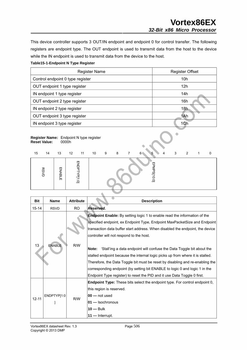
Vortex86EX32-Bit x86 Micro Processor
Vortex86EX datasheet Rev. 1.3 Page 506Copyright © 2013 DMP
This device controller supports 3 OUT/IN endpoint and endpoint 0 for control transfer. The following
registers are endpoint type. The OUT endpoint is used to transmit data from the host to the device
while the IN endpoint is used to transmit data from the device to the host.
Table15-1-Endpoint N Type Register
Register Name Register Offset
Control endpoint 0 type register 10h
OUT endpoint 1 type register 12h
IN endpoint 1 type register 14h
OUT endpoint 2 type register 16h
IN endpoint 2 type register 18h
OUT endpoint 3 type register 1Ah
IN endpoint 3 type register 1Ch
Register Name: Endpoint N type registerReset Value: 0000h
15 14 13 12 11 10 9 8 7 6 5 4 3 2 1 0
Bit Name Attribute Description
15-14 RSVD RO Reserved.
13 ENABLE R/W
Endpoint Enable: By setting logic 1 to enable read the information of the
specified endpoint, ex Endpoint Type, Endpoint MaxPacketSize and Endpoint
transaction data buffer start address. When disabled the endpoint, the device
controller will not respond to the host.
Note: ‘Stall’ing a data endpoint will confuse the Data Toggle bit about the
stalled endpoint because the internal logic picks up from where it is stalled.
Therefore, the Data Toggle bit must be reset by disabling and re-enabling the
corresponding endpoint (by setting bit ENABLE to logic 0 and logic 1 in the
Endpoint Type register) to reset the PID and it use Data Toggle 0 first.
12-11ENDPTYP[1:0
] R/W
Endpoint Type: These bits select the endpoint type. For control endpoint 0,
this region is reserved.
00 — not used
01 — Isochronous
10 — Bulk
11 — Interrupt.
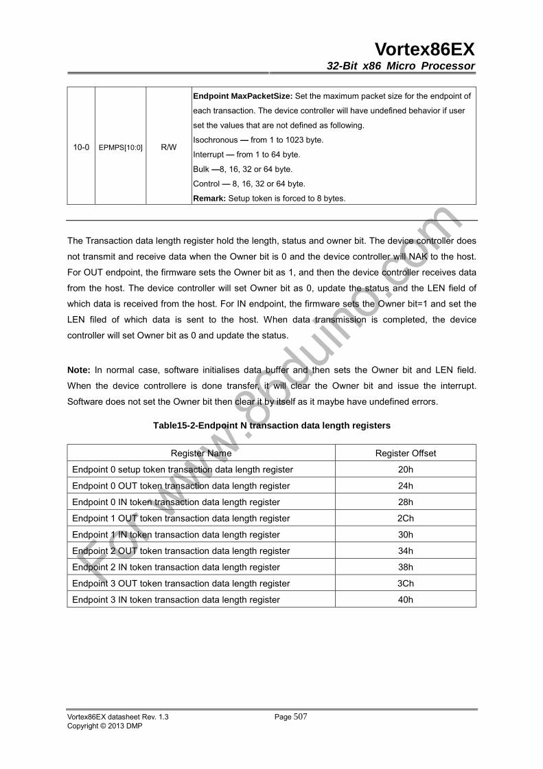
Vortex86EX32-Bit x86 Micro Processor
Vortex86EX datasheet Rev. 1.3 Page 507Copyright © 2013 DMP
10-0 EPMPS[10:0] R/W
Endpoint MaxPacketSize: Set the maximum packet size for the endpoint of
each transaction. The device controller will have undefined behavior if user
set the values that are not defined as following.
Isochronous — from 1 to 1023 byte.
Interrupt — from 1 to 64 byte.
Bulk —8, 16, 32 or 64 byte.
Control — 8, 16, 32 or 64 byte.
Remark: Setup token is forced to 8 bytes.
The Transaction data length register hold the length, status and owner bit. The device controller does
not transmit and receive data when the Owner bit is 0 and the device controller will NAK to the host.
For OUT endpoint, the firmware sets the Owner bit as 1, and then the device controller receives data
from the host. The device controller will set Owner bit as 0, update the status and the LEN field of
which data is received from the host. For IN endpoint, the firmware sets the Owner bit=1 and set the
LEN filed of which data is sent to the host. When data transmission is completed, the device
controller will set Owner bit as 0 and update the status.
Note: In normal case, software initialises data buffer and then sets the Owner bit and LEN field.
When the device controllere is done transfer, it will clear the Owner bit and issue the interrupt.
Software does not set the Owner bit then clear it by itself as it maybe have undefined errors.
Table15-2-Endpoint N transaction data length registers
Register Name Register Offset
Endpoint 0 setup token transaction data length register 20h
Endpoint 0 OUT token transaction data length register 24h
Endpoint 0 IN token transaction data length register 28h
Endpoint 1 OUT token transaction data length register 2Ch
Endpoint 1 IN token transaction data length register 30h
Endpoint 2 OUT token transaction data length register 34h
Endpoint 2 IN token transaction data length register 38h
Endpoint 3 OUT token transaction data length register 3Ch
Endpoint 3 IN token transaction data length register 40h
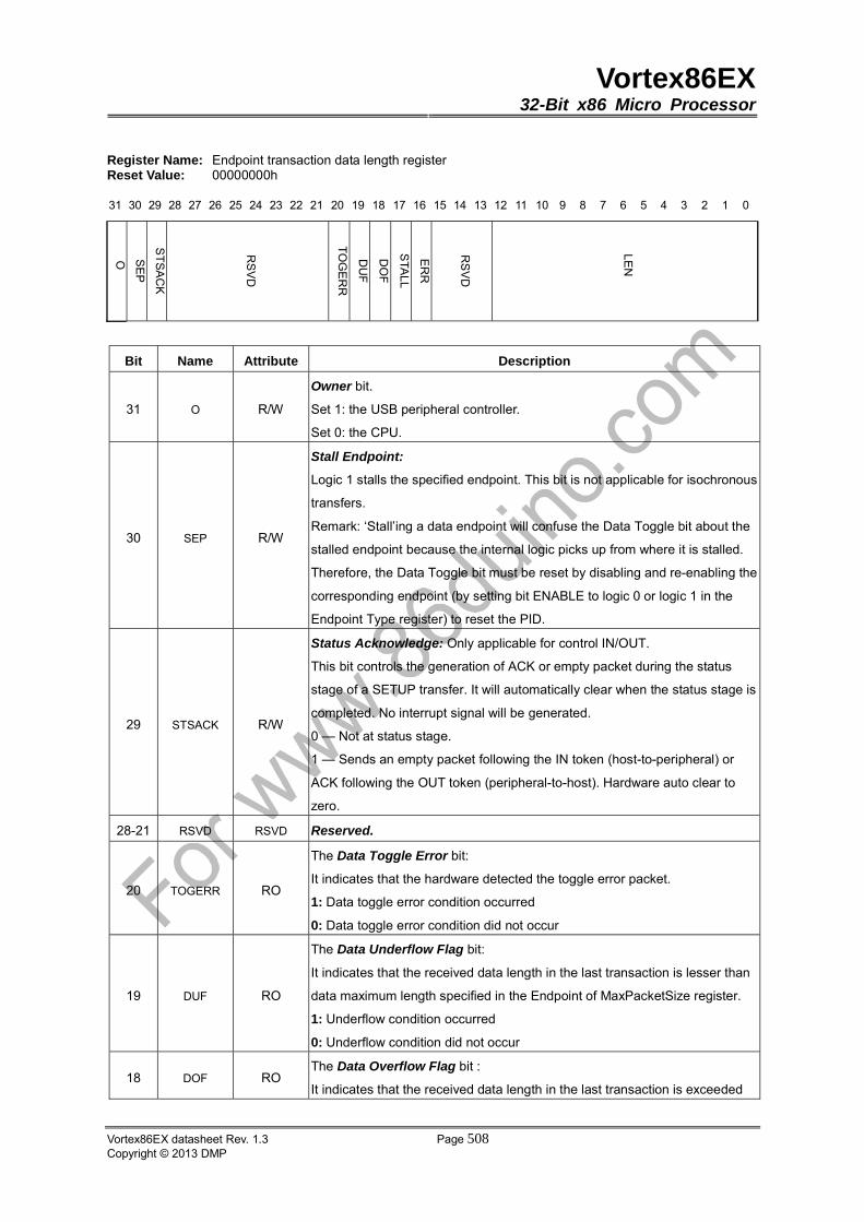
Vortex86EX32-Bit x86 Micro Processor
Vortex86EX datasheet Rev. 1.3 Page 508Copyright © 2013 DMP
Register Name: Endpoint transaction data length register Reset Value: 00000000h
31 30 29 28 27 26 25 24 23 22 21 20 19 18 17 16 15 14 13 12 11 10 9 8 7 6 5 4 3 2 1 0
Bit Name Attribute Description
31 O R/W
Owner bit.
Set 1: the USB peripheral controller.
Set 0: the CPU.
30 SEP R/W
Stall Endpoint:
Logic 1 stalls the specified endpoint. This bit is not applicable for isochronous
transfers.
Remark: ‘Stall’ing a data endpoint will confuse the Data Toggle bit about the
stalled endpoint because the internal logic picks up from where it is stalled.
Therefore, the Data Toggle bit must be reset by disabling and re-enabling the
corresponding endpoint (by setting bit ENABLE to logic 0 or logic 1 in the
Endpoint Type register) to reset the PID.
29 STSACK R/W
Status Acknowledge: Only applicable for control IN/OUT.
This bit controls the generation of ACK or empty packet during the status
stage of a SETUP transfer. It will automatically clear when the status stage is
completed. No interrupt signal will be generated.
0 — Not at status stage.
1 — Sends an empty packet following the IN token (host-to-peripheral) or
ACK following the OUT token (peripheral-to-host). Hardware auto clear to
zero.
28-21 RSVD RSVD Reserved.
20 TOGERR RO
The Data Toggle Error bit:
It indicates that the hardware detected the toggle error packet.
1: Data toggle error condition occurred
0: Data toggle error condition did not occur
19 DUF RO
The Data Underflow Flag bit:
It indicates that the received data length in the last transaction is lesser than
data maximum length specified in the Endpoint of MaxPacketSize register.
1: Underflow condition occurred
0: Underflow condition did not occur
18 DOF ROThe Data Overflow Flag bit :
It indicates that the received data length in the last transaction is exceeded
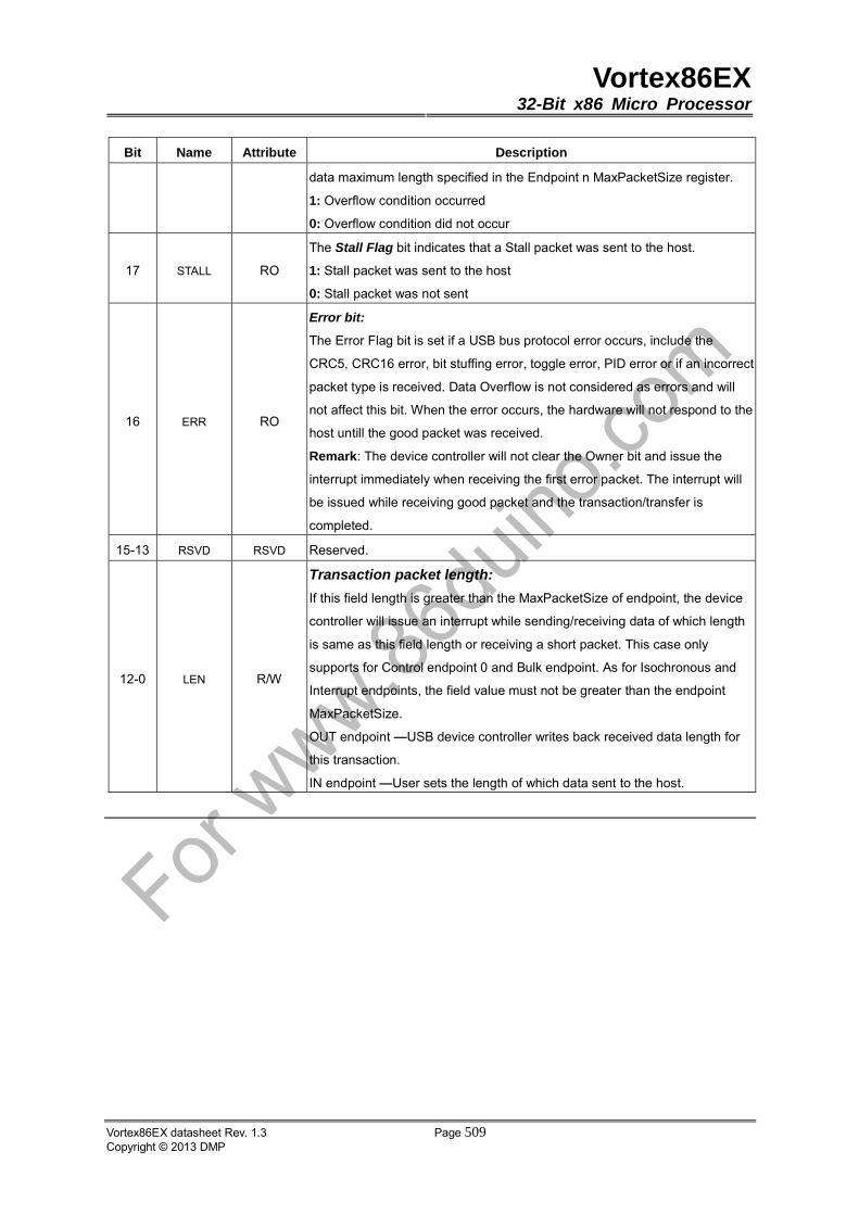
Vortex86EX32-Bit x86 Micro Processor
Vortex86EX datasheet Rev. 1.3 Page 509Copyright © 2013 DMP
Bit Name Attribute Description
data maximum length specified in the Endpoint n MaxPacketSize register.
1: Overflow condition occurred
0: Overflow condition did not occur
17 STALL RO
The Stall Flag bit indicates that a Stall packet was sent to the host.
1: Stall packet was sent to the host
0: Stall packet was not sent
16 ERR RO
Error bit:
The Error Flag bit is set if a USB bus protocol error occurs, include the
CRC5, CRC16 error, bit stuffing error, toggle error, PID error or if an incorrect
packet type is received. Data Overflow is not considered as errors and will
not affect this bit. When the error occurs, the hardware will not respond to the
host untill the good packet was received.
Remark: The device controller will not clear the Owner bit and issue the
interrupt immediately when receiving the first error packet. The interrupt will
be issued while receiving good packet and the transaction/transfer is
completed.
15-13 RSVD RSVD Reserved.
12-0 LEN R/W
Transaction packet length:
If this field length is greater than the MaxPacketSize of endpoint, the device
controller will issue an interrupt while sending/receiving data of which length
is same as this field length or receiving a short packet. This case only
supports for Control endpoint 0 and Bulk endpoint. As for Isochronous and
Interrupt endpoints, the field value must not be greater than the endpoint
MaxPacketSize.
OUT endpoint —USB device controller writes back received data length for
this transaction.
IN endpoint —User sets the length of which data sent to the host.
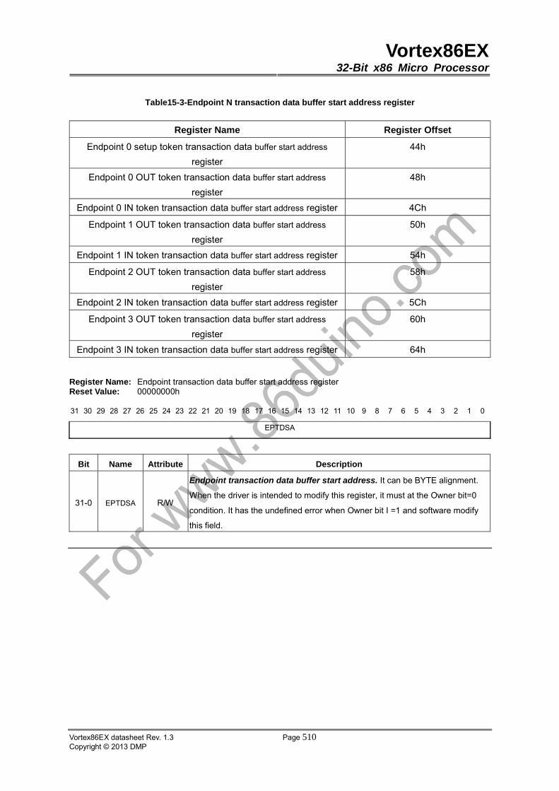
Vortex86EX32-Bit x86 Micro Processor
Vortex86EX datasheet Rev. 1.3 Page 510Copyright © 2013 DMP
Table15-3-Endpoint N transaction data buffer start address register
Register Name Register Offset
Endpoint 0 setup token transaction data buffer start address
register
44h
Endpoint 0 OUT token transaction data buffer start address
register
48h
Endpoint 0 IN token transaction data buffer start address register 4Ch
Endpoint 1 OUT token transaction data buffer start address
register
50h
Endpoint 1 IN token transaction data buffer start address register 54h
Endpoint 2 OUT token transaction data buffer start address
register
58h
Endpoint 2 IN token transaction data buffer start address register 5Ch
Endpoint 3 OUT token transaction data buffer start address
register
60h
Endpoint 3 IN token transaction data buffer start address register 64h
Register Name: Endpoint transaction data buffer start address registerReset Value: 00000000h
31 30 29 28 27 26 25 24 23 22 21 20 19 18 17 16 15 14 13 12 11 10 9 8 7 6 5 4 3 2 1 0
EPTDSA
Bit Name Attribute Description
31-0 EPTDSA R/W
Endpoint transaction data buffer start address. It can be BYTE alignment.
When the driver is intended to modify this register, it must at the Owner bit=0
condition. It has the undefined error when Owner bit I =1 and software modify
this field.
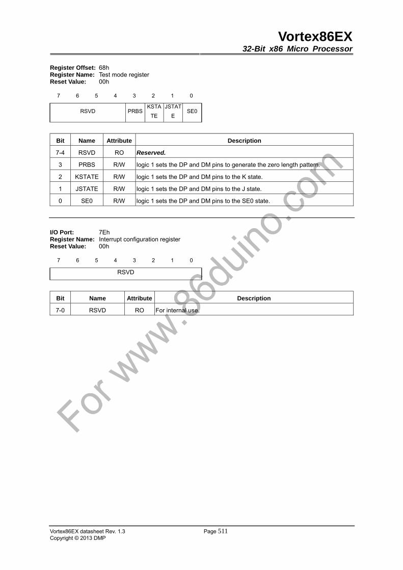
Vortex86EX32-Bit x86 Micro Processor
Vortex86EX datasheet Rev. 1.3 Page 511Copyright © 2013 DMP
Register Offset: 68h Register Name: Test mode registerReset Value: 00h
7 6 5 4 3 2 1 0
RSVD PRBSKSTA
TE
JSTAT
E SE0
Bit Name Attribute Description
7-4 RSVD RO Reserved.
3 PRBS R/W logic 1 sets the DP and DM pins to generate the zero length pattern.
2 KSTATE R/W logic 1 sets the DP and DM pins to the K state.
1 JSTATE R/W logic 1 sets the DP and DM pins to the J state.
0 SE0 R/W logic 1 sets the DP and DM pins to the SE0 state.
I/O Port: 7Eh Register Name: Interrupt configuration register Reset Value: 00h
7 6 5 4 3 2 1 0
RSVD
Bit Name Attribute Description
7-0 RSVD RO For internal use.
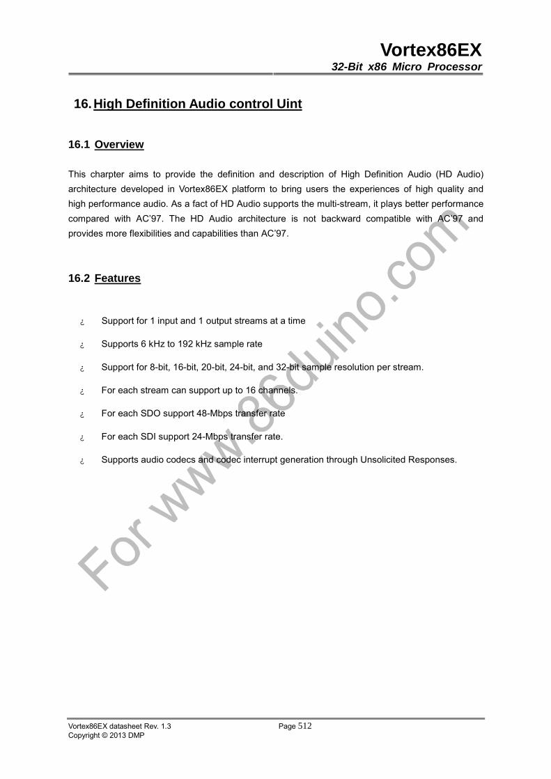
Vortex86EX32-Bit x86 Micro Processor
Vortex86EX datasheet Rev. 1.3 Page 512Copyright © 2013 DMP
16. High Definition Audio control Uint
16.1 Overview
This charpter aims to provide the definition and description of High Definition Audio (HD Audio)
architecture developed in Vortex86EX platform to bring users the experiences of high quality and
high performance audio. As a fact of HD Audio supports the multi-stream, it plays better performance
compared with AC’97. The HD Audio architecture is not backward compatible with AC’97 and
provides more flexibilities and capabilities than AC’97.
16.2 Features
� Support for 1 input and 1 output streams at a time
� Supports 6 kHz to 192 kHz sample rate
� Support for 8-bit, 16-bit, 20-bit, 24-bit, and 32-bit sample resolution per stream.
� For each stream can support up to 16 channels.
� For each SDO support 48-Mbps transfer rate
� For each SDI support 24-Mbps transfer rate.
� Supports audio codecs and codec interrupt generation through Unsolicited Responses.
Vortex86EX32-Bit x86 Micro Processor
Vortex86EX datasheet Rev. 1.3 Page 513Copyright © 2013 DMP
16.3 HDA PCI Configuration Space Registers
Register Offset: 01h – 00h Register Name: Vendor ID Register Reset Value : 17F3h
15 14 13 12 11 10 9 8 7 6 5 4 3 2 1 0
VID
Bit Name Attribute Description
15-0 VID RO Vendor ID.
Register Offset: 03h – 02h Register Name: Device ID Register Reset Value : 3010h
15 14 13 12 11 10 9 8 7 6 5 4 3 2 1 0
DID
Bit Name Attribute Description
15-0 DID RO Device ID.
Register Offset: 05h – 04h Register Name: Command Register Reset Value : 0000h
15 14 13 12 11 10 9 8 7 6 5 4 3 2 1 0
RSVD SDE RSVD PER RSVD PME RSVD IOE
Bit Name Attribute Description
15-9 RSVD RO Reserved.
8 SDE R/W
SERR# (Response) Detection Enable bit.
If set to 1, HDA controller asserts SERR# when it detects an address parity error.
SERR# is not asserted if this bit is 0.
7 RSVD RO Reserved.
6 PER R/W
Parity Error Response.
This bit controls the device's response to parity errors. When the bit is set, the
device must take its normal action when a parity error is detected. When the bit is
0, the device sets its Detected Parity Error status bit (bit 15 in the Status register)
when an error is detected, but does not assert PERR# and continues normal
operation. This bit's state after RST# is 0.

Vortex86EX32-Bit x86 Micro Processor
Vortex86EX datasheet Rev. 1.3 Page 514Copyright © 2013 DMP
5-3 RSVD RO Reserved.
2 PME R/W PCI Master Enable.
If set to 1, HDA controller is enabled to run PCI master cycles.
1 ME R/W Memory Enable.
If set to 1, HDA controller is enabled to respond as a target to memory cycles.
0 RSVD RO Reserved.
Register Offset: 07h – 06h Register Name: Status Register Reset Value : 0200h
15 14 13 12 11 10 9 8 7 6 5 4 3 2 1 0
DPE SS RMAS RTAS RSVD DEVSELT DPRP RSVD INTS RSVD
Bit Name Attribute Description
15 DPE WC
Detected Parity Error.
This bit is set to 1 whenever HDA controller detects a parity error, even if the
Parity Error (Response) Detection Enable bit is disabled. Cleared by writing a 1 to
it.
14 SS WC
SERR# Status.
This bit is set to 1 whenever the HDA controller detects a PCI address parity
error. Cleared by writing a 1 to it.
13 RMAS WC
Received Master Abort Status.
Set to 1 when HDA controller, acting as a PCI master, aborts a PCI bus memory
cycle. Cleared by writing a 1 to it.
12 RTAS WC
Received Target Abort Status.
This bit is set to 1 when a HDA controller generated PCI cycle (HDA controller is
the PCI master) is aborted by a PCI target. Cleared by writing a 1 to it.
11 RSVD RO Reserved.
10-9DEVSEL
T RO
DEVSEL# Timing.
Read only bits indicating DEVSEL# timing when a positive decode is performed.
Since DEVSEL# is asserted to meet the medium timing, these bits are encoded
as 01b.
8 DPRP WC
Data Parity Reported.
Set to 1 if the Parity Error Response bit is set, and HDA controller detects PERR#
asserted while acting as PCI master (whether PERR# was driven by HDA or not).
7-4 RSVD RO Reserved.
3 INTS RO Interrupt Status.
This bit reflects the state of interrupts in the device.
2-0 RSVD RO Reserved.
Vortex86EX32-Bit x86 Micro Processor
Vortex86EX datasheet Rev. 1.3 Page 515Copyright © 2013 DMP
Register Offset: 08h Register Name: Revision ID Register Reset Value : 02h
7 6 5 4 3 2 1 0
FTRVL
Bit Name Attribute Description
7-0 FTRVL RO Functional Revision Level.
Register Offset: 0Bh – 09h Register Name: Class Code Register Reset Value : 040300h
23 22 21 20 19 18 17 16 15 14 13 12 11 10 9 8 7 6 5 4 3 2 1 0
BCLS SUBCLS PRGIF
Bit Name Attribute Description
23-16 BCLS RO Base Class.
The Base Class is 04h.
15-8 SUBCLS RO Sub Class.
The Sub Class is 03h.
7-0 PRGIF RO Programming Interface.
The Programming Interface is 00h.
Register Offset: 0Ch Register Name: Cache Line Size Register Reset Value : 08h
7 6 5 4 3 2 1 0
CCHLSZ
Bit Name Attribute Description
7-0 CCHLSZ RO
Cache Line Size.
This register identifies the system cache line size in units of 32-bit words. HDA
controller will only store the value of 04h in this register.
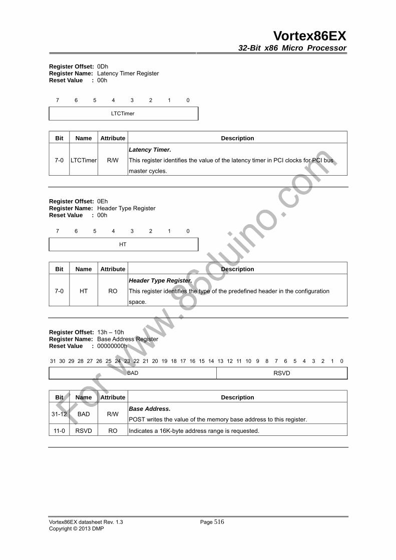
Vortex86EX32-Bit x86 Micro Processor
Vortex86EX datasheet Rev. 1.3 Page 516Copyright © 2013 DMP
Register Offset: 0Dh Register Name: Latency Timer Register Reset Value : 00h
7 6 5 4 3 2 1 0
LTCTimer
Bit Name Attribute Description
7-0 LTCTimer R/W
Latency Timer.
This register identifies the value of the latency timer in PCI clocks for PCI bus
master cycles.
Register Offset: 0Eh Register Name: Header Type Register Reset Value : 00h
7 6 5 4 3 2 1 0
HT
Bit Name Attribute Description
7-0 HT RO
Header Type Register.
This register identifies the type of the predefined header in the configuration
space.
Register Offset: 13h – 10h Register Name: Base Address Register Reset Value : 00000000h
31 30 29 28 27 26 25 24 23 22 21 20 19 18 17 16 15 14 13 12 11 10 9 8 7 6 5 4 3 2 1 0
BAD RSVD
Bit Name Attribute Description
31-12 BAD R/W Base Address.
POST writes the value of the memory base address to this register.
11-0 RSVD RO Indicates a 16K-byte address range is requested.
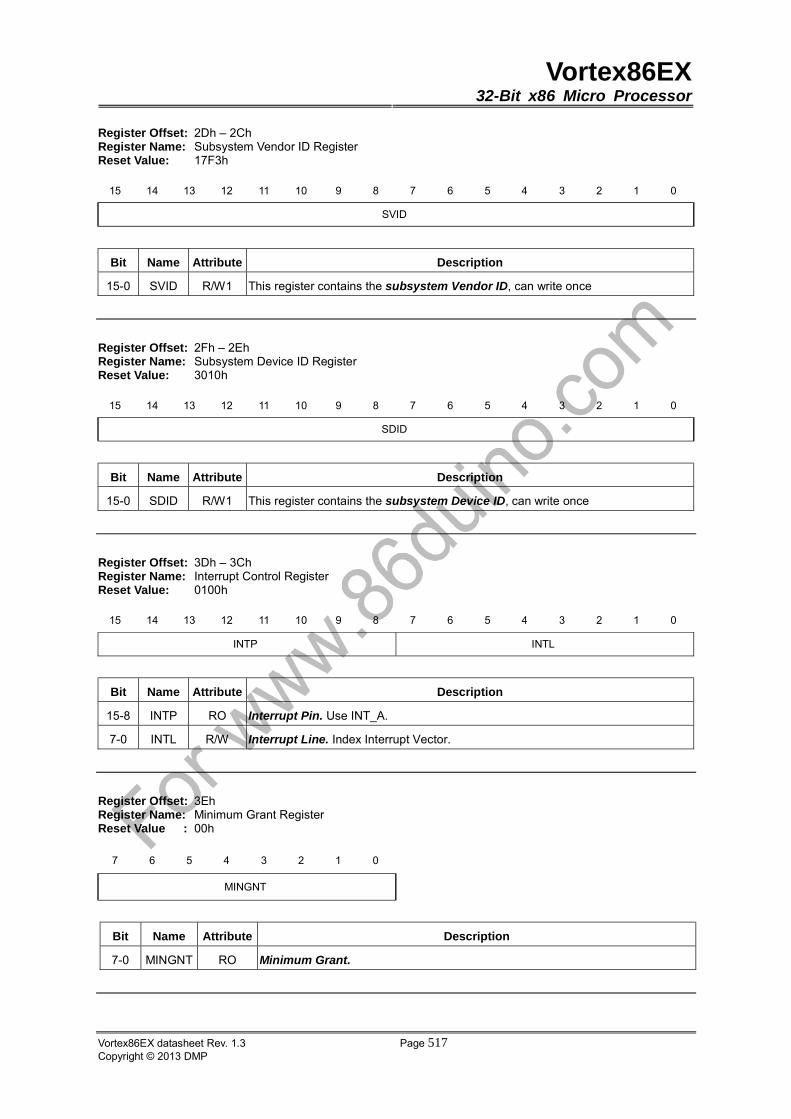
Vortex86EX32-Bit x86 Micro Processor
Vortex86EX datasheet Rev. 1.3 Page 517Copyright © 2013 DMP
Register Offset: 2Dh – 2Ch Register Name: Subsystem Vendor ID Register Reset Value: 17F3h
15 14 13 12 11 10 9 8 7 6 5 4 3 2 1 0
SVID
Bit Name Attribute Description
15-0 SVID R/W1 This register contains the subsystem Vendor ID, can write once
Register Offset: 2Fh – 2Eh Register Name: Subsystem Device ID Register Reset Value: 3010h
15 14 13 12 11 10 9 8 7 6 5 4 3 2 1 0
SDID
Bit Name Attribute Description
15-0 SDID R/W1 This register contains the subsystem Device ID, can write once
Register Offset: 3Dh – 3Ch Register Name: Interrupt Control Register Reset Value: 0100h
15 14 13 12 11 10 9 8 7 6 5 4 3 2 1 0
INTP INTL
Bit Name Attribute Description
15-8 INTP RO Interrupt Pin. Use INT_A.
7-0 INTL R/W Interrupt Line. Index Interrupt Vector.
Register Offset: 3Eh Register Name: Minimum Grant Register Reset Value : 00h
7 6 5 4 3 2 1 0
MINGNT
Bit Name Attribute Description
7-0 MINGNT RO Minimum Grant.
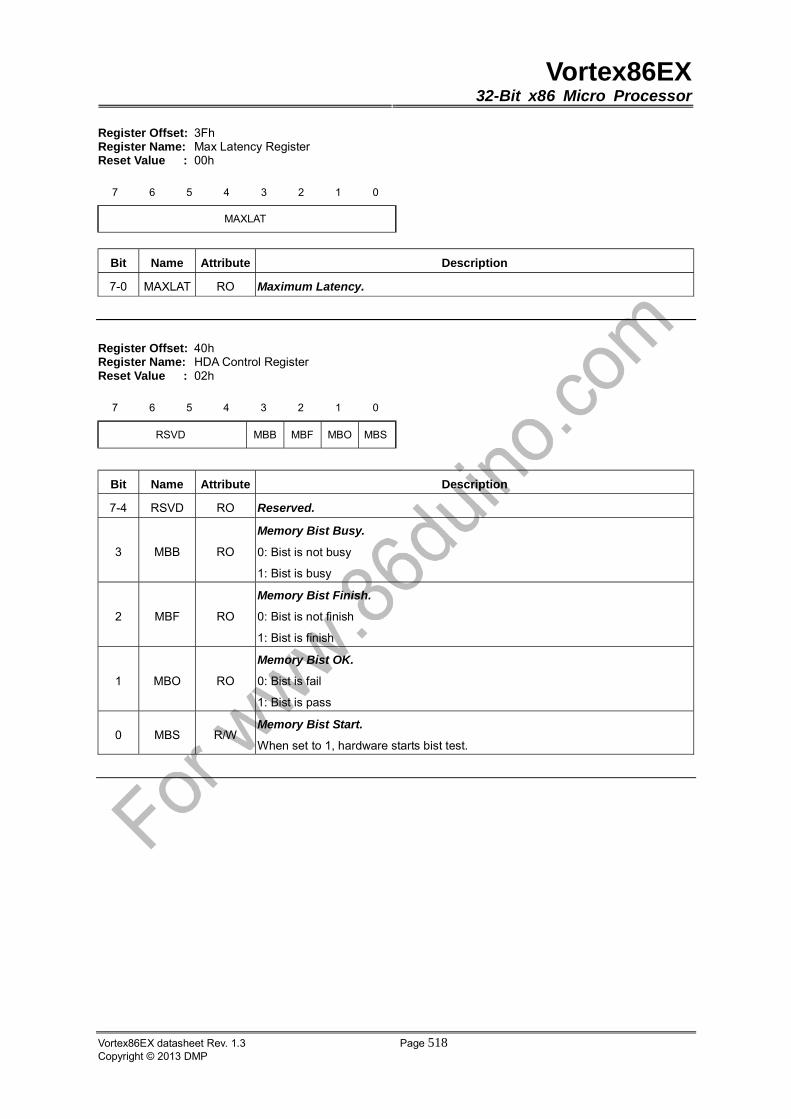
Vortex86EX32-Bit x86 Micro Processor
Vortex86EX datasheet Rev. 1.3 Page 518Copyright © 2013 DMP
Register Offset: 3Fh Register Name: Max Latency Register Reset Value : 00h
7 6 5 4 3 2 1 0
MAXLAT
Bit Name Attribute Description
7-0 MAXLAT RO Maximum Latency.
Register Offset: 40hRegister Name: HDA Control Register Reset Value : 02h
7 6 5 4 3 2 1 0
RSVD MBB MBF MBO MBS
Bit Name Attribute Description
7-4 RSVD RO Reserved.
3 MBB RO
Memory Bist Busy.
0: Bist is not busy
1: Bist is busy
2 MBF RO
Memory Bist Finish.
0: Bist is not finish
1: Bist is finish
1 MBO RO
Memory Bist OK.
0: Bist is fail
1: Bist is pass
0 MBS R/W Memory Bist Start.
When set to 1, hardware starts bist test.
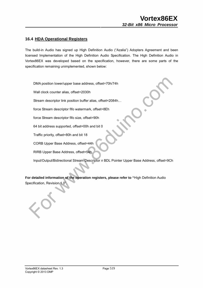
Vortex86EX32-Bit x86 Micro Processor
Vortex86EX datasheet Rev. 1.3 Page 519Copyright © 2013 DMP
16.4 HDA Operational Registers
The build-in Audio has signed up High Definition Audio (“Azalia”) Adopters Agreement and been
licensed Implementation of the High Definition Audio Specification. The High Definition Audio in
Vortex86EX was developed based on the specification, however, there are some parts of the
specification remaining unimplemented, shown below:
DMA position lower/upper base address, offset=70h/74h
Wall clock counter alias, offset=2030h
Stream descriptor link position buffer alias, offset=2084h…
force Stream descriptor fifo watermark, offset=8Eh
force Stream descriptor fifo size, offset=90h
64 bit address supported, offset=00h and bit 0
Traffic priority, offset=80h and bit 18
CORB Upper Base Address, offset=44h
RIRB Upper Base Address, offset=54h
Input/Output/Bidirectional Stream Descriptor n BDL Pointer Upper Base Address, offset=9Ch
For detailed information of the operation registers, please refer to “High Definition Audio
Specification, Revision 1.0”.

Vortex86EX32-Bit x86 Micro Processor
Vortex86EX datasheet Rev. 1.3 Page 520Copyright © 2013 DMP
17. PCI to PCI Express Bridge Control Unit
17.1 Overview
A PCI-to-PCIE bridge provides a connection path between two independent PCI and PCIE buses.
The primary function of the bridge is to allow transactions to occur between a master on one PCI bus
and a target on the other PCIE bus. PCI-to-PCIE bridges provide system and add-in card designers
the ability to overcome electrical loading limits by creating hierarchical PCI buses.
17.2 Features
Support one Port one Lane
Support PCI Express v1.1
17.3 PCI to PCI Express Bridge PCI Configuration Registers Definition
Register Offset: 01h – 00h Register Name: Vendor ID Register Reset Value : 17F3h
15 14 13 12 11 10 9 8 7 6 5 4 3 2 1 0
VID
Bit Name Attribute Description
15-0 VID RO Vendor ID.
Register Offset: 03h – 02h Register Name: Device ID Register Reset Value : 1031h
15 14 13 12 11 10 9 8 7 6 5 4 3 2 1 0
DID
Bit Name Attribute Description
15-0 DID RO Device ID.
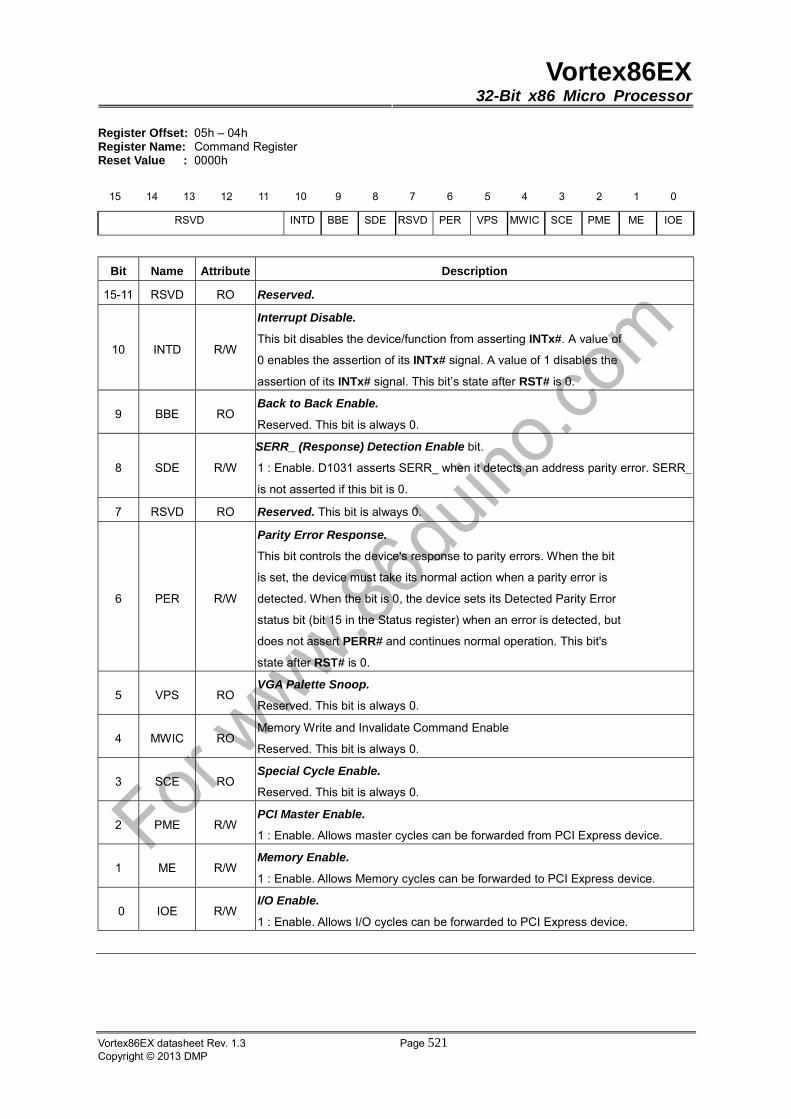
Vortex86EX32-Bit x86 Micro Processor
Vortex86EX datasheet Rev. 1.3 Page 521Copyright © 2013 DMP
Register Offset: 05h – 04h Register Name: Command Register Reset Value : 0000h
15 14 13 12 11 10 9 8 7 6 5 4 3 2 1 0
RSVD INTD BBE SDE RSVD PER VPS MWIC SCE PME ME IOE
Bit Name Attribute Description
15-11 RSVD RO Reserved.
10 INTD R/W
Interrupt Disable.
This bit disables the device/function from asserting INTx#. A value of
0 enables the assertion of its INTx# signal. A value of 1 disables the
assertion of its INTx# signal. This bit’s state after RST# is 0.
9 BBE RO Back to Back Enable.
Reserved. This bit is always 0.
8 SDE R/W
SERR_ (Response) Detection Enable bit.
1 : Enable. D1031 asserts SERR_ when it detects an address parity error. SERR_
is not asserted if this bit is 0.
7 RSVD RO Reserved. This bit is always 0.
6 PER R/W
Parity Error Response.
This bit controls the device's response to parity errors. When the bit
is set, the device must take its normal action when a parity error is
detected. When the bit is 0, the device sets its Detected Parity Error
status bit (bit 15 in the Status register) when an error is detected, but
does not assert PERR# and continues normal operation. This bit's
state after RST# is 0.
5 VPS RO VGA Palette Snoop.
Reserved. This bit is always 0.
4 MWIC RO Memory Write and Invalidate Command Enable
Reserved. This bit is always 0.
3 SCE RO Special Cycle Enable.
Reserved. This bit is always 0.
2 PME R/W PCI Master Enable.
1 : Enable. Allows master cycles can be forwarded from PCI Express device.
1 ME R/W Memory Enable.
1 : Enable. Allows Memory cycles can be forwarded to PCI Express device.
0 IOE R/W I/O Enable.
1 : Enable. Allows I/O cycles can be forwarded to PCI Express device.
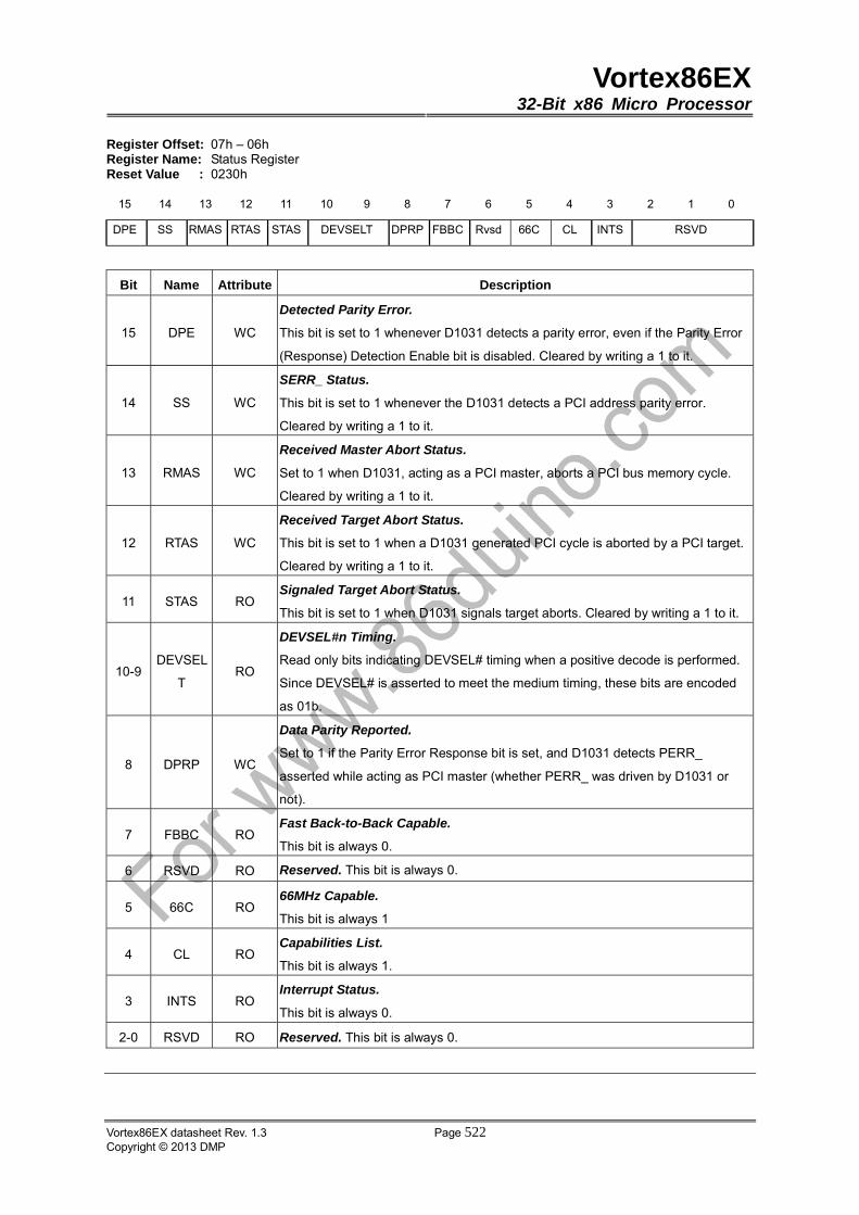
Vortex86EX32-Bit x86 Micro Processor
Vortex86EX datasheet Rev. 1.3 Page 522Copyright © 2013 DMP
Register Offset: 07h – 06h Register Name: Status Register Reset Value : 0230h
15 14 13 12 11 10 9 8 7 6 5 4 3 2 1 0
DPE SS RMAS RTAS STAS DEVSELT DPRP FBBC Rvsd 66C CL INTS RSVD
Bit Name Attribute Description
15 DPE WC
Detected Parity Error.
This bit is set to 1 whenever D1031 detects a parity error, even if the Parity Error
(Response) Detection Enable bit is disabled. Cleared by writing a 1 to it.
14 SS WC
SERR_ Status.
This bit is set to 1 whenever the D1031 detects a PCI address parity error.
Cleared by writing a 1 to it.
13 RMAS WC
Received Master Abort Status.
Set to 1 when D1031, acting as a PCI master, aborts a PCI bus memory cycle.
Cleared by writing a 1 to it.
12 RTAS WC
Received Target Abort Status.
This bit is set to 1 when a D1031 generated PCI cycle is aborted by a PCI target.
Cleared by writing a 1 to it.
11 STAS RO Signaled Target Abort Status.
This bit is set to 1 when D1031 signals target aborts. Cleared by writing a 1 to it.
10-9DEVSEL
T RO
DEVSEL#n Timing.
Read only bits indicating DEVSEL# timing when a positive decode is performed.
Since DEVSEL# is asserted to meet the medium timing, these bits are encoded
as 01b.
8 DPRP WC
Data Parity Reported.
Set to 1 if the Parity Error Response bit is set, and D1031 detects PERR_
asserted while acting as PCI master (whether PERR_ was driven by D1031 or
not).
7 FBBC RO Fast Back-to-Back Capable.
This bit is always 0.
6 RSVD RO Reserved. This bit is always 0.
5 66C RO 66MHz Capable.
This bit is always 1
4 CL RO Capabilities List.
This bit is always 1.
3 INTS RO Interrupt Status.
This bit is always 0.
2-0 RSVD RO Reserved. This bit is always 0.
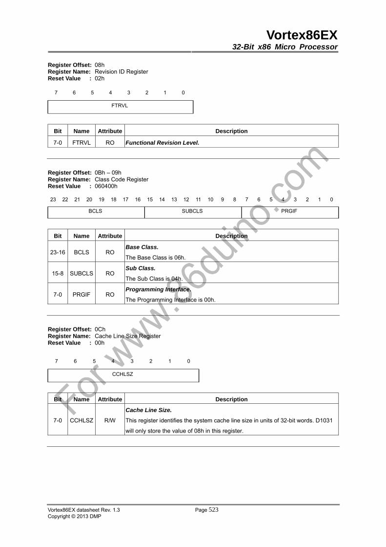
Vortex86EX32-Bit x86 Micro Processor
Vortex86EX datasheet Rev. 1.3 Page 523Copyright © 2013 DMP
Register Offset: 08h Register Name: Revision ID Register Reset Value : 02h
7 6 5 4 3 2 1 0
FTRVL
Bit Name Attribute Description
7-0 FTRVL RO Functional Revision Level.
Register Offset: 0Bh – 09h Register Name: Class Code Register Reset Value : 060400h
23 22 21 20 19 18 17 16 15 14 13 12 11 10 9 8 7 6 5 4 3 2 1 0
BCLS SUBCLS PRGIF
Bit Name Attribute Description
23-16 BCLS RO Base Class.
The Base Class is 06h.
15-8 SUBCLS RO Sub Class.
The Sub Class is 04h.
7-0 PRGIF RO Programming Interface.
The Programming Interface is 00h.
Register Offset: 0Ch Register Name: Cache Line Size Register Reset Value : 00h
7 6 5 4 3 2 1 0
CCHLSZ
Bit Name Attribute Description
7-0 CCHLSZ R/W
Cache Line Size.
This register identifies the system cache line size in units of 32-bit words. D1031
will only store the value of 08h in this register.
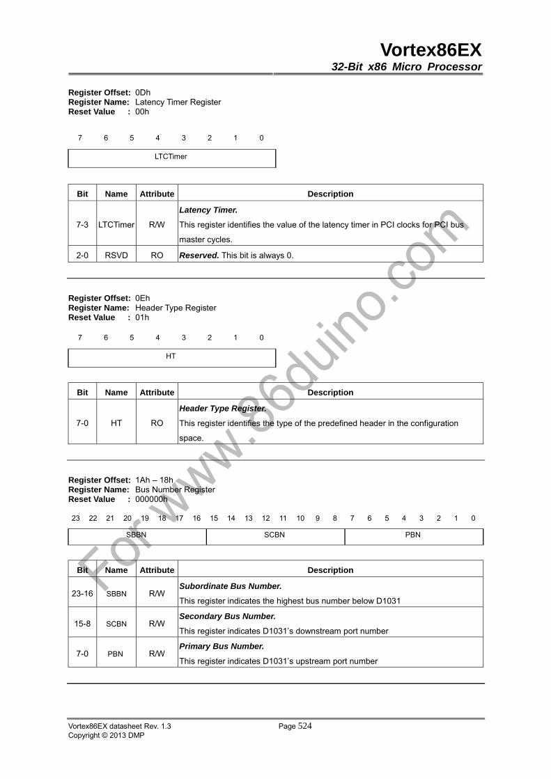
Vortex86EX32-Bit x86 Micro Processor
Vortex86EX datasheet Rev. 1.3 Page 524Copyright © 2013 DMP
Register Offset: 0Dh Register Name: Latency Timer Register Reset Value : 00h
7 6 5 4 3 2 1 0
LTCTimer
Bit Name Attribute Description
7-3 LTCTimer R/W
Latency Timer.
This register identifies the value of the latency timer in PCI clocks for PCI bus
master cycles.
2-0 RSVD RO Reserved. This bit is always 0.
Register Offset: 0Eh Register Name: Header Type Register Reset Value : 01h
7 6 5 4 3 2 1 0
HT
Bit Name Attribute Description
7-0 HT RO
Header Type Register.
This register identifies the type of the predefined header in the configuration
space.
Register Offset: 1Ah – 18h Register Name: Bus Number Register Reset Value : 000000h
23 22 21 20 19 18 17 16 15 14 13 12 11 10 9 8 7 6 5 4 3 2 1 0
SBBN SCBN PBN
Bit Name Attribute Description
23-16 SBBN R/W Subordinate Bus Number.
This register indicates the highest bus number below D1031
15-8 SCBN R/W Secondary Bus Number.
This register indicates D1031’s downstream port number
7-0 PBN R/W Primary Bus Number.
This register indicates D1031’s upstream port number
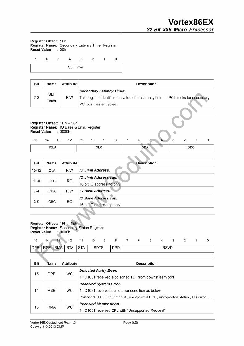
Vortex86EX32-Bit x86 Micro Processor
Vortex86EX datasheet Rev. 1.3 Page 525Copyright © 2013 DMP
Register Offset: 1Bh Register Name: Secondary Latency Timer Register Reset Value : 00h
7 6 5 4 3 2 1 0
SLT Timer
Bit Name Attribute Description
7-3SLT
Timer R/W
Secondary Latency Timer.
This register identifies the value of the latency timer in PCI clocks for secondary
PCI bus master cycles.
Register Offset: 1Dh – 1Ch Register Name: IO Base & Limit Register Reset Value : 0000h
15 14 13 12 11 10 9 8 7 6 5 4 3 2 1 0
IOLA IOLC IOBA IOBC
Bit Name Attribute Description
15-12 IOLA R/W IO Limit Address.
11-8 IOLC RO IO Limit Address cap.
16 bit IO addressing only
7-4 IOBA R/W IO Base Address.
3-0 IOBC RO IO Base Address cap.
16 bit IO addressing only
Register Offset: 1Fh – 1Eh Register Name: Secondary Status Register Reset Value : 0000h
15 14 13 12 11 10 9 8 7 6 5 4 3 2 1 0
DPE RSE RMA RTA STA SDTS DPD RSVD
Bit Name Attribute Description
15 DPE WC Detected Parity Error.
1 : D1031 received a poisoned TLP from downstream port
14 RSE WC
Received System Error.
1 : D1031 received some error condition as below
Poisoned TLP , CPL timeout , unexpected CPL , unexpected status , FC error….
13 RMA WC Received Master Abort.
1 : D1031 received CPL with “Unsupported Request”
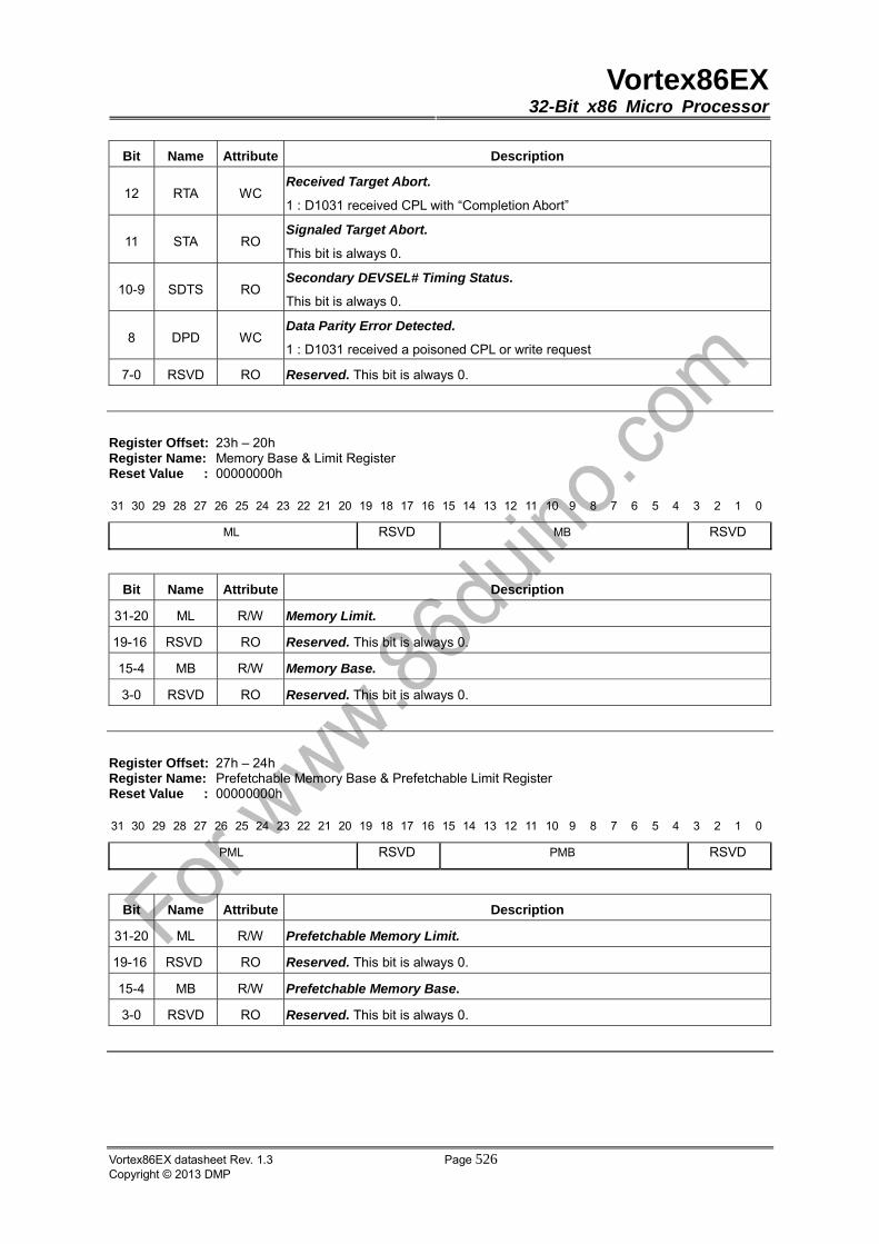
Vortex86EX32-Bit x86 Micro Processor
Vortex86EX datasheet Rev. 1.3 Page 526Copyright © 2013 DMP
Bit Name Attribute Description
12 RTA WC Received Target Abort.
1 : D1031 received CPL with “Completion Abort”
11 STA RO Signaled Target Abort.
This bit is always 0.
10-9 SDTS RO Secondary DEVSEL# Timing Status.
This bit is always 0.
8 DPD WC Data Parity Error Detected.
1 : D1031 received a poisoned CPL or write request
7-0 RSVD RO Reserved. This bit is always 0.
Register Offset: 23h – 20h Register Name: Memory Base & Limit Register Reset Value : 00000000h
31 30 29 28 27 26 25 24 23 22 21 20 19 18 17 16 15 14 13 12 11 10 9 8 7 6 5 4 3 2 1 0
ML RSVD MB RSVD
Bit Name Attribute Description
31-20 ML R/W Memory Limit.
19-16 RSVD RO Reserved. This bit is always 0.
15-4 MB R/W Memory Base.
3-0 RSVD RO Reserved. This bit is always 0.
Register Offset: 27h – 24h Register Name: Prefetchable Memory Base & Prefetchable Limit Register Reset Value : 00000000h
31 30 29 28 27 26 25 24 23 22 21 20 19 18 17 16 15 14 13 12 11 10 9 8 7 6 5 4 3 2 1 0
PML RSVD PMB RSVD
Bit Name Attribute Description
31-20 ML R/W Prefetchable Memory Limit.
19-16 RSVD RO Reserved. This bit is always 0.
15-4 MB R/W Prefetchable Memory Base.
3-0 RSVD RO Reserved. This bit is always 0.

Vortex86EX32-Bit x86 Micro Processor
Vortex86EX datasheet Rev. 1.3 Page 527Copyright © 2013 DMP
Register Offset: 34h Register Name: Capabilities List Pointer Register Reset Value : 40h
7 6 5 4 3 2 1 0
PTR
Bit Name Attribute Description
7-0 PTR RO Capabilities List Pointer.
Register Offset: 3Dh – 3Ch Register Name: Interrupt Control Register Reset Value: 01FFh
15 14 13 12 11 10 9 8 7 6 5 4 3 2 1 0
INTP INTL
Bit Name Attribute Description
15-8 INTP RO Interrupt Pin. Use INT_A.
7-0 INTL R/W Interrupt Line. Index Interrupt Vector.
Register Offset: 3Fh – 3Eh Register Name: Minimum Grant Register Reset Value : 0000h
15 14 13 12 11 10 9 8 7 6 5 4 3 2 1 0
RSVD SBR RSVD V16 VE IE SE PERE
Bit Name Attribute Description
15-7 RSVD RO Reserved. This bit is always 0.
6 SBR R/W Secondary Bus Reset.
1 : trigger reset on downstream port
5 RSVD RO Reserved. This bit is always 0.
4 V16 R/W VGA 16 bit Decode.
1 : execute 16 bit address decodes on VGA IO accesses
3 VE R/W
VGA Enable.
1 : forward VGA compatible memory and IO addresses from primary IF to
secondary IF
2 IE RO Reserved. This bit is always 0
1 SE R/W SERR# Enable.
0 PERE R/W Parity Error Response Enable.
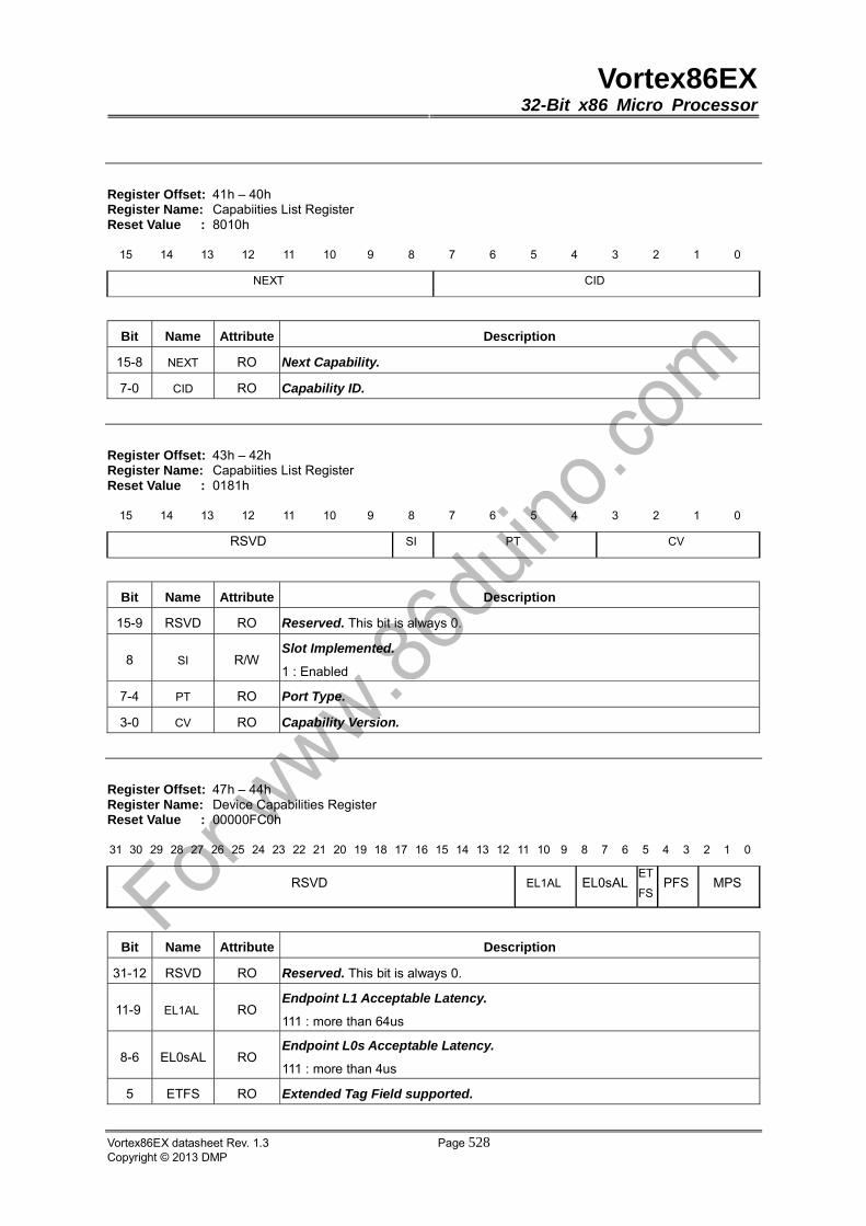
Vortex86EX32-Bit x86 Micro Processor
Vortex86EX datasheet Rev. 1.3 Page 528Copyright © 2013 DMP
Register Offset: 41h – 40h Register Name: Capabiities List Register Reset Value : 8010h
15 14 13 12 11 10 9 8 7 6 5 4 3 2 1 0
NEXT CID
Bit Name Attribute Description
15-8 NEXT RO Next Capability.
7-0 CID RO Capability ID.
Register Offset: 43h – 42h Register Name: Capabiities List Register Reset Value : 0181h
15 14 13 12 11 10 9 8 7 6 5 4 3 2 1 0
RSVD SI PT CV
Bit Name Attribute Description
15-9 RSVD RO Reserved. This bit is always 0.
8 SI R/W Slot Implemented.
1 : Enabled
7-4 PT RO Port Type.
3-0 CV RO Capability Version.
Register Offset: 47h – 44h Register Name: Device Capabilities Register Reset Value : 00000FC0h
31 30 29 28 27 26 25 24 23 22 21 20 19 18 17 16 15 14 13 12 11 10 9 8 7 6 5 4 3 2 1 0
RSVD EL1AL EL0sALET
FSPFS MPS
Bit Name Attribute Description
31-12 RSVD RO Reserved. This bit is always 0.
11-9 EL1AL RO Endpoint L1 Acceptable Latency.
111 : more than 64us
8-6 EL0sAL RO Endpoint L0s Acceptable Latency.
111 : more than 4us
5 ETFS RO Extended Tag Field supported.
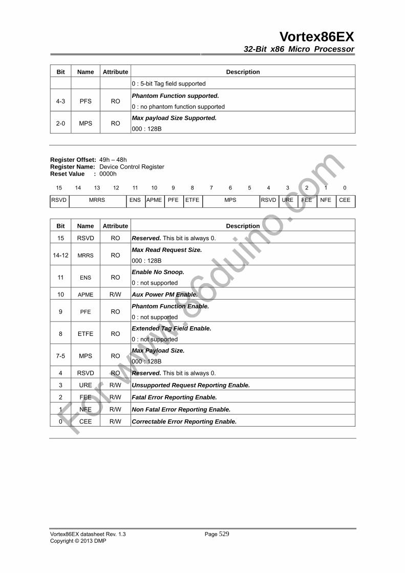
Vortex86EX32-Bit x86 Micro Processor
Vortex86EX datasheet Rev. 1.3 Page 529Copyright © 2013 DMP
Bit Name Attribute Description
0 : 5-bit Tag field supported
4-3 PFS RO Phantom Function supported.
0 : no phantom function supported
2-0 MPS RO Max payload Size Supported.
000 : 128B
Register Offset: 49h – 48h Register Name: Device Control Register Reset Value : 0000h
15 14 13 12 11 10 9 8 7 6 5 4 3 2 1 0
RSVD MRRS ENS APME PFE ETFE MPS RSVD URE FEE NFE CEE
Bit Name Attribute Description
15 RSVD RO Reserved. This bit is always 0.
14-12 MRRS RO Max Read Request Size.
000 : 128B
11 ENS RO Enable No Snoop.
0 : not supported
10 APME R/W Aux Power PM Enable.
9 PFE RO Phantom Function Enable.
0 : not supported
8 ETFE RO Extended Tag Field Enable.
0 : not supported
7-5 MPS RO Max Payload Size.
000 : 128B
4 RSVD RO Reserved. This bit is always 0.
3 URE R/W Unsupported Request Reporting Enable.
2 FEE R/W Fatal Error Reporting Enable.
1 NFE R/W Non Fatal Error Reporting Enable.
0 CEE R/W Correctable Error Reporting Enable.

Vortex86EX32-Bit x86 Micro Processor
Vortex86EX datasheet Rev. 1.3 Page 530Copyright © 2013 DMP
Register Offset: 4Bh – 4Ah Register Name: Device Status Register Reset Value : 0010h
15 14 13 12 11 10 9 8 7 6 5 4 3 2 1 0
RSVD TDP APD URD FED NFED CED
Bit Name Attribute Description
15-6 RSVD RO Reserved. This bit is always 0.
5 TDP RO Transactions Pending.
4 APD RO AUX Power Detected.
3 URD WC Unsupported Request Detected.
2 FED WC Fatal Error Detected.
1 NFED WC Non Fatal Error Detected.
0 CED WC Correctable Error Detected.
Register Offset: 4Fh – 4Ch Register Name: Link Capabilities Register Reset Value : 0?12DC11h
31 30 29 28 27 26 25 24 23 22 21 20 19 18 17 16 15 14 13 12 11 10 9 8 7 6 5 4 3 2 1 0
PN RSVDLA
CRSVD L1EL L0EL
APM
SMLW MLS
Bit Name Attribute Description
31-24 PN R/W Port Number.
By implemented port
23-21 RSVD RO Reserved. This bit is always 0.
20 LAC RO Link Active Reporting Capable.
19-18 RSVD RO Reserved. This bit is always 0.
17-15 L1EL RO L1 Exit Latency.
101 : 16us to less than 32us
14-12 L0EL RO L0s Exit Latency.
101 : 1us to less than 2us
11-10 APMS RO Active State Link PM Support.
11 : L0s and L1 supported
9-4 MLW RO Max Link Width.
1 : x1
3-0 MLS RO Max Link Speed.
1 : 2.5Gb/s
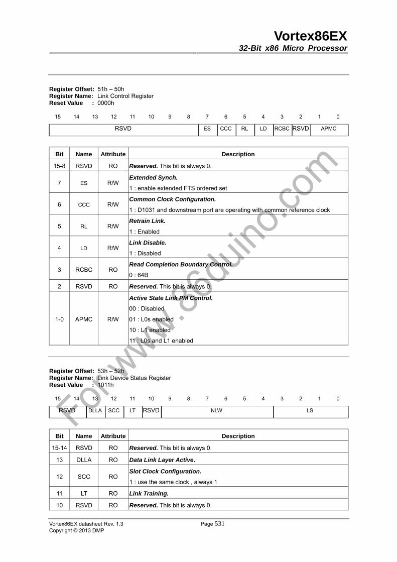
Vortex86EX32-Bit x86 Micro Processor
Vortex86EX datasheet Rev. 1.3 Page 531Copyright © 2013 DMP
Register Offset: 51h – 50h Register Name: Link Control Register Reset Value : 0000h
15 14 13 12 11 10 9 8 7 6 5 4 3 2 1 0
RSVD ES CCC RL LD RCBC RSVD APMC
Bit Name Attribute Description
15-8 RSVD RO Reserved. This bit is always 0.
7 ES R/W Extended Synch.
1 : enable extended FTS ordered set
6 CCC R/W Common Clock Configuration.
1 : D1031 and downstream port are operating with common reference clock
5 RL R/W Retrain Link.
1 : Enabled
4 LD R/W Link Disable.
1 : Disabled
3 RCBC RO Read Completion Boundary Control.
0 : 64B
2 RSVD RO Reserved. This bit is always 0.
1-0 APMC R/W
Active State Link PM Control.
00 : Disabled
01 : L0s enabled
10 : L1 enabled
11 : L0s and L1 enabled
Register Offset: 53h – 52h Register Name: Link Device Status Register Reset Value : 1011h
15 14 13 12 11 10 9 8 7 6 5 4 3 2 1 0
RSVD DLLA SCC LT RSVD NLW LS
Bit Name Attribute Description
15-14 RSVD RO Reserved. This bit is always 0.
13 DLLA RO Data Link Layer Active.
12 SCC RO Slot Clock Configuration.
1 : use the same clock , always 1
11 LT RO Link Training.
10 RSVD RO Reserved. This bit is always 0.
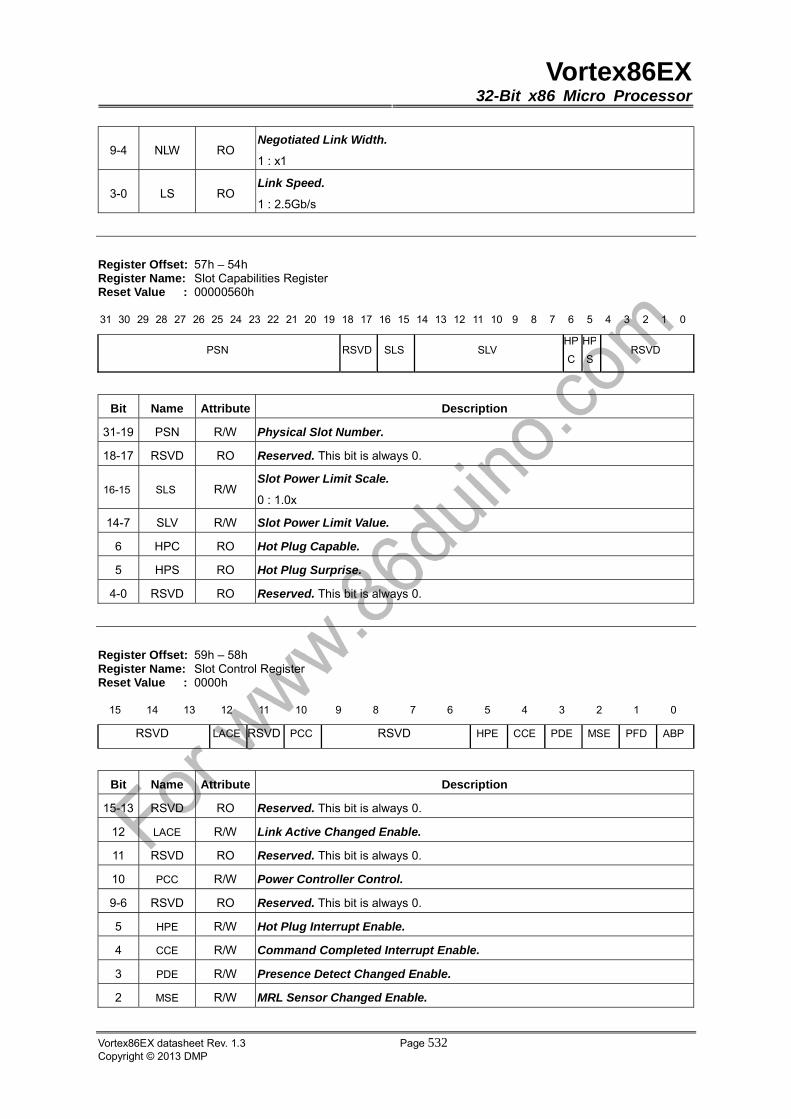
Vortex86EX32-Bit x86 Micro Processor
Vortex86EX datasheet Rev. 1.3 Page 532Copyright © 2013 DMP
9-4 NLW RO Negotiated Link Width.
1 : x1
3-0 LS RO Link Speed.
1 : 2.5Gb/s
Register Offset: 57h – 54h Register Name: Slot Capabilities Register Reset Value : 00000560h
31 30 29 28 27 26 25 24 23 22 21 20 19 18 17 16 15 14 13 12 11 10 9 8 7 6 5 4 3 2 1 0
PSN RSVD SLS SLV HP
C
HP
SRSVD
Bit Name Attribute Description
31-19 PSN R/W Physical Slot Number.
18-17 RSVD RO Reserved. This bit is always 0.
16-15 SLS R/W Slot Power Limit Scale.
0 : 1.0x
14-7 SLV R/W Slot Power Limit Value.
6 HPC RO Hot Plug Capable.
5 HPS RO Hot Plug Surprise.
4-0 RSVD RO Reserved. This bit is always 0.
Register Offset: 59h – 58h Register Name: Slot Control Register Reset Value : 0000h
15 14 13 12 11 10 9 8 7 6 5 4 3 2 1 0
RSVD LACE RSVD PCC RSVD HPE CCE PDE MSE PFD ABP
Bit Name Attribute Description
15-13 RSVD RO Reserved. This bit is always 0.
12 LACE R/W Link Active Changed Enable.
11 RSVD RO Reserved. This bit is always 0.
10 PCC R/W Power Controller Control.
9-6 RSVD RO Reserved. This bit is always 0.
5 HPE R/W Hot Plug Interrupt Enable.
4 CCE R/W Command Completed Interrupt Enable.
3 PDE R/W Presence Detect Changed Enable.
2 MSE R/W MRL Sensor Changed Enable.
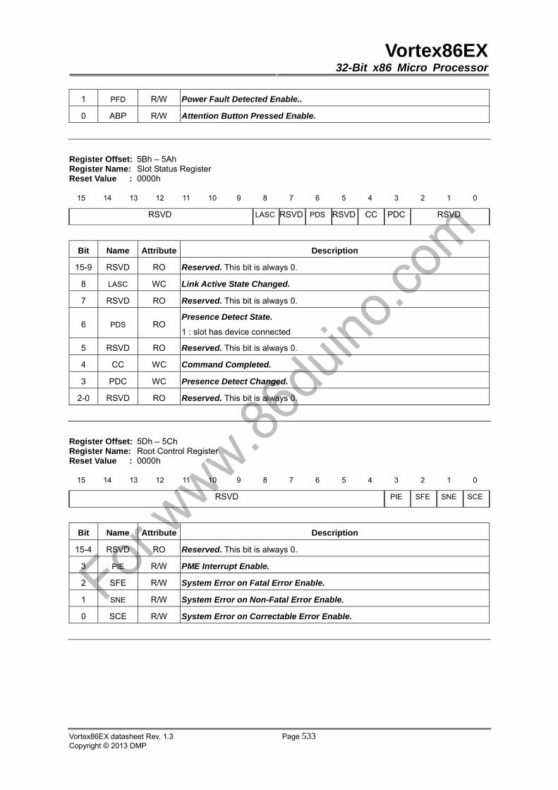
Vortex86EX32-Bit x86 Micro Processor
Vortex86EX datasheet Rev. 1.3 Page 533Copyright © 2013 DMP
1 PFD R/W Power Fault Detected Enable..
0 ABP R/W Attention Button Pressed Enable.
Register Offset: 5Bh – 5Ah Register Name: Slot Status Register Reset Value : 0000h
15 14 13 12 11 10 9 8 7 6 5 4 3 2 1 0
RSVD LASC RSVD PDS RSVD CC PDC RSVD
Bit Name Attribute Description
15-9 RSVD RO Reserved. This bit is always 0.
8 LASC WC Link Active State Changed.
7 RSVD RO Reserved. This bit is always 0.
6 PDS RO Presence Detect State.
1 : slot has device connected
5 RSVD RO Reserved. This bit is always 0.
4 CC WC Command Completed.
3 PDC WC Presence Detect Changed.
2-0 RSVD RO Reserved. This bit is always 0.
Register Offset: 5Dh – 5Ch Register Name: Root Control Register Reset Value : 0000h
15 14 13 12 11 10 9 8 7 6 5 4 3 2 1 0
RSVD PIE SFE SNE SCE
Bit Name Attribute Description
15-4 RSVD RO Reserved. This bit is always 0.
3 PIE R/W PME Interrupt Enable.
2 SFE R/W System Error on Fatal Error Enable.
1 SNE R/W System Error on Non-Fatal Error Enable.
0 SCE R/W System Error on Correctable Error Enable.
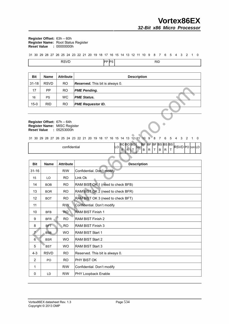
Vortex86EX32-Bit x86 Micro Processor
Vortex86EX datasheet Rev. 1.3 Page 534Copyright © 2013 DMP
Register Offset: 63h – 60h Register Name: Root Status Register Reset Value : 00000000h
31 30 29 28 27 26 25 24 23 22 21 20 19 18 17 16 15 14 13 12 11 10 9 8 7 6 5 4 3 2 1 0
RSVD PP PS RID
Bit Name Attribute Description
31-18 RSVD RO Reserved. This bit is always 0.
17 PP RO PME Pending.
16 PS WC PME Status.
15-0 RID RO PME Requestor ID.
Register Offset: 67h – 64hRegister Name: MISC Register Reset Value : 05253000h
31 30 29 28 27 26 25 24 23 22 21 20 19 18 17 16 15 14 13 12 11 10 9 8 7 6 5 4 3 2 1 0
confidential LOBO
B
BO
R
BO
Tcon
BF
B
BF
R
BF
T
BS
B
BS
R
BS
TRSVD PO con LD
Bit Name Attribute Description
31-16 R/W Confidential. Don’t modify
15 LO RO Link Ok
14 BOB RO RAM BIST OK 1 (need to check BFB)
13 BOR RO RAM BIST OK 2 (need to check BFR)
12 BOT RO RAM BIST OK 3 (need to check BFT)
11 R/W Confidential. Don’t modify
10 BFB RO RAM BIST Finish 1
9 BFR RO RAM BIST Finish 2
8 BFT RO RAM BIST Finish 3
7 BSB WO RAM BIST Start 1
6 BSR WO RAM BIST Start 2
5 BST WO RAM BIST Start 3
4-3 RSVD RO Reserved. This bit is always 0.
2 PO RO PHY BIST OK
1 R/W Confidential. Don’t modify
0 LD R/W PHY Loopback Enable
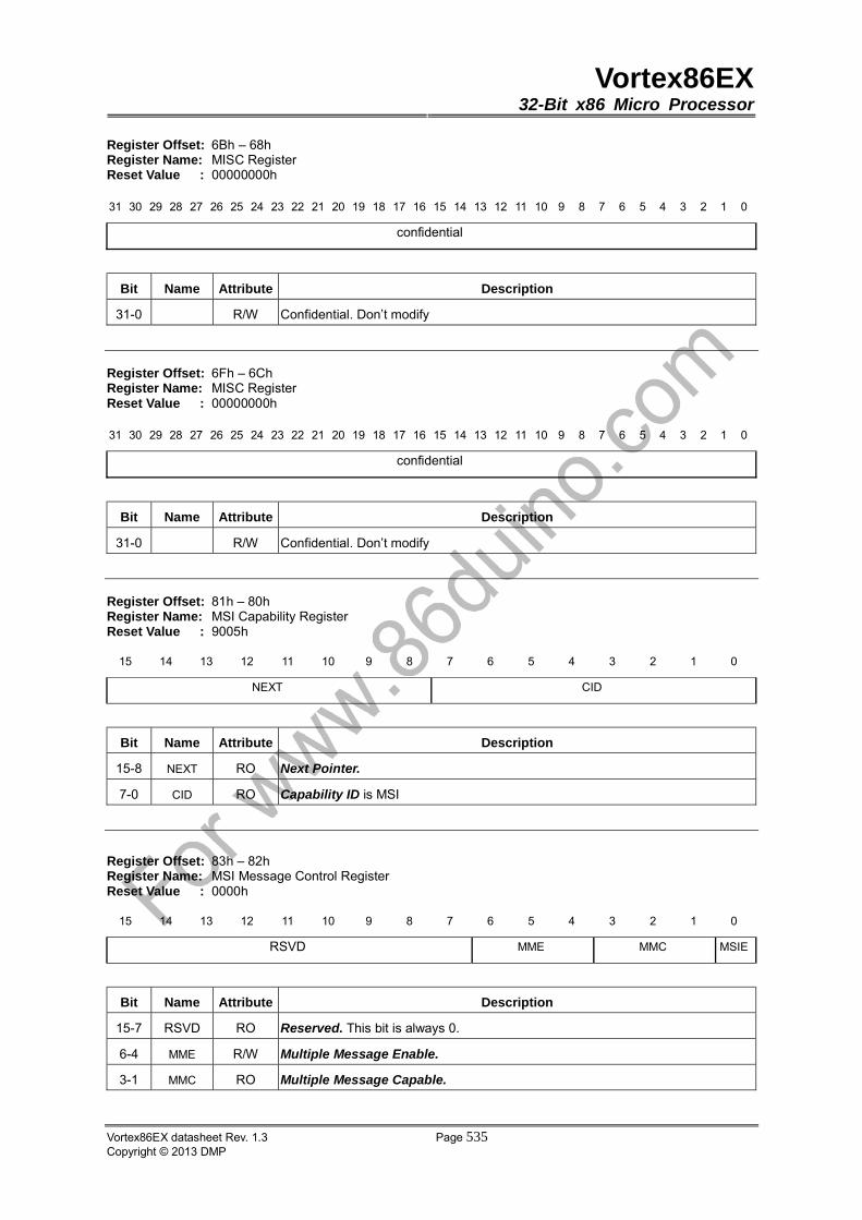
Vortex86EX32-Bit x86 Micro Processor
Vortex86EX datasheet Rev. 1.3 Page 535Copyright © 2013 DMP
Register Offset: 6Bh – 68h Register Name: MISC Register Reset Value : 00000000h
31 30 29 28 27 26 25 24 23 22 21 20 19 18 17 16 15 14 13 12 11 10 9 8 7 6 5 4 3 2 1 0
confidential
Bit Name Attribute Description
31-0 R/W Confidential. Don’t modify
Register Offset: 6Fh – 6Ch Register Name: MISC Register Reset Value : 00000000h
31 30 29 28 27 26 25 24 23 22 21 20 19 18 17 16 15 14 13 12 11 10 9 8 7 6 5 4 3 2 1 0
confidential
Bit Name Attribute Description
31-0 R/W Confidential. Don’t modify
Register Offset: 81h – 80h Register Name: MSI Capability Register Reset Value : 9005h
15 14 13 12 11 10 9 8 7 6 5 4 3 2 1 0
NEXT CID
Bit Name Attribute Description
15-8 NEXT RO Next Pointer.
7-0 CID RO Capability ID is MSI
Register Offset: 83h – 82h Register Name: MSI Message Control Register Reset Value : 0000h
15 14 13 12 11 10 9 8 7 6 5 4 3 2 1 0
RSVD MME MMC MSIE
Bit Name Attribute Description
15-7 RSVD RO Reserved. This bit is always 0.
6-4 MME R/W Multiple Message Enable.
3-1 MMC RO Multiple Message Capable.

Vortex86EX32-Bit x86 Micro Processor
Vortex86EX datasheet Rev. 1.3 Page 536Copyright © 2013 DMP
0 MSIE R/W MSI Enable.
Register Offset: 87h – 84h Register Name: MSI Message Address Register Reset Value : 00000000h
31 30 29 28 27 26 25 24 23 22 21 20 19 18 17 16 15 14 13 12 11 10 9 8 7 6 5 4 3 2 1 0
ADDR RSVD
Bit Name Attribute Description
31-2 ADDR R/W Address for message address
1-0 RSVD RO Reserved. This bit is always 0.
Register Offset: 89h – 88h Register Name: MSI Message Data Register Reset Value : 0000h
15 14 13 12 11 10 9 8 7 6 5 4 3 2 1 0
DATA
Bit Name Attribute Description
15-0 DATA R/W Programmed by system
Register Offset: 91h – 90h Register Name: PM Capability Register Reset Value : 0001h
15 14 13 12 11 10 9 8 7 6 5 4 3 2 1 0
NEXT CID
Bit Name Attribute Description
15-8 NEXT RO Next Pointer. The last item.
7-0 CID RO Capability ID is PM.

Vortex86EX32-Bit x86 Micro Processor
Vortex86EX datasheet Rev. 1.3 Page 537Copyright © 2013 DMP
Register Offset: 93h – 92h Register Name: PCI PM Capability Register Reset Value : C802h
15 14 13 12 11 10 9 8 7 6 5 4 3 2 1 0
PMES RSVD AC DSI RSVD PMEC VS
Bit Name Attribute Description
15-11 PMES RO PME_Support.
10-9 RSVD RO Reserved. This bit is always 0.
8-6 AC RO Aux_Current.
5 DSI RO Device Specific Initialization.
4 RSVD RO Reserved. This bit is always 0.
3 PMEC RO PME Clock.
2-0 VS RO Version.
Register Offset: 97h – 94h Register Name: PCI PM Control & Status Register Reset Value : 00000000h
31 30 29 28 27 26 25 24 23 22 21 20 19 18 17 16 15 14 13 12 11 10 9 8 7 6 5 4 3 2 1 0
RSVDPM
ESRSVD
PM
EERSVD PS
Bit Name Attribute Description
31-16 RSVD RO Reserved. This bit is always 0.
15 PMES RO PME Status.
14-9 RSVD RO Reserved. This bit is always 0.
8 PMEE R/W PME Enable.
7-2 RSVD RO Reserved. This bit is always 0.
1-0 PS R/W
Power State.
00 : D0 state
11 : D3 hot state
Vortex86EX32-Bit x86 Micro Processor
Vortex86EX datasheet Rev. 1.3 Page 538Copyright © 2013 DMP
18. CAN Controller
18.1 Overview
The CAN controller, which is compatible with the CAN2.0A/2.0B specification .It supports 2 CAN Bus
channels.
18.2 Features
� CAN Functions
– Compatible with the CAN 2.0A/2.0B specification and supports two CAN Bus channels
– Supports speed up to 1MHz.
– Programmable hardware arbitration lost retry function and hardware error retry function
� PCI Interface
– Host interface compiles with PCI local bus specification revision 2.2
– Supports PCI Power Management v1.1 capability
– Support one Flash/ROM interface for expansion ROM of PCI card

Vortex86EX32-Bit x86 Micro Processor
Vortex86EX datasheet Rev. 1.3 Page 539Copyright © 2013 DMP
18.3 List of PCI Configuration Registers
31 16 15 00 Index
Device ID (1070h) Vendor ID (17F3h) 00h-03h
Status (0200h) Command (0000h) 04h-07h
Base Class Code
(0Ch)
Sub-class code
(09h)
Program Interface
(00h) Revision ID (00h) 08h-0Bh
Reserved Header Type (00h)Latency Timer
(00h)
Cache Line Size
(00h) 0Ch-0Fh
CAN Bus Control/Status Block Register Base Address (MEMORY SPACE) 10h-13h
CAN Bus Control/Status Block Register Base Address (IO SPACE) 14h-17h
Reserved 18h-2Bh
Sub-system Device ID (1070h) Sub-system Vendor ID (17F3h) 2Ch-2Fh
Reserved 30h-3Bh
MAX_LAT (00h) MIN_GNT (00h) INTERRUPT PIN
(01h)
INTERRUPT LINE
(ffh) 3Ch-3Fh
Reserved 40h-FFh

Vortex86EX32-Bit x86 Micro Processor
Vortex86EX datasheet Rev. 1.3 Page 540Copyright © 2013 DMP
18.4 PCI Configuration Registers Definition
Register Offset: 00h Register Name: PCI PM Capability Register Reset Value : 17F3h
15 14 13 12 11 10 9 8 7 6 5 4 3 2 1 0
VID
Bit Name Attribute Description
15-0 VID RO Vendor ID.
This is a 16-bit value assigned to the ITE IDE Controller function.
Register Offset: 02h Register Name: PCI PM Capability Register Reset Value : 1070h
15 14 13 12 11 10 9 8 7 6 5 4 3 2 1 0
DID
Bit Name Attribute Description
15-0 VID RO Device ID.
This is a 16-bit value assigned to the ITE IDE Controller function.
Register Offset: 04h Register Name: Command Register Reset Value : 0000h
15 14 13 12 11 10 9 8 7 6 5 4 3 2 1 0
Bit Name Attribute Description
15-11 RSVD RO Reserved.
10 ID R/W
Interrupt Disable.
1: Enabled
0: Disabled
9 RSVD RO Reserved.
8 SERRFE R/W SERR# Function Enable.
1: Enabled
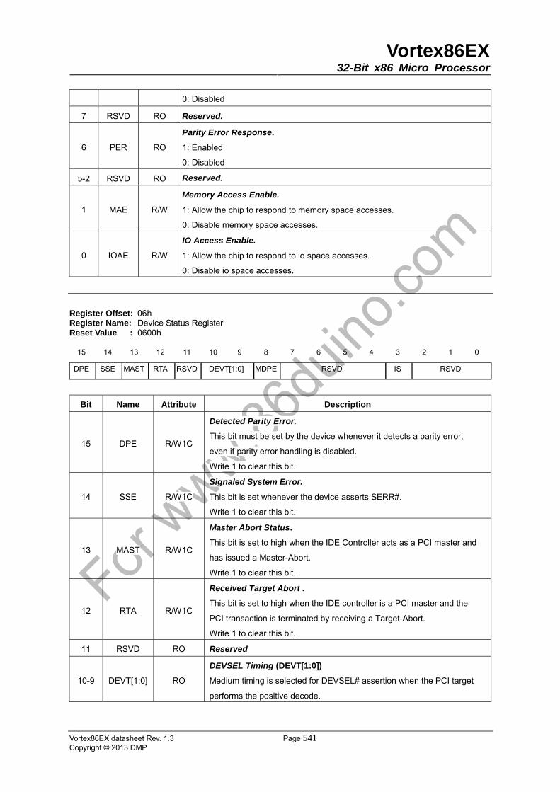
Vortex86EX32-Bit x86 Micro Processor
Vortex86EX datasheet Rev. 1.3 Page 541Copyright © 2013 DMP
0: Disabled
7 RSVD RO Reserved.
6 PER RO
Parity Error Response.
1: Enabled
0: Disabled
5-2 RSVD RO Reserved.
1 MAE R/W
Memory Access Enable.
1: Allow the chip to respond to memory space accesses.
0: Disable memory space accesses.
0 IOAE R/W
IO Access Enable.
1: Allow the chip to respond to io space accesses.
0: Disable io space accesses.
Register Offset: 06h Register Name: Device Status Register Reset Value : 0600h
15 14 13 12 11 10 9 8 7 6 5 4 3 2 1 0
DPE SSE MAST RTA RSVD DEVT[1:0] MDPE RSVD IS RSVD
Bit Name Attribute Description
15 DPE R/W1C
Detected Parity Error.
This bit must be set by the device whenever it detects a parity error,
even if parity error handling is disabled.
Write 1 to clear this bit.
14 SSE R/W1C
Signaled System Error.
This bit is set whenever the device asserts SERR#.
Write 1 to clear this bit.
13 MAST R/W1C
Master Abort Status.
This bit is set to high when the IDE Controller acts as a PCI master and
has issued a Master-Abort.
Write 1 to clear this bit.
12 RTA R/W1C
Received Target Abort .
This bit is set to high when the IDE controller is a PCI master and the
PCI transaction is terminated by receiving a Target-Abort.
Write 1 to clear this bit.
11 RSVD RO Reserved
10-9 DEVT[1:0] RO
DEVSEL Timing (DEVT[1:0])
Medium timing is selected for DEVSEL# assertion when the PCI target
performs the positive decode.
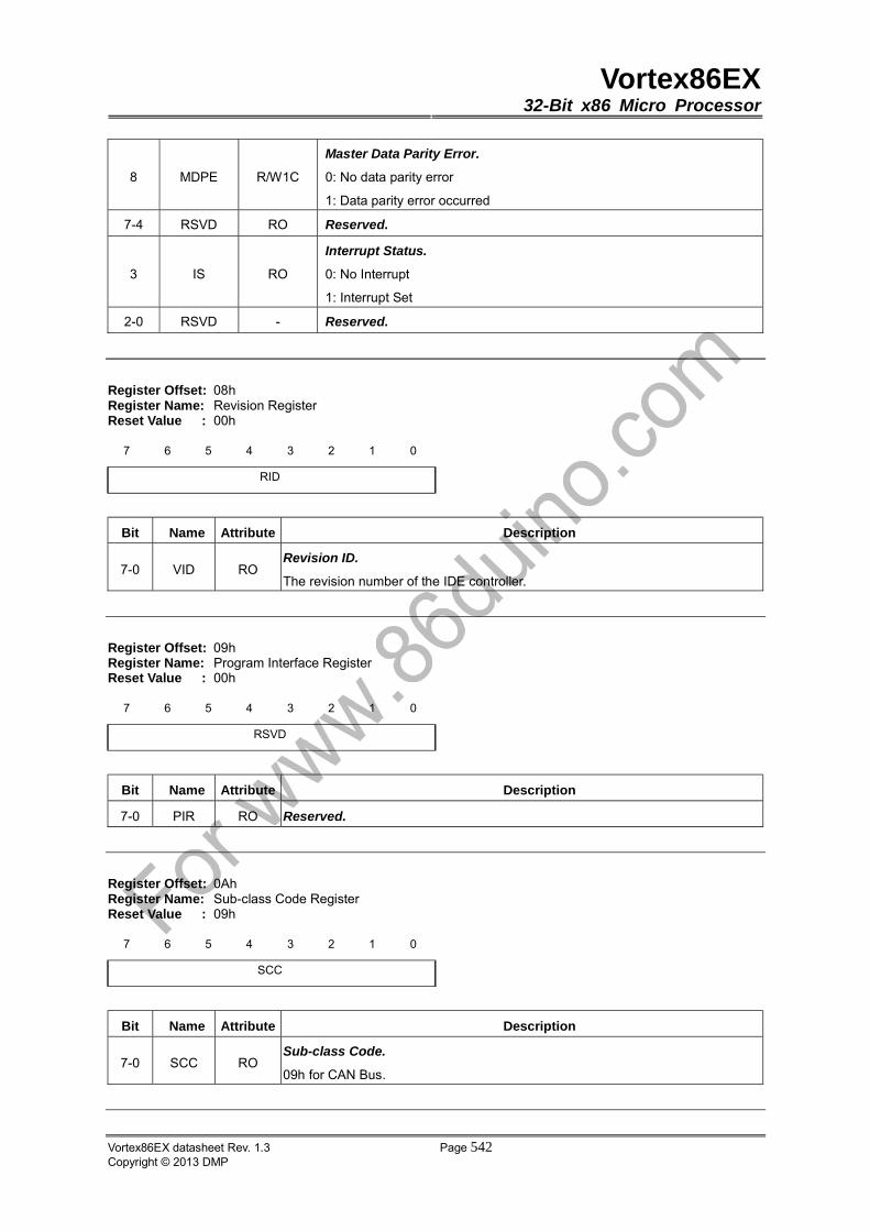
Vortex86EX32-Bit x86 Micro Processor
Vortex86EX datasheet Rev. 1.3 Page 542Copyright © 2013 DMP
8 MDPE R/W1C
Master Data Parity Error.
0: No data parity error
1: Data parity error occurred
7-4 RSVD RO Reserved.
3 IS RO
Interrupt Status.
0: No Interrupt
1: Interrupt Set
2-0 RSVD - Reserved.
Register Offset: 08h Register Name: Revision Register Reset Value : 00h
7 6 5 4 3 2 1 0
RID
Bit Name Attribute Description
7-0 VID RO Revision ID.
The revision number of the IDE controller.
Register Offset: 09h Register Name: Program Interface Register Reset Value : 00h
7 6 5 4 3 2 1 0
RSVD
Bit Name Attribute Description
7-0 PIR RO Reserved.
Register Offset: 0Ah Register Name: Sub-class Code Register Reset Value : 09h
7 6 5 4 3 2 1 0
SCC
Bit Name Attribute Description
7-0 SCC RO Sub-class Code.
09h for CAN Bus.
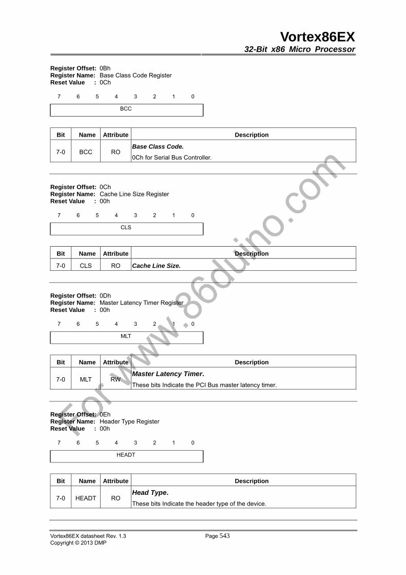
Vortex86EX32-Bit x86 Micro Processor
Vortex86EX datasheet Rev. 1.3 Page 543Copyright © 2013 DMP
Register Offset: 0Bh Register Name: Base Class Code Register Reset Value : 0Ch
7 6 5 4 3 2 1 0
BCC
Bit Name Attribute Description
7-0 BCC RO Base Class Code.
0Ch for Serial Bus Controller.
Register Offset: 0Ch Register Name: Cache Line Size Register Reset Value : 00h
7 6 5 4 3 2 1 0
CLS
Bit Name Attribute Description
7-0 CLS RO Cache Line Size.
Register Offset: 0Dh Register Name: Master Latency Timer Register Reset Value : 00h
7 6 5 4 3 2 1 0
MLT
Bit Name Attribute Description
7-0 MLT RW Master Latency Timer.
These bits Indicate the PCI Bus master latency timer.
Register Offset: 0Eh Register Name: Header Type Register Reset Value : 00h
7 6 5 4 3 2 1 0
HEADT
Bit Name Attribute Description
7-0 HEADT RO Head Type.
These bits Indicate the header type of the device.
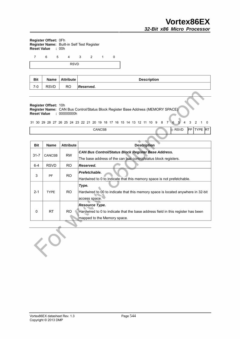
Vortex86EX32-Bit x86 Micro Processor
Vortex86EX datasheet Rev. 1.3 Page 544Copyright © 2013 DMP
Register Offset: 0Fh Register Name: Built-in Self Test Register Reset Value : 00h
7 6 5 4 3 2 1 0
RSVD
Bit Name Attribute Description
7-0 RSVD RO Reserved.
Register Offset: 10h Register Name: CAN Bus Control/Status Block Register Base Address (MEMORY SPACE) Reset Value : 00000000h
31 30 29 28 27 26 25 24 23 22 21 20 19 18 17 16 15 14 13 12 11 10 9 8 7 6 5 4 3 2 1 0
CANCSB RSVD PF TYPE RT
Bit Name Attribute Description
31-7 CANCSB RW CAN Bus Control/Status Block Register Base Address.
The base address of the can bus control/status block registers.
6-4 RSVD RO Reserved.
3 PF RO Prefetchable.
Hardwired to 0 to indicate that this memory space is not prefetchable.
2-1 TYPE RO
Type.
Hardwired to 00 to indicate that this memory space is located anywhere in 32-bit
access space.
0 RT RO
Resource Type.
Hardwired to 0 to indicate that the base address field in this register has been
mapped to the Memory space.
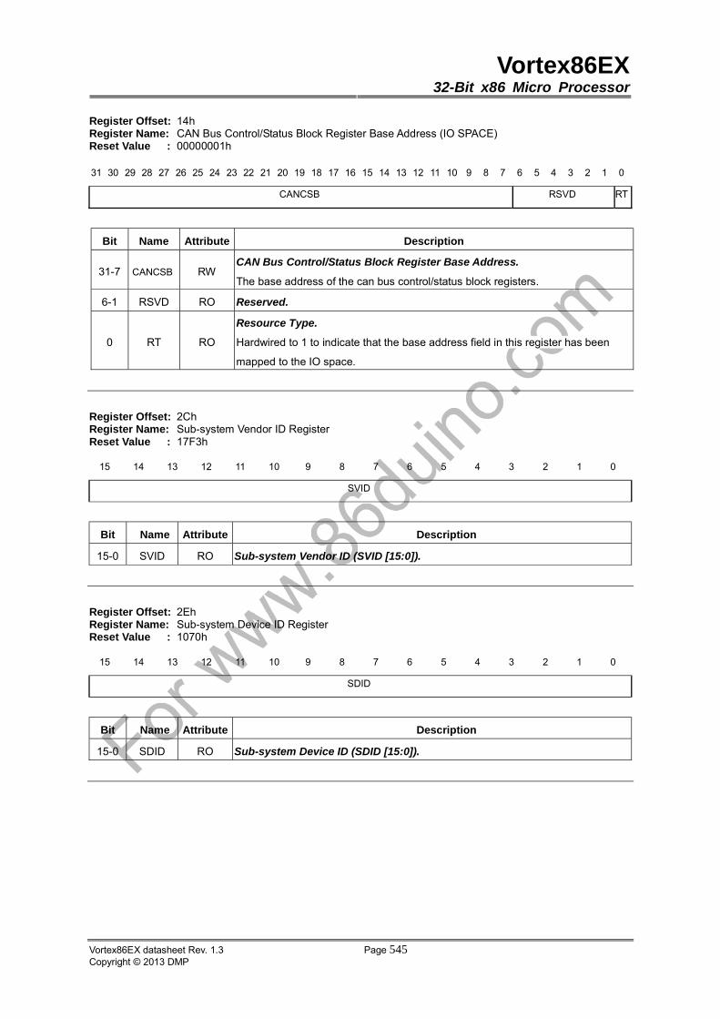
Vortex86EX32-Bit x86 Micro Processor
Vortex86EX datasheet Rev. 1.3 Page 545Copyright © 2013 DMP
Register Offset: 14h Register Name: CAN Bus Control/Status Block Register Base Address (IO SPACE) Reset Value : 00000001h
31 30 29 28 27 26 25 24 23 22 21 20 19 18 17 16 15 14 13 12 11 10 9 8 7 6 5 4 3 2 1 0
CANCSB RSVD RT
Bit Name Attribute Description
31-7 CANCSB RW CAN Bus Control/Status Block Register Base Address.
The base address of the can bus control/status block registers.
6-1 RSVD RO Reserved.
0 RT RO
Resource Type.
Hardwired to 1 to indicate that the base address field in this register has been
mapped to the IO space.
Register Offset: 2Ch Register Name: Sub-system Vendor ID Register Reset Value : 17F3h
15 14 13 12 11 10 9 8 7 6 5 4 3 2 1 0
SVID
Bit Name Attribute Description
15-0 SVID RO Sub-system Vendor ID (SVID [15:0]).
Register Offset: 2Eh Register Name: Sub-system Device ID Register Reset Value : 1070h
15 14 13 12 11 10 9 8 7 6 5 4 3 2 1 0
SDID
Bit Name Attribute Description
15-0 SDID RO Sub-system Device ID (SDID [15:0]).
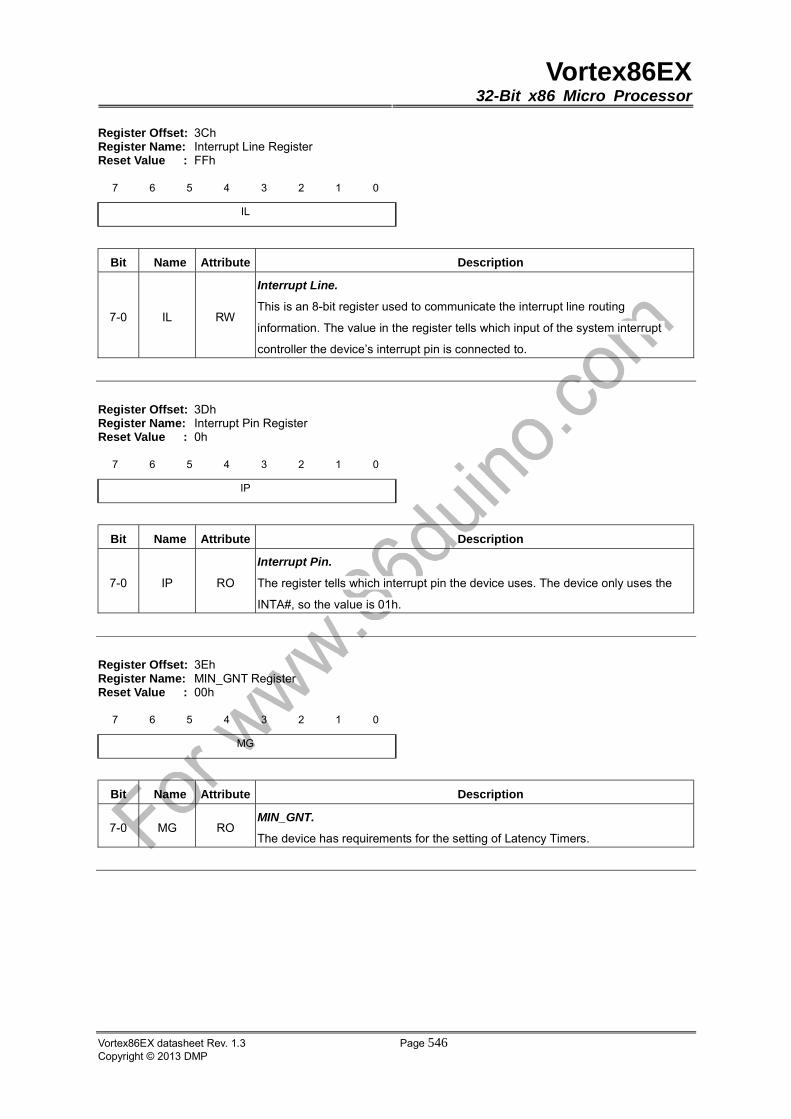
Vortex86EX32-Bit x86 Micro Processor
Vortex86EX datasheet Rev. 1.3 Page 546Copyright © 2013 DMP
Register Offset: 3Ch Register Name: Interrupt Line Register Reset Value : FFh
7 6 5 4 3 2 1 0
IL
Bit Name Attribute Description
7-0 IL RW
Interrupt Line.
This is an 8-bit register used to communicate the interrupt line routing
information. The value in the register tells which input of the system interrupt
controller the device’s interrupt pin is connected to.
Register Offset: 3Dh Register Name: Interrupt Pin Register Reset Value : 0h
7 6 5 4 3 2 1 0
IP
Bit Name Attribute Description
7-0 IP RO
Interrupt Pin.
The register tells which interrupt pin the device uses. The device only uses the
INTA#, so the value is 01h.
Register Offset: 3Eh Register Name: MIN_GNT Register Reset Value : 00h
7 6 5 4 3 2 1 0
MG
Bit Name Attribute Description
7-0 MG RO MIN_GNT.
The device has requirements for the setting of Latency Timers.
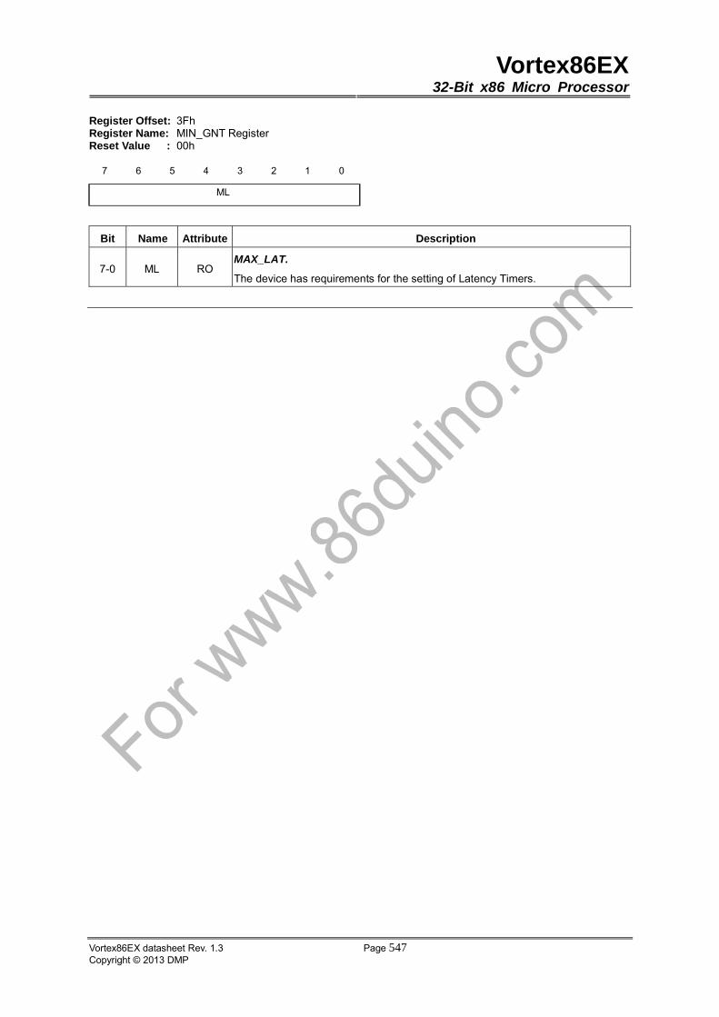
Vortex86EX32-Bit x86 Micro Processor
Vortex86EX datasheet Rev. 1.3 Page 547Copyright © 2013 DMP
Register Offset: 3Fh Register Name: MIN_GNT Register Reset Value : 00h
7 6 5 4 3 2 1 0
ML
Bit Name Attribute Description
7-0 ML RO MAX_LAT.
The device has requirements for the setting of Latency Timers.
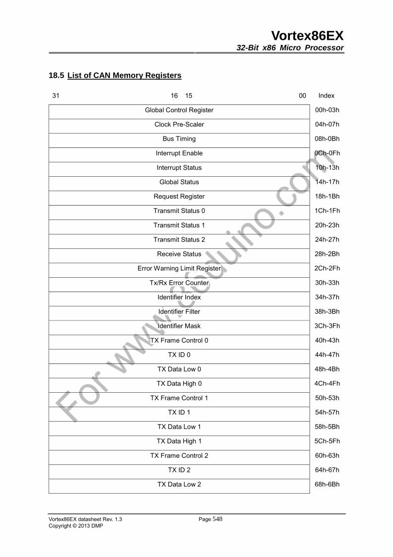
Vortex86EX32-Bit x86 Micro Processor
Vortex86EX datasheet Rev. 1.3 Page 548Copyright © 2013 DMP
18.5 List of CAN Memory Registers
31 16 15 00 Index
Global Control Register 00h-03h
Clock Pre-Scaler 04h-07h
Bus Timing 08h-0Bh
Interrupt Enable 0Ch-0Fh
Interrupt Status 10h-13h
Global Status 14h-17h
Request Register 18h-1Bh
Transmit Status 0 1Ch-1Fh
Transmit Status 1 20h-23h
Transmit Status 2 24h-27h
Receive Status 28h-2Bh
Error Warning Limit Register 2Ch-2Fh
Tx/Rx Error Counter 30h-33h
Identifier Index 34h-37h
Identifier Filter 38h-3Bh
Identifier Mask 3Ch-3Fh
TX Frame Control 0 40h-43h
TX ID 0 44h-47h
TX Data Low 0 48h-4Bh
TX Data High 0 4Ch-4Fh
TX Frame Control 1 50h-53h
TX ID 1 54h-57h
TX Data Low 1 58h-5Bh
TX Data High 1 5Ch-5Fh
TX Frame Control 2 60h-63h
TX ID 2 64h-67h
TX Data Low 2 68h-6Bh
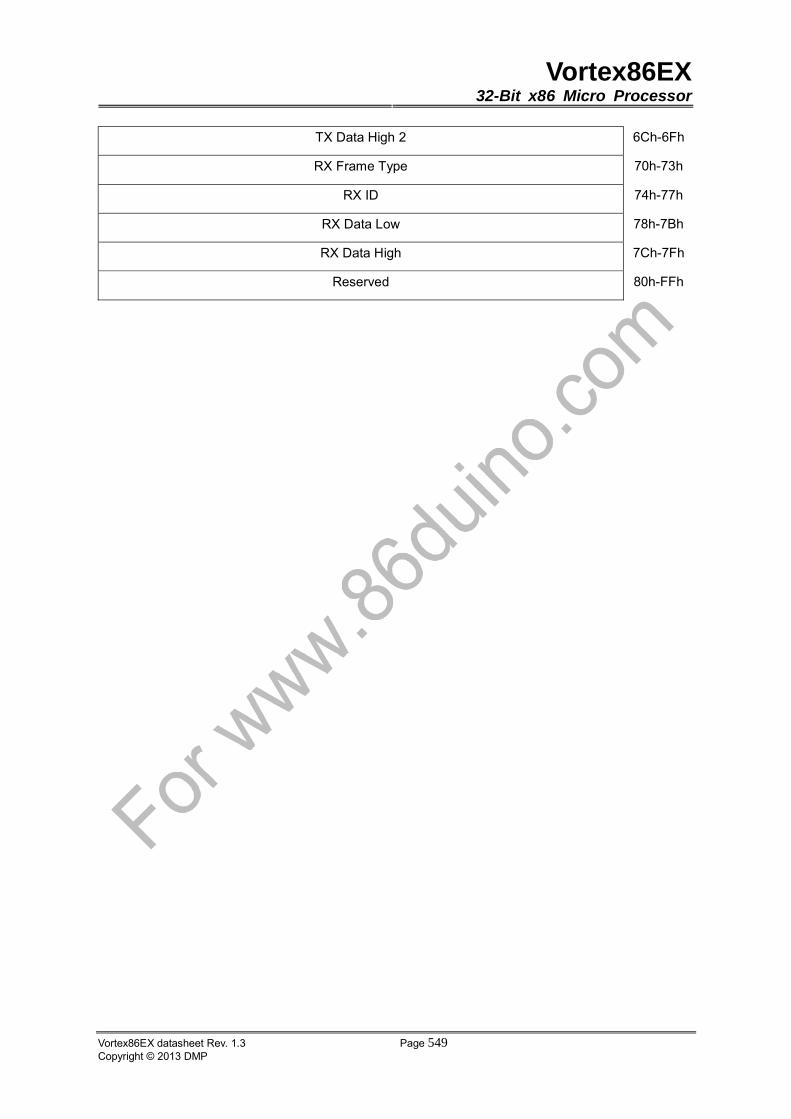
Vortex86EX32-Bit x86 Micro Processor
Vortex86EX datasheet Rev. 1.3 Page 549Copyright © 2013 DMP
TX Data High 2 6Ch-6Fh
RX Frame Type 70h-73h
RX ID 74h-77h
RX Data Low 78h-7Bh
RX Data High 7Ch-7Fh
Reserved 80h-FFh
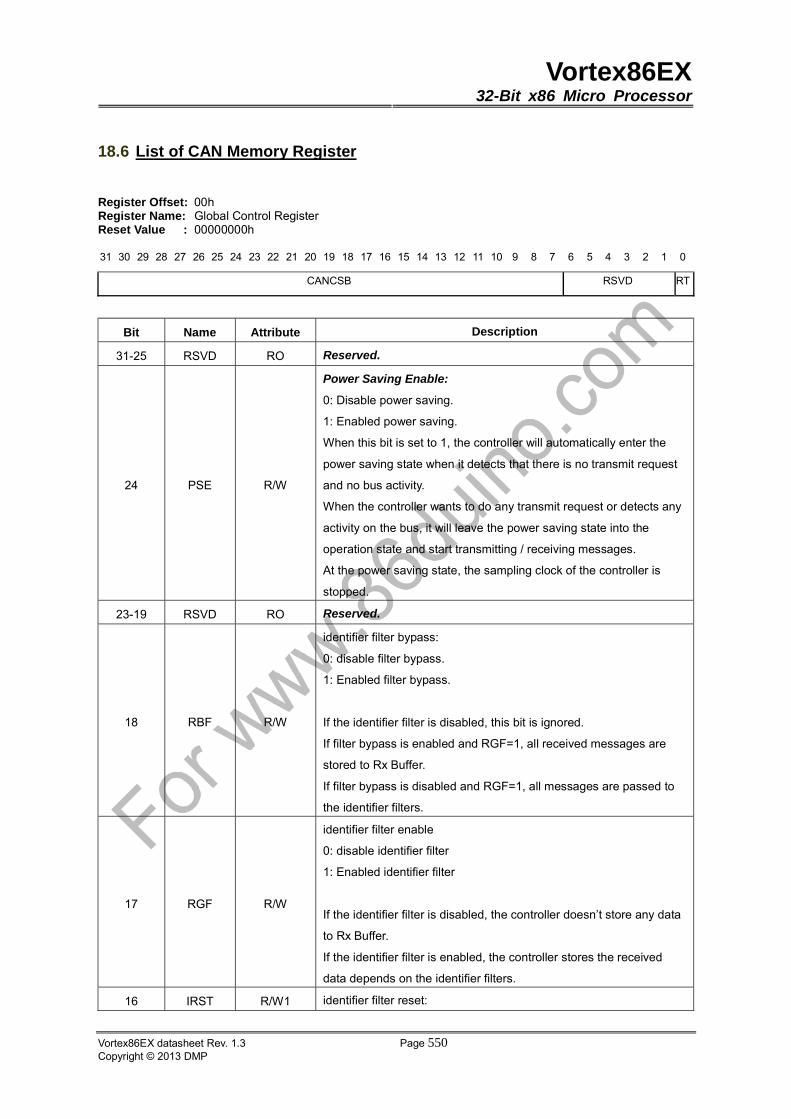
Vortex86EX32-Bit x86 Micro Processor
Vortex86EX datasheet Rev. 1.3 Page 550Copyright © 2013 DMP
18.6 List of CAN Memory Register
Register Offset: 00h Register Name: Global Control Register Reset Value : 00000000h
31 30 29 28 27 26 25 24 23 22 21 20 19 18 17 16 15 14 13 12 11 10 9 8 7 6 5 4 3 2 1 0
CANCSB RSVD RT
Bit Name Attribute Description
31-25 RSVD RO Reserved.
24 PSE R/W
Power Saving Enable:
0: Disable power saving.
1: Enabled power saving.
When this bit is set to 1, the controller will automatically enter the
power saving state when it detects that there is no transmit request
and no bus activity.
When the controller wants to do any transmit request or detects any
activity on the bus, it will leave the power saving state into the
operation state and start transmitting / receiving messages.
At the power saving state, the sampling clock of the controller is
stopped.
23-19 RSVD RO Reserved.
18 RBF R/W
identifier filter bypass:
0: disable filter bypass.
1: Enabled filter bypass.
If the identifier filter is disabled, this bit is ignored.
If filter bypass is enabled and RGF=1, all received messages are
stored to Rx Buffer.
If filter bypass is disabled and RGF=1, all messages are passed to
the identifier filters.
17 RGF R/W
identifier filter enable
0: disable identifier filter
1: Enabled identifier filter
If the identifier filter is disabled, the controller doesn’t store any data
to Rx Buffer.
If the identifier filter is enabled, the controller stores the received
data depends on the identifier filters.
16 IRST R/W1 identifier filter reset:
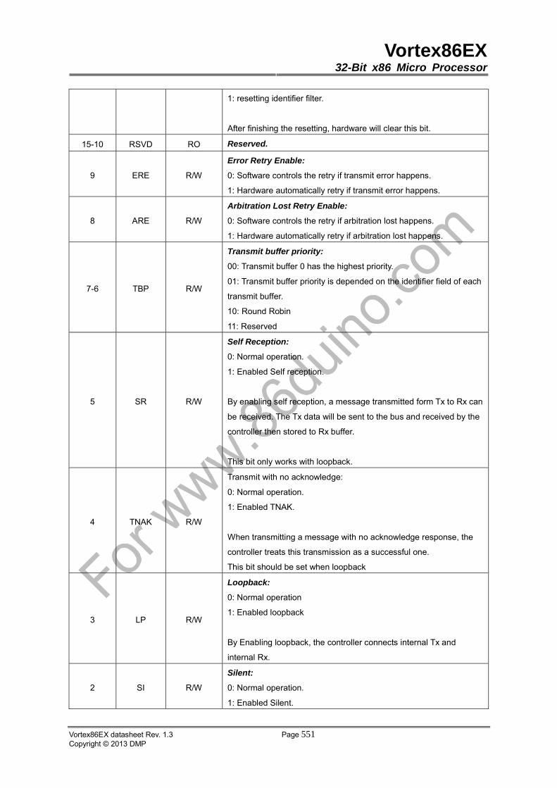
Vortex86EX32-Bit x86 Micro Processor
Vortex86EX datasheet Rev. 1.3 Page 551Copyright © 2013 DMP
1: resetting identifier filter.
After finishing the resetting, hardware will clear this bit.
15-10 RSVD RO Reserved.
9 ERE R/W
Error Retry Enable:
0: Software controls the retry if transmit error happens.
1: Hardware automatically retry if transmit error happens.
8 ARE R/W
Arbitration Lost Retry Enable:
0: Software controls the retry if arbitration lost happens.
1: Hardware automatically retry if arbitration lost happens.
7-6 TBP R/W
Transmit buffer priority:
00: Transmit buffer 0 has the highest priority.
01: Transmit buffer priority is depended on the identifier field of each
transmit buffer.
10: Round Robin
11: Reserved
5 SR R/W
Self Reception:
0: Normal operation.
1: Enabled Self reception.
By enabling self reception, a message transmitted form Tx to Rx can
be received. The Tx data will be sent to the bus and received by the
controller then stored to Rx buffer.
This bit only works with loopback.
4 TNAK R/W
Transmit with no acknowledge:
0: Normal operation.
1: Enabled TNAK.
When transmitting a message with no acknowledge response, the
controller treats this transmission as a successful one.
This bit should be set when loopback
3 LP R/W
Loopback:
0: Normal operation
1: Enabled loopback
By Enabling loopback, the controller connects internal Tx and
internal Rx.
2 SI R/W
Silent:
0: Normal operation.
1: Enabled Silent.
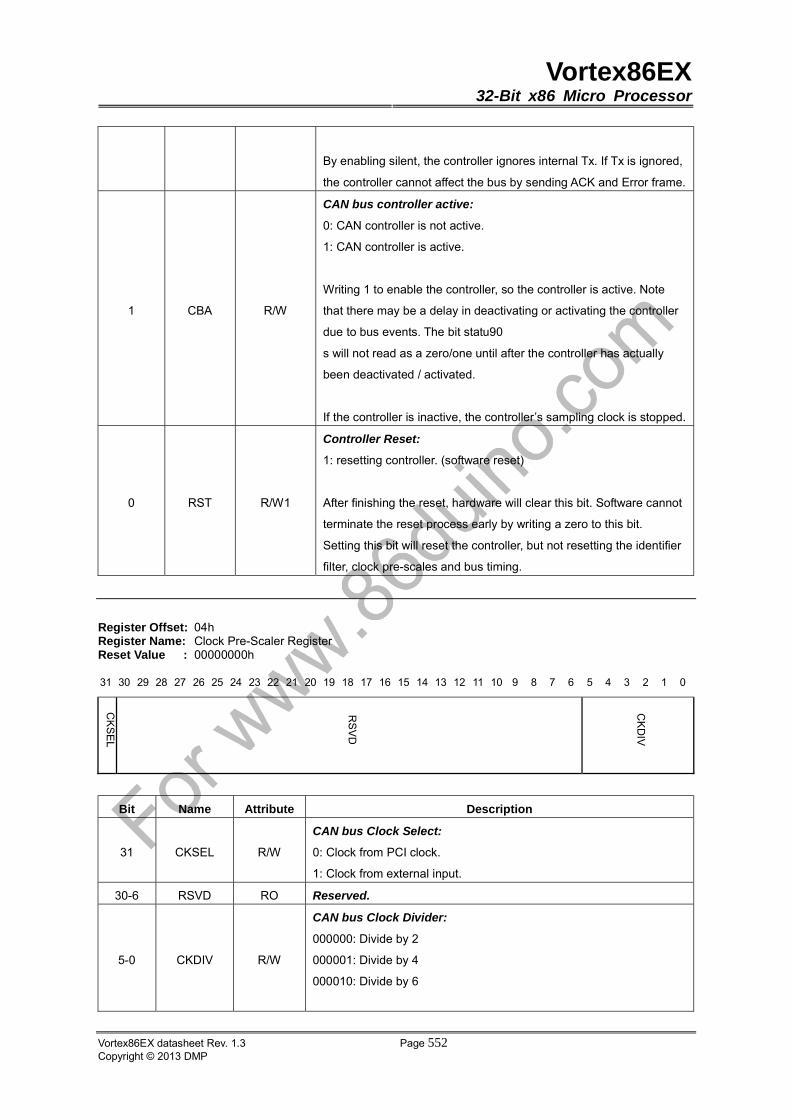
Vortex86EX32-Bit x86 Micro Processor
Vortex86EX datasheet Rev. 1.3 Page 552Copyright © 2013 DMP
By enabling silent, the controller ignores internal Tx. If Tx is ignored,
the controller cannot affect the bus by sending ACK and Error frame.
1 CBA R/W
CAN bus controller active:
0: CAN controller is not active.
1: CAN controller is active.
Writing 1 to enable the controller, so the controller is active. Note
that there may be a delay in deactivating or activating the controller
due to bus events. The bit statu90
s will not read as a zero/one until after the controller has actually
been deactivated / activated.
If the controller is inactive, the controller’s sampling clock is stopped.
0 RST R/W1
Controller Reset:
1: resetting controller. (software reset)
After finishing the reset, hardware will clear this bit. Software cannot
terminate the reset process early by writing a zero to this bit.
Setting this bit will reset the controller, but not resetting the identifier
filter, clock pre-scales and bus timing.
Register Offset: 04h Register Name: Clock Pre-Scaler Register Reset Value : 00000000h
31 30 29 28 27 26 25 24 23 22 21 20 19 18 17 16 15 14 13 12 11 10 9 8 7 6 5 4 3 2 1 0
Bit Name Attribute Description
31 CKSEL R/W
CAN bus Clock Select:
0: Clock from PCI clock.
1: Clock from external input.
30-6 RSVD RO Reserved.
5-0 CKDIV R/W
CAN bus Clock Divider:
000000: Divide by 2
000001: Divide by 4
000010: Divide by 6
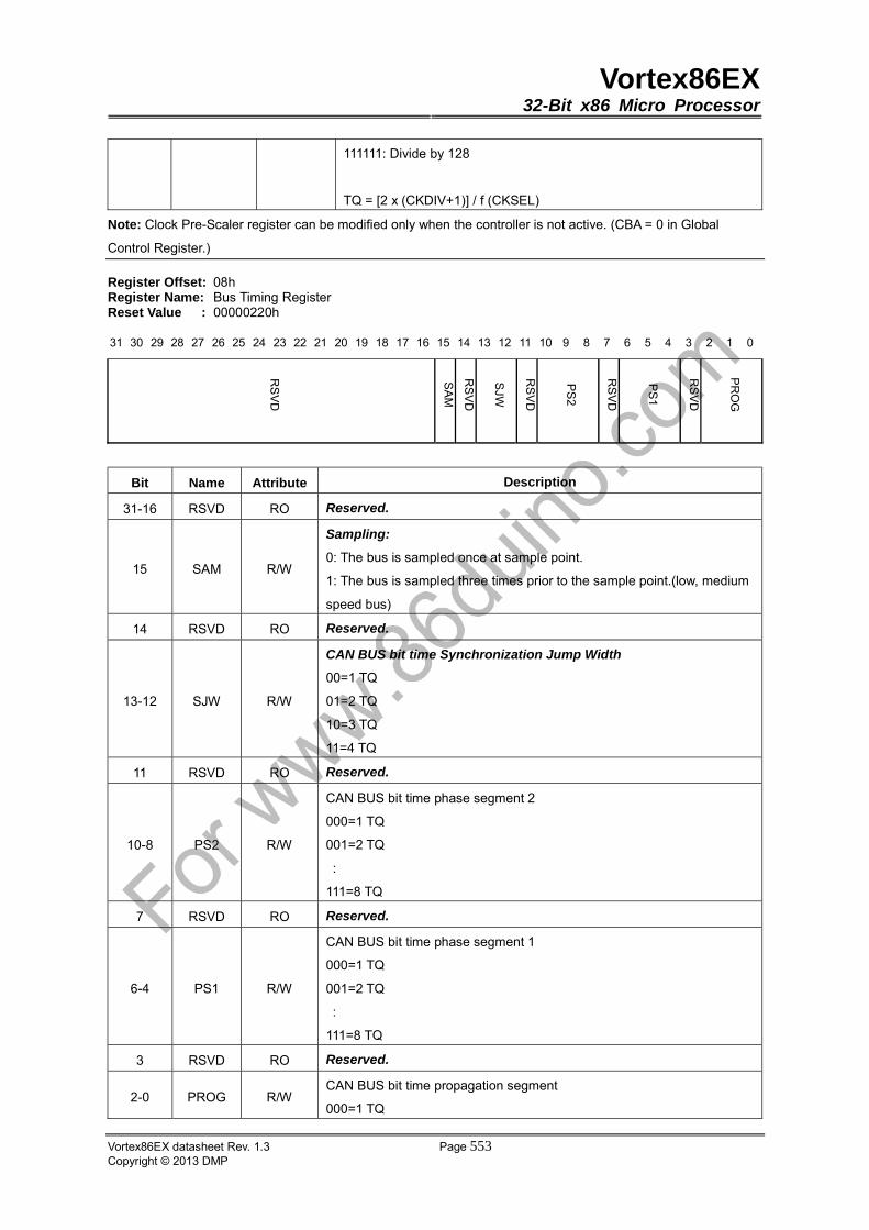
Vortex86EX32-Bit x86 Micro Processor
Vortex86EX datasheet Rev. 1.3 Page 553Copyright © 2013 DMP
111111: Divide by 128
TQ = [2 x (CKDIV+1)] / f (CKSEL)
Note: Clock Pre-Scaler register can be modified only when the controller is not active. (CBA = 0 in Global
Control Register.)
Register Offset: 08h Register Name: Bus Timing Register Reset Value : 00000220h
31 30 29 28 27 26 25 24 23 22 21 20 19 18 17 16 15 14 13 12 11 10 9 8 7 6 5 4 3 2 1 0
Bit Name Attribute Description
31-16 RSVD RO Reserved.
15 SAM R/W
Sampling:
0: The bus is sampled once at sample point.
1: The bus is sampled three times prior to the sample point.(low, medium
speed bus)
14 RSVD RO Reserved.
13-12 SJW R/W
CAN BUS bit time Synchronization Jump Width
00=1 TQ
01=2 TQ
10=3 TQ
11=4 TQ
11 RSVD RO Reserved.
10-8 PS2 R/W
CAN BUS bit time phase segment 2
000=1 TQ
001=2 TQ
:
111=8 TQ
7 RSVD RO Reserved.
6-4 PS1 R/W
CAN BUS bit time phase segment 1
000=1 TQ
001=2 TQ
:
111=8 TQ
3 RSVD RO Reserved.
2-0 PROG R/W CAN BUS bit time propagation segment
000=1 TQ

Vortex86EX32-Bit x86 Micro Processor
Vortex86EX datasheet Rev. 1.3 Page 554Copyright © 2013 DMP
001=2 TQ
:
111=8 TQ
Note: Bus Timing Register can be modified only when the controller is not active. (CBA = 0 in Global Control
Register.)
Register Offset: 0Ch Register Name: Interrupt Enable Register Reset Value : 00000000h
31 30 29 28 27 26 25 24 23 22 21 20 19 18 17 16 15 14 13 12 11 10 9 8 7 6 5 4 3 2 1 0
Bit Name R/W Description
31-11 RSVD RO Reserved.
10 XPIE R/W Exit power saving interrupt enable.
9 RBOIE R/W Receive buffer overrun interrupt enable.
8 RBEIE R/W Receive bus error interrupt enable.
7 ALIE R/W Arbitration lost interrupt enable.
6 BOIE R/W Bus Off interrupt enable.
5 EPIE R/W Error passive interrupt enable.
4 ECIE R/W Error counter warning interrupt enable.
3 TX2IE R/W TxBuffer2 transmit request interrupt enable.
2 TX1IE R/W TxBuffer1 transmit request interrupt enable.
1 TX0IE R/W TxBuffer0 transmit request interrupt enable.
0 RXIE R/W Receive interrupt enable:
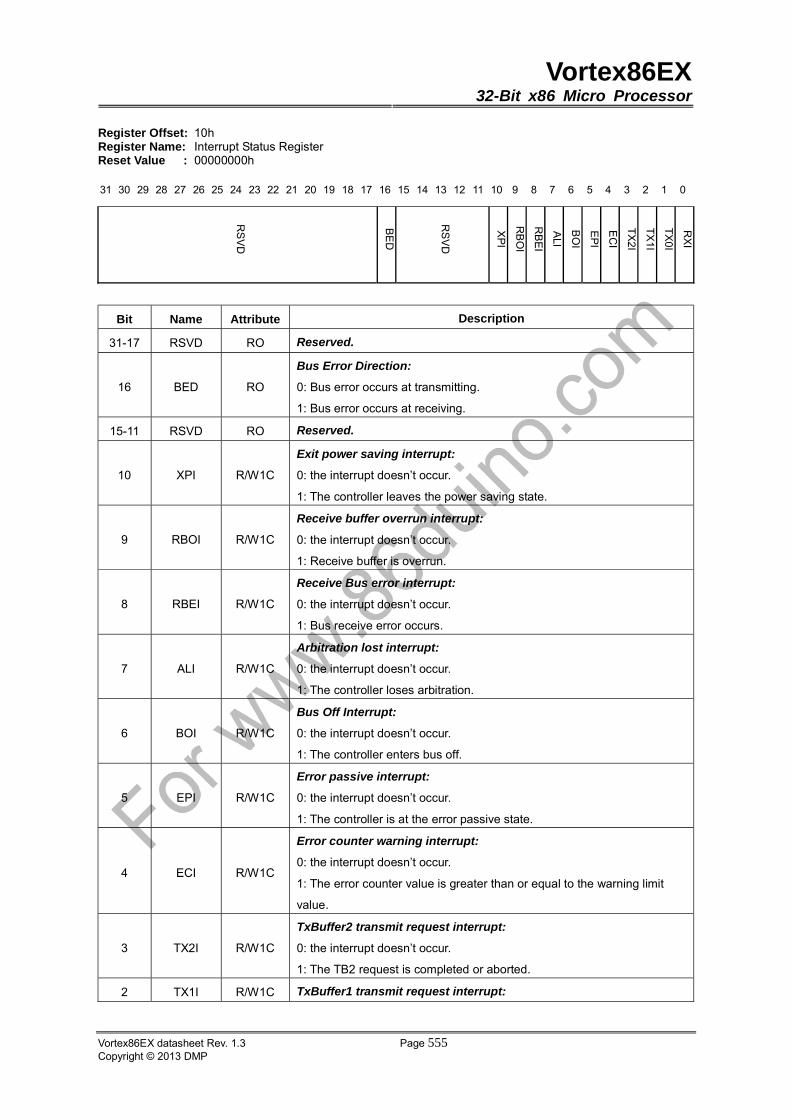
Vortex86EX32-Bit x86 Micro Processor
Vortex86EX datasheet Rev. 1.3 Page 555Copyright © 2013 DMP
Register Offset: 10h Register Name: Interrupt Status Register Reset Value : 00000000h
31 30 29 28 27 26 25 24 23 22 21 20 19 18 17 16 15 14 13 12 11 10 9 8 7 6 5 4 3 2 1 0
Bit Name Attribute Description
31-17 RSVD RO Reserved.
16 BED RO
Bus Error Direction:
0: Bus error occurs at transmitting.
1: Bus error occurs at receiving.
15-11 RSVD RO Reserved.
10 XPI R/W1C
Exit power saving interrupt:
0: the interrupt doesn’t occur.
1: The controller leaves the power saving state.
9 RBOI R/W1C
Receive buffer overrun interrupt:
0: the interrupt doesn’t occur.
1: Receive buffer is overrun.
8 RBEI R/W1C
Receive Bus error interrupt:
0: the interrupt doesn’t occur.
1: Bus receive error occurs.
7 ALI R/W1C
Arbitration lost interrupt:
0: the interrupt doesn’t occur.
1: The controller loses arbitration.
6 BOI R/W1C
Bus Off Interrupt:
0: the interrupt doesn’t occur.
1: The controller enters bus off.
5 EPI R/W1C
Error passive interrupt:
0: the interrupt doesn’t occur.
1: The controller is at the error passive state.
4 ECI R/W1C
Error counter warning interrupt:
0: the interrupt doesn’t occur.
1: The error counter value is greater than or equal to the warning limit
value.
3 TX2I R/W1C
TxBuffer2 transmit request interrupt:
0: the interrupt doesn’t occur.
1: The TB2 request is completed or aborted.
2 TX1I R/W1C TxBuffer1 transmit request interrupt:
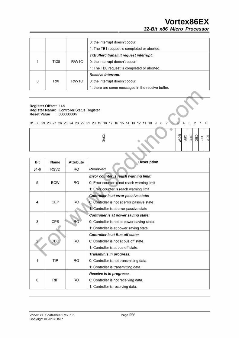
Vortex86EX32-Bit x86 Micro Processor
Vortex86EX datasheet Rev. 1.3 Page 556Copyright © 2013 DMP
0: the interrupt doesn’t occur.
1: The TB1 request is completed or aborted.
1 TX0I R/W1C
TxBuffer0 transmit request interrupt:
0: the interrupt doesn’t occur.
1: The TB0 request is completed or aborted.
0 RXI R/W1C
Receive interrupt:
0: the interrupt doesn’t occur.
1: there are some messages in the receive buffer.
Register Offset: 14h Register Name: Controller Status RegisterReset Value : 00000000h
31 30 29 28 27 26 25 24 23 22 21 20 19 18 17 16 15 14 13 12 11 10 9 8 7 6 5 4 3 2 1 0
Bit Name Attribute Description
31-6 RSVD RO Reserved.
5 ECW RO
Error counter is reach warning limit:
0: Error counter is not reach warning limit
1: Error counter is reach warning limit
4 CEP RO
Controller is at error passive state:
0: Controller is not at error passive state
1: Controller is at error passive state
3 CPS RO
Controller is at power saving state:
0: Controller is not at power saving state.
1: Controller is at power saving state.
2 CBO RO
Controller is at Bus off state:
0: Controller is not at bus off state.
1: Controller is at bus off state.
1 TIP RO
Transmit is in progress:
0: Controller is not transmitting data.
1: Controller is transmitting data.
0 RIP RO
Receive is in progress:
0: Controller is not receiving data.
1: Controller is receiving data.
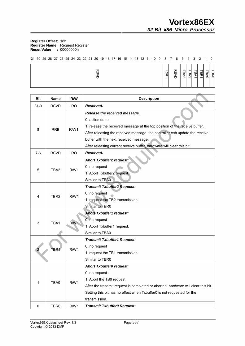
Vortex86EX32-Bit x86 Micro Processor
Vortex86EX datasheet Rev. 1.3 Page 557Copyright © 2013 DMP
Register Offset: 18h Register Name: Request Register Reset Value : 00000000h
31 30 29 28 27 26 25 24 23 22 21 20 19 18 17 16 15 14 13 12 11 10 9 8 7 6 5 4 3 2 1 0
Bit Name R/W Description
31-9 RSVD RO Reserved.
8 RRB R/W1
Release the received message.
0: action done
1: release the received message at the top position of the receive buffer.
After releasing the received message, the controller can update the receive
buffer with the next received message.
After releasing current receive buffer, hardware will clear this bit.
7-6 RSVD RO Reserved.
5 TBA2 R/W1
Abort Txbuffer2 request:
0: no request
1: Abort Txbuffer2 request.
Similar to TBA0
4 TBR2 R/W1
Transmit Txbuffer2 Request:
0: no request
1: request the TB2 transmission.
Similar to TBR0
3 TBA1 R/W1
Abort Txbuffer1 request:
0: no request
1: Abort Txbuffer1 request.
Similar to TBA0
2 TBR1 R/W1
Transmit Txbuffer1 Request:
0: no request
1: request the TB1 transmission.
Similar to TBR0
1 TBA0 R/W1
Abort Txbuffer0 request:
0: no request
1: Abort the TB0 request.
After the transmit request is completed or aborted, hardware will clear this bit.
Setting this bit has no effect when Txbuffer0 is not requested for the
transmission.
0 TBR0 R/W1 Transmit Txbuffer0 Request:
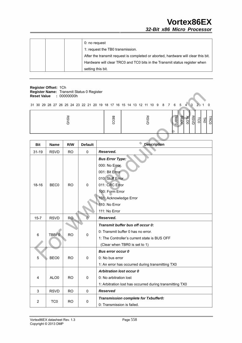
Vortex86EX32-Bit x86 Micro Processor
Vortex86EX datasheet Rev. 1.3 Page 558Copyright © 2013 DMP
0: no request
1: request the TB0 transmission.
After the transmit request is completed or aborted, hardware will clear this bit.
Hardware will clear TRC0 and TC0 bits in the Transmit status register when
setting this bit.
Register Offset: 1Ch Register Name: Transmit Status 0 Register Reset Value : 00000000h
31 30 29 28 27 26 25 24 23 22 21 20 19 18 17 16 15 14 13 12 11 10 9 8 7 6 5 4 3 2 1 0
Bit Name R/W Default Description
31-19 RSVD RO 0 Reserved.
18-16 BEC0 RO 0
Bus Error Type:
000: No Error
001: Bit Error
010: Stuff Error
011: CRC Error
100: Form Error
101: Acknowledge Error
110: No Error
111: No Error
15-7 RSVD RO 0 Reserved.
6 TBBF0 RO 0
Transmit buffer bus off occur 0:
0: Transmit buffer 0 has no error.
1: The Controller’s current state is BUS OFF
(Clear when TBR0 is set to 1)
5 BEO0 RO 0
Bus error occur 0
0: No bus error
1: An error has occurred during transmitting TX0
4 ALO0 RO 0
Arbitration lost occur 0
0: No arbitration lost
1: Arbitration lost has occurred during transmitting TX0
3 RSVD RO 0 Reserved
2 TC0 RO 0 Transmission complete for Txbuffer0:
0: Transmission is failed.
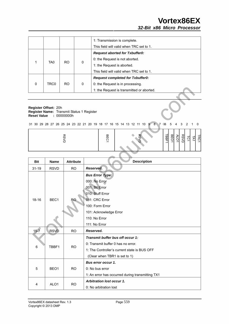
Vortex86EX32-Bit x86 Micro Processor
Vortex86EX datasheet Rev. 1.3 Page 559Copyright © 2013 DMP
1: Transmission is complete.
This field will valid when TRC set to 1.
1 TA0 RO 0
Request aborted for Txbuffer0:
0: the Request is not aborted.
1: the Request is aborted.
This field will valid when TRC set to 1.
0 TRC0 RO 0
Request completed for Txbuffer0:
0: the Request is in processing.
1: the Request is transmitted or aborted.
Register Offset: 20h Register Name: Transmit Status 1 Register Reset Value : 00000000h
31 30 29 28 27 26 25 24 23 22 21 20 19 18 17 16 15 14 13 12 11 10 9 8 7 6 5 4 3 2 1 0
Bit Name Attribute Description
31-19 RSVD RO Reserved.
18-16 BEC1 RO
Bus Error Type:
000: No Error
001: Bit Error
010: Stuff Error
011: CRC Error
100: Form Error
101: Acknowledge Error
110: No Error
111: No Error
15-7 RSVD RO Reserved.
6 TBBF1 RO
Transmit buffer bus off occur 1:
0: Transmit buffer 0 has no error.
1: The Controller’s current state is BUS OFF
(Clear when TBR1 is set to 1)
5 BEO1 RO
Bus error occur 1.
0: No bus error
1: An error has occurred during transmitting TX1
4 ALO1 RO Arbitration lost occur 1.
0: No arbitration lost
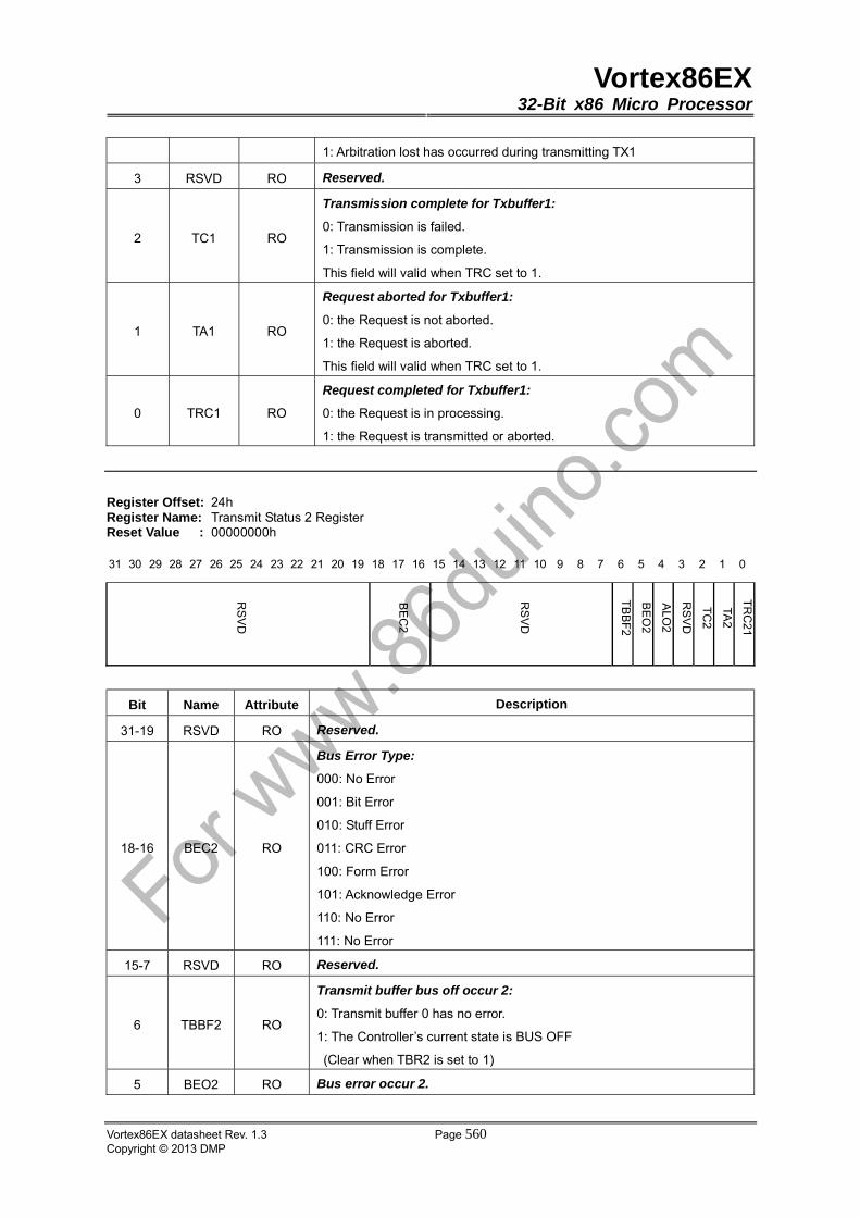
Vortex86EX32-Bit x86 Micro Processor
Vortex86EX datasheet Rev. 1.3 Page 560Copyright © 2013 DMP
1: Arbitration lost has occurred during transmitting TX1
3 RSVD RO Reserved.
2 TC1 RO
Transmission complete for Txbuffer1:
0: Transmission is failed.
1: Transmission is complete.
This field will valid when TRC set to 1.
1 TA1 RO
Request aborted for Txbuffer1:
0: the Request is not aborted.
1: the Request is aborted.
This field will valid when TRC set to 1.
0 TRC1 RO
Request completed for Txbuffer1:
0: the Request is in processing.
1: the Request is transmitted or aborted.
Register Offset: 24h Register Name: Transmit Status 2 Register Reset Value : 00000000h
31 30 29 28 27 26 25 24 23 22 21 20 19 18 17 16 15 14 13 12 11 10 9 8 7 6 5 4 3 2 1 0
Bit Name Attribute Description
31-19 RSVD RO Reserved.
18-16 BEC2 RO
Bus Error Type:
000: No Error
001: Bit Error
010: Stuff Error
011: CRC Error
100: Form Error
101: Acknowledge Error
110: No Error
111: No Error
15-7 RSVD RO Reserved.
6 TBBF2 RO
Transmit buffer bus off occur 2:
0: Transmit buffer 0 has no error.
1: The Controller’s current state is BUS OFF
(Clear when TBR2 is set to 1)
5 BEO2 RO Bus error occur 2.
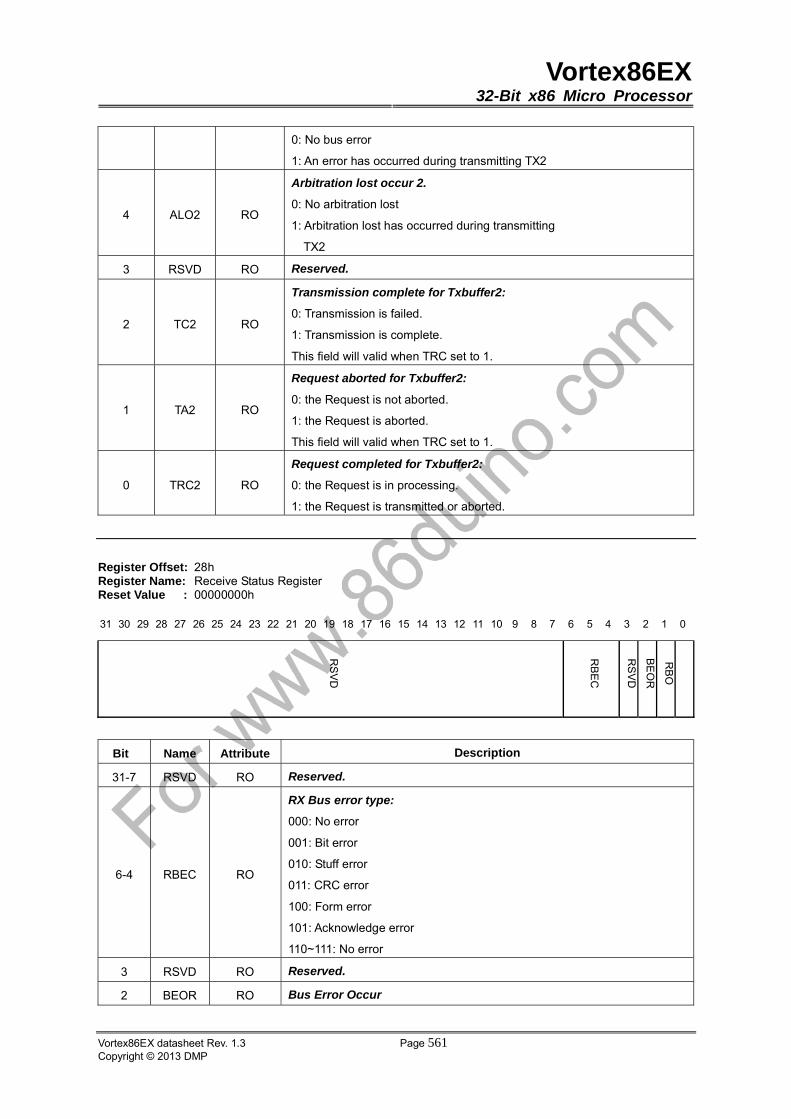
Vortex86EX32-Bit x86 Micro Processor
Vortex86EX datasheet Rev. 1.3 Page 561Copyright © 2013 DMP
0: No bus error
1: An error has occurred during transmitting TX2
4 ALO2 RO
Arbitration lost occur 2.
0: No arbitration lost
1: Arbitration lost has occurred during transmitting
TX2
3 RSVD RO Reserved.
2 TC2 RO
Transmission complete for Txbuffer2:
0: Transmission is failed.
1: Transmission is complete.
This field will valid when TRC set to 1.
1 TA2 RO
Request aborted for Txbuffer2:
0: the Request is not aborted.
1: the Request is aborted.
This field will valid when TRC set to 1.
0 TRC2 RO
Request completed for Txbuffer2:
0: the Request is in processing.
1: the Request is transmitted or aborted.
Register Offset: 28h Register Name: Receive Status Register Reset Value : 00000000h
31 30 29 28 27 26 25 24 23 22 21 20 19 18 17 16 15 14 13 12 11 10 9 8 7 6 5 4 3 2 1 0
Bit Name Attribute Description
31-7 RSVD RO Reserved.
6-4 RBEC RO
RX Bus error type:
000: No error
001: Bit error
010: Stuff error
011: CRC error
100: Form error
101: Acknowledge error
110~111: No error
3 RSVD RO Reserved.
2 BEOR RO Bus Error Occur
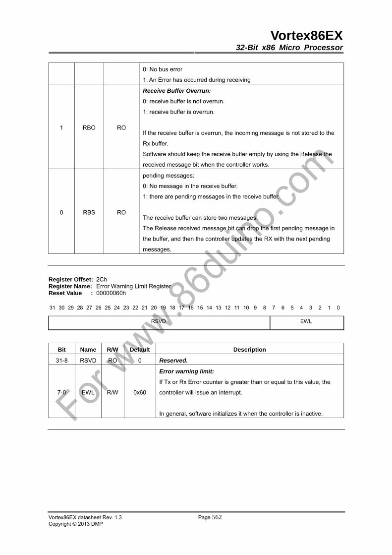
Vortex86EX32-Bit x86 Micro Processor
Vortex86EX datasheet Rev. 1.3 Page 562Copyright © 2013 DMP
0: No bus error
1: An Error has occurred during receiving
1 RBO RO
Receive Buffer Overrun:
0: receive buffer is not overrun.
1: receive buffer is overrun.
If the receive buffer is overrun, the incoming message is not stored to the
Rx buffer.
Software should keep the receive buffer empty by using the Release the
received message bit when the controller works.
0 RBS RO
pending messages:
0: No message in the receive buffer.
1: there are pending messages in the receive buffer.
The receive buffer can store two messages.
The Release received message bit can drop the first pending message in
the buffer, and then the controller updates the RX with the next pending
messages.
Register Offset: 2Ch Register Name: Error Warning Limit Register Reset Value : 00000060h
31 30 29 28 27 26 25 24 23 22 21 20 19 18 17 16 15 14 13 12 11 10 9 8 7 6 5 4 3 2 1 0
RSVD EWL
Bit Name R/W Default Description
31-8 RSVD RO 0 Reserved.
7-0 EWL R/W 0x60
Error warning limit:
If Tx or Rx Error counter is greater than or equal to this value, the
controller will issue an interrupt.
In general, software initializes it when the controller is inactive.

Vortex86EX32-Bit x86 Micro Processor
Vortex86EX datasheet Rev. 1.3 Page 563Copyright © 2013 DMP
Register Offset: 30h Register Name: Tx/Rx Error Counter Register Reset Value : 00000000h
31 30 29 28 27 26 25 24 23 22 21 20 19 18 17 16 15 14 13 12 11 10 9 8 7 6 5 4 3 2 1 0
RSVD REC RSVD TEC
Bit Name Attibute Description
31-24 RSVD RO Reserved.
23-16 REC R/W Receive Error Counter:
In general, software initializes it when the controller is active.
15-9 RSVD RO Reserved.
8-0 TEC R/W Transmit Error Counter:
In general, software initializes it when the controller is active.
Register Offset: 34h Register Name: Identifier Index Register Reset Value : 00000000h
31 30 29 28 27 26 25 24 23 22 21 20 19 18 17 16 15 14 13 12 11 10 9 8 7 6 5 4 3 2 1 0
RSVD IFU RSVD IFI
Bit Name Attribute Description
31-9 RSVD RO Reserved.
8 IFU R/W1
Identifier Filter Update.
After updating the internal filter buffer specified by filter index, hardware
will clear this bit.
7-5 RSVD RO Reserved.
4-0 IFI R/W
Identifier Filter Index:
Identifier filter index value from 0x0 ~ 0x1F
Before access to any filter through identifier filter reg and mask reg,
software should specify filter index number.

Vortex86EX32-Bit x86 Micro Processor
Vortex86EX datasheet Rev. 1.3 Page 564Copyright © 2013 DMP
Register Offset: 38h Register Name: Identifier Filter Register Reset Value : 00000000h
31 30 29 28 27 26 25 24 23 22 21 20 19 18 17 16 15 14 13 12 11 10 9 8 7 6 5 4 3 2 1 0
Bit Name R/W Default Description
31 IFE R/W 0
Identifier Filter Enable:
0: Disable ID filter.
1: Enabled ID filter.
30 IFM R/W 0
Identifier Filter Format:
0: This filter is for standard ID (11 bit ID).
1: This filter is for extended ID (29 bit ID).
29 RSVD RO 0 Reserved.
28-0 IFB R/W 0 Identifier Filter bit:
If IFM is set to 0, bit11~28 will be ignored.
Register Offset: 3Ch Register Name: Identifier Mask Register Reset Value : 00000000h
31 30 29 28 27 26 25 24 23 22 21 20 19 18 17 16 15 14 13 12 11 10 9 8 7 6 5 4 3 2 1 0
Bit Name Attribute Description
31-29 RSVD RO Reserved.
28-0 IMB R/W Identifier Mask bit:
If IFM is set to 0, bit 28-11 will be ignored.
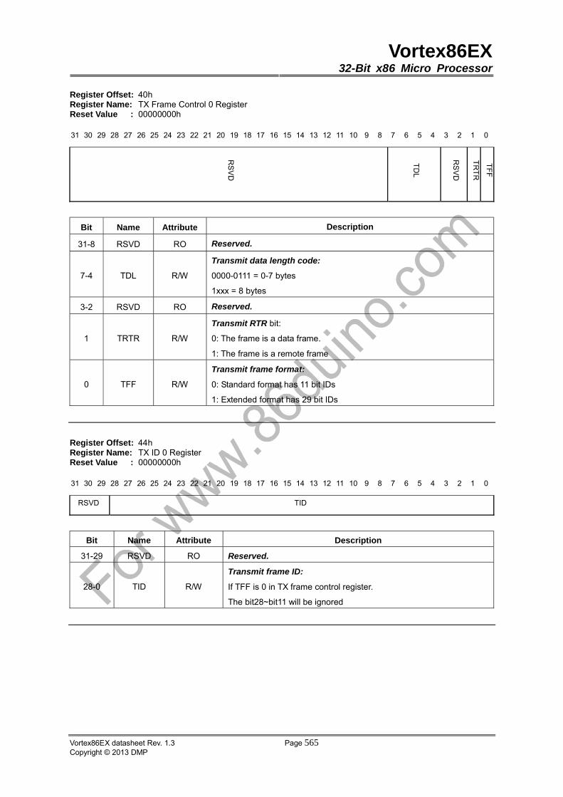
Vortex86EX32-Bit x86 Micro Processor
Vortex86EX datasheet Rev. 1.3 Page 565Copyright © 2013 DMP
Register Offset: 40h Register Name: TX Frame Control 0 Register Reset Value : 00000000h
31 30 29 28 27 26 25 24 23 22 21 20 19 18 17 16 15 14 13 12 11 10 9 8 7 6 5 4 3 2 1 0
Bit Name Attribute Description
31-8 RSVD RO Reserved.
7-4 TDL R/W
Transmit data length code:
0000-0111 = 0-7 bytes
1xxx = 8 bytes
3-2 RSVD RO Reserved.
1 TRTR R/W
Transmit RTR bit:
0: The frame is a data frame.
1: The frame is a remote frame
0 TFF R/W
Transmit frame format:
0: Standard format has 11 bit IDs
1: Extended format has 29 bit IDs
Register Offset: 44h Register Name: TX ID 0 Register Reset Value : 00000000h
31 30 29 28 27 26 25 24 23 22 21 20 19 18 17 16 15 14 13 12 11 10 9 8 7 6 5 4 3 2 1 0
RSVD TID
Bit Name Attribute Description
31-29 RSVD RO Reserved.
28-0 TID R/W
Transmit frame ID:
If TFF is 0 in TX frame control register.
The bit28~bit11 will be ignored
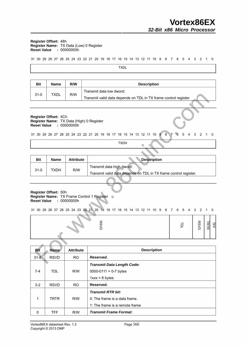
Vortex86EX32-Bit x86 Micro Processor
Vortex86EX datasheet Rev. 1.3 Page 566Copyright © 2013 DMP
Register Offset: 48h Register Name: TX Data (Low) 0 Register Reset Value : 00000000h
31 30 29 28 27 26 25 24 23 22 21 20 19 18 17 16 15 14 13 12 11 10 9 8 7 6 5 4 3 2 1 0
TXDL
Bit Name R/W Description
31-0 TXDL R/W Transmit data low dword:
Transmit valid data depends on TDL in TX frame control register.
Register Offset: 4Ch Register Name: TX Data (High) 0 Register Reset Value : 00000000h
31 30 29 28 27 26 25 24 23 22 21 20 19 18 17 16 15 14 13 12 11 10 9 8 7 6 5 4 3 2 1 0
TXDH
Bit Name Attribute Description
31-0 TXDH R/W Transmit data high dword:
Transmit valid data depends on TDL in TX frame control register.
Register Offset: 50h Register Name: TX Frame Control 1 Register Reset Value : 00000000h
31 30 29 28 27 26 25 24 23 22 21 20 19 18 17 16 15 14 13 12 11 10 9 8 7 6 5 4 3 2 1 0
Bit Name Attribute Description
31-8 RSVD RO Reserved.
7-4 TDL R/W
Transmit Data Length Code:
0000-0111 = 0-7 bytes
1xxx = 8 bytes
3-2 RSVD RO Reserved.
1 TRTR R/W
Transmit RTR bit:
0: The frame is a data frame.
1: The frame is a remote frame
0 TFF R/W Transmit Frame Format:

Vortex86EX32-Bit x86 Micro Processor
Vortex86EX datasheet Rev. 1.3 Page 567Copyright © 2013 DMP
0: Standard format has 11 bit IDs
1: Extended format has 29 bit IDs
Register Offset: 54h Register Name: TX ID 1Register Reset Value : 00000000h
31 30 29 28 27 26 25 24 23 22 21 20 19 18 17 16 15 14 13 12 11 10 9 8 7 6 5 4 3 2 1 0
RSVD TID
Bit Name Attribute Description
31-29 RSVD RO Reserved.
28-0 TID R/W
Transmit frame ID:
If TFF is 0 in TX frame control register.
The bit28~bit11 will be ignored
Register Offset: 58h Register Name: Data (Low) 1 Register Reset Value : 00000000h
31 30 29 28 27 26 25 24 23 22 21 20 19 18 17 16 15 14 13 12 11 10 9 8 7 6 5 4 3 2 1 0
TXDL
Bit Name Attribute Description
31-0 TXDL R/W Transmit Data Low Dword:
Transmit valid data depends on TDL in TX frame control register.
Register Offset: 5Ch Register Name: TX Data (High) 1 Register Reset Value : 00000000h
31 30 29 28 27 26 25 24 23 22 21 20 19 18 17 16 15 14 13 12 11 10 9 8 7 6 5 4 3 2 1 0
TXDH
Bit Name Attribute Description
31-0 TXDH R/W Transmit Data High Dword:
Transmit valid data depends on TDL in TX frame control register.
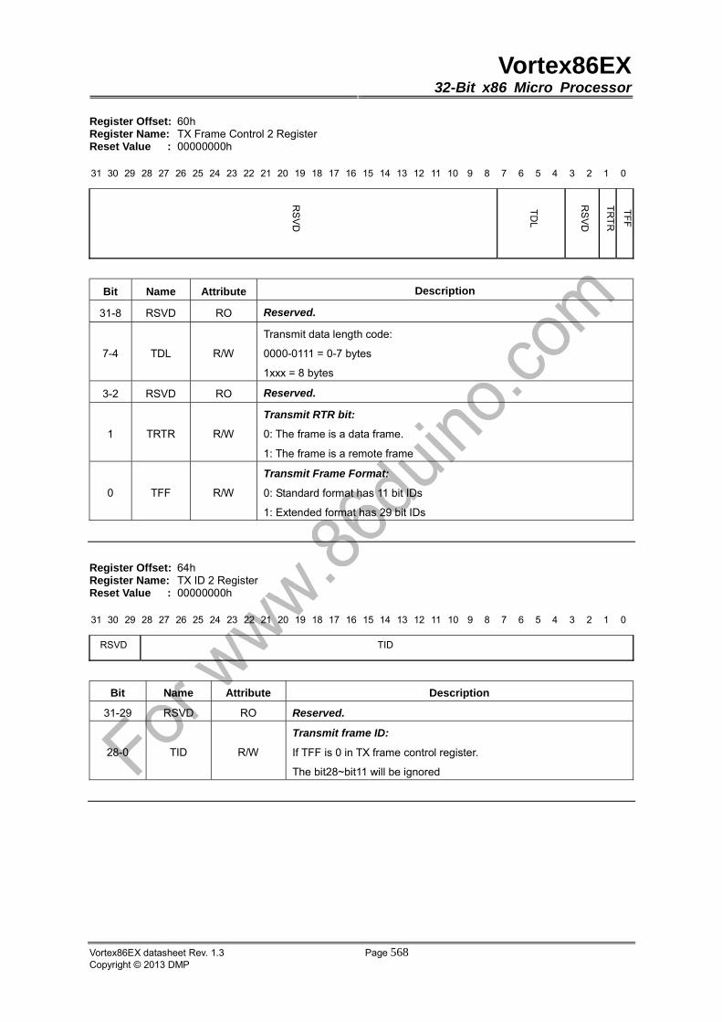
Vortex86EX32-Bit x86 Micro Processor
Vortex86EX datasheet Rev. 1.3 Page 568Copyright © 2013 DMP
Register Offset: 60h Register Name: TX Frame Control 2 Register Reset Value : 00000000h
31 30 29 28 27 26 25 24 23 22 21 20 19 18 17 16 15 14 13 12 11 10 9 8 7 6 5 4 3 2 1 0
Bit Name Attribute Description
31-8 RSVD RO Reserved.
7-4 TDL R/W
Transmit data length code:
0000-0111 = 0-7 bytes
1xxx = 8 bytes
3-2 RSVD RO Reserved.
1 TRTR R/W
Transmit RTR bit:
0: The frame is a data frame.
1: The frame is a remote frame
0 TFF R/W
Transmit Frame Format:
0: Standard format has 11 bit IDs
1: Extended format has 29 bit IDs
Register Offset: 64h Register Name: TX ID 2 Register Reset Value : 00000000h
31 30 29 28 27 26 25 24 23 22 21 20 19 18 17 16 15 14 13 12 11 10 9 8 7 6 5 4 3 2 1 0
RSVD TID
Bit Name Attribute Description
31-29 RSVD RO Reserved.
28-0 TID R/W
Transmit frame ID:
If TFF is 0 in TX frame control register.
The bit28~bit11 will be ignored

Vortex86EX32-Bit x86 Micro Processor
Vortex86EX datasheet Rev. 1.3 Page 569Copyright © 2013 DMP
Register Offset: 68h Register Name: TX Data (Low) 2 Register Reset Value : 00000000h
31 30 29 28 27 26 25 24 23 22 21 20 19 18 17 16 15 14 13 12 11 10 9 8 7 6 5 4 3 2 1 0
TXDL
Bit Name Attribute Description
31-0 TXDL R/W Transmit Data Low Dword:
Transmit valid data depends on TDL in TX frame control register.
Register Offset: 6Ch Register Name: TX Data (High) 2 Register Reset Value : 00000000h
31 30 29 28 27 26 25 24 23 22 21 20 19 18 17 16 15 14 13 12 11 10 9 8 7 6 5 4 3 2 1 0
TXDH
Bit Name Attribute Description
31-0 TXDH R/W Transmit Data High Dword:
Transmit valid data depends on TDL in TX frame control register.
Register Offset: 70h Register Name: RX Frame Type Register Reset Value : 00000000h
31 30 29 28 27 26 25 24 23 22 21 20 19 18 17 16 15 14 13 12 11 10 9 8 7 6 5 4 3 2 1 0
Bit Name Attribute Description
31-8 RSVD RO Reserved.
7-4 RDL RO
Receive data length code:
0000-0111 = 0-7 bytes
1xxx = 8 bytes
3-2 RSVD RO Reserved.
1 RRTR RO
Receive RTR bit:
0: The frame is a data frame.
1: The frame is a remote frame
0 RFF RO Receive frame format:

Vortex86EX32-Bit x86 Micro Processor
Vortex86EX datasheet Rev. 1.3 Page 570Copyright © 2013 DMP
0: Standard format has 11 bit IDs
1: Extended format has 29 bit IDs
Register Offset: 74h Register Name: RX ID Register Reset Value : 00000000h
31 30 29 28 27 26 25 24 23 22 21 20 19 18 17 16 15 14 13 12 11 10 9 8 7 6 5 4 3 2 1 0
RSVD RID
Bit Name Attribute Description
31-29 RSVD RO Reserved.
28-0 RID RO
Receive frame ID:
If RFF is 0 in RX frame type register.
The bit28~bit11 will be ignored
Register Offset: 78h Register Name: RX Data (Low) Register Reset Value : 00000000h
31 30 29 28 27 26 25 24 23 22 21 20 19 18 17 16 15 14 13 12 11 10 9 8 7 6 5 4 3 2 1 0
RXDL
Bit Name R/W Description
31-0 RXDL RO Receive Data Low Dword:
Receive valid data depends on RDL in RX frame type register.
Register Offset: 7Ch Register Name: RX Data (High) Register Reset Value : 00000000h
31 30 29 28 27 26 25 24 23 22 21 20 19 18 17 16 15 14 13 12 11 10 9 8 7 6 5 4 3 2 1 0
RXDH
Bit Name R/W Description
31-0 RXDH RO Receive data High Dword:
Receive valid data depends on RDL in RX frame type register.
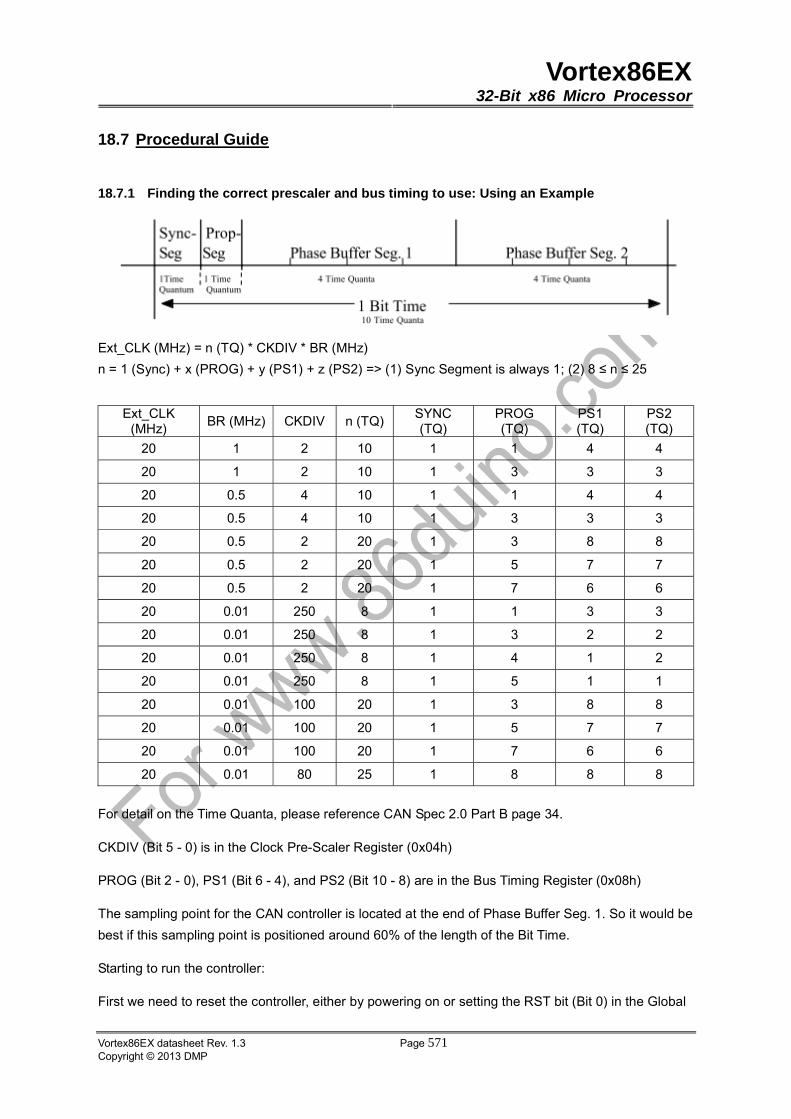
Vortex86EX32-Bit x86 Micro Processor
Vortex86EX datasheet Rev. 1.3 Page 571Copyright © 2013 DMP
18.7 Procedural Guide
18.7.1 Finding the correct prescaler and bus timing to use: Using an Example
Ext_CLK (MHz) = n (TQ) * CKDIV * BR (MHz)
n = 1 (Sync) + x (PROG) + y (PS1) + z (PS2) => (1) Sync Segment is always 1; (2) 8 ≤ n ≤ 25
Ext_CLK (MHz)
BR (MHz) CKDIV n (TQ)SYNC (TQ)
PROG (TQ)
PS1 (TQ)
PS2 (TQ)
20 1 2 10 1 1 4 4
20 1 2 10 1 3 3 3
20 0.5 4 10 1 1 4 4
20 0.5 4 10 1 3 3 3
20 0.5 2 20 1 3 8 8
20 0.5 2 20 1 5 7 7
20 0.5 2 20 1 7 6 6
20 0.01 250 8 1 1 3 3
20 0.01 250 8 1 3 2 2
20 0.01 250 8 1 4 1 2
20 0.01 250 8 1 5 1 1
20 0.01 100 20 1 3 8 8
20 0.01 100 20 1 5 7 7
20 0.01 100 20 1 7 6 6
20 0.01 80 25 1 8 8 8
For detail on the Time Quanta, please reference CAN Spec 2.0 Part B page 34.
CKDIV (Bit 5 - 0) is in the Clock Pre-Scaler Register (0x04h)
PROG (Bit 2 - 0), PS1 (Bit 6 - 4), and PS2 (Bit 10 - 8) are in the Bus Timing Register (0x08h)
The sampling point for the CAN controller is located at the end of Phase Buffer Seg. 1. So it would be
best if this sampling point is positioned around 60% of the length of the Bit Time.
Starting to run the controller:
First we need to reset the controller, either by powering on or setting the RST bit (Bit 0) in the Global
Vortex86EX32-Bit x86 Micro Processor
Vortex86EX datasheet Rev. 1.3 Page 572Copyright © 2013 DMP
Control Register (0x00h) to one. The controller is already reseted when powered up. If reseting by
RST bit, the controller has finished reseting when reading a zero from this RST bit. Importantly, the
RST bit will not reset the Identifier Filter that are set. These Identifier Filter settings has to be reset
seperately by setting the IRST bit (Bit 16) in the Global Control Register (0x00h).
After reseting and before activating the controller, we will have to set the Clock Pre-Scaler (0x04h)
and Bus Timing (0x08h) Registers. It is also recommended to set the Interrupt Enable (0x0Ch)
Register at this time too. Although there is really no harm setting the interrupt enables when the
controller is active, but still it would be better to set prior to activating.
Prior to activation, you might want to decide to set an error warning limit (Bit 7 : 0) in the Error
Warning Limit Register (0x2Ch). This will inform you when the error count has reached this limit.
However this might not mean that the controller has entered Passive State if the value was set to be
less than d’128. It is just a limit you set to inform yourself. Default is h’60.
Also prior to activation, you would need to consider if this controller acts as an detector that only
listens to the bus or as a transceiver that will send and receive datas. If it only works as a detector to
simply check if the bus transactions are correct or not, please set the RGF bit (Bit 17) in the Global
Control Register (0x00h) to zero. Then set CBA bit (Bit 1) in the Global Control Register (0x00h) to
one, by doing so the controller has started to work. If not working as a detector, please set RGF bit
(Bit 17) in the Global Control Register (0x00h) to one.
After setting the RGF bit to one, simply setting RBF bit (Bit 18) in the Global Control Register (0x00h)
to one. This will let the controller store all the messages, which are not transmiited by this controller.
If you want the controller to also store the messages that the controller sent, you could set SR bit (Bit
5) in the Global Control Register (0x00h) to one, or else leave it as zero.
If you want the optional of selective identification message storing, then please set the RBF bit (Bit 18)
in the Global Control Register (0x00h) to zero. In this controller, there is a max of 32 identifier filter
register blocks that can be used. But by using masking, it would be able to able to filter a lot more
identifiers. Set the Identifier Filter Register (0x38h) and Identifier Mask Register (0x3Ch) according to
the register bits. Then set the IFI bits (Bits 4 - 0) in the Identifier Index Register (0x34h) to point this
Identifier and its masking to one of the 32 register blocks. Also by setting the IFU bit (Bit 8) in the
Identifier Index Register (0x34h) to one will store these info to the pointed register block. When filter
is used, it should better start from register block 0.
Filter and mask truth table

Vortex86EX32-Bit x86 Micro Processor
Vortex86EX datasheet Rev. 1.3 Page 573Copyright © 2013 DMP
Mask bit n Filter bit n Message Identifier bit n Accept or Reject
0 Accept 0 0
1 Reject
0 Reject 0 1
1 Accept
0 Accept 1 0
1 Accept
0 Accept 1 1
1 Accept
Also prior to activation, you would need to consider if the transmit buffer will transmit the message
according to the identifier field priority by setting TBP bit (Bit 6) to one in the Global Control Register
(0x00h). If want to transmit message in the order of Transmit Buffer 0,1, and 2 (Transmit Buffer 0 has
the highest priority), then set TBP bit to zero, which is the default.
Also prior to activation, you would need to consider when occurring arbitration lost and error will you
want the controller to automatically retry the arbitration lost/error message again or not. When
coming accross an arbitration lost, if you want the controller to automatically retry, please set ARE bit
(Bit 7) in the Global Control Register (0x00h) to one, or else set it as zero. When encountering an
error, if you want the controller to automatically retry, please set ERE bit (Bit 8) in the Global Control
Register (0x00h) to one, or else set it as zero.
Also prior to activation, you would need to consider if you want the controller to enter power saving
mode when there is no activity on the bus. If you want this function to work, please set PSE bit (Bit 24)
in the Global Control Register (0x00h) to one, or else set to zero.
After finishing the above settings, you could set the CBA bit (Bit 1) in the Global Control Register
(0x00h) to one. This will activate the controller into working mode. If you want to redo any of the
above setting, please set the CBA bit back to zero. However setting this bit back to zero doesn’t
mean it would disactivate immidiately, for that the controller might be transmitting or receiving during
the time of the setting to zero. It would need some time to go into disactivate. Please wait until you
read back a zero in the CBA bit to confirm for the disactivation. Then simply set to one after finishing
new configurations.
18.7.2 Transmitting a message:
If there is no message being sent during the time, store the message to TX Frame Control 0 (0x40h),
TX ID 0 (0x44h), and TX Data 0 (0x48h & 0x4Ch). If there is any message that is set for transmittion
but has not yet finished transmitting, then store it into TX Frame Control 1 (0x50h), TX ID 1 (0x54h),
Vortex86EX32-Bit x86 Micro Processor
Vortex86EX datasheet Rev. 1.3 Page 574Copyright © 2013 DMP
and TX Data 1 (0x58h & 0x5Ch). If this is also filled then store to TX Frame Control 2 (0x60h), TX ID
2 (0x64h), and TX Data 2 (0x68h & 0x6Ch).
After storing the message, remember to request the transmittion by setting TBR0 (Bit 0), TBR1 (Bit 2),
or TBR2 (Bit 4) in the Request Register (0x18h) to one according to the former positioning.
If you want to abort any of the requested transmittion, you could set the TBA0 (Bit 1), TBA1 (Bit 3), or
TBA2 (Bit 5) in the Request Register (0x18h) to one according to the one you want to abort. However,
if the corresponding message has started transmitting, it will still finish transmitting and will not be
aborted.
If the TX0I bit (Bit 1), TX1I bit (Bit 2), or TX2I bit (Bit 3) in the Interrupt Status Register (0x10h) is set
to one, remember to check the corresponding Transmit Status 0 (0x1Ch), Transmit Status 1 (0x20h),
or Transmit Status 2 (0x24h) for the information on the condition of the message that has been
requested.
If completed without any error, TRC bit (Bit 0) and TC bit (Bit 2) will be set to one and the others are
zero.
If completed with error and ERE bit (Bit 8) in the Global Control Register (0x00h) is set to zero, TRC
bit (Bit 0) and BEO bit (Bit 5) will be one and the others are zero. If the ERE bit is set to one, then the
message will retry until it completes without any error or an abort comes.
If arbitration lost and ARE bit (Bit 7) in the Global Control Register (0x00h) is set to zero, TRC bit (Bit
0) and ALO bit (Bit 4) will be one and the others are zero. If the ARE bit is set to one, then the
message will retry and depending on how it finishes it would be completed with error or without error.
18.7.3 Receiving a message:
If the Receive Interrupt bit (Bit 0) in the Interrupt Status Register (0x10h) is one and the RBS bit (Bit 0)
in the Receive Status Register (0x28h) is set to one, meaning that there is any pending message
waiting to be read.
After reading the message from RX Frame Type (0x70h), RX ID (0x74h), and RX Data (0x78h &
0x7Ch), remember to set RRB bit (Bit 8) in the Request Register (0x18h) to one. This will release the
currently pending message and would update newly stored or not yet read message in the controller.
If not released, the controller will keep on sending out an interrupt saying that there is an unread
message, but in fact the message has already been read.
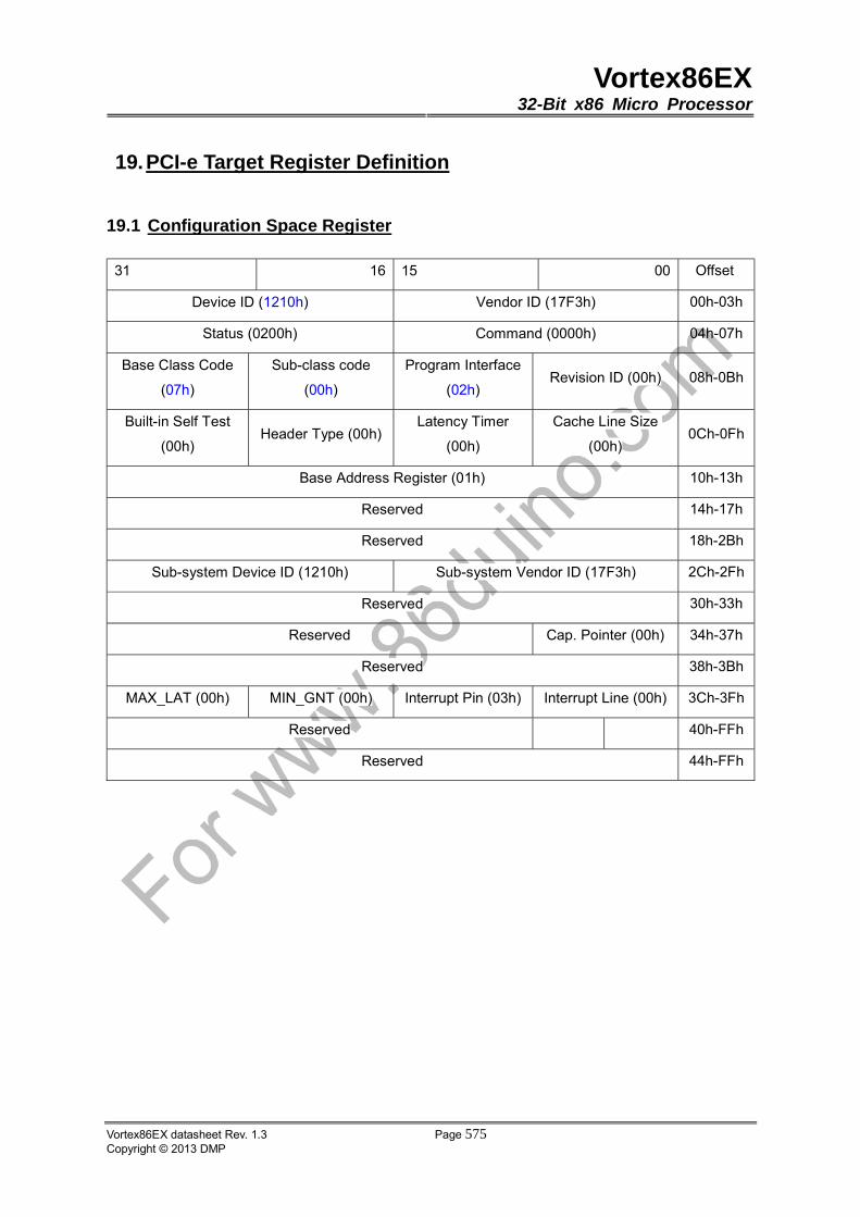
Vortex86EX32-Bit x86 Micro Processor
Vortex86EX datasheet Rev. 1.3 Page 575Copyright © 2013 DMP
19. PCI-e Target Register Definition
19.1 Configuration Space Register
31 16 15 00 Offset
Device ID (1210h) Vendor ID (17F3h) 00h-03h
Status (0200h) Command (0000h) 04h-07h
Base Class Code
(07h)
Sub-class code
(00h)
Program Interface
(02h) Revision ID (00h) 08h-0Bh
Built-in Self Test
(00h) Header Type (00h)
Latency Timer
(00h)
Cache Line Size
(00h) 0Ch-0Fh
Base Address Register (01h) 10h-13h
Reserved 14h-17h
Reserved 18h-2Bh
Sub-system Device ID (1210h) Sub-system Vendor ID (17F3h) 2Ch-2Fh
Reserved 30h-33h
Reserved Cap. Pointer (00h) 34h-37h
Reserved 38h-3Bh
MAX_LAT (00h) MIN_GNT (00h) Interrupt Pin (03h) Interrupt Line (00h) 3Ch-3Fh
Reserved 40h-FFh
Reserved 44h-FFh
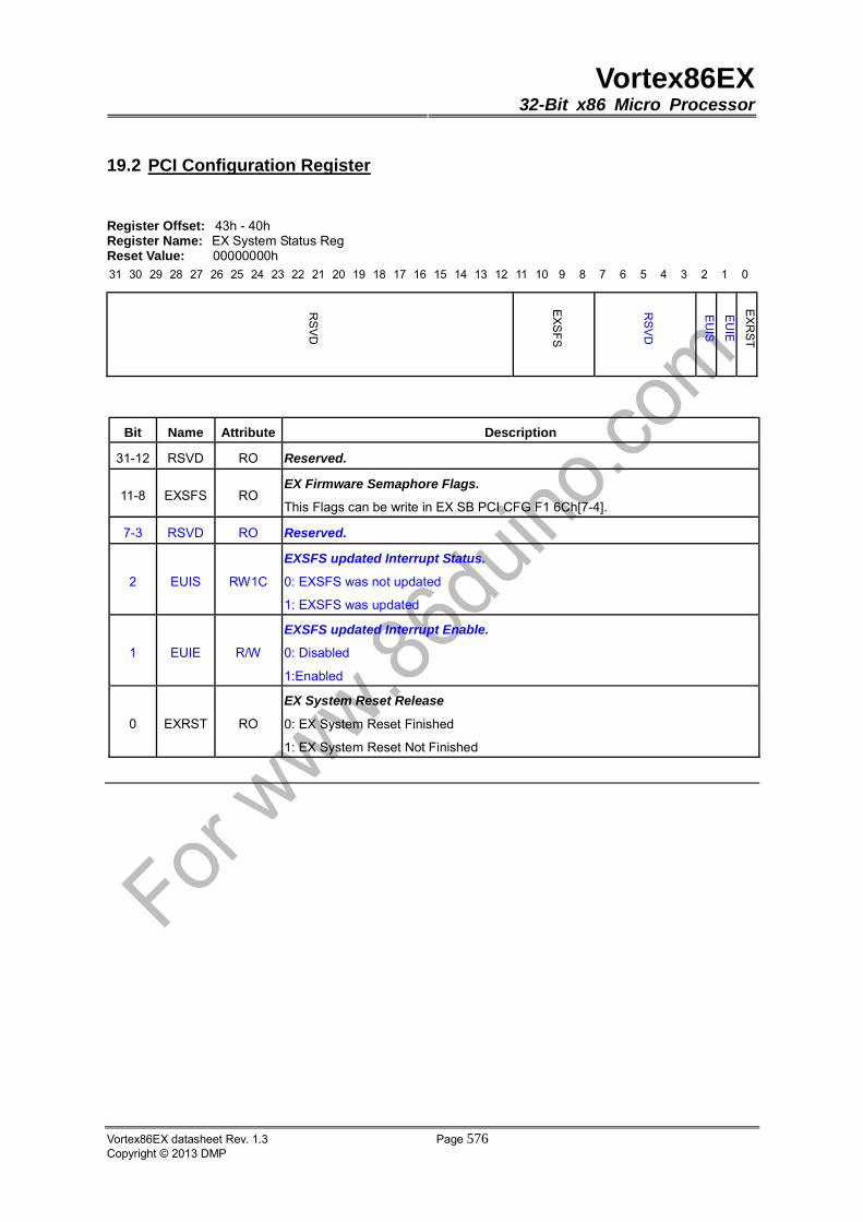
Vortex86EX32-Bit x86 Micro Processor
Vortex86EX datasheet Rev. 1.3 Page 576Copyright © 2013 DMP
19.2 PCI Configuration Register
Register Offset: 43h - 40h Register Name: EX System Status Reg Reset Value: 00000000h 31 30 29 28 27 26 25 24 23 22 21 20 19 18 17 16 15 14 13 12 11 10 9 8 7 6 5 4 3 2 1 0
Bit Name Attribute Description
31-12 RSVD RO Reserved.
11-8 EXSFS RO EX Firmware Semaphore Flags.
This Flags can be write in EX SB PCI CFG F1 6Ch[7-4].
7-3 RSVD RO Reserved.
2 EUIS RW1C
EXSFS updated Interrupt Status.
0: EXSFS was not updated
1: EXSFS was updated
1 EUIE R/W
EXSFS updated Interrupt Enable.
0: Disabled
1:Enabled
0 EXRST RO
EX System Reset Release
0: EX System Reset Finished
1: EX System Reset Not Finished
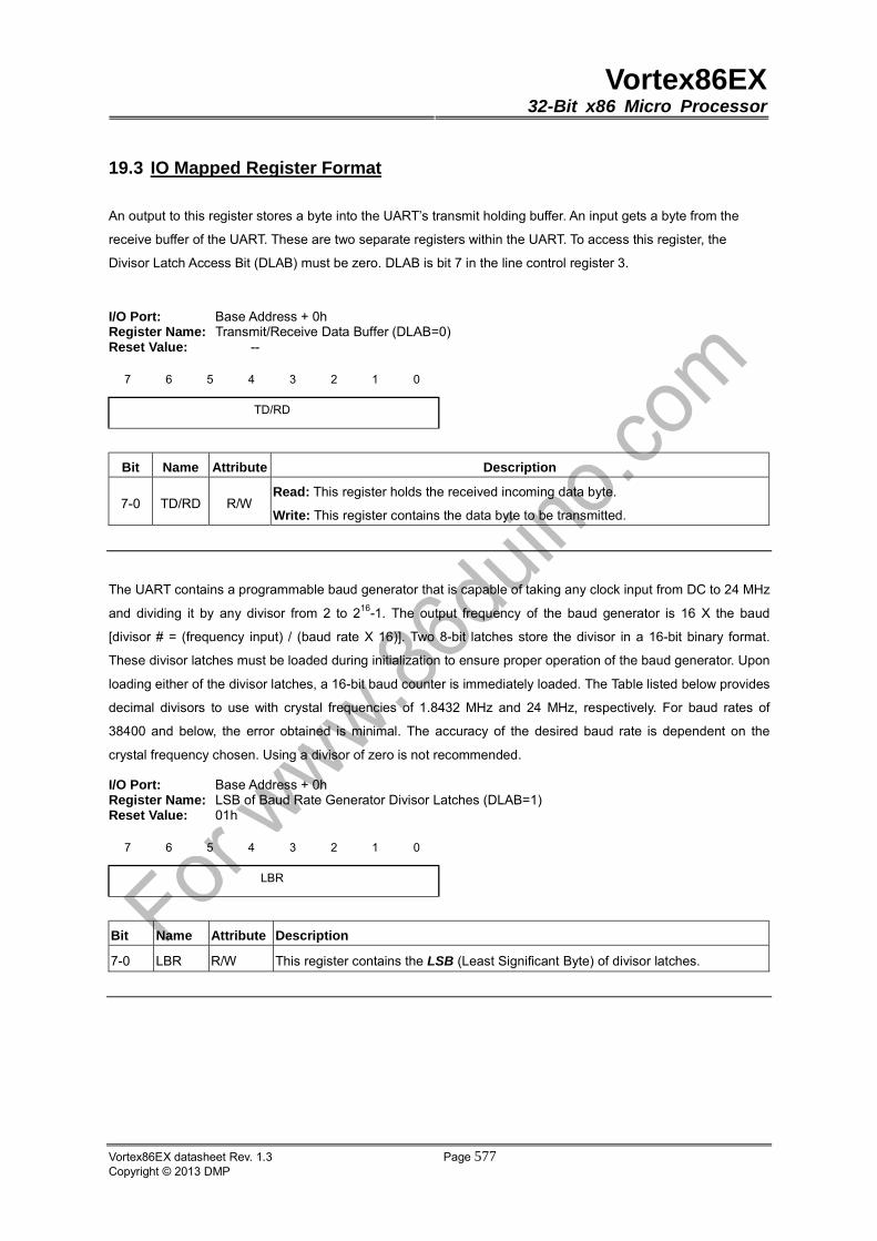
Vortex86EX32-Bit x86 Micro Processor
Vortex86EX datasheet Rev. 1.3 Page 577Copyright © 2013 DMP
19.3 IO Mapped Register Format
An output to this register stores a byte into the UART’s transmit holding buffer. An input gets a byte from the
receive buffer of the UART. These are two separate registers within the UART. To access this register, the
Divisor Latch Access Bit (DLAB) must be zero. DLAB is bit 7 in the line control register 3.
I/O Port: Base Address + 0h Register Name: Transmit/Receive Data Buffer (DLAB=0) Reset Value: --
7 6 5 4 3 2 1 0
TD/RD
Bit Name Attribute Description
7-0 TD/RD R/W Read: This register holds the received incoming data byte.
Write: This register contains the data byte to be transmitted.
The UART contains a programmable baud generator that is capable of taking any clock input from DC to 24 MHz
and dividing it by any divisor from 2 to 216-1. The output frequency of the baud generator is 16 X the baud
[divisor # = (frequency input) / (baud rate X 16)]. Two 8-bit latches store the divisor in a 16-bit binary format.
These divisor latches must be loaded during initialization to ensure proper operation of the baud generator. Upon
loading either of the divisor latches, a 16-bit baud counter is immediately loaded. The Table listed below provides
decimal divisors to use with crystal frequencies of 1.8432 MHz and 24 MHz, respectively. For baud rates of
38400 and below, the error obtained is minimal. The accuracy of the desired baud rate is dependent on the
crystal frequency chosen. Using a divisor of zero is not recommended.
I/O Port: Base Address + 0h Register Name: LSB of Baud Rate Generator Divisor Latches (DLAB=1) Reset Value: 01h
7 6 5 4 3 2 1 0
LBR
Bit Name Attribute Description
7-0 LBR R/W This register contains the LSB (Least Significant Byte) of divisor latches.
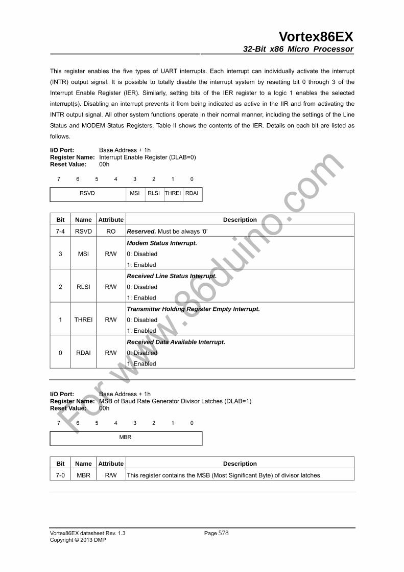
Vortex86EX32-Bit x86 Micro Processor
Vortex86EX datasheet Rev. 1.3 Page 578Copyright © 2013 DMP
This register enables the five types of UART interrupts. Each interrupt can individually activate the interrupt
(INTR) output signal. It is possible to totally disable the interrupt system by resetting bit 0 through 3 of the
Interrupt Enable Register (IER). Similarly, setting bits of the IER register to a logic 1 enables the selected
interrupt(s). Disabling an interrupt prevents it from being indicated as active in the IIR and from activating the
INTR output signal. All other system functions operate in their normal manner, including the settings of the Line
Status and MODEM Status Registers. Table II shows the contents of the IER. Details on each bit are listed as
follows.
I/O Port: Base Address + 1h Register Name: Interrupt Enable Register (DLAB=0) Reset Value: 00h
7 6 5 4 3 2 1 0
RSVD MSI RLSI THREI RDAI
Bit Name Attribute Description
7-4 RSVD RO Reserved. Must be always ‘0’
3 MSI R/W
Modem Status Interrupt.
0: Disabled
1: Enabled
2 RLSI R/W
Received Line Status Interrupt.
0: Disabled
1: Enabled
1 THREI R/W
Transmitter Holding Register Empty Interrupt.
0: Disabled
1: Enabled
0 RDAI R/W
Received Data Available Interrupt.
0: Disabled
1: Enabled
I/O Port: Base Address + 1h Register Name: MSB of Baud Rate Generator Divisor Latches (DLAB=1) Reset Value: 00h
7 6 5 4 3 2 1 0
MBR
Bit Name Attribute Description
7-0 MBR R/W This register contains the MSB (Most Significant Byte) of divisor latches.
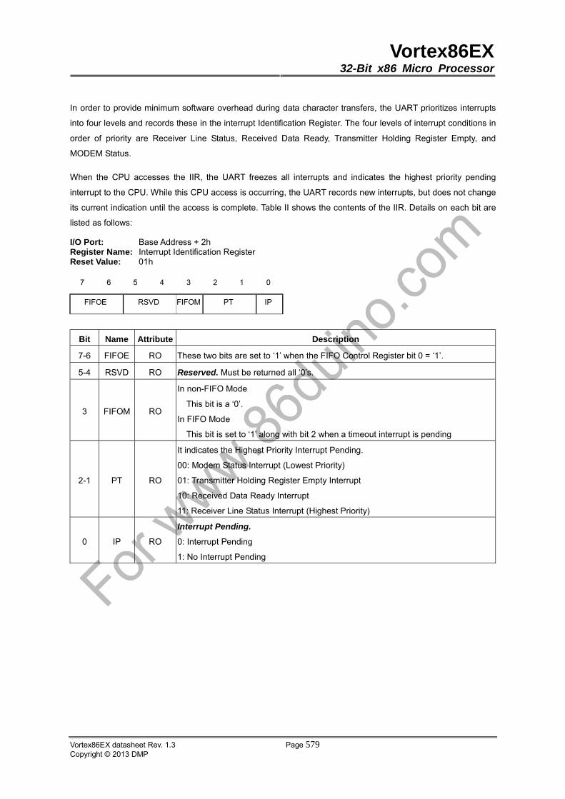
Vortex86EX32-Bit x86 Micro Processor
Vortex86EX datasheet Rev. 1.3 Page 579Copyright © 2013 DMP
In order to provide minimum software overhead during data character transfers, the UART prioritizes interrupts
into four levels and records these in the interrupt Identification Register. The four levels of interrupt conditions in
order of priority are Receiver Line Status, Received Data Ready, Transmitter Holding Register Empty, and
MODEM Status.
When the CPU accesses the IIR, the UART freezes all interrupts and indicates the highest priority pending
interrupt to the CPU. While this CPU access is occurring, the UART records new interrupts, but does not change
its current indication until the access is complete. Table II shows the contents of the IIR. Details on each bit are
listed as follows:
I/O Port: Base Address + 2h Register Name: Interrupt Identification Register Reset Value: 01h
7 6 5 4 3 2 1 0
FIFOE RSVD FIFOM PT IP
Bit Name Attribute Description
7-6 FIFOE RO These two bits are set to ‘1’ when the FIFO Control Register bit 0 = ‘1’.
5-4 RSVD RO Reserved. Must be returned all ‘0’s.
3 FIFOM RO
In non-FIFO Mode
This bit is a ‘0’.
In FIFO Mode
This bit is set to ‘1’ along with bit 2 when a timeout interrupt is pending
2-1 PT RO
It indicates the Highest Priority Interrupt Pending.
00: Modem Status Interrupt (Lowest Priority)
01: Transmitter Holding Register Empty Interrupt
10: Received Data Ready Interrupt
11: Receiver Line Status Interrupt (Highest Priority)
0 IP RO
Interrupt Pending.
0: Interrupt Pending
1: No Interrupt Pending
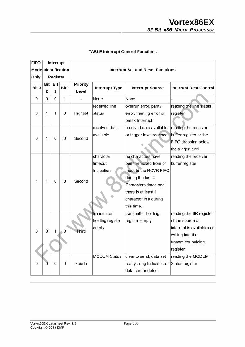
Vortex86EX32-Bit x86 Micro Processor
Vortex86EX datasheet Rev. 1.3 Page 580Copyright © 2013 DMP
TABLE Interrupt Control Functions
FIFO
Mode
Only
Interrupt
Identification
Register
Interrupt Set and Reset Functions
Bit 3Bit
2
Bit
1Bit0
Priority
Level Interrupt Type Interrupt Source Interrupt Rest Control
0 0 0 1 - None None -
0 1 1 0 Highest
received line
status
overrun error, parity
error, framing error or
break Interrupt
reading the line status
register
0 1 0 0 Second
received data
available
received data available
or trigger level reached
reading the receiver
buffer register or the
FIFO dropping below
the trigger level
1 1 0 0 Second
character
timeout
Indication
no characters have
been removed from or
Input to the RCVR FIFO
during the last 4
Characters times and
there is at least 1
character in it during
this time.
reading the receiver
buffer register
0 0 1 0 Third
transmitter
holding register
empty
transmitter holding
register empty
reading the IIR register
(if the source of
interrupt is available) or
writing into the
transmitter holding
register
0 0 0 0 Fourth
MODEM Status clear to send, data set
ready , ring Indicator, or
data carrier detect
reading the MODEM
Status register
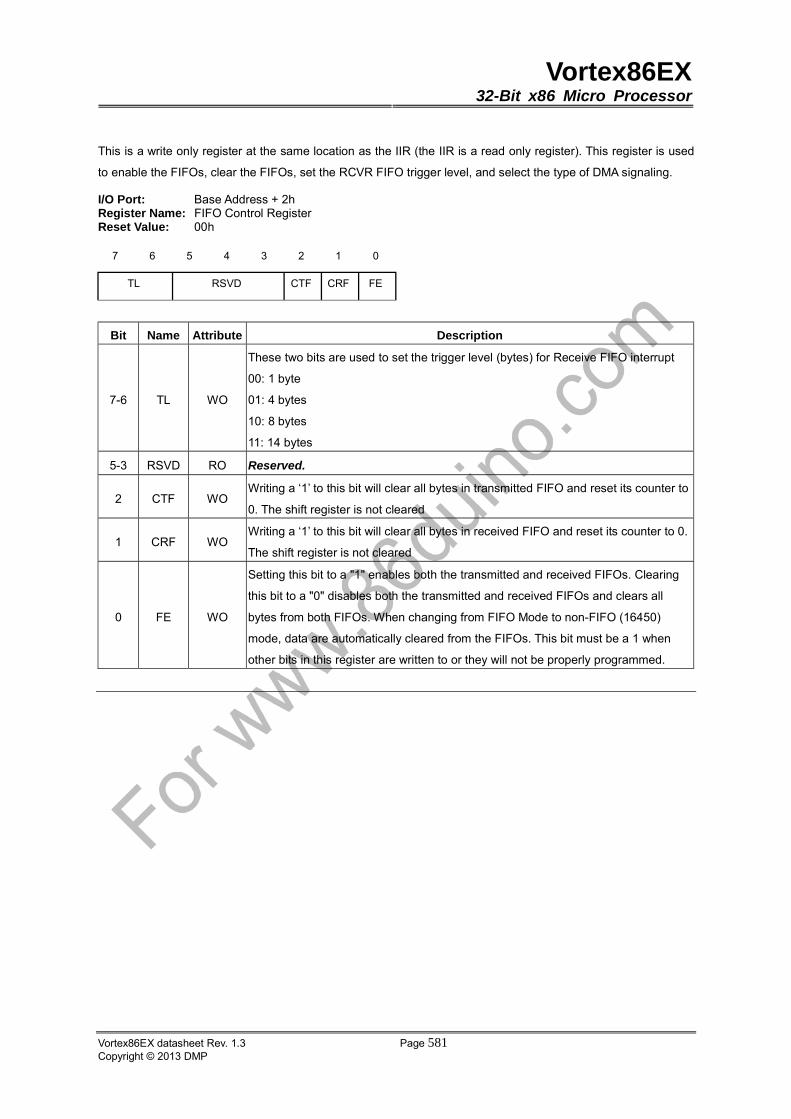
Vortex86EX32-Bit x86 Micro Processor
Vortex86EX datasheet Rev. 1.3 Page 581Copyright © 2013 DMP
This is a write only register at the same location as the IIR (the IIR is a read only register). This register is used
to enable the FIFOs, clear the FIFOs, set the RCVR FIFO trigger level, and select the type of DMA signaling.
I/O Port: Base Address + 2h Register Name: FIFO Control Register Reset Value: 00h
7 6 5 4 3 2 1 0
TL RSVD CTF CRF FE
Bit Name Attribute Description
7-6 TL WO
These two bits are used to set the trigger level (bytes) for Receive FIFO interrupt
00: 1 byte
01: 4 bytes
10: 8 bytes
11: 14 bytes
5-3 RSVD RO Reserved.
2 CTF WO Writing a ‘1’ to this bit will clear all bytes in transmitted FIFO and reset its counter to
0. The shift register is not cleared
1 CRF WO Writing a ‘1’ to this bit will clear all bytes in received FIFO and reset its counter to 0.
The shift register is not cleared
0 FE WO
Setting this bit to a "1" enables both the transmitted and received FIFOs. Clearing
this bit to a "0" disables both the transmitted and received FIFOs and clears all
bytes from both FIFOs. When changing from FIFO Mode to non-FIFO (16450)
mode, data are automatically cleared from the FIFOs. This bit must be a 1 when
other bits in this register are written to or they will not be properly programmed.
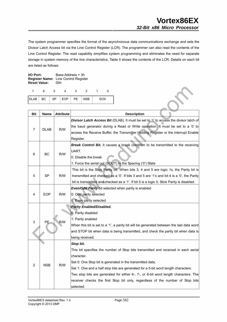
Vortex86EX32-Bit x86 Micro Processor
Vortex86EX datasheet Rev. 1.3 Page 582Copyright © 2013 DMP
The system programmer specifies the format of the asynchronous data communications exchange and sets the
Divisor Latch Access bit via the Line Control Register (LCR). The programmer can also read the contents of the
Line Control Register. The read capability simplifies system programming and eliminates the need for separate
storage in system memory of the line characteristics. Table II shows the contents of the LCR. Details on each bit
are listed as follows:
I/O Port: Base Address + 3h Register Name: Line Control Register Reset Value: 00h
7 6 5 4 3 2 1 0
DLAB BC SP EOP PE NSB SCN
Bit Name Attribute Description
7 DLAB R/W
Divisor Latch Access Bit (DLAB). It must be set to ‘1’ to access the divisor latch of
the baud generator during a Read or Write operation. It must be set to a ‘0’ to
access the Receive Buffer, the Transmitter Holding Register or the interrupt Enable
Register.
6 BC R/W
Break Control Bit. It causes a break condition to be transmitted to the receiving
UART.
0: Disable the break
1: Force the serial out (SOUT) to the Spacing (‘0’) State
5 SP R/W
This bit is the Stick Parity bit. When bits 3, 4 and 5 are logic 1s, the Parity bit is
transmitted and checked as a ‘0’. If bits 3 and 5 are ‘1’s and bit 4 is a ‘0’, the Parity
bit is transmitted and checked as a ‘1’. If bit 5 is a logic 0, Stick Parity is disabled.
4 EOP R/W
Even/Odd Parity bit selected when parity is enabled
0: Odd parity selected
1: Even parity selected
3 PE R/W
Parity Enabled/Disabled.
0: Parity disabled
1: Parity enabled
When this bit is set to a ‘1’, a parity bit will be generated between the last data word
and STOP bit when data is being transmitted, and check the parity bit when data is
being received.
2 NSB R/W
Stop bit.
This bit specifies the number of Stop bits transmitted and received in each serial
character.
Set 0: One Stop bit is generated in the transmitted data.
Set 1: One and a half stop bits are generated for a 5-bit word length characters.
Two stop bits are generated for either 6-, 7-, or 8-bit word length characters. The
receiver checks the first Stop bit only, regardless of the number of Stop bits
selected.
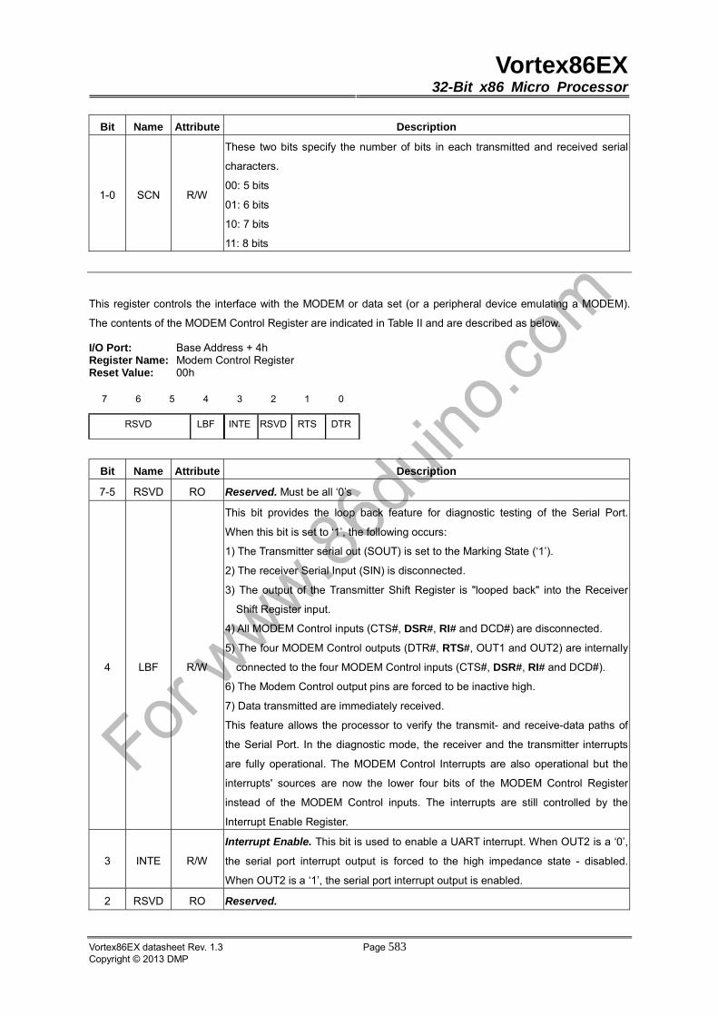
Vortex86EX32-Bit x86 Micro Processor
Vortex86EX datasheet Rev. 1.3 Page 583Copyright © 2013 DMP
Bit Name Attribute Description
1-0 SCN R/W
These two bits specify the number of bits in each transmitted and received serial
characters.
00: 5 bits
01: 6 bits
10: 7 bits
11: 8 bits
This register controls the interface with the MODEM or data set (or a peripheral device emulating a MODEM).
The contents of the MODEM Control Register are indicated in Table II and are described as below.
I/O Port: Base Address + 4h Register Name: Modem Control Register Reset Value: 00h
7 6 5 4 3 2 1 0
RSVD LBF INTE RSVD RTS DTR
Bit Name Attribute Description
7-5 RSVD RO Reserved. Must be all ‘0’s
4 LBF R/W
This bit provides the loop back feature for diagnostic testing of the Serial Port.
When this bit is set to ‘1’, the following occurs:
1) The Transmitter serial out (SOUT) is set to the Marking State (‘1’).
2) The receiver Serial Input (SIN) is disconnected.
3) The output of the Transmitter Shift Register is "looped back" into the Receiver
Shift Register input.
4) All MODEM Control inputs (CTS#, DSR#, RI# and DCD#) are disconnected.
5) The four MODEM Control outputs (DTR#, RTS#, OUT1 and OUT2) are internally
connected to the four MODEM Control inputs (CTS#, DSR#, RI# and DCD#).
6) The Modem Control output pins are forced to be inactive high.
7) Data transmitted are immediately received.
This feature allows the processor to verify the transmit- and receive-data paths of
the Serial Port. In the diagnostic mode, the receiver and the transmitter interrupts
are fully operational. The MODEM Control Interrupts are also operational but the
interrupts' sources are now the lower four bits of the MODEM Control Register
instead of the MODEM Control inputs. The interrupts are still controlled by the
Interrupt Enable Register.
3 INTE R/W
Interrupt Enable. This bit is used to enable a UART interrupt. When OUT2 is a ‘0’,
the serial port interrupt output is forced to the high impedance state - disabled.
When OUT2 is a ‘1’, the serial port interrupt output is enabled.
2 RSVD RO Reserved.
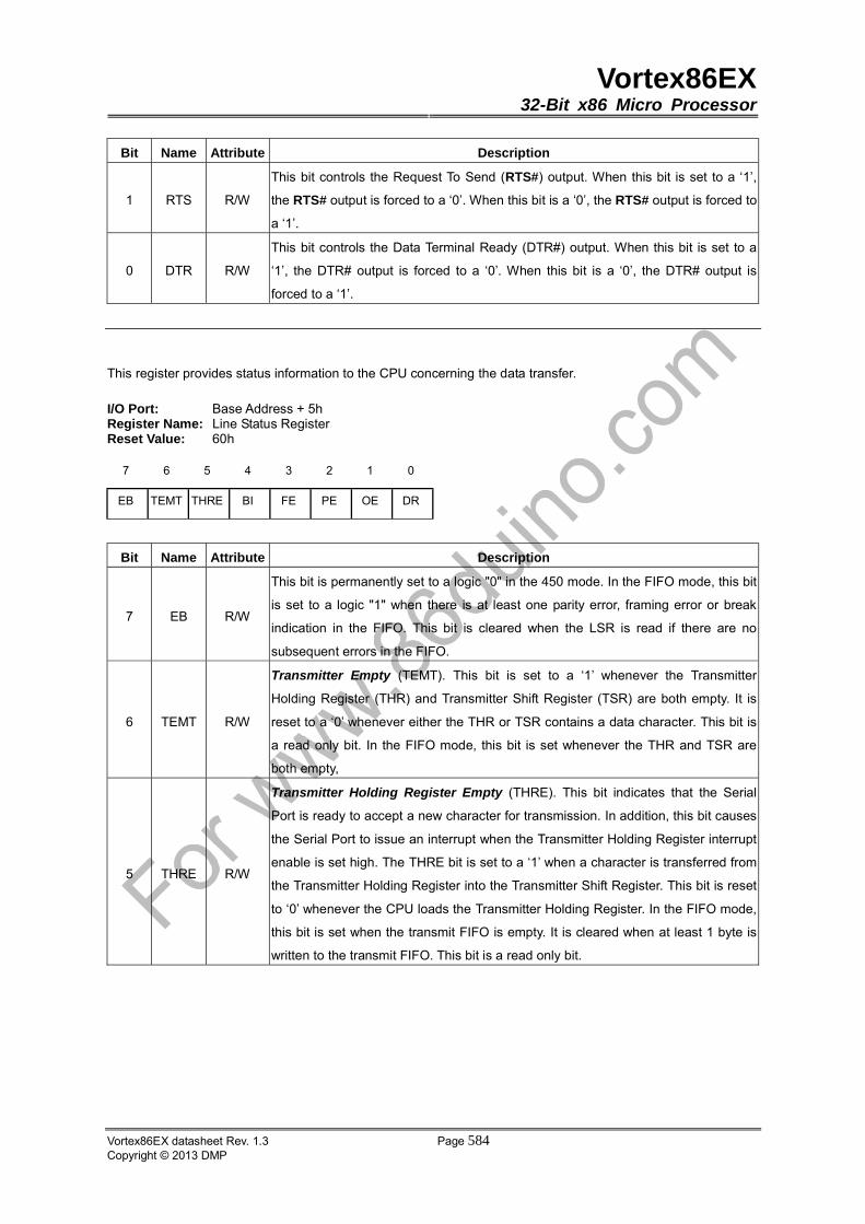
Vortex86EX32-Bit x86 Micro Processor
Vortex86EX datasheet Rev. 1.3 Page 584Copyright © 2013 DMP
Bit Name Attribute Description
1 RTS R/W
This bit controls the Request To Send (RTS#) output. When this bit is set to a ‘1’,
the RTS# output is forced to a ‘0’. When this bit is a ‘0’, the RTS# output is forced to
a ‘1’.
0 DTR R/W
This bit controls the Data Terminal Ready (DTR#) output. When this bit is set to a
‘1’, the DTR# output is forced to a ‘0’. When this bit is a ‘0’, the DTR# output is
forced to a ‘1’.
This register provides status information to the CPU concerning the data transfer.
I/O Port: Base Address + 5h Register Name: Line Status Register Reset Value: 60h
7 6 5 4 3 2 1 0
EB TEMT THRE BI FE PE OE DR
Bit Name Attribute Description
7 EB R/W
This bit is permanently set to a logic "0" in the 450 mode. In the FIFO mode, this bit
is set to a logic "1" when there is at least one parity error, framing error or break
indication in the FIFO. This bit is cleared when the LSR is read if there are no
subsequent errors in the FIFO.
6 TEMT R/W
Transmitter Empty (TEMT). This bit is set to a ‘1’ whenever the Transmitter
Holding Register (THR) and Transmitter Shift Register (TSR) are both empty. It is
reset to a ‘0’ whenever either the THR or TSR contains a data character. This bit is
a read only bit. In the FIFO mode, this bit is set whenever the THR and TSR are
both empty,
5 THRE R/W
Transmitter Holding Register Empty (THRE). This bit indicates that the Serial
Port is ready to accept a new character for transmission. In addition, this bit causes
the Serial Port to issue an interrupt when the Transmitter Holding Register interrupt
enable is set high. The THRE bit is set to a ‘1’ when a character is transferred from
the Transmitter Holding Register into the Transmitter Shift Register. This bit is reset
to ‘0’ whenever the CPU loads the Transmitter Holding Register. In the FIFO mode,
this bit is set when the transmit FIFO is empty. It is cleared when at least 1 byte is
written to the transmit FIFO. This bit is a read only bit.
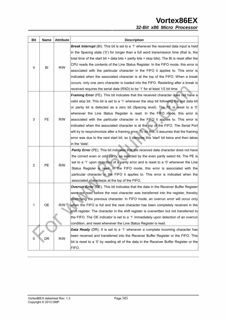
Vortex86EX32-Bit x86 Micro Processor
Vortex86EX datasheet Rev. 1.3 Page 585Copyright © 2013 DMP
Bit Name Attribute Description
4 BI R/W
Break Interrupt (BI). This bit is set to a ‘1’ whenever the received data input is held
in the Spacing state (‘0’) for longer than a full word transmission time (that is, the
total time of the start bit + data bits + parity bits + stop bits). The BI is reset after the
CPU reads the contents of the Line Status Register. In the FIFO mode, this error is
associated with the particular character in the FIFO it applies to. This error is
indicated when the associated character is at the top of the FIFO. When a break
occurs, only one zero character is loaded into the FIFO. Restarting after a break is
received requires the serial data (RXD) to be ‘1’ for at least 1/2 bit time.
3 FE R/W
Framing Error (FE). This bit indicates that the received character does not have a
valid stop bit. This bit is set to a ‘1’ whenever the stop bit following the last data bit
or parity bit is detected as a zero bit (Spacing level). The FE is reset to a ‘0’
whenever the Line Status Register is read. In the FIFO mode, this error is
associated with the particular character in the FIFO it applies to. This error is
indicated when the associated character is at the top of the FIFO. The Serial Port
will try to resynchronize after a framing error. To do this, it assumes that the framing
error was due to the next start bit, so it samples this 'start' bit twice and then takes
in the 'data'.
2 PE R/W
Parity Error (PE). This bit indicates that the received data character does not have
the correct even or odd parity, as selected by the even parity select bit. The PE is
set to a ‘1’ upon detection of a parity error and is reset to a ‘0’ whenever the Line
Status Register is read. In the FIFO mode, this error is associated with the
particular character in the FIFO it applies to. This error is indicated when the
associated character is at the top of the FIFO.
1 OE R/W
Overrun Error (OE). This bit indicates that the data in the Receiver Buffer Register
were not read before the next character was transferred into the register, thereby
destroying the previous character. In FIFO mode, an overrun error will occur only
when the FIFO is full and the next character has been completely received in the
shift register. The character in the shift register is overwritten but not transferred to
the FIFO. The OE indicator is set to a ‘1’ immediately upon detection of an overrun
condition, and reset whenever the Line Status Register is read.
0 DR R/W
Data Ready (DR). It is set to a ‘1’ whenever a complete incoming character has
been received and transferred into the Receiver Buffer Register or the FIFO. This
bit is reset to a ‘0’ by reading all of the data in the Receiver Buffer Register or the
FIFO.
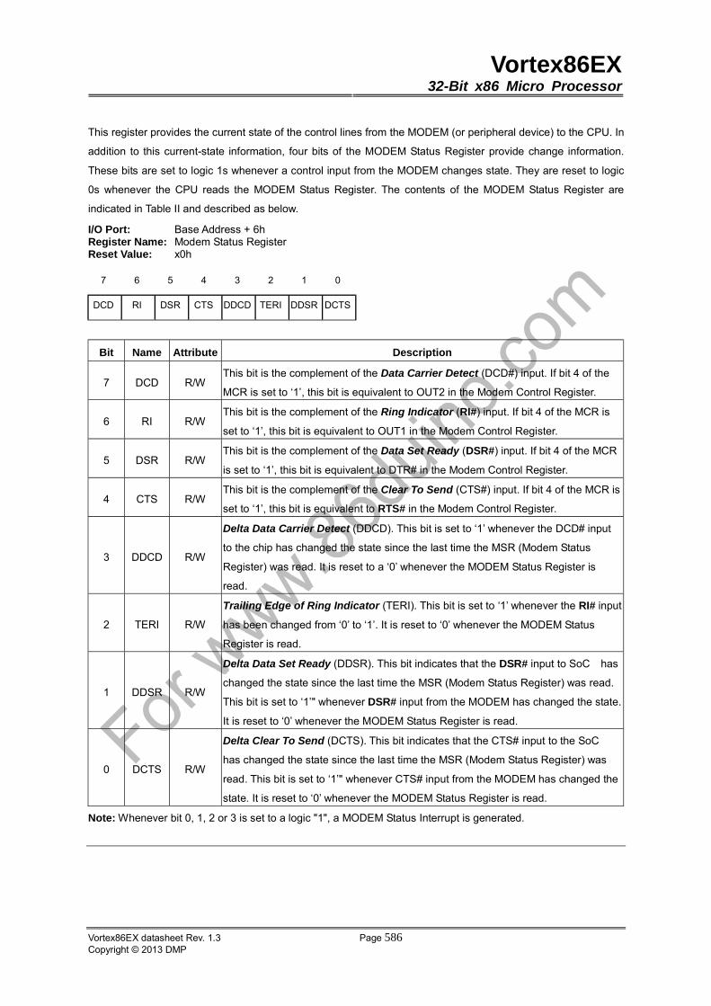
Vortex86EX32-Bit x86 Micro Processor
Vortex86EX datasheet Rev. 1.3 Page 586Copyright © 2013 DMP
This register provides the current state of the control lines from the MODEM (or peripheral device) to the CPU. In
addition to this current-state information, four bits of the MODEM Status Register provide change information.
These bits are set to logic 1s whenever a control input from the MODEM changes state. They are reset to logic
0s whenever the CPU reads the MODEM Status Register. The contents of the MODEM Status Register are
indicated in Table II and described as below.
I/O Port: Base Address + 6h Register Name: Modem Status Register Reset Value: x0h
7 6 5 4 3 2 1 0
DCD RI DSR CTS DDCD TERI DDSR DCTS
Bit Name Attribute Description
7 DCD R/W This bit is the complement of the Data Carrier Detect (DCD#) input. If bit 4 of the
MCR is set to ‘1’, this bit is equivalent to OUT2 in the Modem Control Register.
6 RI R/W This bit is the complement of the Ring Indicator (RI#) input. If bit 4 of the MCR is
set to ‘1’, this bit is equivalent to OUT1 in the Modem Control Register.
5 DSR R/W This bit is the complement of the Data Set Ready (DSR#) input. If bit 4 of the MCR
is set to ‘1’, this bit is equivalent to DTR# in the Modem Control Register.
4 CTS R/W This bit is the complement of the Clear To Send (CTS#) input. If bit 4 of the MCR is
set to ‘1’, this bit is equivalent to RTS# in the Modem Control Register.
3 DDCD R/W
Delta Data Carrier Detect (DDCD). This bit is set to ‘1’ whenever the DCD# input
to the chip has changed the state since the last time the MSR (Modem Status
Register) was read. It is reset to a ‘0’ whenever the MODEM Status Register is
read.
2 TERI R/W
Trailing Edge of Ring Indicator (TERI). This bit is set to ‘1’ whenever the RI# input
has been changed from ‘0’ to ‘1’. It is reset to ‘0’ whenever the MODEM Status
Register is read.
1 DDSR R/W
Delta Data Set Ready (DDSR). This bit indicates that the DSR# input to SoC has
changed the state since the last time the MSR (Modem Status Register) was read.
This bit is set to ‘1’" whenever DSR# input from the MODEM has changed the state.
It is reset to ‘0’ whenever the MODEM Status Register is read.
0 DCTS R/W
Delta Clear To Send (DCTS). This bit indicates that the CTS# input to the SoC
has changed the state since the last time the MSR (Modem Status Register) was
read. This bit is set to ‘1’" whenever CTS# input from the MODEM has changed the
state. It is reset to ‘0’ whenever the MODEM Status Register is read.
Note: Whenever bit 0, 1, 2 or 3 is set to a logic "1", a MODEM Status Interrupt is generated.

Vortex86EX32-Bit x86 Micro Processor
Vortex86EX datasheet Rev. 1.3 Page 587Copyright © 2013 DMP
This 8-bit Read/Write Register does not control the UART in any way. It is intended as a scratchpad register
used by the programmer to hold data temporarily.
I/O Port: Base Address + 7h Register Name: Scratchpad Register Reset Value: --
7 6 5 4 3 2 1 0
SR
Bit Name Attribute Description
7-0 SR R/W
This 8-bit read/write register has no effect on the operation of the Serial Port. It is
intended as a scratchpad register to be used by the programmer to hold data
temporarily.
Vortex86EX32-Bit x86 Micro Processor
Vortex86EX datasheet Rev. 1.3 Page 588Copyright © 2013 DMP
20. MISC Control Unit
20.1 Overview
A MISC control unit provides Motion Controller and Full-Duplex SPI .
20.2 Features
Support 4 Motion Controllers (Bus 0, Device 16, Function 0)
Support one Full-Duplex SPI (Bus 0, Device 16, Function 1)
20.3 MISC PCI Configuration Registers Definition
20.3.1 Motion Controller Configuration Space Register
31 16 15 00 Offset
Device ID (1331h) Vendor ID (17F3h) 00h-03h
Status (0200h) Command (0000h) 04h-07h
Base Class Code
(FFh) Sub-class code (FFh)
Program Interface
(00h) Revision ID (00h) 08h-0Bh
Built-in Self Test
(00h) Header Type (80h) Latency Timer (00h)
Cache Line Size
(00h) 0Ch-0Fh
I/O Base Address Register (01h) 10h-13h
Memory Base Address Register (00h) 14h-17h
Reserved 18h-2Bh
Sub-system Device ID (1330h) Sub-system Vendor ID (17F3h) 2Ch-2Fh
Reserved 30h-33h
Reserved Cap. Pointer (00h) 34h-37h
Reserved 38h-3Bh
MAX_LAT (00h) MIN_GNT (00h) Interrupt Pin (01h) Interrupt Line (00h) 3Ch-3Fh
Register R/W Control
(00h)
Test Mode Enable
(00h) MC Power Down (0000h) 40h-43h
Reserved MC Port State Control (000000h) 44h-47h
Reserved 48h-FFh
Vortex86EX32-Bit x86 Micro Processor
Vortex86EX datasheet Rev. 1.3 Page 589Copyright © 2013 DMP
20.3.2 Full-Duplex SPI Configuration Space Register
31 16 15 00 Offset
Device ID (1710h) Vendor ID (17F3h) 00h-03h
Status (0200h) Command (0000h) 04h-07h
Base Class Code
(FFh)
Sub-class code
(FFh)
Program Interface
(00h) Revision ID (01h) 08h-0Bh
Built-in Self Test
(00h) Header Type (00h)
Latency Timer
(00h)
Cache Line Size
(00h) 0Ch-0Fh
Base Address Register (01h) 10h-13h
Base Address Register (00h) 14h-17h
Reserved 18h-2Bh
Sub-system Device ID (1710h) Sub-system Vendor ID (17F3h) 2Ch-2Fh
Reserved 30h-33h
Reserved Cap. Pointer (00h) 34h-37h
Reserved 38h-3Bh
MAX_LAT (00h) MIN_GNT (00h) Interrupt Pin (02h) Interrupt Line (00h) 3Ch-3Fh
Register R/W
Control (00h) Reserved 40h-FFh
Vortex86EX32-Bit x86 Micro Processor
Vortex86EX datasheet Rev. 1.3 Page 590Copyright © 2013 DMP
20.4 Full-Duplex SPI Controller
20.4.1 Timing diagram for each mode
CPOL = 0
CPOL = 1
MISO
MOSI
MOSI
MISO
MOSI
MISO
MOSI
MISO
CPHA = 0
CPHA = 1
CPHA = 0
CPHA = 1
SS
SMOD =0
SMOD =1
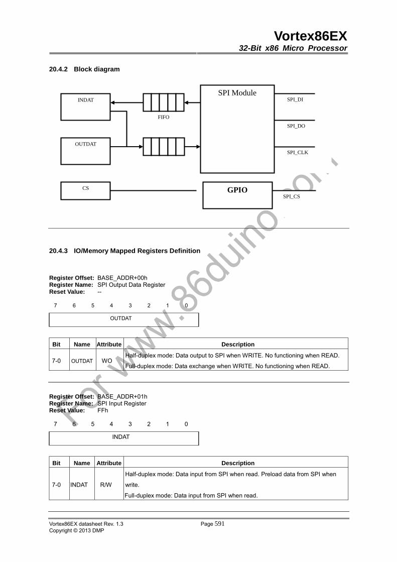
Vortex86EX32-Bit x86 Micro Processor
Vortex86EX datasheet Rev. 1.3 Page 591Copyright © 2013 DMP
20.4.2 Block diagram
20.4.3 IO/Memory Mapped Registers Definition
Register Offset: BASE_ADDR+00h Register Name: SPI Output Data Register Reset Value: --
7 6 5 4 3 2 1 0
OUTDAT
Bit Name Attribute Description
7-0 OUTDAT WO Half-duplex mode: Data output to SPI when WRITE. No functioning when READ.
Full-duplex mode: Data exchange when WRITE. No functioning when READ.
Register Offset: BASE_ADDR+01h Register Name: SPI Input Register Reset Value: FFh
7 6 5 4 3 2 1 0
INDAT
Bit Name Attribute Description
7-0 INDAT R/W
Half-duplex mode: Data input from SPI when read. Preload data from SPI when
write.
Full-duplex mode: Data input from SPI when read.
FIFO
SPI_DI
SPI_DO
SPI_CLK
SPI_CS
SPI Module INDAT
OUTDAT
CS GPIO
Vortex86EX32-Bit x86 Micro Processor
Vortex86EX datasheet Rev. 1.3 Page 592Copyright © 2013 DMP
It is not recommended to modify this register when SPI operation.
Register Offset: BASE_ADDR+02h Register Name: SPI FIFO & Clock Divide Low Byte Register Reset Value: 12h
7 6 5 4 3 2 1 0
RSVD FIEN CKDIV_L
Bit Name Attribute Description
7-4 RSVD RO Reserved.
4 FIEN R/W FIFO mode enable when set.
3-0 CKDIV_L R/W
SPI Clock Divided Low Byte.
The SPI clock is SOURCE clock/(2 * SPI clock divided) , 0 is not allowed. H/W will
auto change to 1 when CKDIV_H=0, CKDIV_M=0 and CKDIV_L=0 , therefore the
programming flow of set SPI clock will be write CKDIV_H and CKDIV_M first then
CKDIV_L.
Register Offset: BASE_ADDR+03h Register Name: SPI Status Register Reset Value: 18h
7 6 5 4 3 2 1 0
BUSY OFIFU IDR TDC OFIFE IFIFU RSVD
Bit Name Attribute Description
7 BUSY RO SPI controller is BUSY.
6 OFIFU RO Output FIFO Full.
5 IDR RO FIFO Disabled:Input Data Ready when set
FIFO Enabled: Input FIFO not empty when set.
4 TDC RO
Transmission complete:
FIFO disable� SPI idle
FIFO enable� SPI idle + out FIFO empty
3 OFIFE RO Output FIFO Empty.
2 IFIFU RO Input FIFO Full.
1-0 RSVD RO Reserved.

Vortex86EX32-Bit x86 Micro Processor
Vortex86EX datasheet Rev. 1.3 Page 593Copyright © 2013 DMP
Register Offset: BASE_ADDR+04h Register Name: SPI Chip Select Register Reset Value: 01h
7 6 5 4 3 2 1 0
RSVD CS2 CS1
Bit Name Attribute Description
7-2 RSVD RO Reserved.
1 CS2 R/W 0: SPI CS2# is low, 1: SPI CS2# is high
0 CS1 R/W 0: SPI CS# is low, 1: SPI CS# is high
Register Offset: BASE_ADDR+05h Register Name: SPI Error Status Register Reset Value: 00h
7 6 5 4 3 2 1 0
RSVD WCTE DOLE FIURE FIORE RVSD
Bit Name Attribute Description
7-5 RSVD RO Reserved.
4 WCTE R/WC Error status 4, Write SPI Control Register when controller is busy. Write 1 to clear.
3 DOLE R/WC Error status3, Input data overlap/FIFO over-run. Write 1 to clear.
2 IFIORE R/WC Error status2, Read a invalid data/Input FIFO under-run. Write 1 to clear.
1 OFIORE R/WC Error status1, Ouput FIFO over-run. Write 1 to clear.
0 RSVD RO Reserved.
Vortex86EX32-Bit x86 Micro Processor
Vortex86EX datasheet Rev. 1.3 Page 594Copyright © 2013 DMP
Register Offset: BASE_ADDR+06h Register Name: SPI Clock Divide High Byte Register Reset Value: 00h
It is not recommended to modify this register when SPI operation.
7 6 5 4 3 2 1 0
CKDIV_H CKDIV_M
Bit Name Attribute Description
7-4 CKDIV_H R/W
SPI clock divided high nibble.
The SPI clock is SOURCE clock/(2 * SPI clock divided) , 0 is not allowed. H/W will
auto change to 1 when CKDIV_H=0, CKDIV_M=0 and CKDIV_L=0 , therefore the
programming flow of set SPI clock will be write CKDIV_H and CKDIV_M first then
CKDIV_L.
3-0 CKDIV_M R/W
SPI clock divided middle nibble.
The SPI clock is SOURCE clock/(2 * SPI clock divided) , 0 is not allowed. H/W will
auto change to 1 when CKDIV_H=0, CKDIV_M=0 and CKDIV_L=0 , therefore the
programming flow of set SPI clock will be write CKDIV_H and CKDIV_M first then
CKDIV_L.
Register Offset: BASE_ADDR+07h Register Name: SPI Control Register Reset Value: 00h
It is not recommended to modify this register when SPI operation.
7 6 5 4 3 2 1 0
FDPX RSVD SDIR MRE SMOD CPOL CPHA RST
Bit Name Attribute Description
7 FDPX R/W
Full-Dupex mode
0:Disable full-dupex mode
1:Enable full-dupex mode
6 RSVD RO Reserved.
5 SDIR R/W
Shift Direction
0: MSB is shifted out first.
1: LSB is shifted out first.
4 MRE R/W
Multi-Read Enable bit, this bit no effect in full-duplex mode
0: SPI will read 1 byte data from slave device after write INDAT register.
1: SPI will read N byte data from slave device after wirte the value N to INDATA
register. Before Multi-Read from slave device, please sure FIFO has enough space
to store income data.Affer all the data read into FIFO, the TDC bit of STATUS
Vortex86EX32-Bit x86 Micro Processor
Vortex86EX datasheet Rev. 1.3 Page 595Copyright © 2013 DMP
register assert.
Detial about N please refer to follows:
N = 0 : read 1 byte
N = 1~16: read 1~16 byte from slave device.
N>16: read 1 byte
3 SMOD R/W
Special Mode.
0: Disable(TX & RX on same edge of clock)
1: Enabled(TX & RX on different edge of clock)
2 CPOL R/W
Clock Polarity.
0: data is read on the clock's rising edge (low->high transition) and data is changed
on a falling edge (high->low clock transition).
1: data is read on the clock's falling edge and data is changed on a rising edge.
1 CPHA R/W
Clock Phase.
0:Sample on the leading (first) clock edge
1:Sample on the trailing (second) clock edge
0 RST R/W
Reset bit for the SPI module.
0:SPI is out of reset state
1:SPI is in reset state
Register Offset: BASE_ADDR+08h Register Name: SPI INT Enable Register Reset Value: 00h
7 6 5 4 3 2 1 0
IFURIE IFORIEIFUIE RSVD OFEIE OFORIE OFUIE ODCIE
Bit Name Attribute Description
7 IFURIE R/W Input FIFO Under-run.
6 IFORIE R/W Input FIFO Over-run.
5 IFUIE R/W Input FIFO Full.
4 RSVD RO Reserved.
3 OFEIE R/W Ouput FIFO Empty.
2 OFORIE R/W Output FIFO Over-run.
1 OFUIE R/W Output FIFO Full.
0 TDCIE R/W Transfer Data Complete.
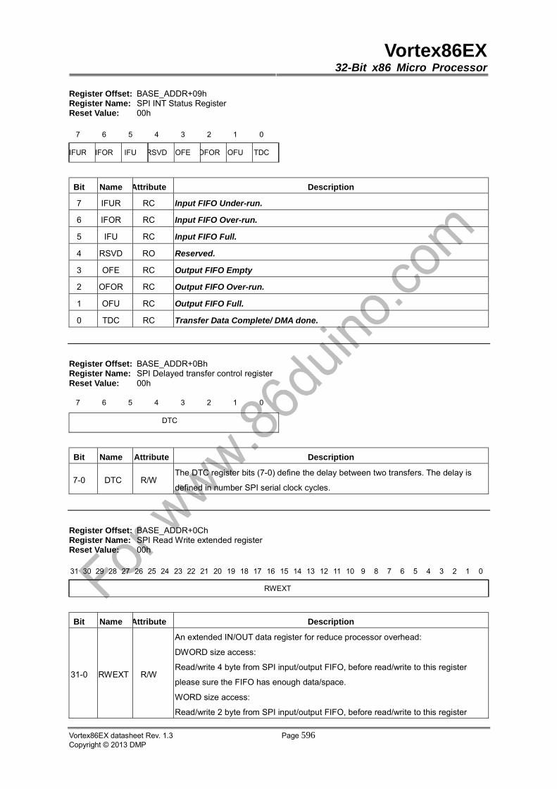
Vortex86EX32-Bit x86 Micro Processor
Vortex86EX datasheet Rev. 1.3 Page 596Copyright © 2013 DMP
Register Offset: BASE_ADDR+09h Register Name: SPI INT Status Register Reset Value: 00h
7 6 5 4 3 2 1 0
IFUR IFOR IFU RSVD OFE OFOR OFU TDC
Bit Name Attribute Description
7 IFUR RC Input FIFO Under-run.
6 IFOR RC Input FIFO Over-run.
5 IFU RC Input FIFO Full.
4 RSVD RO Reserved.
3 OFE RC Output FIFO Empty
2 OFOR RC Output FIFO Over-run.
1 OFU RC Output FIFO Full.
0 TDC RC Transfer Data Complete/ DMA done.
Register Offset: BASE_ADDR+0Bh Register Name: SPI Delayed transfer control register Reset Value: 00h
7 6 5 4 3 2 1 0
DTC
Bit Name Attribute Description
7-0 DTC R/W The DTC register bits (7-0) define the delay between two transfers. The delay is
defined in number SPI serial clock cycles.
Register Offset: BASE_ADDR+0Ch Register Name: SPI Read Write extended register Reset Value: 00h
31 30 29 28 27 26 25 24 23 22 21 20 19 18 17 16 15 14 13 12 11 10 9 8 7 6 5 4 3 2 1 0
RWEXT
Bit Name Attribute Description
31-0 RWEXT R/W
An extended IN/OUT data register for reduce processor overhead:
DWORD size access:
Read/write 4 byte from SPI input/output FIFO, before read/write to this register
please sure the FIFO has enough data/space.
WORD size access:
Read/write 2 byte from SPI input/output FIFO, before read/write to this register
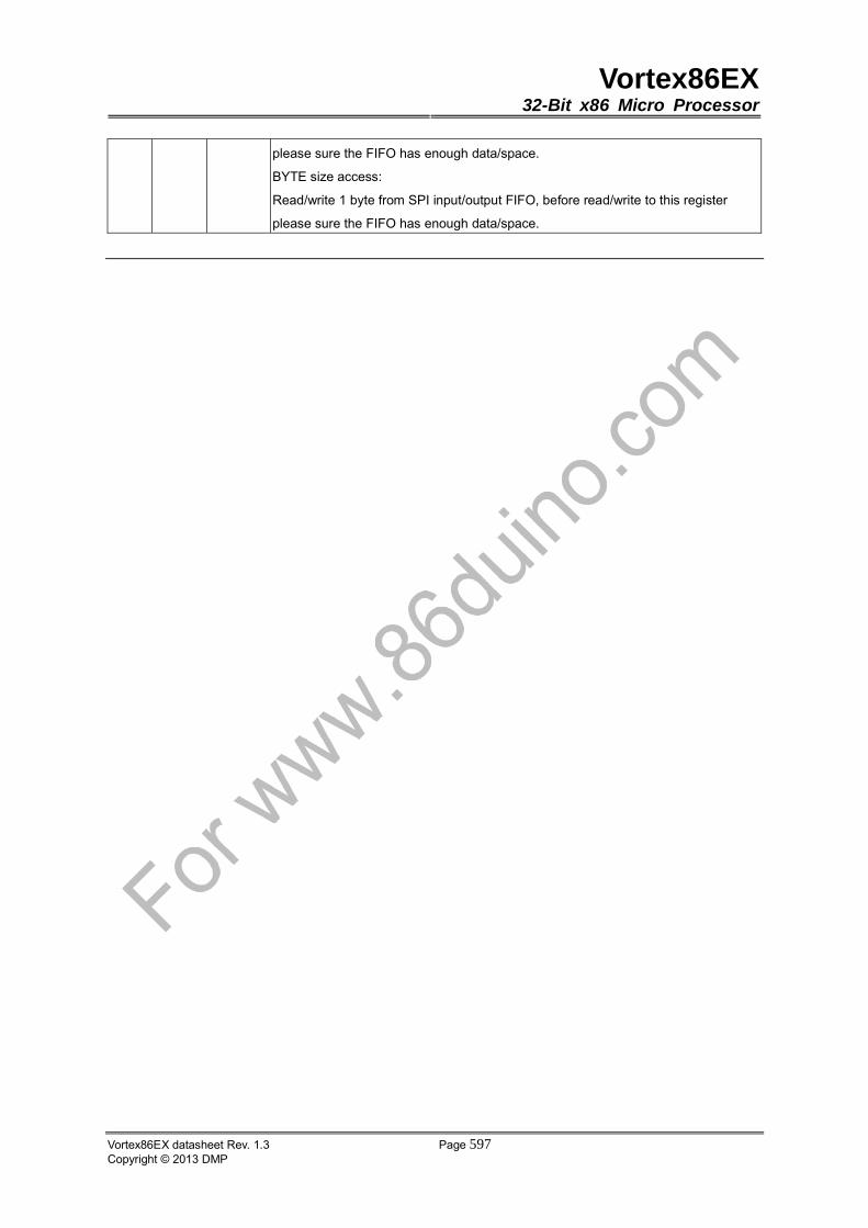
Vortex86EX32-Bit x86 Micro Processor
Vortex86EX datasheet Rev. 1.3 Page 597Copyright © 2013 DMP
please sure the FIFO has enough data/space.
BYTE size access:
Read/write 1 byte from SPI input/output FIFO, before read/write to this register
please sure the FIFO has enough data/space.

Vortex86EX32-Bit x86 Micro Processor
Vortex86EX datasheet Rev. 1.3 Page 598Copyright © 2013 DMP
21. Electrical Specifications
21.1 Performance Characteristics
Core Voltage System clock Core Frequency Max Power Typ Power
1.2V (Nominal)
25MHz 400MHz 3 Watt 2 Watt
21.2 Absolute Maximum Ratings
Symbol Parameter Min. Max. Unit Conditions
TA Ambient Temperature -40 85
Temperature of the
surrounding
medium
Tstg Storage Temperature -40 125 Dry Pack.
VDD12 SB Core power -0.3 1.26 V
DIF_VD12IO Differential PAD -0.3 1.26 V
AFE_VCCDL12Ethernet PHY Digital Logic Cell
Core -0.3 1.26 V
AVDD_USB12 USB 1.2V Power -0.3 1.26 V
AVDD_USBPLL12 USB PLL Power -0.3 1.26 V
AVDD_SATA12SATA PHY: 1.2V Analogue
Power -0.3 1.26 V
AVDD_SATARX12SATA PHY: Receiver 1.2V
Analogue Power -0.3 1.26 V
AVDD_SATAPLL12
SATA PHY: PLL 1.2V Analogue Power
-0.3 1.26 V
AVDD_PE12 PCIE 1.2V Power -0.3 1.26 V
AVDD_PERX12 PCIE Receiver 1.2V Power -0.3 1.26 V
VDD18 SB Analogue Power -0.3 1.89 V
AFE_VCCABG18Ethernet PHY Band Gap 1.8V
Power -0.3 1.89 V
AFE_VCCAPLL18 Ethernet PHY PLL 1.8V Power -0.3 1.89 V
AFE_VCCD18 Ethernet PHY 1.8V Power -0.3 1.89 V
AFE_RXVCCA18Ethernet PHY Receiver 1.8V
Power -0.3 1.89 V
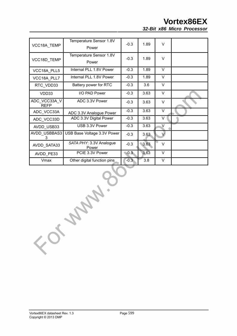
Vortex86EX32-Bit x86 Micro Processor
Vortex86EX datasheet Rev. 1.3 Page 599Copyright © 2013 DMP
VCC18A_TEMPTemperature Sensor 1.8V
Power -0.3 1.89 V
VCC18D_TEMPTemperature Sensor 1.8V
Power -0.3 1.89 V
VCC18A_PLL5 Internal PLL 1.8V Power -0.3 1.89 V
VCC18A_PLL7 Internal PLL 1.8V Power -0.3 1.89 V
RTC_VDD33 Battery power for RTC -0.3 3.6 V
VDD33 I/O PAD Power -0.3 3.63 V
ADC_VCC33A_VREFP
ADC 3.3V Power -0.3 3.63 V
ADC_VCC33A ADC 3.3V Analogue Power -0.3 3.63 V
ADC_VCC33D ADC 3.3V Digital Power -0.3 3.63 V
AVDD_USB33 USB 3.3V Power -0.3 3.63 V
AVDD_USBBAS33
USB Base Voltage 3.3V Power -0.3 3.63 V
AVDD_SATA33SATA PHY: 3.3V Analogue
Power -0.3 3.63 V
AVDD_PE33 PCIE 3.3V Power -0.3 3.63 V
Vmax Other digital function pins -0.3 3.8 V
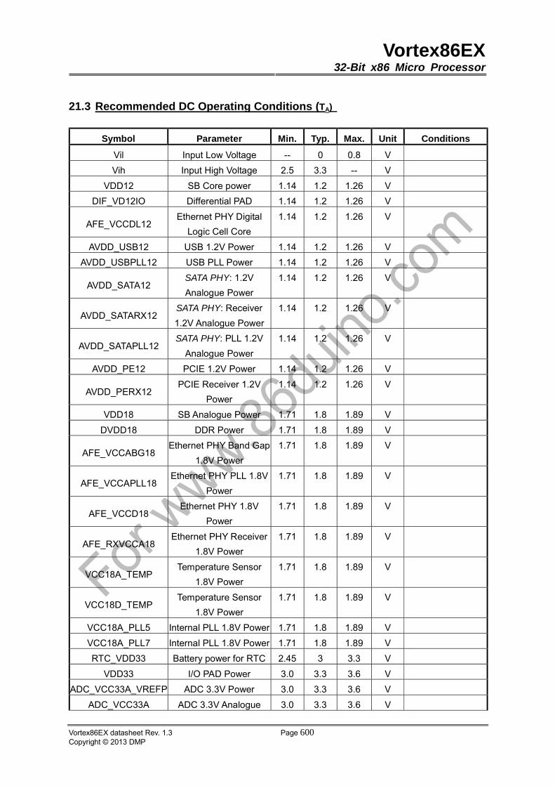
Vortex86EX32-Bit x86 Micro Processor
Vortex86EX datasheet Rev. 1.3 Page 600Copyright © 2013 DMP
21.3 Recommended DC Operating Conditions (TA)
Symbol Parameter Min. Typ. Max. Unit Conditions
Vil Input Low Voltage -- 0 0.8 V
Vih Input High Voltage 2.5 3.3 -- V
VDD12 SB Core power 1.14 1.2 1.26 V
DIF_VD12IO Differential PAD 1.14 1.2 1.26 V
AFE_VCCDL12 Ethernet PHY Digital
Logic Cell Core
1.14 1.2 1.26 V
AVDD_USB12 USB 1.2V Power 1.14 1.2 1.26 V
AVDD_USBPLL12 USB PLL Power 1.14 1.2 1.26 V
AVDD_SATA12 SATA PHY: 1.2V
Analogue Power
1.14 1.2 1.26 V
AVDD_SATARX12 SATA PHY: Receiver
1.2V Analogue Power
1.14 1.2 1.26 V
AVDD_SATAPLL12 SATA PHY: PLL 1.2V
Analogue Power
1.14 1.2 1.26 V
AVDD_PE12 PCIE 1.2V Power 1.14 1.2 1.26 V
AVDD_PERX12 PCIE Receiver 1.2V
Power
1.14 1.2 1.26 V
VDD18 SB Analogue Power 1.71 1.8 1.89 V
DVDD18 DDR Power 1.71 1.8 1.89 V
AFE_VCCABG18 Ethernet PHY Band Gap
1.8V Power
1.71 1.8 1.89 V
AFE_VCCAPLL18 Ethernet PHY PLL 1.8V
Power
1.71 1.8 1.89 V
AFE_VCCD18 Ethernet PHY 1.8V
Power
1.71 1.8 1.89 V
AFE_RXVCCA18 Ethernet PHY Receiver
1.8V Power
1.71 1.8 1.89 V
VCC18A_TEMP Temperature Sensor
1.8V Power
1.71 1.8 1.89 V
VCC18D_TEMP Temperature Sensor
1.8V Power
1.71 1.8 1.89 V
VCC18A_PLL5 Internal PLL 1.8V Power 1.71 1.8 1.89 V
VCC18A_PLL7 Internal PLL 1.8V Power 1.71 1.8 1.89 V
RTC_VDD33 Battery power for RTC 2.45 3 3.3 V
VDD33 I/O PAD Power 3.0 3.3 3.6 V
ADC_VCC33A_VREFP ADC 3.3V Power 3.0 3.3 3.6 V
ADC_VCC33A ADC 3.3V Analogue 3.0 3.3 3.6 V
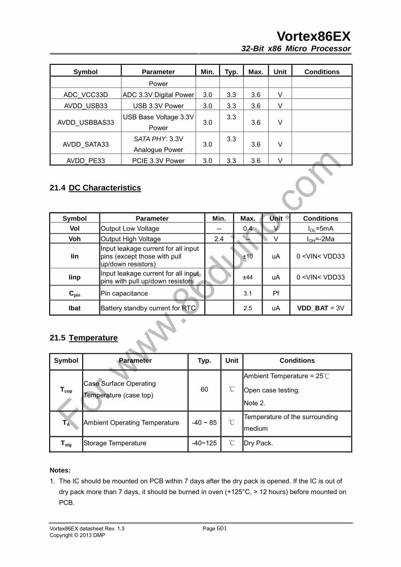
Vortex86EX32-Bit x86 Micro Processor
Vortex86EX datasheet Rev. 1.3 Page 601Copyright © 2013 DMP
Symbol Parameter Min. Typ. Max. Unit Conditions
Power
ADC_VCC33D ADC 3.3V Digital Power 3.0 3.3 3.6 V
AVDD_USB33 USB 3.3V Power 3.0 3.3 3.6 V
AVDD_USBBAS33 USB Base Voltage 3.3V
Power 3.0
3.3 3.6 V
AVDD_SATA33 SATA PHY: 3.3V
Analogue Power 3.0
3.3 3.6 V
AVDD_PE33 PCIE 3.3V Power 3.0 3.3 3.6 V
21.4 DC Characteristics
Symbol Parameter Min. Max. Unit Conditions
Vol Output Low Voltage -- 0.4 V IOL=5mA
Voh Output High Voltage 2.4 -- V IOH=-2Ma
Iin Input leakage current for all input pins (except those with pull up/down resistors)
±10 uA 0 <VIN< VDD33
Iinp Input leakage current for all input pins with pull up/down resistors
±44 uA 0 <VIN< VDD33
Cpin Pin capacitance 3.1 Pf
Ibat Battery standby current for RTC 2.5 uA VDD_BAT = 3V
21.5 Temperature
Symbol Parameter Typ. Unit Conditions
Tcop
Case Surface Operating
Temperature (case top) 60
Ambient Temperature = 25
Open case testing.
Note 2.
TA Ambient Operating Temperature -40 ~ 85Temperature of the surrounding
medium
Tstg Storage Temperature -40~125 Dry Pack.
Notes:
1. The IC should be mounted on PCB within 7 days after the dry pack is opened. If the IC is out of
dry pack more than 7 days, it should be burned in oven (+125°C, > 12 hours) before mounted on
PCB.
Vortex86EX32-Bit x86 Micro Processor
Vortex86EX datasheet Rev. 1.3 Page 602Copyright © 2013 DMP
2. Tcop depends on the number of PCB layers, PCB size, system loading, working voltage and
running pattern. The condition is for 4-layer A4-size PCB at typical working voltage.
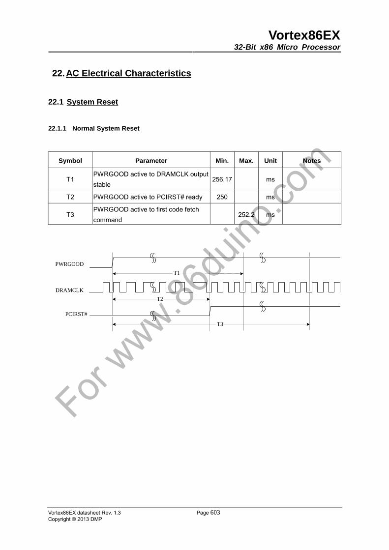
Vortex86EX32-Bit x86 Micro Processor
Vortex86EX datasheet Rev. 1.3 Page 603Copyright © 2013 DMP
22. AC Electrical Characteristics
22.1 System Reset
22.1.1 Normal System Reset
Symbol Parameter Min. Max. Unit Notes
T1 PWRGOOD active to DRAMCLK output
stable 256.17 ms
T2 PWRGOOD active to PCIRST# ready 250 ms
T3 PWRGOOD active to first code fetch
command 252.2 ms
PWRGOOD
DRAMCLK
PCIRST#
T1
T2
T3
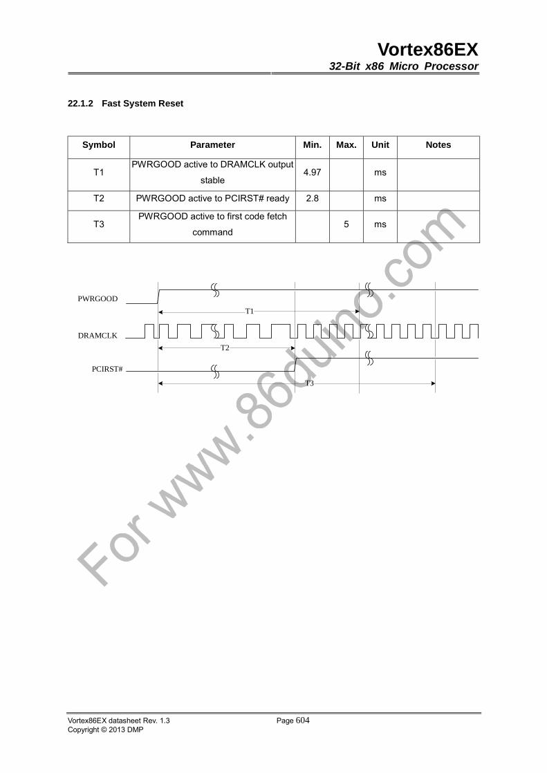
Vortex86EX32-Bit x86 Micro Processor
Vortex86EX datasheet Rev. 1.3 Page 604Copyright © 2013 DMP
22.1.2 Fast System Reset
Symbol Parameter Min. Max. Unit Notes
T1 PWRGOOD active to DRAMCLK output
stable 4.97 ms
T2 PWRGOOD active to PCIRST# ready 2.8 ms
T3 PWRGOOD active to first code fetch
command 5 ms
PWRGOOD
DRAMCLK
PCIRST#
T1
T2
T3
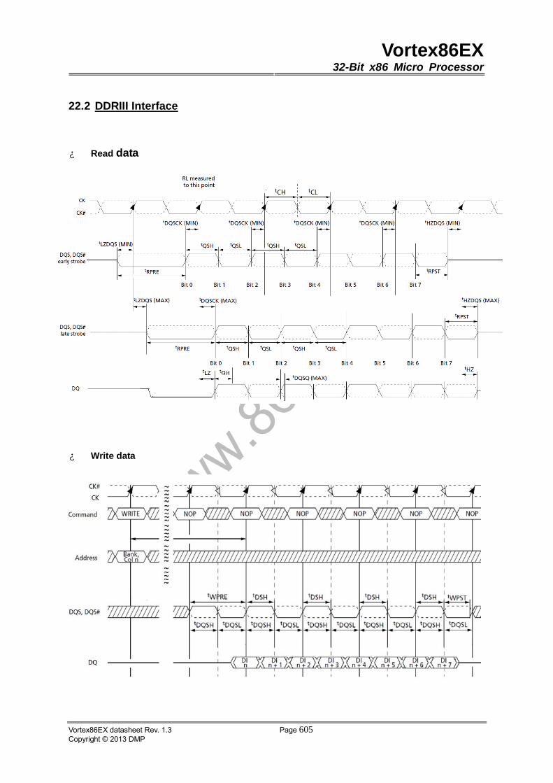
Vortex86EX32-Bit x86 Micro Processor
Vortex86EX datasheet Rev. 1.3 Page 605Copyright © 2013 DMP
22.2 DDRIII Interface
� Read data
� Write data
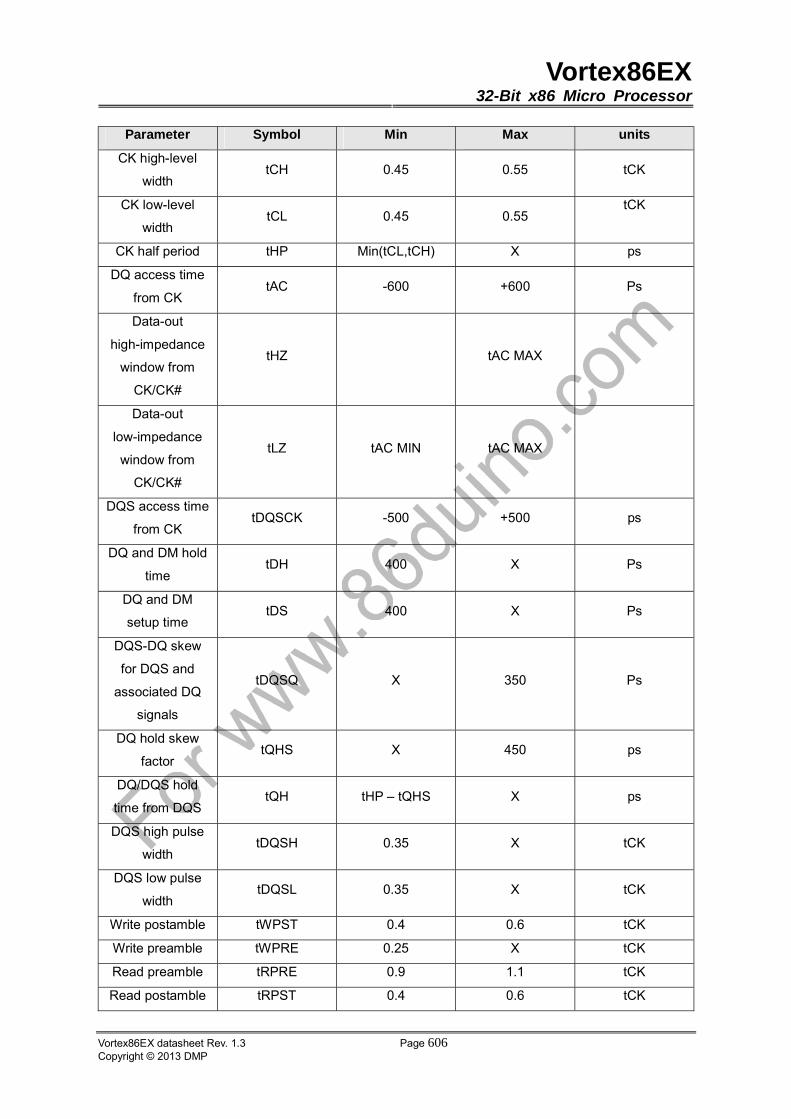
Vortex86EX32-Bit x86 Micro Processor
Vortex86EX datasheet Rev. 1.3 Page 606Copyright © 2013 DMP
Parameter Symbol Min Max units
CK high-level
width tCH 0.45 0.55 tCK
CK low-level
width tCL 0.45 0.55
tCK
CK half period tHP Min(tCL,tCH) X ps
DQ access time
from CK tAC -600 +600 Ps
Data-out
high-impedance
window from
CK/CK#
tHZ tAC MAX
Data-out
low-impedance
window from
CK/CK#
tLZ tAC MIN tAC MAX
DQS access time
from CK tDQSCK -500 +500 ps
DQ and DM hold
time tDH 400 X Ps
DQ and DM
setup time tDS 400 X Ps
DQS-DQ skew
for DQS and
associated DQ
signals
tDQSQ X 350 Ps
DQ hold skew
factor tQHS X 450 ps
DQ/DQS hold
time from DQS tQH tHP – tQHS X ps
DQS high pulse
width tDQSH 0.35 X tCK
DQS low pulse
width tDQSL 0.35 X tCK
Write postamble tWPST 0.4 0.6 tCK
Write preamble tWPRE 0.25 X tCK
Read preamble tRPRE 0.9 1.1 tCK
Read postamble tRPST 0.4 0.6 tCK
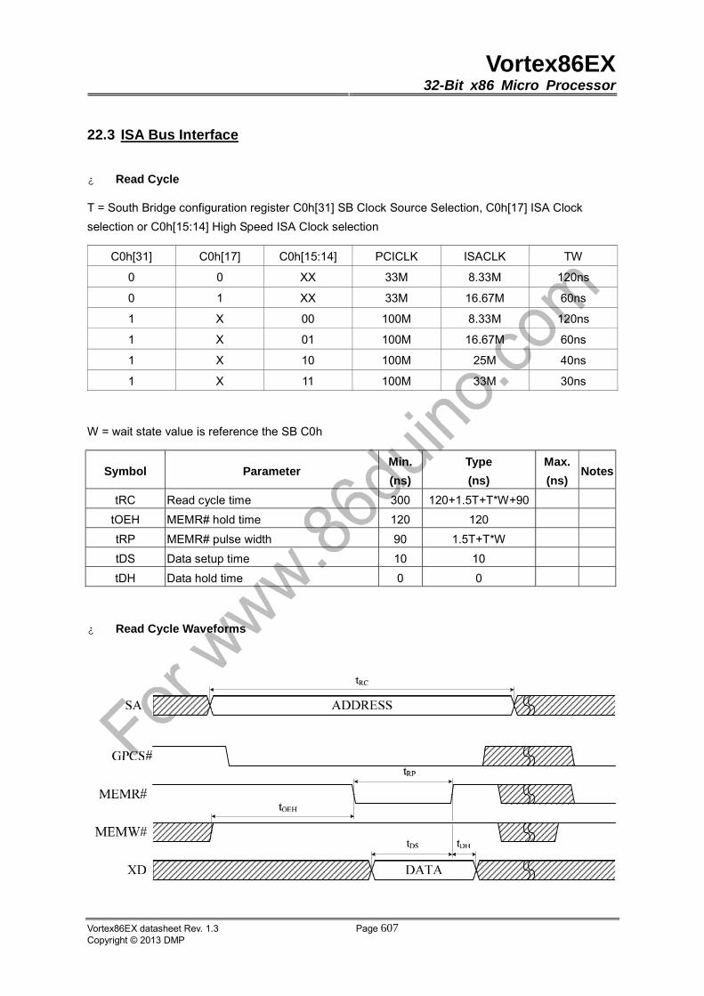
Vortex86EX32-Bit x86 Micro Processor
Vortex86EX datasheet Rev. 1.3 Page 607Copyright © 2013 DMP
22.3 ISA Bus Interface
� Read Cycle
T = South Bridge configuration register C0h[31] SB Clock Source Selection, C0h[17] ISA Clock
selection or C0h[15:14] High Speed ISA Clock selection
C0h[31] C0h[17] C0h[15:14] PCICLK ISACLK TW
0 0 XX 33M 8.33M 120ns
0 1 XX 33M 16.67M 60ns
1 X 00 100M 8.33M 120ns
1 X 01 100M 16.67M 60ns
1 X 10 100M 25M 40ns
1 X 11 100M 33M 30ns
W = wait state value is reference the SB C0h
Symbol Parameter Min.
(ns)
Type
(ns)
Max.
(ns)Notes
tRC Read cycle time 300 120+1.5T+T*W+90
tOEH MEMR# hold time 120 120
tRP MEMR# pulse width 90 1.5T+T*W
tDS Data setup time 10 10
tDH Data hold time 0 0
� Read Cycle Waveforms
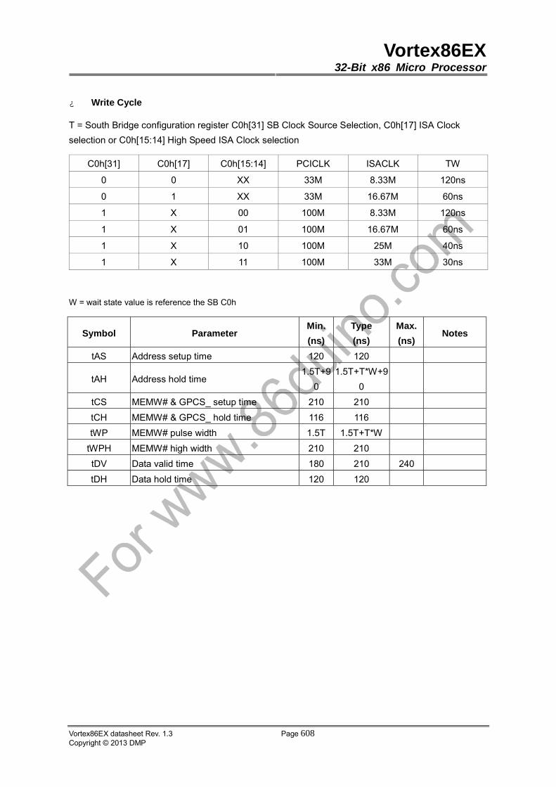
Vortex86EX32-Bit x86 Micro Processor
Vortex86EX datasheet Rev. 1.3 Page 608Copyright © 2013 DMP
� Write Cycle
T = South Bridge configuration register C0h[31] SB Clock Source Selection, C0h[17] ISA Clock
selection or C0h[15:14] High Speed ISA Clock selection
C0h[31] C0h[17] C0h[15:14] PCICLK ISACLK TW
0 0 XX 33M 8.33M 120ns
0 1 XX 33M 16.67M 60ns
1 X 00 100M 8.33M 120ns
1 X 01 100M 16.67M 60ns
1 X 10 100M 25M 40ns
1 X 11 100M 33M 30ns
W = wait state value is reference the SB C0h
Symbol Parameter Min.
(ns)
Type
(ns)
Max.
(ns)Notes
tAS Address setup time 120 120
tAH Address hold time 1.5T+9
0
1.5T+T*W+9
0
tCS MEMW# & GPCS_ setup time 210 210
tCH MEMW# & GPCS_ hold time 116 116
tWP MEMW# pulse width 1.5T 1.5T+T*W
tWPH MEMW# high width 210 210
tDV Data valid time 180 210 240
tDH Data hold time 120 120

Vortex86EX32-Bit x86 Micro Processor
Vortex86EX datasheet Rev. 1.3 Page 609Copyright © 2013 DMP
� Write Cycle Waveforms
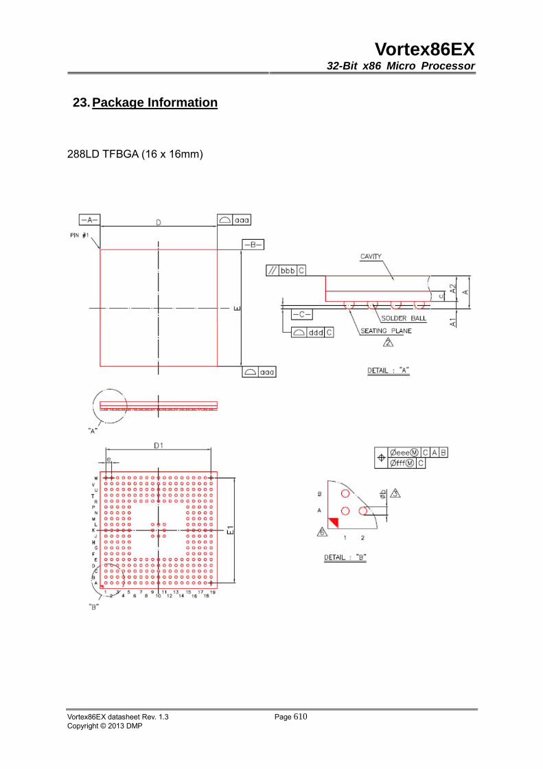
Vortex86EX32-Bit x86 Micro Processor
Vortex86EX datasheet Rev. 1.3 Page 610Copyright © 2013 DMP
23. Package Information
288LD TFBGA (16 x 16mm)

Vortex86EX32-Bit x86 Micro Processor
Vortex86EX datasheet Rev. 1.3 Page 611Copyright © 2013 DMP


![6. Wiring Diagram - weidefamily.net coil Transmission control module ... WIRING DIAGRAM 6. Wiring Diagram. MEMO: 21 WIRING DIAGRAM ... 76 6-3 [D6R2] WIRING DIAGRAM 6](https://img.pdfslide.net/doc/110x75/5aa0cc3b7f8b9a62178ea5e7/6-wiring-diagram-coil-transmission-control-module-wiring-diagram-6-wiring.jpg)