Embed Size (px)
Citation preview

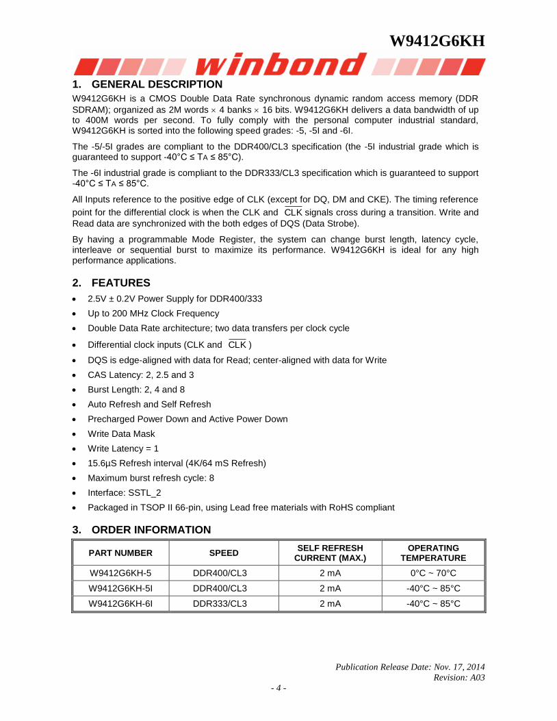
W9412G6KH
2M 4 BANKS 16 BITS DDR SDRAM
Publication Release Date: Nov. 17, 2014
Revision: A03
- 1 -
Table of Contents-
1. GENERAL DESCRIPTION ......................................................................................................... 4
2. FEATURES ................................................................................................................................. 4
3. ORDER INFORMATION ............................................................................................................. 4
4. KEY PARAMETERS ................................................................................................................... 5
5. PIN CONFIGURATION ............................................................................................................... 6
6. PIN DESCRIPTION ..................................................................................................................... 7
7. BLOCK DIAGRAM ...................................................................................................................... 8
8. FUNCTIONAL DESCRIPTION.................................................................................................... 9
8.1 Power Up Sequence ....................................................................................................... 9
8.2 Command Function ...................................................................................................... 10
8.2.1 Bank Activate Command ........................................................................... 10
8.2.2 Bank Precharge Command ........................................................................ 10
8.2.3 Precharge All Command ............................................................................ 10
8.2.4 Write Command ......................................................................................... 10
8.2.5 Write with Auto-precharge Command ........................................................ 10
8.2.6 Read Command ......................................................................................... 10
8.2.7 Read with Auto-precharge Command ....................................................... 10
8.2.8 Mode Register Set Command.................................................................... 11
8.2.9 Extended Mode Register Set Command ................................................... 11
8.2.10 No-Operation Command ............................................................................ 11
8.2.11 Burst Read Stop Command ....................................................................... 11
8.2.12 Device Deselect Command ....................................................................... 11
8.2.13 Auto Refresh Command ............................................................................ 11
8.2.14 Self Refresh Entry Command .................................................................... 12
8.2.15 Self Refresh Exit Command ....................................................................... 12
8.2.16 Data Write Enable /Disable Command ...................................................... 12
8.3 Read Operation............................................................................................................. 12
8.4 Write Operation ............................................................................................................. 13
8.5 Precharge ..................................................................................................................... 13
8.6 Burst Termination ......................................................................................................... 13
8.7 Refresh Operation ........................................................................................................ 13
8.8 Power Down Mode ....................................................................................................... 14
8.9 Input Clock Frequency Change during Precharge Power Down Mode ........................ 14
8.10 Mode Register Operation .............................................................................................. 14
8.10.1 Burst Length field (A2 to A0) ...................................................................... 14
8.10.2 Addressing Mode Select (A3) .................................................................... 15
8.10.3 CAS Latency field (A6 to A4) ..................................................................... 16
8.10.4 DLL Reset bit (A8) ..................................................................................... 16
8.10.5 Mode Register /Extended Mode register change bits (BA0, BA1)............. 16

W9412G6KH
Publication Release Date: Nov. 17, 2014
Revision: A03
- 2 -
8.10.6 Extended Mode Register field .................................................................... 16
8.10.7 Reserved field ............................................................................................ 16
9. OPERATION MODE ................................................................................................................. 17
9.1 Simplified Truth Table ................................................................................................... 17
9.2 Function Truth Table ..................................................................................................... 18
9.3 Function Truth Table for CKE ....................................................................................... 21
9.4 Simplified Stated Diagram ............................................................................................ 22
10. ELECTRICAL CHARACTERISTICS ......................................................................................... 23
10.1 Absolute Maximum Ratings .......................................................................................... 23
10.2 Recommended DC Operating Conditions .................................................................... 23
10.3 Capacitance .................................................................................................................. 24
10.4 Leakage and Output Buffer Characteristics .................................................................. 24
10.5 DC Characteristics ........................................................................................................ 25
10.6 AC Characteristics and Operating Condition ................................................................ 26
10.7 AC Test Conditions ....................................................................................................... 27
11. SYSTEM CHARACTERISTICS FOR DDR SDRAM ................................................................. 29
11.1 Table 1: Input Slew Rate for DQ, DQS, and DM .......................................................... 29
11.2 Table 2: Input Setup & Hold Time Derating for Slew Rate ........................................... 29
11.3 Table 3: Input/Output Setup & Hold Time Derating for Slew Rate ............................... 29
11.4 Table 4: Input/Output Setup & Hold Derating for Rise/Fall Delta Slew Rate ................ 29
11.5 Table 5: Output Slew Rate Characteristics (x16 Devices only) .................................... 29
11.6 Table 6: Output Slew Rate Matching Ratio Characteristics ......................................... 30
11.7 Table 7: AC Overshoot/Undershoot Specification for Address and Control Pins ......... 30
11.8 Table 8: Overshoot/Undershoot Specification for Data, Strobe, and Mask Pins .......... 31
11.9 System Notes:............................................................................................................... 32
12. TIMING WAVEFORMS ............................................................................................................. 34
12.1 Command Input Timing ................................................................................................ 34
12.2 Timing of the CLK Signals ............................................................................................ 34
12.3 Read Timing (Burst Length = 4) ................................................................................... 35
12.4 Write Timing (Burst Length = 4) .................................................................................... 36
12.5 DM, DATA MASK (W9412G6KH) ................................................................................. 37
12.6 Mode Register Set (MRS) Timing ................................................................................. 38
12.7 Extend Mode Register Set (EMRS) Timing .................................................................. 39
12.8 Auto-precharge Timing (Read Cycle, CL = 2) .............................................................. 40
12.9 Auto-precharge Timing (Read cycle, CL = 2), continued ............................................. 41
12.10 Auto-precharge Timing (Write Cycle) .......................................................................... 42
12.11 Read Interrupted by Read (CL = 2, BL = 2, 4, 8) ........................................................ 43
12.12 Burst Read Stop (BL = 8) ............................................................................................ 43
12.13 Read Interrupted by Write & BST (BL = 8) .................................................................. 44
12.14 Read Interrupted by Precharge (BL = 8) ..................................................................... 44
12.15 Write Interrupted by Write (BL = 2, 4, 8) ..................................................................... 45
12.16 Write Interrupted by Read (CL = 2, BL = 8) ................................................................ 45
12.17 Write Interrupted by Read (CL = 3, BL = 4) ................................................................ 46
12.18 Write Interrupted by Precharge (BL = 8) ..................................................................... 46
12.19 2 Bank Interleave Read Operation (CL = 2, BL = 2) ................................................... 47

W9412G6KH
Publication Release Date: Nov. 17, 2014
Revision: A03
- 3 -
12.20 2 Bank Interleave Read Operation (CL = 2, BL = 4) ................................................... 47
12.21 4 Bank Interleave Read Operation (CL = 2, BL = 2) ................................................... 48
12.22 4 Bank Interleave Read Operation (CL = 2, BL = 4) ................................................... 48
12.23 Auto Refresh Cycle ..................................................................................................... 49
12.24 Precharge/Activate Power Down Mode Entry and Exit Timing ................................... 49
12.25 Input Clock Frequency Change during Precharge Power Down Mode Timing .......... 49
12.26 Self Refresh Entry and Exit Timing ............................................................................. 50
13. PACKAGE SPECIFICATION .................................................................................................... 51
14. REVISION HISTORY ................................................................................................................ 52
W9412G6KH
Publication Release Date: Nov. 17, 2014
Revision: A03
- 4 -
1. GENERAL DESCRIPTION
W9412G6KH is a CMOS Double Data Rate synchronous dynamic random access memory (DDR
SDRAM); organized as 2M words 4 banks 16 bits. W9412G6KH delivers a data bandwidth of up to 400M words per second. To fully comply with the personal computer industrial standard, W9412G6KH is sorted into the following speed grades: -5, -5I and -6I.
The -5/-5I grades are compliant to the DDR400/CL3 specification (the -5I industrial grade which is guaranteed to support -40°C ≤ TA ≤ 85°C).
The -6I industrial grade is compliant to the DDR333/CL3 specification which is guaranteed to support -40°C ≤ TA ≤ 85°C.
All Inputs reference to the positive edge of CLK (except for DQ, DM and CKE). The timing reference
point for the differential clock is when the CLK and CLK signals cross during a transition. Write and
Read data are synchronized with the both edges of DQS (Data Strobe).
By having a programmable Mode Register, the system can change burst length, latency cycle, interleave or sequential burst to maximize its performance. W9412G6KH is ideal for any high performance applications.
2. FEATURES
2.5V ± 0.2V Power Supply for DDR400/333
Up to 200 MHz Clock Frequency
Double Data Rate architecture; two data transfers per clock cycle
Differential clock inputs (CLK and CLK )
DQS is edge-aligned with data for Read; center-aligned with data for Write
CAS Latency: 2, 2.5 and 3
Burst Length: 2, 4 and 8
Auto Refresh and Self Refresh
Precharged Power Down and Active Power Down
Write Data Mask
Write Latency = 1
15.6µS Refresh interval (4K/64 mS Refresh)
Maximum burst refresh cycle: 8
Interface: SSTL_2
Packaged in TSOP II 66-pin, using Lead free materials with RoHS compliant
3. ORDER INFORMATION
PART NUMBER SPEED SELF REFRESH
CURRENT (MAX.) OPERATING
TEMPERATURE
W9412G6KH-5 DDR400/CL3 2 mA 0°C ~ 70°C
W9412G6KH-5I DDR400/CL3 2 mA -40°C ~ 85°C
W9412G6KH-6I DDR333/CL3 2 mA -40°C ~ 85°C

W9412G6KH
Publication Release Date: Nov. 17, 2014
Revision: A03
- 5 -
4. KEY PARAMETERS
SYMBOL DESCRIPTION MIN/MAX. -5/-5I -6I
tCK Clock Cycle Time
CL = 2 Min. 7.5 nS 7.5 nS
Max. 12 nS 12 nS
CL = 2.5 Min. 6 nS 6 nS
Max. 12 nS 12 nS
CL = 3 Min. 5 nS 6 nS
Max. 12 nS 12 nS
tRAS Active to Precharge Command Period Min. 40 nS 42 nS
tRC Active to Ref/Active Command Period Min. 50 nS 54 nS
IDD0 Operating Current: One Bank Active-Precharge Max. 55 mA 50 mA
IDD1 Operating Current: One Bank Active-Read-Precharge Max. 65 mA 55 mA
IDD4R Burst Operation Current Max. 120 mA 110 mA
IDD4W Burst Operation Current Max. 115 mA 100 mA
IDD5 Auto Refresh Burst current Max. 70 mA 65 mA
IDD6 Self-Refresh Current Max. 2 mA 2 mA
W9412G6KH
Publication Release Date: Nov. 17, 2014
Revision: A03
- 6 -
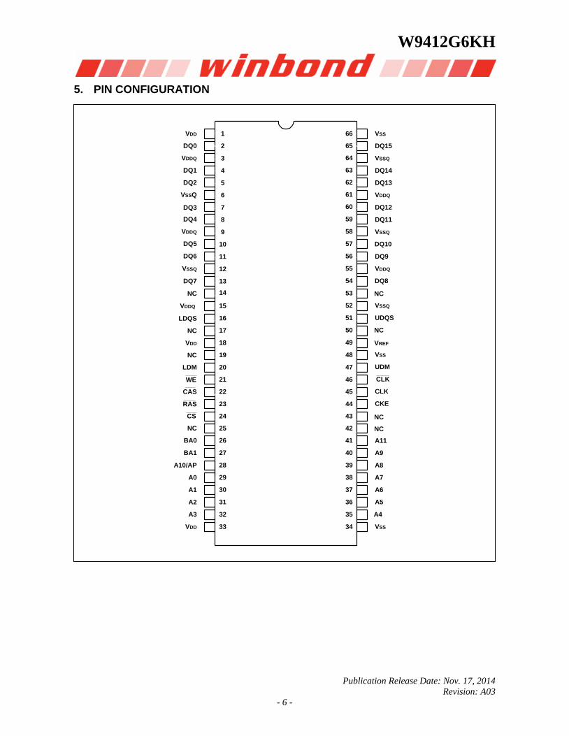
5. PIN CONFIGURATION
VSS
DQ15
VSSQ
DQ14
DQ13
VDDQ
DQ12
DQ11
VSSQ
DQ10
DQ9
VDDQ
DQ8
VSS
NC
UDQS
CLK
CKE
A11
A9
A8
A7
A6
A5
A4
VSS
66
65
64
63
62
61
60
59
58
57
56
55
54
53
52
51
50
49
48
47
46
45
44
43
42
41
40
1
2
3
4
5
6
7
8
9
10
11
12
13
14
15
16
17
18
19
20
21
22
23
24
25
26
27
VDD
DQ0
VDDQ
DQ1
DQ2
VSSQ
DQ3
DQ4
VDDQ
DQ5
DQ6
VSSQ
DQ7
NC
VDDQ
BA0
BA1
A10/AP
A0
A1
A2
A3
CS
RAS
CAS
WE
28
29
30
31
32
33
39
38
37
36
35
34VDD
LDM
NC
LDQS
NC
VDD
NC
VSSQ
NC
NC
NC
CLK
UDM
VREF

W9412G6KH
Publication Release Date: Nov. 17, 2014
Revision: A03
- 7 -
6. PIN DESCRIPTION
PIN NUMBER PIN
NAME FUNCTION DESCRIPTION
28 32,
35 41 A0 A11 Address
Multiplexed pins for row and column address.
Row address: A0 A11.Column address: A0 A8.
Provide the row address for Bank Activate commands, and the column address and Auto-precharge bit (A10) for Read/Write commands, to select one location out of the memory array in the respective bank. A10 is sampled during a precharge command to determine whether the precharge applies to one bank (A10 Low) or all banks (A10 High). If only one bank is to be precharged, the bank is selected by BA0, BA1. The address inputs also provide the op-code during a Mode Register Set command. BA0 and BA1 define which mode register is loaded during the Mode Register Set command (MRS or EMRS).
26, 27 BA0, BA1 Bank Select Select bank to activate during row address latch time, or bank to read/write during column address latch time.
2, 4, 5, 7, 8, 10, 11, 13, 54, 56, 57, 59, 60, 62, 63, 65
DQ0 DQ15
Data Input/ Output The DQ0 – DQ15 input and output data are synchronized with both edges of DQS.
16,51 LDQS, UDQS
Data Strobe DQS is Bi-directional signal. DQS is input signal during write operation and output signal during read operation. It is Edge-aligned with read data, Center-aligned with write data.
24 CS Chip Select Disable or enable the command decoder. When command decoder is disabled, new command is ignored and previous operation continues.
23, 22, 21 RAS ,
CAS , WE Command Inputs
Command inputs (along with CS ) define the command
being entered.
20, 47 LDM, UDM Write Mask When DM is asserted “high” in burst write, the input data is masked. DM is synchronized with both edges of DQS.
45, 46 CLK,
CLK
Differential Clock Inputs
All address and control input signals are sampled on the crossing of the positive edge of CLK and negative edge of
CLK .
44 CKE Clock Enable CKE controls the clock activation and deactivation. When CKE is low, Power Down mode, Suspend mode, or Self Refresh mode is entered.
49 VREF Reference Voltage VREF is reference voltage for inputs.
1, 18, 33 VDD Power Power for logic circuit inside DDR SDRAM.
34, 48, 66 VSS Ground Ground for logic circuit inside DDR SDRAM.
3, 9, 15, 55, 61 VDDQ Power for I/O
Buffer Separated power from VDD, used for output buffer, to improve noise.
6, 12, 52, 58, 64 VSSQ Ground for I/O
Buffer Separated ground from VSS, used for output buffer, to improve noise.
14, 17, 19, 25,
42, 43, 50, 53 NC No Connection No connection

W9412G6KH
Publication Release Date: Nov. 17, 2014
Revision: A03
- 8 -
7. BLOCK DIAGRAM
CKE
A10
DLL
CLOCK
BUFFER
COMMAND
DECODER
ADDRESS
BUFFER
REFRESH
COUNTER
COLUMN
COUNTER
CONTROL
SIGNAL
GENERATOR
MODE
REGISTER
COLUMN DECODER
SENSE AMPLIFIER
CELL ARRAY
BANK #2
COLUMN DECODER
SENSE AMPLIFIER
CELL ARRAY
BANK #0
COLUMN DECODER
SENSE AMPLIFIER
CELL ARRAY
BANK #3
DATA CONTROL
CIRCUIT
DQ
BUFFER
COLUMN DECODER
SENSE AMPLIFIER
CELL ARRAY
BANK #1
NOTE: The cell array configuration is 4096 * 512 * 16
RO
W D
EC
OD
ER
RO
W D
EC
OD
ER
RO
W D
EC
OD
ER
RO
W D
EC
OD
ER
A0
A9
A11
BA1BA0
CS
RAS
CAS
WE
CLK
CLK
DQ0
DQ15
PREFETCH REGISTER
LDMUDM
UDQSLDQS

W9412G6KH
Publication Release Date: Nov. 17, 2014
Revision: A03
- 9 -
8. FUNCTIONAL DESCRIPTION
8.1 Power Up Sequence
(1) Apply power and attempt to CKE at a low state (≤ 0.2V), all other inputs may be undefined
1) Apply VDD before or at the same time as VDDQ.
2) Apply VDDQ before or at the same time as VTT and VREF.
(2) Start Clock and maintain stable condition for 200 µS (min.).
(3) After stable power and clock, apply NOP and take CKE high.
(4) Issue precharge command for all banks of the device.
(5) Issue EMRS (Extended Mode Register Set) to enable DLL and establish Output Driver Type.
(6) Issue MRS (Mode Register Set) to reset DLL and set device to idle with bit A8.
(An additional 200 cycles(min) of clock are required for DLL Lock before any executable command applied.)
(7) Issue precharge command for all banks of the device.
(8) Issue two or more Auto Refresh commands.
(9) Issue MRS-Initialize device operation with the reset DLL bit deactivated A8 to low.
2 Clock min. tRFC
MRS
CLK
CommandANY
CMDAREFAREFPREAMRSEMRSPREA
CLK
tRFCtRPtRP
Enable DLL DLL reset with A8 = High Disable DLL reset with A8 = Low
200 Clock min.
2 Clock min. 2 Clock min.
Inputs
maintain stable
for 200 µS min.
Initialization sequence after power-up

W9412G6KH
Publication Release Date: Nov. 17, 2014
Revision: A03
- 10 -
8.2 Command Function
8.2.1 Bank Activate Command
(RAS = “L”, CAS = “H”, WE = “H”, BA0, BA1 = Bank, A0 to A11 = Row Address)
The Bank Activate command activates the bank designated by the BA (Bank address) signal. Row addresses are latched on A0 to A11 when this command is issued and the cell data is read out of the sense amplifiers. The maximum time that each bank can be held in the active state is specified as tRAS (max). After this command is issued, Read or Write operation can be executed.
8.2.2 Bank Precharge Command
(RAS = “L”, CAS = “H”, WE = “L”, BA0, BA1 = Bank, A10 = “L”, A0 to A9, A11 = Don’t Care)
The Bank Precharge command percharges the bank designated by BA. The precharged bank is switched from the active state to the idle state.
8.2.3 Precharge All Command
(RAS = “L”, CAS = “H”, WE = “L”, BA0, BA1 = Don’t Care, A10 = “H”, A0 to A9, A11 = Don’t
Care)
The Precharge All command precharges all banks simultaneously. Then all banks are switched to the idle state.
8.2.4 Write Command
(RAS = “H”, CAS = “L”, WE = “L”, BA0, BA1 = Bank, A10 = “L”, A0 to A8 = Column Address)
The write command performs a Write operation to the bank designated by BA. The write data are latched at both edges of DQS. The length of the write data (Burst Length) and column access sequence (Addressing Mode) must be in the Mode Register at power-up prior to the Write operation.
8.2.5 Write with Auto-precharge Command
(RAS = “H”, CAS = “L”, WE = “L”, BA0, BA1 = Bank, A10 = “H”, A0 to A8 = Column Address)
The Write with Auto-precharge command performs the Precharge operation automatically after the Write operation. This command must not be interrupted by any other commands.
8.2.6 Read Command
(RAS = “H”, CAS = “L”, WE = “H”, BA0, BA1 = Bank, A10 = “L”, A0 to A8 = Column Address)
The Read command performs a Read operation to the bank designated by BA. The read data are synchronized with both edges of DQS. The length of read data (Burst Length), Addressing Mode
and CAS Latency (access time from CAS command in a clock cycle) must be programmed in the
Mode Register at power-up prior to the Read operation.
8.2.7 Read with Auto-precharge Command
(RAS = “H”, CAS = “L”, WE = “H”, BA0, BA1 = Bank, A10 = “H”, A0 to A8 = Column Address)
The Read with Auto-precharge command automatically performs the Precharge operation after the Read operation.

W9412G6KH
Publication Release Date: Nov. 17, 2014
Revision: A03
- 11 -
1) READA ≥ tRAS (min) - (BL/2) x tCK
Internal precharge operation begins after BL/2 cycle from Read with Auto-precharge command.
2) tRCD(min) ≤ READA < tRAS(min) - (BL/2) x tCK
Data can be read with shortest latency, but the internal Precharge operation does not begin until after tRAS (min) has completed.
This command must not be interrupted by any other command.
8.2.8 Mode Register Set Command
(RAS = “L”, CAS = “L”, WE = “L”, BA0 = “L”, BA1 = “L”, A0 to A11 = Register Data)
The Mode Register Set command programs the values of CAS Latency, Addressing Mode, Burst Length and DLL reset in the Mode Register. The default values in the Mode Register after power-up are undefined, therefore this command must be issued during the power-up sequence. Also, this command can be issued while all banks are in the idle state. Refer to the table for specific codes.
8.2.9 Extended Mode Register Set Command
(RAS = “L”, CAS = “L”, WE = “L”, BA0 = “H”, BA1 = “L”, A0 to A11 = Register data)
The Extended Mode Register Set command can be implemented as needed for function extensions to the standard (SDR-SDRAM). Currently the only available mode in EMRS is DLL enable/disable, decoded by A0. The default value of the extended mode register is not defined; therefore this command must be issued during the power-up sequence for enabling DLL. Refer to the table for specific codes.
8.2.10 No-Operation Command
(RAS = “H”, CAS = “H”, WE = “H”)
The No-Operation command simply performs no operation (same command as Device Deselect).
8.2.11 Burst Read Stop Command
(RAS = “H”, CAS = “H”, WE = “L”)
The Burst stop command is used to stop the burst operation. This command is only valid during a Burst Read operation.
8.2.12 Device Deselect Command
( CS = “H”)
The Device Deselect command disables the command decoder so that the RAS , CAS , WE
and Address inputs are ignored. This command is similar to the No-Operation command.
8.2.13 Auto Refresh Command
(RAS = “L”, CAS = “L”, WE = “H”, CKE = “H”, BA0, BA1, A0 to A11 = Don’t Care)
AUTO REFRESH is used during normal operation of the DDR SDRAM and is analogous to CAS–BEFORE–RAS (CBR) refresh in previous DRAM types. This command is non persistent, so it must be issued each time a refresh is required.
The refresh addressing is generated by the internal refresh controller. This makes the address bits “Don’t Care” during an AUTO REFRESH command. The DDR SDRAM requires AUTO REFRESH cycles at an average periodic interval of tREFI (maximum).

W9412G6KH
Publication Release Date: Nov. 17, 2014
Revision: A03
- 12 -
To allow for improved efficiency in scheduling and switching between tasks, some flexibility in the absolute refresh interval is provided. A maximum of eight AUTO REFRESH commands can be posted to any given DDR SDRAM, and the maximum absolute interval between any AUTO REFRESH command and the next AUTO REFRESH command is 8 * tREFI.
8.2.14 Self Refresh Entry Command
(RAS = “L”, CAS = “L”, WE = “H”, CKE = “L”, BA0, BA1, A0 to A11 = Don’t Care)
The SELF REFRESH command can be used to retain data in the DDR SDRAM, even if the rest of the system is powered down. When in the self refresh mode, the DDR SDRAM retains data without external clocking. The SELF REFRESH command is initiated like an AUTO REFRESH command except CKE is disabled (LOW). The DLL is automatically disabled upon entering SELF REFRESH, and is automatically enabled upon exiting SELF REFRESH. Any time the DLL is enabled a DLL Reset must follow and 200 clock cycles should occur before a READ command can be issued. Input signals except CKE are “Don’t Care” during SELF REFRESH. Since CKE is an SSTL_2 input, VREF must be maintained during SELF REFRESH.
8.2.15 Self Refresh Exit Command
(CKE = “H”, CS = “H” or CKE = “H”, RAS = “H”, CAS = “H”)
The procedure for exiting self refresh requires a sequence of commands. First, CLK must be stable prior to CKE going back HIGH. Once CKE is HIGH, the DDR SDRAM must have NOP commands issued for tXSNR because time is required for the completion of any internal refresh in progress. A simple algorithm for meeting both refresh and DLL requirements is to apply NOPs for 200 clock cycles before applying any other command.
The use of SELF REFREH mode introduces the possibility that an internally timed event can be missed when CKE is raised for exit from self refresh mode. Upon exit from SELF REFRESH an extra auto refresh command is recommended.
8.2.16 Data Write Enable /Disable Command
(DM = “L/H” or LDM, UDM = “L/H”)
During a Write cycle, the DM or LDM, UDM signal functions as Data Mask and can control every word of the input data. The LDM signal controls DQ0 to DQ7 and UDM signal controls DQ8 to DQ15.
8.3 Read Operation
Issuing the Bank Activate command to the idle bank puts it into the active state. When the Read command is issued after tRCD from the Bank Activate command, the data is read out sequentially, synchronized with both edges of DQS (Burst Read operation). The initial read data becomes available after CAS Latency from the issuing of the Read command. The CAS Latency must be set in the Mode Register at power-up.
When the Precharge Operation is performed on a bank during a Burst Read and operation, the Burst operation is terminated.
When the Read with Auto-precharge command is issued, the Precharge operation is performed automatically after the Read cycle then the bank is switched to the idle state. This command cannot be interrupted by any other commands. Refer to the diagrams for Read operation.
W9412G6KH
Publication Release Date: Nov. 17, 2014
Revision: A03
- 13 -
8.4 Write Operation
Issuing the Write command after tRCD from the bank activate command. The input data is latched sequentially, synchronizing with both edges(rising & falling) of DQS after the Write command (Burst write operation). The burst length of the Write data (Burst Length) and Addressing Mode must be set in the Mode Register at power-up.
When the Precharge operation is performed in a bank during a Burst Write operation, the Burst operation is terminated.
When the Write with Auto-precharge command is issued, the Precharge operation is performed automatically after the Write cycle, then the bank is switched to the idle state, The Write with Auto-precharge command cannot be interrupted by any other command for the entire burst data duration.
Refer to the diagrams for Write operation.
8.5 Precharge
There are two Commands, which perform the precharge operation (Bank Precharge and Precharge All). When the Bank Precharge command is issued to the active bank, the bank is precharged and then switched to the idle state. The Bank Precharge command can precharge one bank independently of the other bank and hold the unprecharged bank in the active state. The maximum time each bank can be held in the active state is specified as tRAS (max). Therefore, each bank must be precharged within tRAS(max) from the bank activate command.
The Precharge All command can be used to precharge all banks simultaneously. Even if banks are not in the active state, the Precharge All command can still be issued. In this case, the Precharge operation is performed only for the active bank and the precharge bank is then switched to the idle state.
8.6 Burst Termination
When the Precharge command is used for a bank in a Burst cycle, the Burst operation is terminated. When Burst Read cycle is interrupted by the Precharge command, read operation is disabled after clock cycle of (CAS Latency) from the Precharge command. When the Burst Write cycle is interrupted by the Precharge command, the input circuit is reset at the same clock cycle at which the precharge command is issued. In this case, the DM signal must be asserted “high” during tWR to prevent writing the invalided data to the cell array.
When the Burst Read Stop command is issued for the bank in a Burst Read cycle, the Burst Read operation is terminated. The Burst read Stop command is not supported during a write burst operation. Refer to the diagrams for Burst termination.
8.7 Refresh Operation
Two types of Refresh operation can be performed on the device: Auto Refresh and Self Refresh. By repeating the Auto Refresh cycle, each bank in turn refreshed automatically. The Refresh operation must be performed 4096 times (rows) within 64mS. The period between the Auto Refresh command and the next command is specified by tRFC.
Self Refresh mode enters issuing the Self Refresh command (CKE asserted “low”) while all banks are in the idle state. The device is in Self Refresh mode for as long as CKE held “low”. In the case of distributed Auto Refresh commands, distributed auto refresh commands must be issued every 15.6 µS and the last distributed Auto Refresh commands must be performed within 15.6 µS before entering the self refresh mode. After exiting from the Self Refresh mode, the refresh operation must be performed within 15.6 µS. In Self Refresh mode, all input/output buffers are disabled, resulting in lower power dissipation (except CKE buffer). Refer to the diagrams for Refresh operation.

W9412G6KH
Publication Release Date: Nov. 17, 2014
Revision: A03
- 14 -
8.8 Power Down Mode
Two types of Power Down Mode can be performed on the device: Active Standby Power Down Mode and Precharge Standby Power Down Mode.
When the device enters the Power Down Mode, all input/output buffers are disabled resulting in low power dissipation (except CKE buffer).
Power Down Mode enter asserting CKE “low” while the device is not running a burst cycle. Taking CKE “high” can exit this mode. When CKE goes high, a No operation command must be input at next CLK rising edge. Refer to the diagrams for Power Down Mode.
8.9 Input Clock Frequency Change during Precharge Power Down Mode
DDR SDRAM input clock frequency can be changed under following condition:
DDR SDRAM must be in precharged power down mode with CKE at logic LOW level. After a minimum of 2 clocks after CKE goes LOW, the clock frequency may change to any frequency between minimum and maximum operating frequency specified for the particular speed grade. During an input clock frequency change, CKE must be held LOW. Once the input clock frequency is changed, a stable clock must be provided to DRAM before precharge power down mode may be exited. The DLL must be RESET via EMRS after precharge power down exit. An additional MRS command may need to be issued to appropriately set CL etc. After the DLL relock time, the DRAM is ready to operate with new clock frequency.
8.10 Mode Register Operation
The mode register is programmed by the Mode Register Set command (MRS/EMRS) when all banks are in the idle state. The data to be set in the Mode Register is transferred using the A0 to A11 and BA0, BA1 address inputs.
The Mode Register designates the operation mode for the read or write cycle. The register is divided into five filed: (1) Burst Length field to set the length of burst data (2) Addressing Mode selected bit to designate the column access sequence in a Burst cycle (3) CAS Latency field to set the assess time in clock cycle (4) DLL reset field to reset the DLL (5) Regular/Extended Mode Register filed to select a type of MRS (Regular/Extended MRS). EMRS cycle can be implemented the extended function (DLL enable/Disable mode).
The initial value of the Mode Register (including EMRS) after power up is undefined; therefore the Mode Register Set command must be issued before power operation.
8.10.1 Burst Length field (A2 to A0)
This field specifies the data length for column access using the A2 to A0 pins and sets the Burst Length to be 2, 4 and 8 words.
A2 A1 A0 BURST LENGTH
0 0 0 Reserved
0 0 1 2 words
0 1 0 4 words
0 1 1 8 words
1 x x Reserved

W9412G6KH
Publication Release Date: Nov. 17, 2014
Revision: A03
- 15 -
8.10.2 Addressing Mode Select (A3)
The Addressing Mode can be one of two modes; Interleave mode or Sequential Mode, When the A3 bit is “0”, Sequential mode is selected. When the A3 bit is “1”, Interleave mode is selected. Both addressing Mode support burst length 2, 4 and 8 words.
A3 ADDRESSING MODE
0 Sequential
1 Interleave
8.10.2.1. Addressing Sequence of Sequential Mode
A column access is performed by incrementing the column address input to the device. The address is varied by the Burst Length as the following.
Addressing Sequence of Sequential Mode
DATA ACCESS ADDRESS BURST LENGTH
Data 0 n 2 words (address bits is A0)
Data 1 n + 1 not carried from A0 to A1
Data 2 n + 2 4 words (address bit A0, A1)
Data 3 n + 3 Not carried from A1 to A2
Data 4 n + 4
Data 5 n + 5 8 words (address bits A2, A1 and A0)
Data 6 n + 6 Not carried from A2 to A3
Data 7 n + 7
8.10.2.2. Addressing Sequence for Interleave Mode
A Column access is started from the inputted column address and is performed by interleaving the address bits in the sequence shown as the following.
Addressing Sequence of Interleave Mode
DATA ACCESS ADDRESS BURST LENGTH
Data 0 A8 A7 A6 A5 A4 A3 A2 A1 A0 2 words
Data 1 A8 A7 A6 A5 A4 A3 A2 A1 A0
Data 2 A8 A7 A6 A5 A4 A3 A2 A1 A0 4 words
Data 3 A8 A7 A6 A5 A4 A3 A2 A1 A0
Data 4 A8 A7 A6 A5 A4 A3 A2 A1 A0 8 words
Data 5 A8 A7 A6 A5 A4 A3 A2 A1 A0
Data 6 A8 A7 A6 A5 A4 A3 A2 A1 A0
Data 7 A8 A7 A6 A5 A4 A3 A2 A1 A0

W9412G6KH
Publication Release Date: Nov. 17, 2014
Revision: A03
- 16 -
8.10.3 CAS Latency field (A6 to A4)
This field specifies the number of clock cycles from the assertion of the Read command to the first data read. The minimum values of CAS Latency depend on the frequency of CLK.
A6 A5 A4 CAS LATENCY
0 0 0 Reserved
0 0 1 Reserved
0 1 0 2
0 1 1 3
1 0 0 Reserved
1 0 1 Reserved
1 1 0 2.5
1 1 1 Reserved
8.10.4 DLL Reset bit (A8)
This bit is used to reset DLL. When the A8 bit is “1”, DLL is reset.
8.10.5 Mode Register /Extended Mode register change bits (BA0, BA1)
These bits are used to select MRS/EMRS.
BA1 BA0 A11-A0
0 0 Regular MRS Cycle
0 1 Extended MRS Cycle
1 x Reserved
8.10.6 Extended Mode Register field
1) DLL Switch field (A0)
This bit is used to select DLL enable or disable
A0 DLL
0 Enable
1 Disable
2) Output Driver Strength Control field (A6, A1)
The 100%, 60% and 30% or matched impedance driver strength are required Extended Mode Register Set (EMRS) as the following:
A6 A1 BUFFER STRENGTH
0 0 100% Strength
0 1 60% Strength
1 0 Reserved
1 1 30% Strength
8.10.7 Reserved field
Test mode entry bit (A7)
This bit is used to enter Test mode and must be set to “0” for normal operation.
Reserved bits (A9, A10, A11) These bits are reserved for future operations. They must be set to “0” for normal operation.

W9412G6KH
Publication Release Date: Nov. 17, 2014
Revision: A03
- 17 -
9. OPERATION MODE
The following table shows the operation commands.
9.1 Simplified Truth Table
SYM. COMMAND DEVICE STATE
CKEn-1 CKEn DM(4) BA0,BA1
A10 A0-A9 ,A11 CS RAS CAS W E
ACT Bank Active Idle(3) H X X V V V L L H H
PRE Bank Precharge Any(3) H X X V L X L L H L
PREA Precharge All Any H X X X H X L L H L
WRIT Write Active(3) H X X V L V L H L L
WRITA Write with Auto-precharge
Active(3) H X X V H V L H L L
READ Read Active(3) H X X V L V L H L H
READA Read with Auto-precharge
Active(3) H X X V H V L H L H
MRS Mode Register Set Idle H X X L, L
Op-Code(6)
L L L L
EMRS Extended Mode Register Set
Idle H X X H, L L L L L
NOP No Operation Any H X X X X X L H H H
BST Burst Read Stop Active H X X X X X L H H L
DSL Device Deselect Any H X X X X X H X X X
AREF Auto Refresh Idle H H X X X X L L L H
SELF Self Refresh Entry
Idle H L X X X X L L L H
SELEX Self Refresh Exit Idle (Self Refresh)
L H X X X X H X X X
L H H X
PD Power Down Mode Entry
Idle/ Active(5) H L X X X X
H X X X
L H H X
PDEX Power Down Mode Exit
Any (Power Down)
L H X X X X H X X X
L H H X
WDE Data Write Enable Active H X L X X X X X X X
WDD Data Write Disable Active H X H X X X X X X X
Notes
1. V = Valid X = Don’t Care L = Low level H = High level.
2. CKEn signal is input level when commands are issued
CKEn-1 signal is input level one clock cycle before the commands are issued
3. These are state designated by the BA0, BA1 signals.
4. LDM, UDM (W9412G6KH)
5. Power Down Mode can not entry in the burst cycle.
6. BA0, BA1 select either the Base or the Extended Mode Register (BA0 = 0, BA1 = 0 selects Mode Register; BA0 = 1, BA1 = 0 selects Extended Mode Register; other combinations of BA0, BA1 are reserved; A0~A11 provide the op-code to be written to the selected Mode Register (MRS or EMRS).

W9412G6KH
Publication Release Date: Nov. 17, 2014
Revision: A03
- 18 -
9.2 Function Truth Table (Note 1)
CURRENT STATE CS RAS CAS W E ADDRESS COMMAND ACTION NOTES
Idle
H X X X X DSL NOP
L H H X X NOP/BST NOP
L H L H BA, CA, A10 READ/READA ILLEGAL 3
L H L L BA, CA, A10 WRIT/WRITA ILLEGAL 3
L L H H BA, RA ACT Row activating
L L H L BA, A10 PRE/PREA NOP
L L L H X AREF/SELF Refresh or Self refresh 2
L L L L Op-Code MRS/EMRS Mode register accessing 2
Row Active
H X X X X DSL NOP
L H H X X NOP/BST NOP
L H L H BA, CA, A10 READ/READA Begin read: Determine AP 4
L H L L BA, CA, A10 WRIT/WRITA Begin write: Determine AP 4
L L H H BA, RA ACT ILLEGAL 3
L L H L BA, A10 PRE/PREA Precharge 5
L L L H X AREF/SELF ILLEGAL
L L L L Op-Code MRS/EMRS ILLEGAL
Read
H X X X X DSL Continue burst to end
L H H H X NOP Continue burst to end
L H H L X BST Burst stop
L H L H BA, CA, A10 READ/READA Term burst, new read: Determine AP 6
L H L L BA, CA, A10 WRIT/WRITA ILLEGAL
L L H H BA, RA ACT ILLEGAL 3
L L H L BA, A10 PRE/PREA Term burst, precharging
L L L H X AREF/SELF ILLEGAL
L L L L Op-Code MRS/EMRS ILLEGAL
Write
H X X X X DSL Continue burst to end
L H H H X NOP Continue burst to end
L H H L X BST ILLEGAL
L H L H BA, CA, A10 READ/READA Term burst, start read: Determine AP 6, 7
L H L L BA, CA, A10 WRIT/WRITA Term burst, start read: Determine AP 6
L L H H BA, RA ACT ILLEGAL 3
L L H L BA, A10 PRE/PREA Term burst, precharging 8
L L L H X AREF/SELF ILLEGAL
L L L L Op-Code MRS/EMRS ILLEGAL

W9412G6KH
Publication Release Date: Nov. 17, 2014
Revision: A03
- 19 -
Function Truth Table, continued
CURRENT STATE CS RAS CAS W E ADDRESS COMMAND ACTION NOTES
Read with Auto-
precharge
H X X X X DSL Continue burst to end
L H H H X NOP Continue burst to end
L H H L X BST ILLEGAL
L H L H BA, CA, A10 READ/READA ILLEGAL
L H L L BA, CA, A10 WRIT/WRITA ILLEGAL 3
L L H H BA, RA ACT ILLEGAL 3
L L H L BA, A10 PRE/PREA ILLEGAL
L L L H X AREF/SELF ILLEGAL
L L L L Op-Code MRS/EMRS ILLEGAL
Write with Auto-
precharge
H X X X X DSL Continue burst to end
L H H H X NOP Continue burst to end
L H H L X BST ILLEGAL
L H L H BA, CA, A10 READ/READA ILLEGAL
L H L L BA, CA, A10 WRIT/WRITA ILLEGAL
L L H H BA, RA ACT ILLEGAL 3
L L H L BA, A10 PRE/PREA ILLEGAL 3
L L L H X AREF/SELF ILLEGAL
L L L L Op-Code MRS/EMRS ILLEGAL
Precharging
H X X X X DSL NOP-> Idle after tRP
L H H H X NOP NOP-> Idle after tRP
L H H L X BST ILLEGAL
L H L H BA, CA, A10 READ/READA ILLEGAL 3
L H L L BA, CA, A10 WRIT/WRITA ILLEGAL 3
L L H H BA, RA ACT ILLEGAL 3
L L H L BA, A10 PRE/PREA Idle after tRP
L L L H X AREF/SELF ILLEGAL
L L L L Op-Code MRS/EMRS ILLEGAL
Row Activating
H X X X X DSL NOP-> Row active after tRCD
L H H H X NOP NOP-> Row active after tRCD
L H H L X BST ILLEGAL
L H L H BA, CA, A10 READ/READA ILLEGAL 3
L H L L BA, CA, A10 WRIT/WRITA ILLEGAL 3
L L H H BA, RA ACT ILLEGAL 3
L L H L BA, A10 PRE/PREA ILLEGAL 3
L L L H X AREF/SELF ILLEGAL
L L L L Op-Code MRS/EMRS ILLEGAL

W9412G6KH
Publication Release Date: Nov. 17, 2014
Revision: A03
- 20 -
Function Truth Table, continued
CURRENT STATE CS RAS CAS W E ADDRESS COMMAND ACTION NOTES
Write
Recovering
H X X X X DSL NOP->Row active after tWR
L H H H X NOP NOP->Row active after tWR
L H H L X BST ILLEGAL
L H L H BA, CA, A10 READ/READA ILLEGAL 3
L H L L BA, CA, A10 WRIT/WRITA ILLEGAL 3
L L H H BA, RA ACT ILLEGAL 3
L L H L BA, A10 PRE/PREA ILLEGAL 3
L L L H X AREF/SELF ILLEGAL
L L L L Op-Code MRS/EMRS ILLEGAL
Write Recovering with Auto-precharge
H X X X X DSL NOP->Enter precharge after tWR
L H H H X NOP NOP->Enter precharge after tWR
L H H L X BST ILLEGAL
L H L H BA, CA, A10 READ/READA ILLEGAL 3
L H L L BA, CA, A10 WRIT/WRITA ILLEGAL 3
L L H H BA, RA ACT ILLEGAL 3
L L H L BA, A10 PRE/PREA ILLEGAL 3
L L L H X AREF/SELF ILLEGAL
L L L L Op-Code MRS/EMRS ILLEGAL
Refreshing
H X X X X DSL NOP->Idle after tRC
L H H H X NOP NOP->Idle after tRC
L H H L X BST ILLEGAL
L H L H X READ/WRIT ILLEGAL
L L H X X ACT/PRE/PREA ILLEGAL
L L L X X AREF/SELF/MRS/EMRS ILLEGAL
Mode Register
Accessing
H X X X X DSL NOP->Row after tMRD
L H H H X NOP NOP->Row after tMRD
L H H L X BST ILLEGAL
L H L X X READ/WRIT ILLEGAL
L L X X X ACT/PRE/PREA/AREF/SELF/MRS/EMRS
ILLEGAL
Notes
1. All entries assume that CKE was active (High level) during the preceding clock cycle and the current clock cycle.
2. Illegal if any bank is not idle.
3. Illegal to bank in specified states; Function may be legal in the bank indicated by Bank Address (BA), depending on the state of that bank.
4. Illegal if tRCD is not satisfied.
5. Illegal if tRAS is not satisfied.
6. Must satisfy burst interrupt condition.
7. Must avoid bus contention, bus turn around, and/or satisfy write recovery requirements.
8. Must mask preceding data which don’t satisfy tWR
Remark: H = High level, L = Low level, X = High or Low level (Don’t Care), V = Valid data

W9412G6KH
Publication Release Date: Nov. 17, 2014
Revision: A03
- 21 -
9.3 Function Truth Table for CKE
CURRENT STATE
CKE CS RAS CAS W E ADDRESS ACTION NOTES
n-1 n
Self Refresh
H X X X X X X INVALID
L H H X X X X Exit Self Refresh->Idle after tXSNR
L H L H H X X Exit Self Refresh->Idle after tXSNR
L H L H L X X ILLEGAL
L H L L X X X ILLEGAL
L L X X X X X Maintain Self Refresh
Power Down
H X X X X X X INVALID
L H X X X X X Exit Power down->Idle after tIS
L L X X X X X Maintain power down mode
All banks Idle
H H X X X X X Refer to Function Truth Table
H L H X X X X Enter Power down 2
H L L H H X X Enter Power down 2
H L L L L H X Self Refresh 1
H L L H L X X ILLEGAL
H L L L X X X ILLEGAL
L X X X X X X Power down
Row Active
H H X X X X X Refer to Function Truth Table
H L H X X X X Enter Power down 3
H L L H H X X Enter Power down 3
H L L L L H X ILLEGAL
H L L H L X X ILLEGAL
H L L L X X X ILLEGAL
L X X X X X X Power down
Any State Other Than
Listed Above H H X X X X X Refer to Function Truth Table
Notes
1. Self refresh can enter only from the all banks idle state.
2. Power Down occurs when all banks are idle; this mode is referred to as precharge power down.
3. Power Down occurs when there is a row active in any bank; this mode is referred to as active power down.
Remark: H = High level, L = Low level, X = High or Low level (Don’t Care), V = Valid data

W9412G6KH
Publication Release Date: Nov. 17, 2014
Revision: A03
- 22 -
9.4 Simplified Stated Diagram
POWER
APPLIED
Automatic Sequence
Command Sequence
Read A
Write Read
ROW
ACTIVE
POWER
DOWN
IDLE
MODE
REGISTER
SET
AUTO
REFRESH
SELF
REFRESH
Read
Read A
Write
Write A
PRE
CHARGE
POWER
ON
MRS/EMRS
AREF
SREF
SREFX
PD
PDEX
ACT
BST
ReadWrite
Write A
Write A Read A
PRE
PRE
PRE
PRE
ACTIVE
POWERDOWN
PD
PDEX
Read
Read A

W9412G6KH
Publication Release Date: Nov. 17, 2014
Revision: A03
- 23 -
10. ELECTRICAL CHARACTERISTICS
10.1 Absolute Maximum Ratings
PARAMETER SYMBOL RATING UNIT
Voltage on I/O Pins Relative to VSS VIN, VOUT -0.5 ~ VDDQ +0.5 V
Voltage on Input Pins Relative to VSS VIN -1 ~ 3.6 V
Voltage on VDD Supply Relative to VSS VDD -1 ~ 3.6 V
Voltage on VDDQ Supply Relative to VSS VDDQ -1 ~ 3.6 V
Operating Temperature (-5) TOPR 0 ~ 70 °C
Operating Temperature (-5I/-6I) TOPR -40 ~ 85 °C
Storage Temperature TSTG -55 ~ 150 °C
Soldering Temperature (10s) TSOLDER 260 °C
Power Dissipation PD 1 W
Short Circuit Output Current IOUT 50 mA
Note: Stresses greater than those listed under “Absolute Maximum Ratings” may cause permanent damage to the device.
This is a stress rating only, and functional operation of the device at these or any other conditions above those indicated in the operational sections of this specification is not implied.
Exposure to absolute maximum rating conditions for extended periods may affect reliability.
10.2 Recommended DC Operating Conditions (TA = 0 to 70°C for -5, TA = -40 to 85°C for -5I/-6I)
SYM. PARAMETER MIN. TYP. MAX. UNIT NOTES
VDD Power Supply Voltage (for -5/-5I/-6I) 2.3 2.5 2.7 V 2
VDDQ I/O Buffer Supply Voltage (for -5/-5I/-6I) 2.3 2.5 2.7 V 2
VREF Input reference Voltage 0.49 x VDDQ 0.50 x VDDQ 0.51 x VDDQ V 2, 3
VTT Termination Voltage (System) VREF - 0.04 VREF VREF + 0.04 V 2, 8
VIH (DC) Input High Voltage (DC) VREF + 0.15 - VDDQ + 0.3 V 2
VIL (DC) Input Low Voltage (DC) -0.3 - VREF - 0.15 V 2
VICK (DC) Differential Clock DC Input Voltage -0.3 - VDDQ + 0.3 V 15
VID (DC) Input Differential Voltage.
CLK and CLK inputs (DC) 0.36 - VDDQ + 0.6 V 13, 15
VIH (AC) Input High Voltage (AC) VREF + 0.31 - - V 2
VIL (AC) Input Low Voltage (AC) - - VREF - 0.31 V 2
VID (AC) Input Differential Voltage.
CLK and CLK inputs (AC) 0.7 - VDDQ + 0.6 V 13, 15
VX (AC) Differential AC input Cross Point Voltage VDDQ/2 - 0.2 - VDDQ/2 + 0.2 V 12, 15
VISO (AC) Differential Clock AC Middle Point VDDQ/2 - 0.2 - VDDQ/2 + 0.2 V 14, 15
Notes: VIH (DC) and VIL (DC) are levels to maintain the current logic state.
VIH (AC) and VIL (AC) are levels to change to the new logic state.
W9412G6KH
Publication Release Date: Nov. 17, 2014
Revision: A03
- 24 -
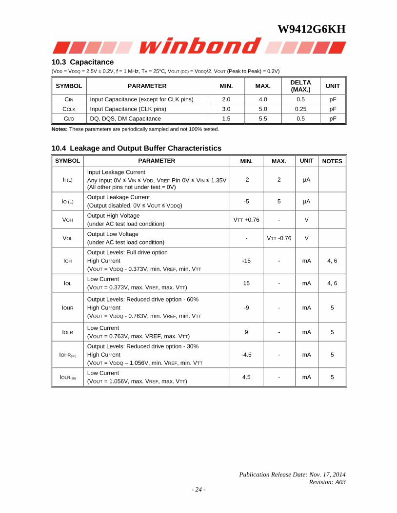
10.3 Capacitance (VDD = VDDQ = 2.5V ± 0.2V, f = 1 MHz, TA = 25°C, VOUT (DC) = VDDQ/2, VOUT (Peak to Peak) = 0.2V)
SYMBOL PARAMETER MIN. MAX. DELTA (MAX.)
UNIT
CIN Input Capacitance (except for CLK pins) 2.0 4.0 0.5 pF
CCLK Input Capacitance (CLK pins) 3.0 5.0 0.25 pF
CI/O DQ, DQS, DM Capacitance 1.5 5.5 0.5 pF
Notes: These parameters are periodically sampled and not 100% tested.
10.4 Leakage and Output Buffer Characteristics
SYMBOL PARAMETER MIN. MAX. UNIT NOTES
II (L)
Input Leakage Current
Any input 0V ≤ VIN ≤ VDD, VREF Pin 0V ≤ VIN ≤ 1.35V (All other pins not under test = 0V)
-2 2 µA
IO (L) Output Leakage Current
(Output disabled, 0V ≤ VOUT ≤ VDDQ) -5 5 µA
VOH Output High Voltage
(under AC test load condition) VTT +0.76 - V
VOL Output Low Voltage
(under AC test load condition) - VTT -0.76 V
IOH
Output Levels: Full drive option
High Current
(VOUT = VDDQ - 0.373V, min. VREF, min. VTT
-15 - mA 4, 6
IOL Low Current
(VOUT = 0.373V, max. VREF, max. VTT) 15 - mA 4, 6
IOHR
Output Levels: Reduced drive option - 60%
High Current
(VOUT = VDDQ - 0.763V, min. VREF, min. VTT
-9 - mA 5
IOLR Low Current
(VOUT = 0.763V, max. VREF, max. VTT) 9 - mA 5
IOHR(30)
Output Levels: Reduced drive option - 30%
High Current
(VOUT = VDDQ – 1.056V, min. VREF, min. VTT
-4.5 - mA 5
IOLR(30) Low Current
(VOUT = 1.056V, max. VREF, max. VTT) 4.5 - mA 5

W9412G6KH
Publication Release Date: Nov. 17, 2014
Revision: A03
- 25 -
10.5 DC Characteristics
SYM. PARAMETER MAX.
UNIT NOTES -5/-5I -6I
IDD0
Operating current: One Bank Active-Precharge;
tRC = tRC min; tCK = tCK min;
DQ, DM and DQS inputs changing once per clock cycle;
Address and control inputs changing once every two clock cycles
55 50 7
IDD1
Operating current: One Bank Active-Read-Precharge;
Burst = 4; tRC = tRC min; CL = 3; tCK = tCK min; IOUT = 0 mA;
Address and control inputs changing once per clock cycle.
65 55 7, 9
IDD2P
Precharge Power Down standby current:
All Banks Idle; Power down mode;
CKE ≤ VIL max; tCK = tCK min; Vin = VREF for DQ, DQS and DM
5 5
IDD2N
Idle standby current:
CS ≥ VIH min; All Banks Idle; CKE ≥ VIH min; tCK = tCK min;
Address and other control inputs changing once per clock cycle;
Vin ≥ VIH min or Vin ≤ VIL max for DQ, DQS and DM
20 20 7
IDD3P
Active Power Down standby current:
One Bank Active; Power down mode;
CKE ≤ VIL max; tCK = tCK min;
Vin = VREF for DQ, DQS and DM
10 10
IDD3N
Active standby current:
CS ≥ VIH min; CKE ≥ VIH min; One Bank Active-Precharge;
tRC = tRAS max; tCK = tCK min;
DQ, DM and DQS inputs changing twice per clock cycle;
Address and other control inputs changing once per clock cycle
30 30 mA 7
IDD4R
Operating current:
Burst = 2; Reads; Continuous burst; One Bank Active;
Address and control inputs changing once per clock cycle;
CL=2; tCK = tCK min; IOUT = 0mA
120 110 7, 9
IDD4W
Operating current:
Burst = 2; Write; Continuous burst; One Bank Active;
Address and control inputs changing once per clock cycle;
CL = 2; tCK = tCK min;
DQ, DM and DQS inputs changing twice per clock cycle
115 100 7
IDD5 Auto Refresh current: tRC = tRFC min 70 65 7
IDD6 Self Refresh current: CKE ≤ 0.2V; external clock on; tCK = tCK min 2 2
IDD7
Random Read current: 4 Banks Active Read with activate every 20nS, Auto-Precharge Read every 20 nS;
Burst = 4; tRCD = 3; IOUT = 0mA;
DQ, DM and DQS inputs changing twice per clock cycle;
Address changing once per clock cycle
150 130

W9412G6KH
Publication Release Date: Nov. 17, 2014
Revision: A03
- 26 -
10.6 AC Characteristics and Operating Condition
SYM. PARAMETER -5/-5I -6I
UNIT NOTES MIN. MAX. MIN. MAX.
tRC Active to Ref/Active Command Period 50 54
nS
tRFC Ref to Ref/Active Command Period 70 70
tRAS Active to Precharge Command Period 40 100000 42 100000
tRCD Active to Read/Write Command Delay Time 15 18
tRAP Active to Read with Auto-precharge Enable 15 18
tCCD Read/Write(a) to Read/Write(b) Command Period 1 1 tCK
tRP Precharge to Active Command Period 15 18
nS
tRRD Active(a) to Active(b) Command Period 10 12
tWR Write Recovery Time 15 15
tDAL Auto-precharge Write Recovery + Precharge Time (tWR/tCK)
+ (tRP/tCK)
(tWR/tCK)
+ (tRP/tCK)
tCK 18
tCK CLK Cycle Time
CL = 2 7.5 12 7.5 12
nS
CL = 2.5 6 12 6 12
CL = 3 5 12 6 12
tAC Data Access Time from CLK, CLK -0.7 0.7 -0.7 0.7 16
tDQSCK DQS Output Access Time from CLK, CLK -0.6 0.6 -0.6 0.6 16
tDQSQ Data Strobe Edge to Output Data Edge Skew 0.4 0.4
tCH CLk High Level Width 0.45 0.55 0.45 0.55 tCK 11
tCL CLK Low Level Width 0.45 0.55 0.45 0.55
tHP CLK Half Period (minimum of actual tCH, tCL) min
(tCL,tCH)
Min,
(tCL,tCH)
nS
tQH DQ Output Data Hold Time from DQS tHP-0.5 tHP-0.5
tRPRE DQS Read Preamble Time 0.9 1.1 0.9 1.1 tCK 11
tRPST DQS Read Postamble Time 0.4 0.6 0.4 0.6
tDS DQ and DM Setup Time to DQS, slew rate 0.5V/nS 0.4 0.4
nS
tDH DQ and DM Hold Time to DQS, slew rate 0.5V/nS 0.4 0.4
tDIPW DQ and DM Input Pulse Width (for each input) 1.75 1.75
tDQSH DQS Input High Pulse Width 0.35 0.35
tCK 11 tDQSL DQS Input Low Pulse Width 0.35 0.35
tDSS DQS Falling Edge to CLK Setup Time 0.2 0.2
tDSH DQS Falling Edge Hold Time from CLK 0.2 0.2
tWPRES Clock to DQS Write Preamble Set-up Time 0 0 nS
tWPRE DQS Write Preamble Time 0.25 0.25
tCK 11 tWPST DQS Write Postamble Time 0.4 0.6 0.4 0.6
tDQSS Write Command to First DQS Latching Transition 0.75 1.25 0.75 1.25
tIS Input Setup Time (fast slew rate) 0.6 0.75
nS
19, 21-23
tIH Input Hold Time (fast slew rate) 0.6 0.75 19, 21-23
tIS Input Setup Time (slow slew rate) 0.7 0.8 20-23
tIH Input Hold Time (slow slew rate) 0.7 0.8 20-23
tIPW Control & Address Input Pulse Width (for each input) 2.2 2.2
tHZ Data-out High-impedance Time from CLK, CLK 0.7 0.7
tLZ Data-out Low-impedance Time from CLK, CLK -0.7 0.7 -0.7 0.7
tT(SS) SSTL Input Transition 0.5 1.5 0.5 1.5
tWTR Internal Write to Read Command Delay 2 1 tCK
tXSNR Exit Self Refresh to non-Read Command 75 75 nS
tXSRD Exit Self Refresh to Read Command 200 200 tCK
tREFI Refresh Interval Time (4K/ 64mS) 15.6 15.6 µS 17
tMRD Mode Register Set Cycle Time 10 12 nS

W9412G6KH
Publication Release Date: Nov. 17, 2014
Revision: A03
- 27 -
10.7 AC Test Conditions
PARAMETER SYMBOL VALUE UNIT
Input High Voltage (AC) VIH VREF + 0.31 V
Input Low Voltage (AC) VIL VREF - 0.31 V
Input Reference Voltage VREF 0.5 x VDDQ V
Termination Voltage VTT 0.5 x VDDQ V
Differential Clock Input Reference Voltage VR Vx (AC) V
Input Difference Voltage. CLK and CLK Inputs (AC) VID (AC) 1.5 V
Output Timing Measurement Reference Voltage VOTR 0.5 x VDDQ V
V SWING (MAX)
VDDQ
VSS
TT
VIH min (AC)
VREF
VIL max (AC)
SLEW = (VIH min (AC) - VILmax (AC)) / T
Output
50 Ω
VTT
Timing Reference Load
Output
V(out)30pF
Notes:
(1) Conditions outside the limits listed under “Absolute Maximum Ratings” may cause permanent damage to the device.
(2) All voltages are referenced to VDD, VDDQ.
(3) Peak to peak AC noise on VREF may not exceed ±2% VREF(DC).
(4) VOH = 1.95V, VOL = 0.35V
(5) VOH = 1.9V, VOL = 0.4V
(6) The values of IOH(DC) is based on VDDQ = 2.3V and VTT = 1.19V. The values of IOL(DC) is based on VDDQ = 2.3V and VTT = 1.11V.
(7) These parameters depend on the cycle rate and these values are measured at a cycle rate with the minimum values of tCK and tRC.
(8) VTT is not applied directly to the device. VTT is a system supply for signal termination resistors is expected to be set equal to VREF and must track variations in the DC level of VREF.
(9) These parameters depend on the output loading. Specified values are obtained with the output open. (10) Transition times are measured between VIH min(AC) and VIL max(AC).Transition (rise and fall) of input signals have a fixed
slope. (11) IF the result of nominal calculation with regard to tCK contains more than one decimal place, the result is rounded up to
the nearest decimal place.
(i.e., tDQSS = 1.25 tCK, tCK = 5 nS, 1.25 5 nS = 6.25 nS is rounded up to 6.2 nS.) (12) VX is the differential clock cross point voltage where input timing measurement is referenced. (13) VID is magnitude of the difference between CLK input level and CLK input level. (14) VISO means {VICK(CLK)+VICK( CLK )}/2. (15) Refer to the figure below.

W9412G6KH
Publication Release Date: Nov. 17, 2014
Revision: A03
- 28 -
CLK
CLK
VSS
VICK
VX VXVX
VXVX
VICK
VICK VICKVID(AC)
VID(AC)
0 V Differential
VISO
VISO(min) VISO(max)
VSS
(16) tAC and tDQSCK depend on the clock jitter. These timing are measured at stable clock.
(17) A maximum of eight AUTO REFRESH commands can be posted to any given DDR SDRAM device.
(18) tDAL = (tWR/tCK) + (tRP/tCK)
For each of the terms above, if not already an integer, round to the next highest integer.
Example: For -5 speed grade at CL=2.5 and tCK=6 nS
tDAL = ((15 nS / 6 nS) + (15 nS / 6 nS)) clocks = ((3) + (3)) clocks = 6 clocks
(19) For command/address input slew rate ≥ 1.0 V/nS.
(20) For command/address input slew rate ≥ 0.5 V/nS and < 1.0 V/nS.
(21) For CLK & CLK slew rate ≥1.0 V/nS (single-ended).
(22) These parameters guarantee device timing, but they are not necessarily tested on each device. They may be guaranteed by device design or tester correlation.
(23) Slew Rate is measured between VOH(ac) and VOL(ac).
W9412G6KH
Publication Release Date: Nov. 17, 2014
Revision: A03
- 29 -
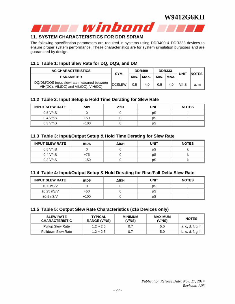
11. SYSTEM CHARACTERISTICS FOR DDR SDRAM
The following specification parameters are required in systems using DDR400 & DDR333 devices to ensure proper system performance. These characteristics are for system simulation purposes and are guaranteed by design.
11.1 Table 1: Input Slew Rate for DQ, DQS, and DM
AC CHARACTERISTICS SYM.
DDR400 DDR333 UNIT NOTES
PARAMETER MIN. MAX. MIN. MAX.
DQ/DM/DQS input slew rate measured between VIH(DC), VIL(DC) and VIL(DC), VIH(DC)
DCSLEW 0.5 4.0 0.5 4.0 V/nS a, m
11.2 Table 2: Input Setup & Hold Time Derating for Slew Rate
INPUT SLEW RATE ΔtIS ΔtIH UNIT NOTES
0.5 V/nS 0 0 pS i
0.4 V/nS +50 0 pS i
0.3 V/nS +100 0 pS i
11.3 Table 3: Input/Output Setup & Hold Time Derating for Slew Rate
INPUT SLEW RATE ΔtDS ΔtDH UNIT NOTES
0.5 V/nS 0 0 pS k
0.4 V/nS +75 0 pS k
0.3 V/nS +150 0 pS k
11.4 Table 4: Input/Output Setup & Hold Derating for Rise/Fall Delta Slew Rate
INPUT SLEW RATE ΔtDS ΔtDH UNIT NOTES
±0.0 nS/V 0 0 pS j
±0.25 nS/V +50 0 pS j
±0.5 nS/V +100 0 pS j
11.5 Table 5: Output Slew Rate Characteristics (x16 Devices only)
SLEW RATE CHARACTERISTIC
TYPICAL RANGE (V/NS)
MINIMUM (V/NS)
MAXIMUM (V/NS)
NOTES
Pullup Slew Rate 1.2 ~ 2.5 0.7 5.0 a, c, d, f, g, h
Pulldown Slew Rate 1.2 ~ 2.5 0.7 5.0 b, c, d, f, g, h

W9412G6KH
Publication Release Date: Nov. 17, 2014
Revision: A03
- 30 -
11.6 Table 6: Output Slew Rate Matching Ratio Characteristics
SLEW RATE CHARACTERISTIC DDR400 DDR333 NOTES
PARAMETER MIN. MAX. MIN. MAX.
Output Slew Rate Matching Ratio (Pullup to Pulldown) 0.67 1.5 0.67 1.5 e, m
11.7 Table 7: AC Overshoot/Undershoot Specification for Address and Control Pins
PARAMETER SPECIFICATION
DDR400 DDR333
Maximum peak amplitude allowed for overshoot 1.5 V 1.5 V
Maximum peak amplitude allowed for undershoot 1.5 V 1.5 V
The area between the overshoot signal and VDD must be less than or equal to Max. area in Figure 3
4.5 V-nS 4.5 V-nS
The area between the undershoot signal and GND must be less than or equal to Max. area in Figure 3
4.5 V-nS 4.5 V-nS
0 0.5 0.68751.0 1.5 2.0 2.5 3.0 3.5 4.0 4.5 5.0 5.5 6.06.3125 6.5 7.0
-5
-4
-3
-2
-1
0
1
2
3
4
5
Max. amplitude = 1.5V
Overshoot
VDD
Max. area
Max. amplitude = 1.5V GND
UndershootTime (nS)
Vo
lts (
V)
Figure 3: Address and Control AC Overshoot and Undershoot Definition

W9412G6KH
Publication Release Date: Nov. 17, 2014
Revision: A03
- 31 -
11.8 Table 8: Overshoot/Undershoot Specification for Data, Strobe, and Mask Pins
PARAMETER SPECIFICATION
DDR400 DDR333
Maximum peak amplitude allowed for overshoot 1.2 V 1.2 V
Maximum peak amplitude allowed for undershoot 1.2 V 1.2 V
The area between the overshoot signal and VDD must be less than or equal to Max. area in Figure 4
2.4 V-nS 2.4 V-nS
The area between the undershoot signal and GND must be less than or equal to Max. area in Figure 4
2.4 V-nS 2.4 V-nS
0 0.5 1.0 1.42 1.5 2.0 2.5 3.0 3.5 4.0 4.5 5.0 5.5 5.68 6.0 6.5 7.0
-5
-4
-3
-2
-1
0
1
2
3
4
5
Max. amplitude = 1.2V
Overshoot
VDD
Max. area
Max. amplitude = 1.2V GND
UndershootTime (nS)
Vo
lts (
V)
Figure 4: DQ/DM/DQS AC Overshoot and Undershoot Definition

W9412G6KH
Publication Release Date: Nov. 17, 2014
Revision: A03
- 32 -
11.9 System Notes:
a. Pullup slew rate is characterized under the test conditions as shown in Figure 1.
VSSQ
50Ω
Output
Test point
Figure 1: Pullup slew rate test load
b. Pulldown slew rate is measured under the test conditions shown in Figure 2.
VDDQ
50Ω
Output
Test point
Figure 2: Pulldown slew rate test load
c. Pullup slew rate is measured between (VDDQ/2 - 320 mV ± 250 mV)
Pulldown slew rate is measured between (VDDQ/2 + 320 mV ± 250 mV)
Pullup and Pulldown slew rate conditions are to be met for any pattern of data, including all outputs switching and only one output switching.
Example: For typical slew rate, DQ0 is switching
For minimum slew rate, all DQ bits are switching worst case pattern
For maximum slew rate, only one DQ is switching from either high to low, or low to high
The remaining DQ bits remain the same as for previous state
d. Evaluation conditions
Typical: 25°C (T Ambient), VDDQ = nominal, typical process
Minimum: 70°C (T Ambient), VDDQ = minimum, slow-slow process
Maximum: 0°C (T Ambient), VDDQ = maximum, fast-fast process

W9412G6KH
Publication Release Date: Nov. 17, 2014
Revision: A03
- 33 -
e. The ratio of pullup slew rate to pulldown slew rate is specified for the same temperature and voltage, over the entire temperature and voltage range. For a given output, it represents the maximum difference between pullup and pulldown drivers due to process variation.
f. Verified under typical conditions for qualification purposes.
g. TSOP II package devices only.
h. Only intended for operation up to 266 Mbps per pin.
i. A derating factor will be used to increase tIS and tIH in the case where the input slew rate is below 0.5 V/nS as shown in Table 2. The Input slew rate is based on the lesser of the slew rates determined by either VIH(AC) to VIL(AC) or VIH(DC) to VIL(DC), similarly for rising transitions.
j. A derating factor will be used to increase tDS and tDH in the case where DQ, DM, and DQS slew rates differ, as shown in Tables 3 & 4. Input slew rate is based on the larger of AC-AC delta rise, fall rate and DC-DC delta rise, fall rate. Input slew rate is based on the lesser of the slew rates determined by either VIH(AC) to VIL(AC) or VIH(DC) to VIL(DC), similarly for rising transitions.
The delta rise/fall rate is calculated as:
{1/(Slew Rate1)}-{1/(slew Rate2)}
For example: If Slew Rate 1 is 0.5 V/nS and Slew Rate 2 is 0.4 V/nS, then the delta rise, fall rate is
-0.5 nS/V. Using the table given, this would result in the need for an increase in tDS and tDH of 100 pS.
k. Table 3 is used to increase tDS and tDH in the case where the I/O slew rate is below 0.5 V/nS. The I/O slew rate is based on the lesser of the AC-AC slew rate and the DC-DC slew rate. The input slew rate is based on the lesser of the slew rates determined by either VIH(AC) to VIL(AC) or VIH(DC) to VIL(DC), and similarly for rising transitions.
m. DQS, DM, and DQ input slew rate is specified to prevent double clocking of data and preserve setup and hold times. Signal transitions through the DC region must be monotonic.

W9412G6KH
Publication Release Date: Nov. 17, 2014
Revision: A03
- 34 -
12. TIMING WAVEFORMS
12.1 Command Input Timing
CLK
CLK
tCK
tCK
tCLtCH
tIS tIH
tIS tIH
tIS tIH
tIS tIH
tIS tIH
CS
RAS
CAS
WE
A0~A11
BA0,1
Refer to the Command Truth Table
12.2 Timing of the CLK Signals
tCK
tT tT
VIH
VIH(AC)
VIL(AC)
VILCLK
CLK
CLK
CLK
VX VX VX
VIH
VIL
tCH tCL

W9412G6KH
Publication Release Date: Nov. 17, 2014
Revision: A03
- 35 -
12.3 Read Timing (Burst Length = 4)
tIS tIH
DA0 DA1 DA2
tCH tCL tCK
ADD
CMD
CLK
CLK
READ
Col
QA0 QA1 QA2 DA3QA3
tRPRE
tDQSCK
tDQSCK tDQSCK
tRPST
PostamblePreamble
Hi-Z
Hi-Z
tDQSQ tDQSQ tDQSQ
tQH
tQH
tAC
tLZ
tHZ
Hi-Z
Hi-Z
DA0 DA1 DA2QA0 QA1 QA2 DA3QA3
tRPRE
tDQSCK
tDQSCK tDQSCK
tRPST
PostamblePreamble
Hi-Z
Hi-Z
tDQSQ tDQSQ tDQSQ
tQH
tQH
tAC
tLZ tHZ
Hi-Z
Hi-Z
CAS Latency = 2
DQS
Output
(Data)
CAS Latency = 3
DQS
Output
(Data)
tIS tIH
Notes: The correspondence of LDQS, UDQS to DQ. (W9412G6KH)
LDQS DQ0~7
UDQS DQ8~15

W9412G6KH
Publication Release Date: Nov. 17, 2014
Revision: A03
- 36 -
12.4 Write Timing (Burst Length = 4)
tIS tIH tDSH tDSS tDSStDSH
tWPRES
tDHtDHtDH
tDS tDS tDS
tDQSS tDSH tDSHtDSS tDSS
Postamble
tWPRE
Preamble
tDQSH tDQSHtDQSL tWPST
DA0 DA1 DA2 DA3
tWPRES
tDS tDS
tDQSS
tDSH tDSHtDSS tDSS
Postamble
tWPRE
Preamble
tDQSH tDQSHtDQSL tWPST
tWPRES
tDH
tDS
tDS
tDQSS
Postamble
tWPRE
Preamble
tDQSH tDQSHtDQSL tWPST
DA0 DA1 DA2 DA3
tDS
tDH tDH
tCH tCL tCK
DQS
Input
(Data)
LDQS
DQ0~7
UDQS
DQ8~15
x4, x8 device
x16 device
ADD
CMD
CLK
CLK
WRIT
Col
DA0 DA1 DA2 DA3
DA0 DA1 DA2 DA3
tDHtDHtDH
tDS
DA0 DA1 DA2 DA3DA0 DA1 DA2 DA3
tIS tIH
Note: x16 has two DQSs (UDQS for upper byte and LDQS for lower byte). Even if one of the 2 bytes is not used, both UDQS and LDQS must be toggled.

W9412G6KH
Publication Release Date: Nov. 17, 2014
Revision: A03
- 37 -
12.5 DM, DATA MASK (W9412G6KH)
WRIT
tDIPW
tDIPW
tDHtDHtDStDS
Masked
CLK
CMD
LDQS
LDM
DQ0~DQ7 D3D1D0
tDIPW
tDIPW
tDHtDHtDStDS
Masked
UDQS
UDM
DQ8~DQ15 D3D2D0
CLK

W9412G6KH
Publication Release Date: Nov. 17, 2014
Revision: A03
- 38 -
12.6 Mode Register Set (MRS) Timing
MRS
Register Set data
NEXT CMD
tMRD
CLK
CLK
CMD
ADD
A2 A1 A0
A3
A6 A5 A4
A8
BA1 BA0
0 0 0
0 0 0
0 0 1
0 1 0
0 1 1
1 0 0
1 0 1
1 1 0
1 1 1
0 0 1
0 1 0
0 1 1
1 0 0
1 0 1
1 1 0
1 1 1
0
1
0
1
1
1
0
0
0
1
0
1
2
4
8
2
4
8
Burst Length
Sequential Interleaved
Reserved Reserved
Reserved
Reserved
Reserved
Reserved
Sequential
Interleaved
Addressing Mode
CAS Latency
2
DLL Reset
No
Yes
MRS or EMRS
Regular MRS cycle
Extended MRS cycle
2.5
A0
A1
A2
A3
A4
A5
A6
A7
A8
A9
A10
A11
BA0
BA1 "0"
"0"
"0"
"0"
"0"
"0"
DLL Reset
Reserved
Addressing Mode
* "Reserved" should stay "0" during MRS cycle.
Reserved
Mode Register Set
or
Extended Mode
Register Set
CAS Latency
Burst Length
Reserved Reserved
3

W9412G6KH
Publication Release Date: Nov. 17, 2014
Revision: A03
- 39 -
12.7 Extend Mode Register Set (EMRS) Timing
EMRS
Register Set data
NEXT CMD
tMRD
CLK
CLK
CMD
ADD
A0
BA1 BA0
0
1
1
1
0
0
0
1
0
1
Enable
Disable
DLL Switch
MRS or EMRS
Regular MRS cycle
Extended MRS cycle
A0
A1
A2
A3
A4
A5
A6
A7
A8
A9
A10
A11
BA0
BA1 "0"
"0"
"0"
"0"
"0"
"0"
* "Reserved" should stay "0" during EMRS cycle.
"0"
"0"
"0"
"0"
"0"
"0"
Buffer Strength
DLL Switch
Reserved
Mode Register Set
or
Extended Mode
Register Set
Reserved
Buffer Strength
A1 Buffer Strength
100% Strength
A6
1
1
0
0
0
1
0
1 60% Strength
30% Strength
Reserved

W9412G6KH
Publication Release Date: Nov. 17, 2014
Revision: A03
- 40 -
12.8 Auto-precharge Timing (Read Cycle, CL = 2)
1) tRCD (READA) tRAS (min) – (BL/2) tCK
AP
Q7Q6Q5Q4Q3Q2Q1Q0
ACT READA ACT
Q0 Q1 Q2 Q3
ACTREADAACT
Q0 Q1
ACTAPREADAACT
tRPtRAS
CMD
DQS
DQ
CMD
DQS
DQ
CMD
DQS
DQ
BL=2
BL=4
BL=8
CLK
CLK
AP
Notes: CL=2 shown; same command operation timing with CL = 2,5 and CL=3
In this case, the internal precharge operation begin after BL/2 cycle from READA command.
AP
Represents the start of internal precharging.
The Read with Auto-precharge command cannot be interrupted by any other command.
W9412G6KH
Publication Release Date: Nov. 17, 2014
Revision: A03
- 41 -
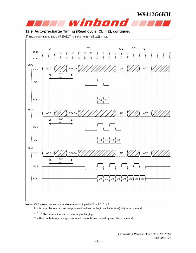
12.9 Auto-precharge Timing (Read cycle, CL = 2), continued
2) tRCD/RAP(min) tRCD (READA) tRAS (min) – (BL/2) tCK
AP
Q7Q6Q5Q4Q3Q2Q1Q0
ACT READA ACT
Q0 Q1 Q2 Q3
ACTREADAACT
Q0 Q1
ACTAPREADAACT
tRPtRAS
CMD
DQS
DQ
CMD
DQS
DQ
CMD
DQS
DQ
BL=2
BL=4
BL=8
CLK
CLK
AP
tRAP
tRCD
tRAP
tRCD
tRAP
tRCD
Notes: CL2 shown; same command operation timing with CL = 2.5, CL=3.
In this case, the internal precharge operation does not begin until after tRAS(min) has command.
AP
Represents the start of internal precharging.
The Read with Auto-precharge command cannot be interrupted by any other command.

W9412G6KH
Publication Release Date: Nov. 17, 2014
Revision: A03
- 42 -
12.10 Auto-precharge Timing (Write Cycle)
AP
ACT
ACTWRITA
ACTWRITACMD
DQS
DQ
CMD
DQS
DQ
CMD
DQS
DQ
BL=2
BL=4
BL=8
CLK
CLK
AP
AP
D0 D1
D0 D1 D2 D3
D0 D1 D2 D3 D4 D5 D6 D7
tDAL
tDAL
tDAL
WRITA
The Write with Auto-precharge command cannot be interrupted by any other command.
AP Represents the start of internal precharging.

W9412G6KH
Publication Release Date: Nov. 17, 2014
Revision: A03
- 43 -
12.11 Read Interrupted by Read (CL = 2, BL = 2, 4, 8)
CMD
ADD
DQS
CLK
CLK
DQ
ACT READ A READ B READ C READ D READ E
Row Address COl,Add,A Col,Add,B Col,Add,C Col,Add,D Col,Add,E
QC0QA0 QA1 QB0 QB1
tCCDtCCDtCCDtCCDtRCD
12.12 Burst Read Stop (BL = 8)
READCMD
DQS
DQ
CLK
CLK
BST
Q0 Q1 Q2 Q3 Q4 Q5
Q0 Q1 Q2 Q3 Q4 Q5
CAS Latency
CAS Latency
CAS Latency = 2
DQS
DQ
CAS Latency = 3

W9412G6KH
Publication Release Date: Nov. 17, 2014
Revision: A03
- 44 -
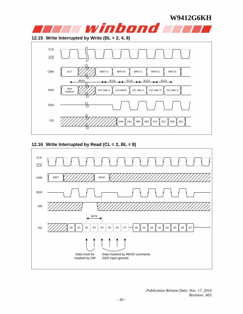
12.13 Read Interrupted by Write & BST (BL = 8)
READCMD
DQS
DQ
CLK
CLK
BST
Q0 Q1 Q2 Q3 Q4 Q5
CAS Latency = 2
WRIT
D0 D1 D2 D3 D4 D5 D6 D7
Burst Read cycle must be terminated by BST Command to avoid I/O conflict.
12.14 Read Interrupted by Precharge (BL = 8)
READCMD
DQS
DQ
CLK
CLK
PRE
Q0 Q1 Q2 Q3 Q4 Q5
Q0 Q1 Q2 Q3 Q4 Q5
CAS Latency
CAS Latency
CAS Latency = 2
DQS
DQ
CAS Latency = 3
W9412G6KH
Publication Release Date: Nov. 17, 2014
Revision: A03
- 45 -
12.15 Write Interrupted by Write (BL = 2, 4, 8)
CMD
ADD
DQS
CLK
CLK
DQ
ACT WRIT A WRIT B WRIT C WRIT D WRIT E
Row
AddressCOl. Add. A Col.Add.B Col. Add. C Col. Add. D Col. Add. E
DC0 DC1 DD0 DD1DA0 DA1 DB0 DB1
tCCDtCCDtCCDtCCDtRCD
12.16 Write Interrupted by Read (CL = 2, BL = 8)
WRITCMD
DQS
DM
CLK
CLK
tWTR
DQ D4 D5 D6 D7D0 D1 D2 D3
Data must be
masked by DM
READ
Data masked by READ command,
DQS input ignored.
Q4 Q5 Q6 Q7Q0 Q1 Q2 Q3
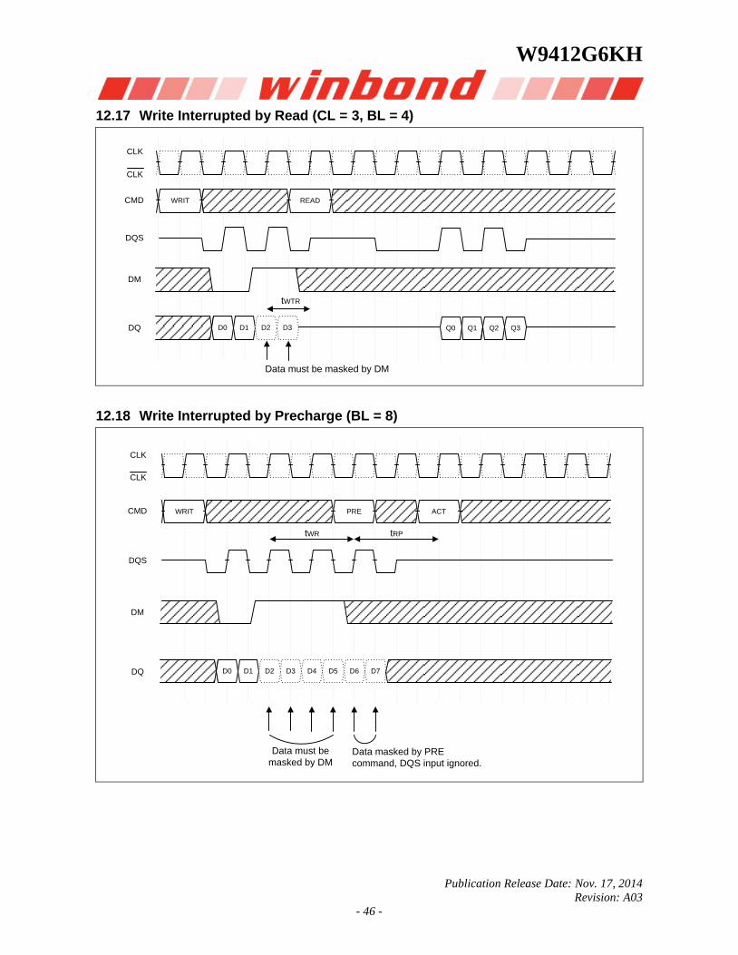
W9412G6KH
Publication Release Date: Nov. 17, 2014
Revision: A03
- 46 -
12.17 Write Interrupted by Read (CL = 3, BL = 4)
WRITCMD
DQS
DM
CLK
CLK
READ
tWTR
DQ Q0 Q1 Q2 Q3D0 D1 D2 D3
Data must be masked by DM
12.18 Write Interrupted by Precharge (BL = 8)
WRITCMD
DQS
DM
CLK
CLK
ACT
tWR
DQ D4 D5 D6 D7D0 D1 D2 D3
Data must be
masked by DM
PRE
tRP
Data masked by PRE
command, DQS input ignored.

W9412G6KH
Publication Release Date: Nov. 17, 2014
Revision: A03
- 47 -
12.19 2 Bank Interleave Read Operation (CL = 2, BL = 2)
CMD
DQS
CLK
CLK
DQ Q0a Q1a Q0b Q1b
ACTa/b : Bank Act. CMD of bank a/b
READAa/b : Read with Auto Pre.CMD of bank a/b
APa/b : Auto Pre. of bank a/b
ACTa ACTb READAa ACTaREADAb ACTb
APa APb
tRCD(a)
tRAS(a) tRP(a)
tRAS(b)
tRCD(b)
tRP(b)
CL(a) CL(b)
Preamble Postamble Preamble Postamble
tRRD
tRC(a)
tRC(b)
tRRD
12.20 2 Bank Interleave Read Operation (CL = 2, BL = 4)
CMD
DQS
CLK
CLK
DQ Q2a Q3a Q2b Q3b
ACTa/b : Bank Act. CMD of bank a/b
READAa/b : Read with Auto Pre.CMD of bank a/b
APa/b : Auto Pre. of bank a/b
ACTa READAaACTb READAb ACTa ACTb
APa APb
tRCD(a)
tRAS(a) tRP(a)
tRAS(b)
tRCD(b)
tRP(b)
CL(a) CL(b)
Preamble Postamble
tRRD
tRC(a)
tRC(b)
tRRD
Q0a Q1a Q0b Q1b

W9412G6KH
Publication Release Date: Nov. 17, 2014
Revision: A03
- 48 -
12.21 4 Bank Interleave Read Operation (CL = 2, BL = 2)
CMD
DQS
CLK
CLK
DQ Q0a Q1a Q0b Q1b
ACTa/b/c/d : Bank Act. CMD of bank a/b/c/d
READAa/b/c/d : Read with Auto Pre.CMD of bank a/b/c/d
APa/b/c/d : Auto Pre. of bank a/b/c/d
ACTa ACTb READAaACTc READAbACTd READAcACTa
APa APb
tRCD(a)
tRAS(a) tRP
tRAS(b)
tRCD(b)
CL(a) CL(b)
Preamble Postamble Preamble
tRRD
tRC(a)
tRRD
tRAS(c)
tRAS(d)
tRCD(d)
tRCD(c)
tRRD tRRD
12.22 4 Bank Interleave Read Operation (CL = 2, BL = 4)
CMD
DQS
CLK
CLK
DQ
ACTa/b/c/d : Bank Act. CMD of bank a/b/c/d
READAa/b/c/d : Read with Auto Pre.CMD of bank a/b/c/d
APa/b/c/d : Auto Pre. of bank a/b/c/d
ACTa READAaACTb READAbACTc READAcACTd READAdACTa
APa APb
tRCD(a)
tRAS(a) tRP(a)
tRAS(b)
tRCD(b)
CL(a) CL(b)
tRRD
tRC(a)
tRRD
tRAS(c)
tRAS(d)
tRCD(d)
tRCD(c)
tRRD tRRD
Q0b Q1b Q0c Q1c
Preamble
Q2a Q3a Q2b Q3bQ0a Q1a
CL(c)
APc

W9412G6KH
Publication Release Date: Nov. 17, 2014
Revision: A03
- 49 -
12.23 Auto Refresh Cycle
CMD
CLK
CLK
PREA AREF AREF CMDNOP NOP NOP
tRP tRFC tRFC
Note: CKE has to be kept “High” level for Auto-Refresh cycle.
12.24 Precharge/Activate Power Down Mode Entry and Exit Timing
CMD
CLK
CLK
NOP CMDNOP
ExitEntry
CMD NOP
tIH tIS tCK tIH tIS
CKE
Precharge/Activate
Note 1,2
Note:
1. If power down occurs when all banks are idle, this mode is referred to as precharge power down.
2. If power down occurs when there is a row active in any bank, this mode is referred to as active power down.
12.25 Input Clock Frequency Change during Precharge Power Down Mode Timing
NOP NOP NOPDLL
RESETNOP NOP CMD
200 clocks
tISFrequency Change
Occurs here
Minmum 2 clocks
required before
changing frequency
Stable new clock
before power down exit
CLK
CLK
CMD
CKE
tRP

W9412G6KH
Publication Release Date: Nov. 17, 2014
Revision: A03
- 50 -
12.26 Self Refresh Entry and Exit Timing
CMD
CLK
CLK
tIH tIS tIH tIS
SELF CMDSELEX NOPNOPPREA
ExitEntry
CKE
tRP
tXSRD
NOPSELF
tXSNR
SELFX NOP ACT READ NOP
ExitEntry
Note:
If the clock frequency is changed during self refresh mode, a DLL reset is required upon exit.

W9412G6KH
Publication Release Date: Nov. 17, 2014
Revision: A03
- 51 -
13. PACKAGE SPECIFICATION
Package Outline TSOP (TYPE II) 66L 400 mil
Controlling Dimension : Millimeters
E1
e b
1 33
66 34
E
SEATING PLANE
D
A2
A1
A
ZD
Y
DETAIL “A”
L
RAD. R
L1
θθ1
c
RAD. R1
DETAIL “A”
SYMBOLDIMENSION (mm)
MIN. NOM. MAX.
A
A1
A2
b
c
E
E1
D
L
11.56
10.03
0.65 BASIC
22.09 22.22 22.35
0.12
1.20
0.15
1.05
0.38---0.22
0.95
0.05 ---
1.00
------
0.40
e
DIMENSION (inch)
MIN. NOM. MAX.
0.455
0.395
0.026 BASIC
0.870 0.875 0.880
0.005
0.047
0.006
0.041
0.015---0.009
0.037
0.002 ---
0.039
------
0.016
11.76 11.96
10.16 10.29
0.008---
0.463 0.471
0.400 0.405
0.50 0.60 0.020 0.024
0.80 BASIC 0.031 BASICL1
R
R1
0.25
---0.12 ---
---0.12 0.010
---0.005 ---
---0.005
0.71 REF 0.028 REFZD
θθ1
Y
8°
20°
0.10---
10° ---
---
---0° 8°
20°
0.004---
10° ---
---
---0°
0.21---
W9412G6KH
Publication Release Date: Nov. 17, 2014
Revision: A03
- 52 -
14. REVISION HISTORY
VERSION DATE PAGE DESCRIPTION
A01 Feb. 07, 2014 All Initial formally datasheet
A02 Apr. 09, 2014 4~5, 23, 25~27 Removed -5K speed grade
A03 Nov. 17, 2014 4, 5, 16, 23, 25, 26,
29~31, 38 Removed -4 speed grade
Important Notice
Winbond products are not designed, intended, authorized or warranted for use as components in systems or equipment intended for surgical implantation, atomic energy control instruments, airplane or spaceship instruments, transportation instruments, traffic signal instruments, combustion control instruments, or for other applications intended to support or sustain life. Further more, Winbond products are not intended for applications wherein failure of Winbond products could result or lead to a situation wherein personal injury, death or severe property or environmental damage could occur.
Winbond customers using or selling these products for use in such applications do so at their own risk and agree to fully indemnify Winbond for any damages resulting from such improper use or sales.