Embed Size (px)
Citation preview

Washington University in St. Louis
School of Engineering and Applied Science
Electrical and Systems Engineering Department
ESE 498
Hypnolarm
By
Xiaoyang Ye, Daniel He, Pei Heng Zheng
Supervisor
Dr. Robert Morley
Submitted in Partial Fulfillment of the Requirement for the BSEE Degree,
Electrical and Systems Engineering Department, School of Engineering and Applied
Science,
Washington University in St. Louis
May 2014

1
Table of Contents
Table of Figures ............................................................................................................................................. 2
Student Statement ........................................................................................................................................ 3
Abstract ......................................................................................................................................................... 3
Acknowledgements ....................................................................................................................................... 3
Problem Formulation .................................................................................................................................... 4
Problem Statement ................................................................................................................................... 4
Ideal Project Specifications ........................................................................................................................... 4
Concept Synthesis ......................................................................................................................................... 9
Concept Generation .................................................................................................................................. 9
EEG Electrode Setup ............................................................................................................................. 9
Analog Filtering and Amplification of EEG signals .............................................................................. 10
Noise Analysis ............................................................................................................................................. 12
Multiplexing and Digital Filtering of sampled EEG Signals .................................................................. 13
Sleep Stage Detection Algorithm ................................................................................................................ 22
Bluetooth Wireless Transmission Module .................................................................................................. 27
Bill of Materials ........................................................................................................................................... 30
Cost Analysis ............................................................................................................................................... 31
Conclusion ................................................................................................................................................... 32
References .................................................................................................................................................. 33
Appendix ..................................................................................................................................................... 34

2
Table of Figures
Figure 1: Optimize Sleep uses sleep tracking data to adjust the user's last sleep cycle to end at the set
alarm time ..................................................................................................................................................... 7
Figure 2: Maximize Productivity uses sleep tracking data to wake the user at the end of the last sleep
cycle .............................................................................................................................................................. 8
Figure 3: Sensor Sheet with EEG sensor array .............................................................................................. 9
Figure 4: EEG sensor with leads and casing ................................................................................................ 10
Figure 5: 2nd order filter implemented with Sallen Key topology ............................................................. 11
Figure 6: Frequency response of 2nd order low pass filter ........................................................................ 12
Figure 7: Multiplexer Function Operations Flowchart ................................................................................ 16
Figure 8: Convolution Operations ............................................................................................................... 19
Figure 9: Digital Filter State Chart ............................................................................................................... 20
Figure 10: FIFO Circular Buffer .................................................................................................................... 21
Figure 11: Sleep Stage Characterization by EEG Brain Wave Signals .......................................................... 22
Figure 12: 3-D Plot of EEG Samples forming Sleep Stage Clusters ............................................................. 24
Figure 13: Sleep Detection Algorithm Flowchart ........................................................................................ 24
Figure 14 ..................................................................................................................................................... 27
Figure 15 ..................................................................................................................................................... 28
Figure 16 ..................................................................................................................................................... 29
Figure 17: 2nd order low pass filter ............................................................................................................. 34
Figure 18: Summing circuit ......................................................................................................................... 34
Figure 19: Low pass filter frequency response data points ........................................................................ 35
Figure 20: Complete circuit frequency response ........................................................................................ 36
Figure 21: Complete circuit frequency response data points ..................................................................... 36

3
Student Statement
The authors have applied ethics during the design process and complied with the WUSTL Honor Code.
Abstract
Sleep is a necessary part of human life. In today’s world, the amount of time we spend sleeping can be
regularly lower than the National Institutes of Health recommendation of 7 – 8 hours. Studies have
shown that waking up during Rapid Eye Movement (REM) or Stage 1 sleep results in low sleep inertia.
Sleep inertia is a state of lowered arousal that occurs upon waking from sleep and results in temporarily
reduced performance. Similarly, studies show that waking during slow wave sleep (SWS) causes the
most sleep inertia out of all the sleep stages. In addition, sleep inertia becomes worse with sleep
deprivation.
The goal of our project is to create a device that improves lifestyle and productivity by targeting the
sleep stage at waking as something that can be optimized. HypnoLarm is a pillow device that records
and analyzes electroencephalogram (EEG) signals that characterize sleep stage. Using this information
and user-input waking time range, HypnoLarm will be able to wake the user at the optimal time to
minimize sleep inertia while maximizing sleep time. This semester we have been able to build analog
circuitry to collect/filter 8 channels of EEG signal as well as develop algorithms to interpret the data.
Acknowledgements
The authors would like to thank Dr. Robert Morley for his guidance and expertise in design. Without his
help we would not have made as much progress as we did.

4
Problem Formulation
Problem Statement
Sleep inertia is the phenomena of disorientation and reduced performance that occurs immediately
after waking. The time duration of sleep inertia can last from one minute to four hours [1]. Literature
has shown that waking during stage 1 or stage 2 sleep reduces the effects of sleep inertia. In this
project, we aim to design a device that will optimize the waking stage of the user and his/her desired
waking time. By use of electroencephalography (EEG), we aim to be more accurate in determining user
sleep stage than current commercial products that enhance user sleep. The ultimate goal of our device
is to reduce user sleep inertia in order to increase productivity.
Ideal Project Specifications
Sensor Sheet
The sensor sheet is composed of a layered sheet with a memory foam base for comfort. This sheet is
embedded with EEG electrodes and localization sensors. The electrodes are spaced 1 inch apart, center-
to-center in order to best replicate clinical EEG setting. The localization sensors are placed in a layout
such that their data output can be used to determine the orientation and position of the user’s rested
head. The layered sheet is composed of materials of different density in order to maximize both comfort
of the sheet and electrode contact with the user.
Central Processing Circuit
The central processing circuit is composed of a processing board and auxiliary circuit components that
allow piping of data produced by the sensor sheet to and from the processing board. Prior to sending
sensor sheet data to the Mobile App, the central processing circuit must multiplex, amplify and filter the
sensor sheet data to get both meaningful EEG and localization signals. These signals are then stored in
memory as a data time series until sufficient data to produce a sample is generated. The sample is then
transferred over Bluetooth to the Mobile App for sleep analytics processing. After transfer, a percentage
of the buffer is flushed in order to ensure some amount of time overlap between samples.

5
The central processing circuit Bluetooth capability also includes handling incoming control signals from
the Mobile App. These control signals include, but are not limited to, sensor calibration commands and
alarm trigger commands.
Sleeve Alarm
The sleeve alarm is capable at vibrating at various frequencies and strengths in order to suit the needs of
user-defined waking methods. In order to induce micro-awakenings, the sleeve alarm has a high
frequency, low amplitude vibration mode. In order to ease the user awake, the sleeve alarm has a
variable low frequency, increasing amplitude vibration mode. These modes are controlled by the alarm
trigger commands that are sent from the Mobile App through Bluetooth communication.
Functions of the Mobile App
Platforms and Administrative requirements
The Mobile App can be used on both Java-based Android platform and C-based Windows and iOS
platforms. Code has high cross portability through the use of multi-platform integrated extended Python
languages (Jython and Cython). To process data during sleep, the Mobile App must be provided
permissions to access clock, alarm and storage capabilities of the respective development platforms
Sample/Channel Selection and Storage
Using the localization signal and the intrinsic quality of the EEG signal samples, the Mobile App selects
which EEG samples are ideal for sleep stage prediction. The quality is determined by sample
characteristics such as signal-to-noise ratio and the position of the user’s head determined by the
localization signal. Regardless of the selected channel, all channels have their data stored for post-night
processing and analytics, and are labeled with their appropriate physical positions (on the user’s head)
using the localization signal.

6
Sleep Stage Classifier
A sleep stage classifier is implemented to deduce the sleep stage of given sample. The sleep stage
classifier uses a supervised machine learning method in order to classify samples based on initial
datasets. Due to the free-form nature of the sensor sheet, the initial training data for the machine
learning method must be created from data extracted and manually scored from the sensor sheet.
Alarm Control Loop
The alarm control loop takes the predicted sleep stage and time stamp for a sample and stores it in
memory. Using the history of sleep stages and user input wake time, the alarm control loop evaluates
the current state of the alarm and communicates as an alarm trigger command to the Sleeve via
Bluetooth.
Alarm Modes
The user can specify two different alarm modes to produce different degrees of sleep control and
waking. In the “Optimize Sleep” alarm mode, the user is subjected to micro-awakenings through
vibrations from the Sleeve Alarm. These micro-awakenings serve the purpose of regulating the sleep
cycle such that the optimized waking time coincides with the user input wake time.

7
Figure 1: Optimize Sleep uses sleep tracking data to adjust the user's last sleep cycle to end at the set alarm time
In the “maximize productivity” alarm mode, the alarm patterns the sleep cycles of the user and uses the
pattern to find an optimal waking time within a half of a sleep cycle duration of the user’s input wake
time. The sleeve alarm is then triggered to wake the use at the prescribed time. Due to the volatility of
sleep cycles, these modes require the alarm control loop to dynamically solve the optimal wake time
throughout the night.

8
Figure 2: Maximize Productivity uses sleep tracking data to wake the user at the end of the last sleep cycle
User interface
The Mobile App has a graphic user interface (GUI) that allows the user to specify wake times and alarm
modes. The GUI can also access sleep analytics for stored sleep data that are presented as tables and
plots. The code is loosely constructed to allow flexibility in adding additional graphics and modules.

9
Concept Synthesis
The HypnoLarm project is the brainchild of Forty Winks, LLC. Its inception was observed in the BME
senior design class of fall 2012, where one of the company’s founding members saw the potential in
creating a reliable yet unobtrusive sleep optimization device. As a student in the engineering
department, Piero Mendez realized how valuable sleep really is and just how much impact a product
which scientifically improves our quality of sleep can have on society. Thus, the goal for developing a
reliable and comfortable sleep optimization system was created. Since its beginning, HypnoLarm has
encountered numerous setbacks and difficulties such as performing freeform EEG measuring.
Complicated approaches such as using an integrated EEG/Pressure sensor array were proposed, tested
and discarded. In order to push the dream of HypnoLarm into becoming reality, the team has decided to
tackle the fundamentals of the task: by starting with designing the analog circuitry for a single EEG
sensor and moving on from there.
Concept Generation
EEG Electrode Setup
The sensor sheet is composed of polyurethane foam, a material similar in conductive and physical
properties to memory foam, with embedded EEG electrodes. The electrodes are arranged in an array
such that they are 3 inches apart center-to-center. Our current prototype has seven recording
electrodes and one ground electrode as shown in Figure 3 below.
Figure 3: Sensor Sheet with EEG sensor array

10
The polyurethane foam provides a comfortable surface for the user to lie on and has insulative
properties to ensure the electrodes are only recording voltage data from the user’s scalp.
Figure 4 below depicts the EEG electrode setup used in this project, including the shielding wire and
casing.
Figure 4: EEG sensor with leads and casing
The electrode used is an Ag-AgCl EL120 electrode. An audio cable containing internal static shielding was
used to construct the electrode leads; acting like a Faraday’s cage and preventing effects from external
voltage sources. The electrodes are housed within an insulative ABS plastic 3D printed electrode case,
which facilitates contact between the electrodes and the audio wire.
The audio wire is first stripped on its end to expose the wire, which is then wrapped around the end of
the electrode and held in place using the 3D printed case. The case is secured onto the electrode using
super glue. The end of each sensor’s lead is then connected via soldering to an analog circuit which
performs filtering and amplification of EEG signals.
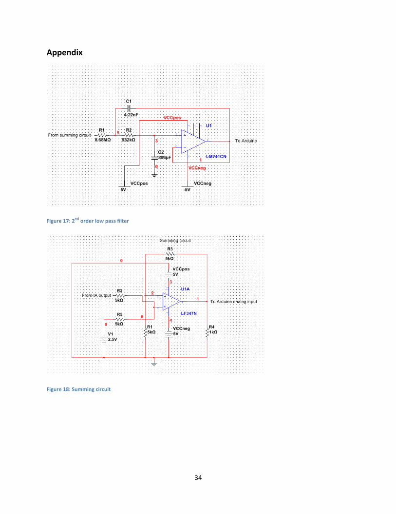
Analog Filtering and Amplification of EEG signals
Our initial analog design was based on a do-it-yourself, EEG circuit [1]. It consisted of an
instrumentation amplifier (IA), two 60 Hz notch filters, 7 Hz high pass filter, 31 Hz low pass filter and 1 Hz

11
high pass gain filter before reaching the A/D converter. Because this design is made to record awake
EEG signals (which have higher frequency content than sleep EEG), it is not completely suitable for our
needs. Our frequency range of interest is in the 1 – 30 Hz range. This range will allow us to capture data
for all of the sleep stages and some waking frequencies.
We decided to drop the two 60 Hz notch filters since the 30 Hz low pass filter would attenuate some of
the noise that occurs at 60 Hz. In addition, the remainder of the power at 60 Hz can be filtered out
digitally and saves us from needing to use two operational amplifiers.
Since our frequency range of interest extends down to 1 Hz, we only utilize a 30 Hz low pass filter
instead of high pass and low pass filter. Again, we can implement the 1 Hz high pass filter digitally while
saving us the cost of a component. The low pass filter is second order filter designed using the Sallen
Key topology (figure 5).
Figure 5: 2nd order filter implemented with Sallen Key topology
Using formulas found in [3], we derive R1 = 8.192MΩ, R2 = 1.005MΩ, C1 = 4.22 nF and C2 = 806 pF.
Appendix A shows our filter circuit implemented with a LM741CN operational amplifier. Figure 6 shows
that we get unity gain below 30 Hz and our 3dB point is very close to 30 Hz.

12
Figure 6: Frequency response of 2nd order low pass filter
Our instrumentation amplifier is an AD620AN and set to have a linear gain of 91 (39dB). For our initial
prototype, we did not use analog multiplexers because the time constant introduced by the second
order filter causes problems when we sample each channel in the multiplexer. Instead, since the
Arduino has 8 analog inputs, we have 8 sets of the analog circuit collecting data and inputting into the
Arduino.
The next problem we encountered was the operating voltage range of the Arduino. The Arduino
operates from 0 – 5V while our EEG signal is centered around 0 and can take on negative values. To fix
this, we implement a summing circuit that will shift the EEG signal up 2.5V so that it is in the operating
range of the Arduino (Appendix).
Noise Analysis
We need to consider the noise coming from the circuit and from quantization of the signal at the A/D
converter of the Arduino. The Arduino is a 10 bit A/D. With an operating voltage of 5V, we get a step
size of
.
Noise VRMS = 1.41 mV.
-50
-40
-30
-20
-10
0
1 10 100 1000
Gain (dB)
Frequency (Hz)
LPF Frequency Response
Series1

13
Noise power = 1.986 uW in fs / 2 = 625 Hz.
The amount of power located in our range of interest is
Noise VRMS in our range of interest = 308.8 uV
Our IA has an input voltage noise of
√
Noise voltage introduced by IA:
√ √
Noise power introduced by IA:
(Assuming other stages introduce negligible noise contributions when compared to that of the IA)
Total noise power:
Total noise VRMS:
EEG signal amplitude can be expected to be in the microvolt range (~100 uV).
Signal voltage:
Signal-to-noise ratio: (
)
Multiplexing and Digital Filtering of sampled EEG Signals
Multiplexer Function
We chose to use the Arduino Pro mini in our prototype mostly for convenience and ease of use. Instead
of designing a processing component from scratch, using the Arduino allowed us to focus on the other
circuit section designs. When we move away from using pre-constructed microprocessors we will need
to take the following requirements into account:

14
1. Number of analog ports
The Arduino mini has 8 analog inputs which was enough to build a working prototype. When we
expand the sensor array, a system of multiplexers will most likely need to be integrated into the
circuit due to the increased number of electrodes being read. A microprocessor with 4-6 analog
inputs should suffice.
2. Analog to digital converter resolution
Since we are working with biological signals we require a high resolution in order to accurately
analyze the measured EEG. The Arduino has an internal ADC resolution of 10 bits, which is
lower than we would like. Increasing the resolution into the range of 12-16 bits would be ideal,
but we realize that this will affect the processing requirements. At the moment, we based the
gain of the instrumentation amplifier on the resolution of the Arduino ADC, which is about 5
mV.
3. Operating voltage
The Arduino operates at 5 V, and can read values in the range of 0-5 V (0 – 1023). This is an
issue we have had to work around by introducing a 2.5 V shift in the input signals. Ideally, the
new processor would be able to read negative voltages in order to remove the need for the
summing amplifier circuit.
4. Clock speed
Up to this point, we have been working around the processing speed restrictions of the Arduino
when writing the code for it. Increasing ADC resolution and the number of sensors would most
likely be too much for the 16 MHz processor of the Arduino to handle.
The microprocessor’s in-built 8-channel, 10-bit analog-to-digital converter (ADC) operates using a 125
KHz clock signal, which is generated using the Arduino’s 16 MHz system clock at a pre-scaler of 128:
ADC clock frequency = (
)

15
The 8 EEG sensors are connected to the analog input pins on the Arduino board. A simple multiplex-and-
sample function for reading the 8 EEG sensors (channels) was designed and written in C++ language for
the Arduino platform, and subsequently uploaded to the Arduino microprocessor. The multiplex
function code can be found in section A of the Appendix.
The ADC on the Arduino pro mini V5 microprocessor takes a minimum of 13 clock cycles (using a 125
KHz clock) to perform one sample and convert. Thus, a minimum of 104 is needed to read a single
EEG sample. A significant constraint of the 10-bit ADC is its inaccuracy when rapidly switching between
reading different analog inputs due to the Arduino’s sample-and-hold circuit’s tendency to retain a
previously read value. This is even more significant when the analog inputs of the ADC are connected to
sources with high impedance (such as the EEG sensors), which take a significant time to
charge/discharge the sample-and-hold circuit’s capacitor. In order to prevent this, the ADC must be
called twice to read another analog input channel:
1. An initial call triggers the ADC to select the new channel to be read.
2. A time delay then allows it to stabilize.
3. The next call to read the same channel will allow the ADC to perform an accurate conversion
and return the correct value.
The multiplex-and-sample function was designed taking the sensing requirements and ADC
considerations mentioned above. The result is a state machine implementation, which consecutively
cycles through reading each of the 8 EEG inputs to the ADC once every 10 milliseconds, and with delays
between switch-and-reads. The code utilizes various Arduino in-built functions such as analogRead(pin),
and delayMicroseconds(time) in order to perform its functions. Figure 7 below depicts the state
diagram of the function.

16
The multiplexer function utilizes the Arduino timer function to sample all 8 EEG channels once every 5
milliseconds, maintaining a constant sample rate of 100Hz for every channel. During one sampling
operation, the code iterates through the 8 channels; first selecting the channel, then delaying 150 to
allow the ADC to stabilize around the channel’s voltage before reading it, followed by another
delay. This gives a total time of per channel and 4 milliseconds for reading all 8 channels, which
falls within the time constraint of 10 milliseconds for a 100 Hz sampling rate per channel.
After each sampling operation, the converted digital values of the 8 EEG channels are sent out via serial
communication, as an 8-index array, where they undergo digital filtering.
The multiplexer code was tested for its ability to maintain a constant 100Hz sampling frequency for
every channel. The Arduino “millis()” function was used to repeatedly read the time between successive
sampling of one channel in milliseconds, which was then printed out. A precise time of 10ms was
maintained throughout.
We then tested its accuracy by feeding 8 known voltage values to the Arduino’s analog input pins using
the NI-Elvis prototyping board, and the ADC’s converted values were printed out and compared to the
actual analog values. Table 1 below shows the results of this accuracy test:
Figure 7: Multiplexer Function Operations Flowchart

17
Table 1: Multiplexer Test Results
Analog Input Pin\Voltage Input ADC Digital Value
A0\2.5V 512
A1\0V 0
A2\5V 1023
A3\0V 0
A4\2.5V 511
A5\5V 1022
A6\0V 1
A7\5V 1023
Thus, we see that the multiplexer code is able to accurately sample every input channel of the ADC while
rapidly iterating through reading each channel at 100Hz. However when we tried to up the sample rate
to 200Hz, the accuracy of the ADC fell visibly. We found that this is because the sample-and-convert
operation of the ADC does not always precisely take 104 , and in order to sample 8 channels at 200Hz
each, the 150 delay has to be decreased to maintain a constant sample frequency. This leads to the
ADC not having enough time to stabilize before reading a channel.

18
Digital FIR Filter
Given that the EEG signals collected by the sensor sheet have a spectrum of interest in the .5 Hz to 30 Hz
interval, a digital low-pass filter with a frequency cutoff at 30Hz was implemented in C++ code on the
Arduino. The digital filter was implemented using the convolution method, which is summarized and
explained below.
The convolution of two functions f and g (f*g) is defined as:
Given a fixed sample rate, the index of each EEG data point can be represented as a step in the time
domain. In other words, the convolution result, y[n] can be expressed as:
Where n is the total number of samples passed in. Since the impulse response is finite, it only has a fixed
number of data points which are not equal to 0. Given i number of non-zero data points in the impulse
response, there are only i terms in the convolution result. Furthermore, h[k] for k<0 and k>i would be 0,
thus the convolution equation’s boundaries change to: from k = n – i to k = n.
Expanding the convolution equation:
y[n] = x[n – i]*h[i] + x[n – i – 1]*h[i – 1] + ….+x[n]*h[0]
Thus, convolution flips the order of the EEG dataset, and performs a multiply-and-addition with the
impulse response terms. It is a First-in-First-Out (FIFO) operation, which does i multiplies and

19
accumulates on the i most recent EEG signal inputs, where i is the number of impulse response terms.
Its operations flowchart is depicted in Figure 8 below.
Figure 8: Convolution Operations
The impulse response of the filter was generated using design tool at:
http://www.arc.id.au/FilterDesign.html. A cutoff frequency of 30 Hz was set for a low-pass filter with a
sample rate of 200Hz, and a length of 59 impulse terms was chosen to minimize the delay introduced by
the filter.
x[n] * h[0]
y[n]
x[n - 1] * h[1]
.…
x[n - i] * h[i]

20
Figure 9 below depicts the state diagram of the digital filter.
Figure 9: Digital Filter State Chart
The digital filter was implemented in C++ as a state machine. It utilizes a FIFO circular buffer of size 59 to
store incoming EEG data, and perform dot product with impulse response coefficients. An “end” pointer
declares the index in the array where new EEG data will be stored, incrementing by one after the data is
written in.

21
Figure 10 illustrates how the circular buffer operates.
Figure 10: FIFO Circular Buffer
Each time new EEG data is read, the end pointer shifts to the next index. This process repeats until the
end pointer reaches the largest index of the buffer array, at which point it resets to zero, and new data
will replace data at index 0.
The digital filter first initializes all values stored in the circular buffer to 0, resetting itself. It then loads
the impulse response coefficients as a header file for use during convolution calculations. Next, EEG data
points are passed in sequentially one at a time and convolution is performed after each data is passed
in. The results of the convolution operation give the time response of the signal to the filter.
end
0
1
Before data is written into array
0
1
After data is written into array
end

22
Sleep Stage Detection Algorithm Figure 11 below depicts how sleep can be broken down into its different stages through an analysis of
different types of EEG sleep waves, each characterized by its frequency spectrum.
Figure 11: Sleep Stage Characterization by EEG Brain Wave Signals
Our approach is to perform a frequency domain analysis on EEG data to find the dominant types of EEG
sleep waves present at every point in time, and determine the current sleep stage which is characterized
by the presence of those waves.
An algorithm was implemented and tested in Python, which decomposes and analyses 30 second EEG
samples in the frequency domain in order to determine sleep stage. The Fourier analysis method was
used to decompose each EEG sample and extract its attributes in each spectrum of interest in the
frequency domain.
The algorithm uses a cluster learning approach on previously recorded and scored sleep EEG data from
sleep research, to predict the sleep stages of an unscored set of data.

23
It is trained on input scored sleep EEG data, which were time annotated with sleep stages for every
interval. Using the known scoring of the training data set, the Principal Component Analysis method was
used to identify 3 eigenvector parameters from 9 extracted EEG signal features, which provided the best
distinction between sleep stage clusters.
The 9 EEG signal features were chosen based on existing research literature on sleep scoring using EEG.
They are:
1. 3 parameters of Hjorth: Activity, Mobility and Complexity – time domain parameters used as
control parameters.
2. 3 harmonic parameters – frequency domain parameters measuring dominant frequency power
band.
3. Frequency band power ratios:
,
, and
.
The 3 eigenvectors were then calculated for each EEG sample, which is then plotted on a 3-D vector
space and color coded for its corresponding sleep stage, with the 3 eigenvectors as the axis. As can be
seen from Figure 12 below, visible clusters of points for each stage of sleep is formed, with clear
boundaries between them.
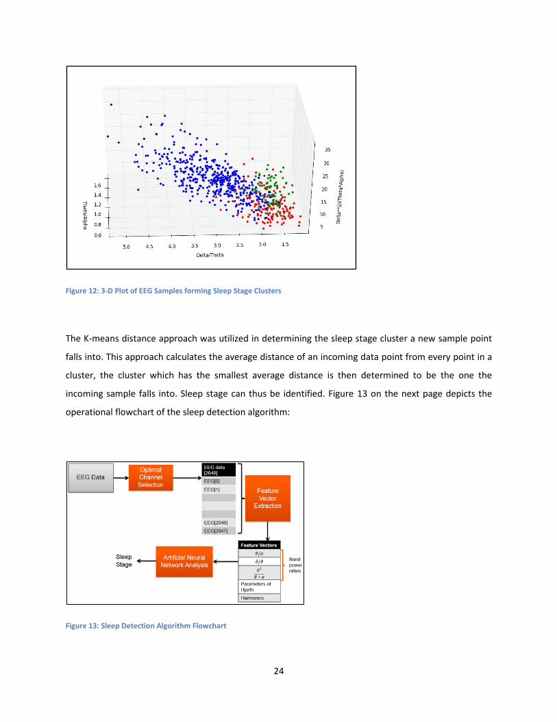
24
Figure 12: 3-D Plot of EEG Samples forming Sleep Stage Clusters
The K-means distance approach was utilized in determining the sleep stage cluster a new sample point
falls into. This approach calculates the average distance of an incoming data point from every point in a
cluster, the cluster which has the smallest average distance is then determined to be the one the
incoming sample falls into. Sleep stage can thus be identified. Figure 13 on the next page depicts the
operational flowchart of the sleep detection algorithm:
Figure 13: Sleep Detection Algorithm Flowchart

25
The algorithm code in Python can be found in section “” of the appendix.
The sleep stage detection algorithm was tested using 15 sets of pre-scored EEG data obtained from
http://physionet.org/physiobank/database/capslpdb/ sleep database, each measured over the course of
a night’s sleep, as learning data.
The sleep stage annotations for the datasets were modified to combine sleep stages 1 and 2 (light
sleep), and stages 3 and 4 (deep sleep). The reason being we only require distinguishing between light
and deep sleep to optimize waking, and are not concerned with the type of light or deep sleep. Thus, 4
clusters were defined as follows:
1. REM.
2. Light Sleep.
3. Deep Sleep.
4. Awake.
The algorithm was then tested using a pre-scored EEG dataset to calculate the sleep stage for each
sample. The results were then compared to the scored sleep stages at the time interval for each sample
to check for accuracy. The number of agreements between the sleep researchers’ and algorithm’s
scored sleep stages were calculated, and an accuracy of 50% was achieved.
However, a large number of the discrepancies occurred between distinguishing REM and light sleep. This
is unsurprising as REM sleep shares many common attributes to light sleep, such as high frequency brain
activity. Despite the similarities between REM and light sleep, it is found that waking someone during
REM sleep results in a high level of lethargy during the day.

26
We also tested the following machine learning algorithms (from the Scikit-learn python library:
http://scikit-learn.org/stable/) to classify sleep stages on future EEG data sets: support vector machine,
stochastic gradient descent, decision tree, random forest, Ada boost, and naive Bayes. However, we
were not able to achieve any better accuracy. The results are shown in Table 2 below:
Table 2: Results of Sleep Detection Algorithm
Processing
Support
vector
machine
Stochastic
gradient
descent KPCA
Decision
trees
Random
forest Ada boost
Naive
Bayes
REM vs. all 0 1.171875 63.28125 60.9375 35.546875 84.765625 51.171875
REM+1 vs. 2
vs. 3+4 32.421875 0.78125 31.25 30.859375 38.671875 30.859375 33.984375
REM vs. 1+2
vs. 3+4 32.421875 0.78125 49.90625 33.203125 25 30.859375 33.984375
No post
processing 32.421875 0.78125 31.640625 21.484375 18.359375 30.859375 2.734375
Thus, the algorithm is actually highly unreliable in optimizing sleep if it cannot distinguish REM from light
sleep. We learned from EEG sleep scoring literature that secondary signals from Electrocardiography
sensors are often required to distinguish the two stages of sleep. A future area of development for this
project is the introduction of a second type of sensor which serves to measure a control signal to further
increase the accuracy of detecting user sleep stages.

27
Bluetooth Wireless Transmission Module
Our Android Application is compiled with API 19: Android 4.4 (KitKAt). The target SDK is API 19: Android
4.4 (KitKAt) and the minimum required SDK is API 8: Android 2.2 (Froyo). Android SDK is the Android
software development kit which uses XML to define layouts and Java to define logic. More information
can be found on the Android developer’s website: http://developer.android.com/index.html.
We utilized source code found on the Android developers’ website:
http://developer.android.com/guide/topics/connectivity/bluetooth.html. Particularity, we implemented
source code for discovering Bluetooth devices, querying paired devices, initializing and managing the
Bluetooth connection.
Our Android application references the GraphView 3.0 library. GraphView 3.0 has many features that
are relevant to our programing need; notably GraphView 3.0 can draw multiple series of data in real-
time. More information can be found on their website: http://android-graphview.org/.
Our Android application is composed of two activities and two layouts. Our main activity is launched on
startup. The view is set to activity_main.xml, where our graphing interface is located. Our GraphView 3.0
associated variables are initialized in the init() method and our button associated variables are initialized
with buttonInit().
Figure 14

28
Our buttons use the onClick(View v) method. The view is set to activity_bluetooth.xml. When the
“Connect” button is pressed, the application starts the Bluetooth activity. Bluetooth activity checks to
see if the Android device the application is being run on is a Bluetooth enabled device. The
startDiscovery() and getPairedDevices() methods (defined by source code from the developer’s site)
then populate the listview and check for paired devices respectively.
Figure 15
When a paired device in the listview is clicked, the private class ConnectThread is called; ConnectThread
is responsible for initializing the Bluetooth connection. Upon successfully connecting, it sends a message
(tagged as SUCCESS_CONNECT) to the message handler (defined in MainActivity.java and imported into

29
Bluetooth.java) which in turn calls the private class ConnectedThread; ConnectedThread reads the
inputStream and sends a message (tagged as MESSAGE_READ) to the same message handler which in
turn parses the data, graphs it, and appends it to the config.txt file via the writeToFile(String s) method.
Figure 16
Unfortunately a few features were left out due to time pressure – in its current iteration the app merely
exists to prove the concept. Future iterations will be able to parse multiple sets of incoming data and
graph them simultaneously or separately. Also, the actual alarm algorithm (written in Python) has not
been ported into the app yet but will be done with by implementing Jython.

30
Bill of Materials
Part Supplier Part # URL
AD620AN Digikey AD620AN http://www.digikey.com/product-
detail/en/AD620AN/AD620AN-ND/612051
LM741CN Digikey LM741CN http://www.digikey.com/product-
detail/en/LM741CN/LM741CN-ND/3701401
Electrode Biopac EL120 http://www.biopac.com/silver-silver-chloride-post-
electrode
Shielded
wire
Radio Shack CL2X http://www.radioshack.com/product/index.jsp?produc
tId=2062643&znt_campaign=Category_CMS&znt_sourc
e=CAT&znt_medium=RSCOM&znt_content=CT2032227
560 Ω
resistor
Digikey CFR-25JR-52-
560R
http://www.digikey.com/product-detail/en/CFR-25JR-
52-560R/560QTR-ND/11968
5 kΩ
resistor
Digikey RNF 1/4 T9 5K
0.1% R
http://www.digikey.com/product-
detail/en/RNF%201%2F4%20T9%205K%200.1%25%20R
/RNF1%2F4T95KBR-ND/1682715
1 kΩ
resistor
Digikey CFR-25JR-52-1K http://www.digikey.com/product-detail/en/CFR-25JR-
52-1K/1.0KQTR-ND/11974
8.2 MΩ
resistor
Digikey HHV-25JR-52-
8M2
http://www.digikey.com/product-detail/en/HHV-25JR-
52-8M2/8.2MAATR-ND/2058731
1 MΩ
resistor
Digikey CFR-25JR-52-
1M
http://www.digikey.com/product-detail/en/CFR-25JR-
52-1M/1.0MQTR-ND/12046
4.3 nF
capacitor
Digikey SA305A432JAA http://www.digikey.com/product-
detail/en/SA305A432JAA/SA305A432JAA-ND/1548877
800 pF
capacitor
Mouser 661-
EKY80ELL801M
M25S
http://www.mouser.com/ProductDetail/United-Chemi-
Con/EKY-
800ELL801MM25S/?qs=sGAEpiMZZMsh%252b1woXyU
Xj6XsRI28M3lIet3CBBRwRDA%3d
Arduino
Mini Pro
Sparkfun DEV-11113 https://www.sparkfun.com/products/11113
31
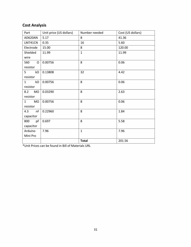
Cost Analysis
Part Unit price (US dollars) Number needed Cost (US dollars)
AD620AN 5.17 8 41.36
LM741CN 0.35 16 5.60
Electrode 15.00 8 120.00
Shielded
wire
11.99 1 11.99
560 Ω
resistor
0.00756 8 0.06
5 kΩ
resistor
0.13808 32 4.42
1 kΩ
resistor
0.00756 8 0.06
8.2 MΩ
resistor
0.03290 8 2.63
1 MΩ
resistor
0.00756 8 0.06
4.3 nF
capacitor
0.22960 8 1.84
800 pF
capacitor
0.697 8 5.58
Arduino
Mini Pro
7.96 1 7.96
Total 201.56
*Unit Prices can be found in Bill of Materials URL

32
Conclusion
To sum up, currently, FortyWinks is focused on completing product development and initiating the
commercial release of the Hypnolarm system. To date, we have raised $20,000 in seed capital from
private investors and are currently approaching angel investment groups, technology incubators, and
venture capital firms to secure additional funds. This process can be expected to reach an initial goal by
the end of 2014.
Future generations of the Hypnolarm system will be progressively more advanced. We plan on
implementing deep sleep stimulation, which can enhance memory, cognition, and possibly productivity,
in our next iteration. With time, Hypnolarm will evolve from a sleep optimization system into a complete
wellness system with potential for medical, military, and other applications. For now, we remain
completely focused on our initial commercial launch.
We have finished proof-of-concept, and within the next year our goal is to build a beta prototype and
send it for product optimization. The beta prototype will have enhanced bio-signal acquisition, more
accurate sleep stage determining, and include the accompanying sleep optimization app. We are seeking
capital to progress from proof-of-concept to significant market penetration. With the increasing
opportunistic wellness/wearables technology market, we will create a productivity niche in this booming
market and set the wheels in motion for the success of FortyWinks, the lifestyle technology brand.
FortyWinks. Sleep less, do more.

33
References
[1] Patricia Tassi and Alain Muzet, “Sleep Inertia,” Sleep Medicine Reviews, vol. 4, 2000.
[2] Cah6, “DIY EEG Circuit,” http://www.instructables.com/id/DIY-EEG-and-ECG-Circuit/?ALLSTEPS
[3] “Sallen–Key topology,” http://en.wikipedia.org/wiki/Sallen%E2%80%93Key_topology
[4] Ferrara, Michele, and Luigi De Gennaro. "How much sleep do we need?." Sleep Medicine Reviews
5.2 (2001): 155-179.
[5] Tassi, Patricia, and Alain Muzet. "Sleep inertia." Sleep Medicine Reviews 4.4 (2000): 341-353.
[6] Giganti, Fiorenza, et al. "Body movements during night sleep and their relationship with sleep stages
are further modified in very old subjects." Brain Research Bulletin 75.1 (2008): 66-69.
[7] Markov, Dimitri, and Marina Goldman. "Normal sleep and circadian rhythms: neurobiological
mechanisms underlying sleep and wakefulness." Psychiatric Clinics of North America 29.4 (2006):
841-853.
34
Appendix
Figure 17: 2nd
order low pass filter
Figure 18: Summing circuit

35
Figure 19: Low pass filter frequency response data points
LPF Response
Frequency (Hz) Vin (mV) Vo (mV) Vo/Vin Gain(dB)
1 480.92 474.15 0.985923 -0.12314
5 480.34 473.38 0.98551 -0.12678
10 481.92 469.32 0.973855 -0.23012
20 482.69 425.09 0.880669 -1.10375
30 482.4 324.05 0.671745 -3.45591
40 480.66 223.63 0.465256 -6.64616
50 480.4 155.77 0.324251 -9.78238
60 482.33 112.51 0.233264 -12.6431
70 483.43 84.57 0.174937 -15.1423
80 481.46 66.05 0.137187 -17.2537
90 481.08 52.72 0.109587 -19.2048
100 481.69 43.3 0.089892 -20.9256
150 482.24 20.24 0.041971 -27.5411
200 480.43 12.4 0.02581 -31.7642
500 481.5 4.06 0.008432 -41.4814
1000 479.31 2.96 0.006176 -44.1865

36
Figure 20: Complete circuit frequency response
Figure 21: Complete circuit frequency response data points
0
5
10
15
20
25
30
35
40
1 10 100 1000
Gain(dB)
Frequency(Hz)
Complete Circuit Frequency Response
Series1
Complete Circuit Response
Frequency (Hz) Vin (mV) Vo (mV) Vo/Vin Gain(dB)
1 17.84 1087 60.93049 35.69669
5 20.02 1061 52.997 34.48503
10 17.77 1036 58.30051 35.31345
20 18.49 937.91 50.72526 34.10449
30 17.93 729.72 40.69827 32.19152
40 16.9 504.14 29.83077 29.49329
50 17.57 354.07 20.15196 26.08635
60 18.8 270.34 14.37979 23.15505
70 17.5 195.79 11.188 20.97505
80 17.99 161.82 8.994997 19.08002
90 17.93 140.89 7.85778 17.906
100 17.59 103.05 5.858442 15.35564
150 16.87 53.78 3.187908 10.07011
200 18.68 48.95 2.62045 8.367516
500 18.15 33.17 1.827548 5.237377
1000 19.28 22.7 1.177386 1.418377

37
AD620AN datasheet
http://www.analog.com/static/imported-files/data_sheets/AD620.pdf
LM741CN datasheet
http://www.ti.com/lit/ds/symlink/lm741.pdf
Biopac EEG electrode specification sheet
http://www.biopac.com/Product_Spec_PDF/EL120.pdf
Arduino Mini Pro Schematic
http://arduino.cc/en/uploads/Main/Arduino-Pro-Mini-schematic.pdf