Embed Size (px)
Citation preview

HAL Id: hal-00410135https://hal.archives-ouvertes.fr/hal-00410135
Submitted on 17 Aug 2009
HAL is a multi-disciplinary open accessarchive for the deposit and dissemination of sci-entific research documents, whether they are pub-lished or not. The documents may come fromteaching and research institutions in France orabroad, or from public or private research centers.
L’archive ouverte pluridisciplinaire HAL, estdestinée au dépôt et à la diffusion de documentsscientifiques de niveau recherche, publiés ou non,émanant des établissements d’enseignement et derecherche français ou étrangers, des laboratoirespublics ou privés.
WDDL is Protected Against Setup Time ViolationAttacks
Nidhal Selmane, Shivam Bhasin, Sylvain Guilley, Tarik Graba, Jean-LucDanger
To cite this version:Nidhal Selmane, Shivam Bhasin, Sylvain Guilley, Tarik Graba, Jean-Luc Danger. WDDL is ProtectedAgainst Setup Time Violation Attacks. CHES, Sep 2009, Lausanne, Switzerland. pp.73-83, 2009,<10.1109/FDTC.2009.40>. <hal-00410135>

WDDL is Protected Against Setup Time Violation Attacks
Nidhal Selmane, Shivam Bhasin, Sylvain Guilley, Tarik Graba, Jean-Luc Danger
Institut TELECOM, TELECOM ParisTech, CNRS LTCI (UMR 5141)
Departement COMELEC, 46 rue Barrault
75 634 PARIS Cedex 13, FRANCE
Email:{selmane,bhasin,guilley,graba,danger}@telecom-paristech.fr
Abstract—In order to protect crypto-systems against sidechannel attacks various countermeasures have been imple-mented such as dual-rail logic or masking. Faults attacksare a powerful tool to break some implementations of robustcryptographic algorithms such as AES and DES. Various kindof fault attacks scenarios have been published. However, veryfew publications available in the public literature detail thepractical realization of such attacks. In this paper we presentthe result of a practical fault attack on AES in WDDL andits comparison with its non-protected equivalent. The practicalfaults on an FPGA running an AES encryptor are realized byunder-powering it and further exploited using Piret’s attack.The results show that WDDL is protected against setupviolation attacks by construction because a faulty bit is replacedby a null bit in the ciphertext. Therefore, the fault leaks noexploitable information. We also give a theoretical model forthe above results. Other references have already studied thepotential of fault protection of the resynchronizing gates (delay-insensitive). In this paper, we show that non-resynchronizinggates (hence combinatorial DPL such as WDDL) are nativelyimmune to setup time violation attacks.
Keywords-AES; FPGA; Setup violation fault attacks;WDDL; Protection against faults.
I. INTRODUCTION
Side channel analysis or attacks (SCA) are attacks based
on the analysis of the secret information (generally the
encryption key) leaked from the physical implementation of
the cryptographic system. The leakage is passively observed
via timing information, power consumption, electromagnetic
radiations, etc. Protection against side channel attacks is
important because the attacks can be implemented quickly
and at a low cost. Differential power analysis (DPA) [1] and
its derivatives such as correlation power analysis (CPA) [2]
correlate the leakages with an internal power model, which
depends on the cryptographic key.
Several countermeasures have been devised to avoid
SCA. Dual-rail with precharge logic (DPL) is one of the
state-of-the-art countermeasure against SCA. In DPL, the
idea is to make the power consumption of the device
uniform, thus hiding the crucial information it conceals.
Each signal is replaced by true and false representations.
Precharge & Evaluation phases are alternated to ensure
exactly one switching event per cycle. Wave Dynamic
Differential Logic (WDDL) [3] is one of the commonly
used DPL. Unlike Sense Amplifier based Logic (SABL) [4],
WDDL uses standard CMOS cells. Owing to this property,
WDDL can be used with any design as no special library
is required. Due to the same reason it can be used in
FPGAs [5], [6]. It is interesting to note that WDDL is
prone to the “early evaluation” vulnerability [7], corrected
from instance in SecLib [8], [9]. Despite this second-order
issue, WDDL is relatively secure for a reasonable overhead.
Hereafter we present our work with respect to WDDL
designs.
Differential fault attacks (DFA) [10], [11], [12] also
referred to as active attacks alter the functional behavior
of the attacked device by injecting one or several faults.
Several techniques are available to inject faults: variations of
the supply voltage or clock frequency, temperature variation
or irradiation by a laser beam which leads to a wrong
computation result that can be exploited to perform DFA.
Some countermeasures for DFA have been introduced. These
countermeasures are generally based on temporal [13] or
spatial [14], [15] redundancy, either in a generic manner or
taking advantage of some peculiarity of the algorithm.
Here in this paper we analyze the security of WDDL
against setup violation fault attacks. We implemented AES
(Singlerail & WDDL). Singlerail refers to simple version
of AES and WDDL the DPL version. The sbox of the AES
is implemented by calculations in composite field GF(24)as described in [16].
The results presented in this article are obtained with
an EP1S25 Altera Stratix FPGA soldered on a Parallax
evaluation board. As described in [17], [18], faults can
practically be induced in an FPGA by under-powering the
circuit. When we drive the FPGA at a voltage less than the
nominal voltage, the propagation time of the signal increases
as illustrated in figure 1. Such attacks are non-invasive in
nature as the attacker does not need access to the silicon
die and are therefore easy to implement. We recall that
there is no straightforward mechanism to monitor either the
power supply level or the frequency in commodity FPGAs.
The permanent under-powering causes a phenomenon called
“setup time violation” on one of the timing path of the design
causing a faulty byte. We call this fault as a “byte-flip” fault,
which is obtained by flipping of one or more bits in a byte.
The number of bits flipped during a byte-flip is called the
Hamming weight of the fault. Since cryptography involves

highly complex computations it is very likely that the critical
path is in the cryptographic part [19]. Such faults can be
exploited using various known attacks [20], [21], [22]. Here
we use Piret’s attack to exploit the faults and retrieve the
secret key using the method described in [20].
Setup violatedSetup met
Q’
QD
Q’
QD
clk clk
V cc ↓ ⇒ Tpropagation ↑
Figure 1. Setup violation.
The rest of the paper is organized as follows. In section II,
we explain the WDDL rationale and the design flow to
implement it. Section III describes the attack setup and the
faults analysis procedure. Section IV presents the compari-
son of a fault acquisition campaign on single-rail and WDDL
version of AES, in terms of spatio-temporal localization of
faults. Section V is devoted to the theoretical demonstration
of the intrinsic immunity of WDDL against setup violation
attack on AES. Finally, the section VI concludes the paper
and opens perspectives for better protecting sensitive cryp-
tographic implementations.
II. WAVE DYNAMIC DIFFERENTIAL LOGIC
Power consumption of a standard CMOS cell is dependent
on the transition of its input. Thus for a DPA-resistant
design, a possible solution could be to introduce a family of
DPA resistant cells. In a WDDL cell [3], one transition per
cycle is observed, which is favourable for a DPA resistant
logic style.
WDDL uses true and false representations of each signal
(I/O of each cell). To make the power consumption fairly
uncorrelated to the processed data, it is necessary that there
should be the same number of transition every cycle. This
condition is fulfilled by alternate cycles of precharge and
evaluation. In the precharge phase all the signals are charged
to the same level (e.g. 0 in WDDL) and during evaluation
exactly one of the two complementary outputs is evaluated
(=1). Figure 2 shows the timing diagram of WDDL AND
gate. We can see that during precharge all signals are
put to logic 0. During evaluation, exactly one of the two
complementary inputs and outputs evaluates to 1.
In DPL, glitches make the design vulnerable to at-
tacks [23]. Indeed, without special attention, if the inputs
arrive at different moments, glitches can be observed. To
avoid glitches it is necessary that all the gates in the design
Precharge Evaluation
bt
yt
bf
yf
af
at
PRE/EV AL
Figure 2. Timing diagram for a WDDL AND gate.
should be positive in nature. To ensure this in WDDL,
the design is synthesized with a library consisting of only
positive gates (like AND, OR) [24]. As shown in figure 3,
a WDDL AND gate consists of an AND gate (G) and a
complementary OR gate (G∗, satisfying G∗(x).= G(x)).
For sequential circuits, each flip-flop is replaced by a pair
a flip-flops. This double flip-flop allows the precharge wave
to propagate through the whole design as all the gates are
positive. It has to be noted that inverters in WDDL are
implemented by crossing the true and false signals of the
same variable.
A point worth noting in figure 3 is that one flip-flop in the
single-rail design is replaced by four flip-flops in the WDDL
design. This is explained as follows. During the precharge
phase, the combinatorial part of the circuit will be discharged
to 0 and this 0 is stored to the first of the two flip-flops. The
second flip-flop will store the result of the last computation.
In the evaluation phase, the value stored in the second flip-
flop serves as input and the output is stored in the first flip-
flop. In the mean while, the zero stored in the first flip-flop
is shifted to the second flip-flop to allow proper precharge
of the circuit ahead in the next cycle. This phenomenon
happens in both true and false rail. Thus the number of flip-
flops is quadrupled in the WDDL design.
G
G
Single−rail
Dual−rail
QB
A
Qf
QtBt
At
Af
Bf G∗
Figure 3. WDDL building block.
In our implementation, we use a different way to ensure
all positive logic. Instead of using positive gates, we use a
library containing all look-up tables (LUTs) which imple-
ment a positive function. This technique is called WDDL+
in [25].
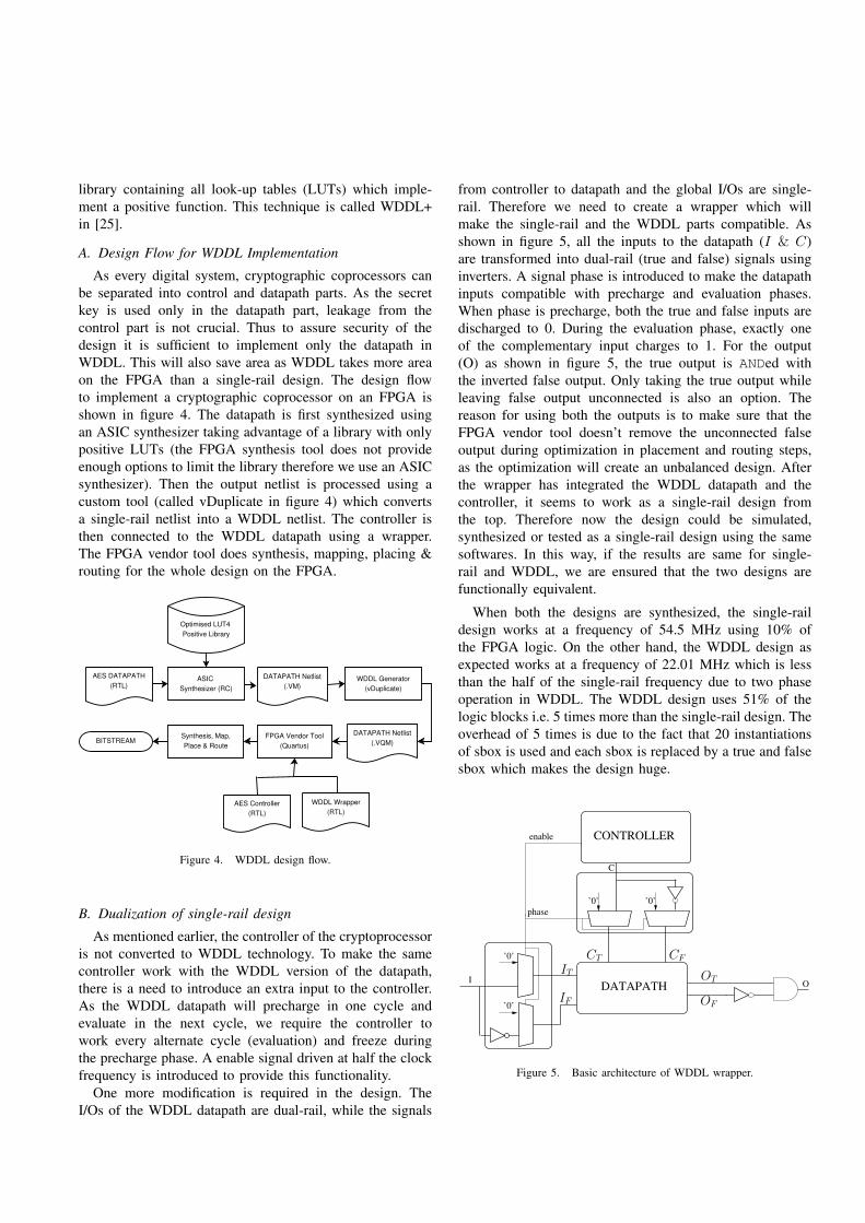
A. Design Flow for WDDL Implementation
As every digital system, cryptographic coprocessors can
be separated into control and datapath parts. As the secret
key is used only in the datapath part, leakage from the
control part is not crucial. Thus to assure security of the
design it is sufficient to implement only the datapath in
WDDL. This will also save area as WDDL takes more area
on the FPGA than a single-rail design. The design flow
to implement a cryptographic coprocessor on an FPGA is
shown in figure 4. The datapath is first synthesized using
an ASIC synthesizer taking advantage of a library with only
positive LUTs (the FPGA synthesis tool does not provide
enough options to limit the library therefore we use an ASIC
synthesizer). Then the output netlist is processed using a
custom tool (called vDuplicate in figure 4) which converts
a single-rail netlist into a WDDL netlist. The controller is
then connected to the WDDL datapath using a wrapper.
The FPGA vendor tool does synthesis, mapping, placing &
routing for the whole design on the FPGA.
AES DATAPATH
(RTL)ASIC
Synthesizer (RC)
DATAPATH Netlist
(.VM)WDDL Generator
(vDuplicate)
DATAPATH Netlist
(.VQM)FPGA Vendor Tool
(Quartus)
AES Controller
(RTL)
Synthesis, Map,
Place & RouteBITSTREAM
WDDL Wrapper
(RTL)
Optimised LUT4
Positive Library
Figure 4. WDDL design flow.
B. Dualization of single-rail design
As mentioned earlier, the controller of the cryptoprocessor
is not converted to WDDL technology. To make the same
controller work with the WDDL version of the datapath,
there is a need to introduce an extra input to the controller.
As the WDDL datapath will precharge in one cycle and
evaluate in the next cycle, we require the controller to
work every alternate cycle (evaluation) and freeze during
the precharge phase. A enable signal driven at half the clock
frequency is introduced to provide this functionality.
One more modification is required in the design. The
I/Os of the WDDL datapath are dual-rail, while the signals
from controller to datapath and the global I/Os are single-
rail. Therefore we need to create a wrapper which will
make the single-rail and the WDDL parts compatible. As
shown in figure 5, all the inputs to the datapath (I & C)
are transformed into dual-rail (true and false) signals using
inverters. A signal phase is introduced to make the datapath
inputs compatible with precharge and evaluation phases.
When phase is precharge, both the true and false inputs are
discharged to 0. During the evaluation phase, exactly one
of the complementary input charges to 1. For the output
(O) as shown in figure 5, the true output is ANDed with
the inverted false output. Only taking the true output while
leaving false output unconnected is also an option. The
reason for using both the outputs is to make sure that the
FPGA vendor tool doesn’t remove the unconnected false
output during optimization in placement and routing steps,
as the optimization will create an unbalanced design. After
the wrapper has integrated the WDDL datapath and the
controller, it seems to work as a single-rail design from
the top. Therefore now the design could be simulated,
synthesized or tested as a single-rail design using the same
softwares. In this way, if the results are same for single-
rail and WDDL, we are ensured that the two designs are
functionally equivalent.
When both the designs are synthesized, the single-rail
design works at a frequency of 54.5 MHz using 10% of
the FPGA logic. On the other hand, the WDDL design as
expected works at a frequency of 22.01 MHz which is less
than the half of the single-rail frequency due to two phase
operation in WDDL. The WDDL design uses 51% of the
logic blocks i.e. 5 times more than the single-rail design. The
overhead of 5 times is due to the fact that 20 instantiations
of sbox is used and each sbox is replaced by a true and false
sbox which makes the design huge.
’0’’0’
’0’
’0’
OI
C
phase
DATAPATH
CONTROLLERenable
OT
CFCT
IF
IT
OF
Figure 5. Basic architecture of WDDL wrapper.

III. SETUP FOR FAULT ATTACKS ON FPGAS
In order to induce faults during the execution of the
algorithm we drive the core of the FPGA at a non-nominal
continuous voltage V cc. The power supply is remotely
controlled using GPIB cable.This feature allows us to test
various values of input voltage successively. For each value
of V cc, the triples {message, key, ciphertext} are recorded
for 1,000 encryptions at each 100 values of V cc. Figure 6
sketches the experimental setup. The testing platform is a
stratix FPGA soldered on a parallax board. The FPGA is
powered by the progarammable power supply. The rest of
the board is powered by a 5V constant supply.
RS232
GPIBV cc
Figure 6. Experimental platform.
Once acquisition is done, we use a software for an offline
analysis of the collected ciphertext in order to detect single
byte errors that occur during the encryption. A modified
RTL description of AES where faults can be injected at
any byte of the ten rounds is used to generate a dynamic
database. The database consists of all possible ciphertexts
generated only by single faults for each key, message pair.
Then we test if the faulty ciphertext matches an entry in the
database. If so, the fault is said “covered” otherwise the fault
is said “uncovered” and the ciphertext is affected by multiple
byte faults. If a fault is covered, the software provides the
location, the value of the faulty byte, its corresponding
correct byte and the Hamming weight of the fault. The
purpose of this implementation is to identify the typology
of single faults that occurs in the FPGA.
If the fault is ”covered” then we can identify the round
and the sbox affected by the fault. This concludes that the
voltage reduction generates random single faults that most
differential attack models are based on. In this experiment
we use a global non-invasive fault injection technique. The
propagation time increases with the decrease of the power
supply and faults are caused by an early latching of a
combinatorial function as shown in figure 1.
IV. EXPERIMENTAL RESULTS
In this section, the fault analysis is used to find the
occurrence of a single byte fault that affects the state matrix
of AES. Both single-rail and WDDL versions are tested
against setup violation faults. Faults detected are those
occurring only in the datapath, while the key schedule is
assumed here to be fault-free. Indeed, in our design, the key
schedule block is not critical in timing.
Figure 7a shows the occurrence of faults in single-rail
implementation. We can see that the graph of single faults
has a bell-shaped distribution. As we decrease the voltage
beyond a certain threshold, setup time is violated on multiple
paths and faults become multiple (uncovered). The max-
imum percentage of single faults is 39% at a voltage of
1.256 V as shown in figure 7a. All single faults are analyzed
in terms of spatio-temporal locality: Figure 8a and figure 9a.
26% of single faults occur in round 8 and 12% of them occur
in round 9 (refer figure 8a). Such faults are exploitable using
Piret’s Attack. Thus the single-rail implementation of AES
with SBOX in LUT is not protected against “setup violation”
attacks.
For the WDDL version of AES, the results are shown in
the figure 7b. Since we use only positive LUTs to implement
WDDL, there are no glitches in the circuit. When we run
the fault attack campaign on WDDL design, less than 2%of the detected faults are single and all of them fall in the
last round of AES as shown in figure 8b. These faults are
not exploitable and thus the key cannot be retrieved using
Piret attack. The software for fault analysis allows us to see
faulted bytes and its corresponding correct value (value of
byte if not faulted). We find that everytime a fault occurs,
the faulted value C∗ is less than its corresponding correct
value C, in a bitwise sense: C & C∗ = C∗. This comes
down to using the partial order �, defined bit by bit in the
following truth table:
C C∗ C∗ � C
0 0 1
0 1 0
1 0 1
1 1 1
This means that all the faults are caused when an expected
‘1’ takes a value equal to ‘0’.
The reason why all the faults are seen in the last round
is as follows. When an XOR gate is implemented using

positive logic, it is a combination of AND, OR gates
and inverters (for inverted inputs). These inverters yield a
mixture of true and false part of the design as per the
definition of XOR. Thus a fault occurring in a true part
is further corrupted by mixing with the false part and
vice versa. The MixColumns operation involves a lot of
XOR operations. Therefore a MixColumns operation after a
fault will corrupt the fault which cannot be detected. Since
the last round does not have MixColumns, the faults are
detected but not exploitable. One interesting observation was
that every time a byte is affected by a fault, a null byte
in the ciphertext was reflected at its expected place. This
means that even after successfully injecting the fault during
encryption and precisely knowing the location of the fault,
the output does not give any information which can be acted
upon to retrieve the hidden secrets. The results observed are
easily reproducible. This means that for a particular voltage
lower than the nominal voltage, if the ciphertext and input
message are constant, the fault is often in the same sbox.
This feature gives us better flexibility for complete analysis
of these faults. Therefore, a WDDL design is naturally
secure against setup violation faults. This has been further
explained in the section V-A.
V. THEORETICAL FAULT ANALYSIS
The purpose of this section is to show that the fault model
corresponding to a setup violation time has the consequence
that all DFAs on AES in WDDL are impractical.
A. Fault Analysis on AES in WDDL with SubBytes in LUTs
1) Fault Model: In an under-powering or overclocking
attack, faults arise from a setup time violation [17], [18].
Authors of paper [26] argue that the effect of a glitch on
the power supply increases the propagation times of all the
signals, which makes this disturbance similar in effect to the
global chip under-powering. As the WDDL protocol with a
(0, 0) spacer starts in evaluation step with all the nodes
voltage equal to zero, the evaluation consists in propagating
rising transitions along exactly half of the wires. If by any
means, an attacker manages to trigger a setup time violation,
the consequence is an asymmetric bit flip: only 1 to 0 errors
are considered. Therefore, the consequence of the fault is to
leave (at least) one dual-rail signal in its (0, 0) precharge
state, while the others couples of wire are in legal (0, 1) or
(1, 0) evaluation state.
As already discussed in Sec. IV, the error is likely to
happen for a few dual-rail signals if the stress level is low.
This invalid data representation will then propagate through
the next round logic. Four cases are possible:
1) the protocol error can turn into functional errors on
the data or not, and
2) the protocol errors can vanish while flowing through
the combinatorial logic (self protocol healing), or, at
the opposite, be amplified.
Table IMODIFIED FUNCTIONALITY OF AN AND GATE IN THE PRESENCE OF
ERASURE FAULTS.
Correct computation
a b at af bt bf ct cf c
0 0 0 1 0 1 0 1 0
0 1 0 1 1 0 0 1 0
1 0 1 0 0 1 0 1 0
1 1 1 0 1 0 1 0 1
Faulted computation
a b at af bt bf ct cf c
NULL 0 0 0 0 1 0 1 0
NULL 1 0 0 1 0 0 0 NULL
Table IIMODIFIED FUNCTIONALITY OF AN XOR GATE IN THE PRESENCE OF
ERASURE FAULTS.
Faulted computation
a b at af bt bf ct cf c
NULL 0 0 0 0 1 0 0 NULL
NULL 1 0 0 1 0 0 0 NULL
The next section shows that functional errors occur, cor-
responding to bits erasure. In addition, the erasure rate
increases: one single error at the entrance of a round will
trigger many invalid precharge bits to be generated, and
we show that in a reasonable cryptographic algorithm (no
computation is done uselessly), the erasure rate increases.
The consequence is that, after some percolation in the
combinatorial logic, most of the values are erased.
2) Propagation of Faults: We start this analysis by the
example of two representative gates: the AND and the XOR
functions each having two inputs that we note a and b. We
assume in this study that the fault occurs on input a. In
evaluation, instead of having (at, af ) = (0, 1) when a =0 and (at, af ) = (1, 0) otherwise, we simply have at =af = 0, which can also be expressed as a=NULL. The logic
that implements the AND gate is (ct, cf ) = (at · bt, af +bf ). When a is faulty, the Tab. I function degenerates to
AND(a∗, b) = 0 if b = 0, and NULL otherwise.
The same analysis can be carried out for the WDDL XOR
gate in figure 10. The logic that implements the WDDL XOR
gate is (ct, cf ) = (at · bf +af · bt, (af + bt) · (at + bf )). This
equation shows that if we have a faulty input (at = af = 0)then the output will be NULL (ct = cf = 0) . Thus the
XOR gate has a maximum error propagation since the error
is propagated for any value of b as shown in table II.
Now, for any function f , we have this property:
Definition Let f be a positive Boolean function with inputs

0
20
40
60
80
100
1230 1240 1250 1260 1270 1280
Occu
rre
nce
[%
]
Voltage [mV]
Majority ofsingle errors
Majority ofmultiple errors
FaultsSingle errors
Multiple errors
Figure 7a. Occurrence of Fault — Singlerail.
0
10
20
30
40
50
60
70
80
90
100
1900 1910 1920 1930 1940 1950 1960
Occu
rre
nce
[%
]
Voltage [mV]
FaultsSingle errors
Multiple errors
Figure 7b. Occurrence of fault — WDDL.
0
5
10
15
20
25
30
R10
R9
R8
R7
R6
R5
R4
R3
R2
R1
% o
f fa
ults
Round
Temporal localization
Figure 8a. Temporal localisation — Singlerail.
0
20
40
60
80
100
R10
R9
R8
R7
R6
R5
R4
R3
R2
R1
% o
f fa
ults
Round
Temporal localization
Figure 8b. Temporal localization of fault — WDDL.
0
5
10
15
20
25
30
35
40
S15
S14
S13
S12
S11
S10
S9
S8
S7
S6
S5
S4
S3
S2
S1
S0
% o
f fa
ults
Sbox
Spatial localization
Figure 9a. Spatial localisation — Singlerail.
0
5
10
15
20
25
30
35
40
45
50
S15
S14
S13
S12
S11
S10
S9
S8
S7
S6
S5
S4
S3
S2
S1
S0
% o
f fa
ults
Sbox
Spatial localization
Figure 9b. Spatial localization of fault — WDDL.

True
FalseCf
Bf
Af
Bt
At
Ct
Figure 10. WDDL implementation of the XOR gate.
(a, b) then its WDDL equivalent F can be defined as:
{
Ft(at, bt) = f(at, bt) ,
Ff (af , bf ) = f(af , bf ) .
The output of f is correct when f does not depend on the
faulty input, and erased otherwise.
The proof is straightforward. If the output does not
depend on the faulty input, the computation is correct for
both the true and the false outputs, because the protocol
violation does not impact the result. On the contrary, for the
configuration of non-faulty inputs b such as F depends on
the faulty input bit, then we have four cases:
1) Ft = Ff = 1: impossible since F is positive and the
inputs are lower than a legal value, that is either (1,
0) or (0, 1),
2) Ft = 1 and Ff = 0. In this case, 1 = f(0, b) [equation
for Ft] and 0 = f(0, b) = f(1, b) [equation for Ff ] ,
i.e. 1 = f(1, b). Therefore f(0, b) = f(1, b). However,
we assumed that F does depend on the first faulty
input, hence a contradiction.
3) Ft = 0 and Ff = 1: for the same reason, this case is
incompatible with the input configuration such that F
does depend on the faulty input.
4) Consequently, the only possibility is that Ft = Ff =0, hence a NULL propagation.
Let us now study a random function, modeling the byte
substitution table (SubBytes) of the AES. If there is a NULL
fault at the input, then:
• for one half of the input data, a specific output bit will
depend on this input, and
• for the other half, the targeted output bit does not
depend on the input.
Therefore, statistically, one half of the output bits are erased
to NULL. Notice that this result is independent of the exact
functional decomposition in a positive dual gates netlist.
Similarly, if two inputs are erased, then 3/4 of the outputs
will also be NULL. And of course, when seven or eight
Table IIIEQUATIONS FOR THE BYTES TRANSFORMATIONS ×01, ×02 AND ×03.
a′ a × 01 a × 02 a × 03
a′
7a7 a6 a7 ⊕ a6
a′
6a6 a5 a6 ⊕ a5
a′
5a5 a4 a5 ⊕ a4
a′
4a4 a3 ⊕ a7 a4 ⊕ a3 ⊕ a7
a′
3a3 a2 ⊕ a7 a3 ⊕ a2 ⊕ a7
a′
2a2 a1 a2 ⊕ a1
a′
1a1 a0 ⊕ a7 a1 ⊕ a0 ⊕ a7
a′
0a0 a7 a0 ⊕ a7
Table IVTRUTH TABLE FOR THE UNIVERSAL GATE AND.
AND ’0’ ’1’ ’U’
’0’ ’0’ ’0’ ’0’
’1’ ’0’ ’1’ ’U’
’U’ ’0’ ’U’ ’U’
errors are presented at the input, all the output bits become
NULL.
We have already shown in section V-A2 that with XOR
gates the fault propagation is maximal. The MixColumns
transformation is a multiplication of a polynomial over
GF (28) with the fixed polynomial a(x)[1], reduced modulo
x4 + 1.
a(x) = (0x03)x3 + (0x01)x2 + (0x01)x + (0x02) (1)
The equations for the byte multiplications involved in this
multiplication are written down in Tab. III. Hence we see
that the MixColumns operation is implemented as a tree of
XOR gates. This ensures a maximum propagation of NULL.
In an SPN (substitution permutation network) like AES,
the fault number can only grow at each step. Indeed,
for every block f , if a fault is stopped, then: f(’U’, x)is certain, for a given input x. Now, this means that
f(’0’, x) = f(’1’, x), and this implies that f is not
bijective. Therefore, differential attacks become difficult as
the attacker observes an erased value, and cannot backtrack
from the faulty ciphertext. The best case being when all the
output bits are erased and thus no information that can be
useful to generate the key is available.
Unlike byte-flips induced by a laser, the setup time
violation on WDDL causes no computation to be wrong.
Instead, when an input is partially NULL, the logic evaluates
the bits that can be correct for sure, but answers NULL if
it cannot decide. Therefore, the propagation model is that
of ’U’ in VHDL [27]. The logic tries to evaluate bits that
would not be wrong if any correct value (’0’ or ’1’) were
used instead of ’U’. We recall in Tab. IV the extended truth
table of the universal gate AND over {’0’,’1’,’U’}2.

xf
xt x
Figure 11. Dual-to-single rail circuitry usable in the case of a NULL0spacer.
As shown in Fig. 11, the conversion of the dual-rail signals
to single-rail turns a NULL into a ’0’. This circuit makes
use of both true and false signal halves, so as to prevent the
CAD tool from simplifying half of the logic and balance the
true and false networks. Therefore, if a fault occurs during
the computation, it can be observed. This difference could
be exploited by an attack, as done in the attack of Gilles
Piret. However, the computed differential will not disclose
any information about the last round key, since the XOR
function used to mix it propagates a NULL.
All the considerations detailed regarding WDDL rely on
the fact the gates are positive. Indeed, the gates will stick
to zero unless valid values are produced. This is not true
for delay insensitive gates which stay in a zero state and
jam the computation. Notice that in WDDL the results are
independent of the type of spacer used. It can be NULL0.=
(0, 0), NULL1.= (1, 1), used as constants or interleaved
alternatively or randomly.
3) Generalization to Arbitrary Fault Models: We con-
sider two categories of faults:
1) Asymmetric faults, where bits can only be flipped
from 1 to 0. This type of faults is typical encountered
in WDDL circuits stressed by a global perturbation,
such as under-voltage or over-clocking. Glitch attacks
can lead to the same symptom, because it manifests
in adding a delay globally to all wires. Flash of white
light have been reported in [28, §12, page 163] to zero
selectively the output of some operations. Equally,
laser shots on SRAM-based FPGAs tend to favor
1 → 0 bit-flips over 0 → 1 [29]. Notice that in DPL
with a (1, 1) spacer, the opposite transition occurs
when trying non-invasive attacks. We do not detail this
situation as it is the exact opposite of the 1 to 0 case.
2) Symmetric faults, where bits are susceptible of tog-
gling in both directions. Laser shots can trigger both
1 to 0 and 0 to 1 transitions. This fault is thus semi-
invasive, as opposed to the previous ones. Therefore,
it models a more powerful attacker, at least able to
chemically prepare the sample to attack.
In the context of asymmetric faults, DPL circuits are
natively protected as such. In this respect, it is interest-
ing to compare the pros and the cons of synchronous
and asynchronous circuits. When exposed to under-voltage,
asynchronous circuits will continue to work, down to a
voltage value where the gates will not be supplied enough
to produce a strong one. Below this threshold, errors of
type ”stuck at zero” will manifest, exactly as in the case
of synchronous circuits. Overclocking is not an attack that
applies to asynchronous circuits that are, by definition,
clockless. However, we have noticed that this perturbation
is ineffective is exposing secrets. Therefore, a synchronous
circuit will be less reliable in the presence of non-invasive
faults, but as secure as an asynchronous circuit. A trade-off
between the two approaches can be reached by considering
synchronous circuits with jitter on the clock. The jitter can
have a large variance, since even if it conducts to a setup
time violation, the secrets remain safe. Therefore, with DPL,
it is secure when used in addition with aggressive clock jitter.
If the attacker has the means to inject symmetric faults,
then three types of protections must be considered:
1) When the fault induction is gentle, single bit flips is the
most likely fault model. In this case, even if the fault
is a 0 to 1 transition occurring during the evaluation
stage, the only risk is to create a (1, 1), also called
NULL1. However, in a dual way of the case study of
the propagation of NULL0 values, we can show that
the propagation of NULL1 consist in an erasure of the
data, so that the syndrome does not convey any single
bit of information about the faulty circuit internal state.
DPL style thus forces the attacker to be less furtive.
2) With a more intense stress, the attacker will start to
induce multiple faults with low multiplicity. In this
case, a DPL gate can output completely false values.
For instance, an AND gate for which the inputs are
NULL0 and NULL1 evaluates to the correct value 0
(with respect to WDDL valid states), even if the two
unfaulty inputs were both equal to 1. To protect the
implementation against those attacks, additional detec-
tion hardware must be added so as to cross-check the
computation. A little gain can however be obtained:
As the DPL style is protected against single faults, a
datapath of n bits can be checked with code words of
only n− 1 bits without risking to weaken the security
level. A protection method at the technological level
such as the one presented in [30] could be extended
from SRAM points to DFFs and combinatorial gates.
By using high-VT P transistors (those that compute the
’1’) and low-VT N transistors (those that compute
the ’0’), the designer could make the faults 1 → 0much more likely than the opposite 0 → 1.
3) When the stress is very strong, then we expect the
faults to be very frequent. Hence the recommendation
to use physical captors spread on the chip surface.
Now, if we consider only asymmetric faults, we could
think that power analysis could be made possible by the
fault injection. Indeed, if DFA does not expose the key, it
at least indicate to the attacker that a fault has happened.
More precisely, we could imagine to correlate the amount
of detected faults to a side-channel, in a view to establish

correlations. Indeed, in nominal operation conditions, the
activity is constant: half of the gates commute in each clock
cycle. When a fault is injected, the activity will become
lower:
• in a fault position dependent fashion (for sure), as
illustrated in Fig. 12,
• but perhaps also in a data dependent fashion.
Time
Time
Fault
Time
Fault
Sid
e-ch
annel
Sid
e-ch
annel
Sid
e-ch
annel
Figure 12. Power dependence of a WDDL circuit in the faults.
However, such an attack cannot be mounted, since if a
sensible variable is faulty, irrespectively of its value, the
fault will generate a NULL0. Therefore, after the fault, the
system has forgotten its value, and computation (in terms
of number of toggles) will continue in similar ways. This
argument is confirmed by the practical observation of power
consumption of WDDL AES as shown in figure 13. We can
see that the power consumption of the device is abruptly
reduced as soon as the fault occurs approximately at time
2130 ps. The power consumption further reduces after two
cycles and remains constant till the end of encryption. It
takes exactly 2 cycles (1 ShiftRows and 2 MixColumns) for
NULL0 to diffuse through the whole design. This holds even
if the DPA protection has a second order flaw, such as early
evaluation. The only way to take advantage of such a flaw
is to exploit it without faults. Indeed, to rephrase why DFA
does not help the DPA, with faults, the distinctions of power
curves at second order simply disappear. We cannot show
any experimental curve to illustrate this point since we have
no mean to deduce the bit concerned with the fault based
on the sole knowledge of the ciphertext.
Finally, we attract the reader’s attention to the fact that
vulnerability analysis of WDDL against faults exploitation
-0.08
-0.06
-0.04
-0.02
0
0.02
0.04
0.06
0.08
0.1
1500 2000 2500 3000 3500 4000 4500
volta
ge
(m
V)
time (ps)
correct
-0.08
-0.06
-0.04
-0.02
0
0.02
0.04
0.06
0.08
0.1
1500 2000 2500 3000 3500 4000 4500
volta
ge
(m
V)
time (ps)
faulty
Figure 13. Practical power consumption of a WDDL circuit in the faults.
or DPA in the presence of faults has been argued in the
precharge to evaluation step. However, it can be transposed
without any change to the case of evaluation to precharge
step. Indeed, the circuit’s behavior is unchanged, except that
0 → 1 transitions are replaced with 1 → 0. And the attacker
has less insight, since he cannot observe the faults occurring
in the precharge stage, that are filtered out by the WDDL
circuit wrapper described in Sec. II-B.
B. Counter-Measures against Non-Invasive Attacks
A straightforward countermeasure against non-invasive at-
tacks on various circuits (not only DPL) consists in inserting
into the circuit some logic in charge of detecting abnormal
situations before the critical parts of the designs become
faulty. For instance, in Fig. 14, a setup consisting of an
even number of inverters between two registers is presented.
The source register invert its value every cycle and the
combinatorial chain of even number of inverters computes
always the same value. At the end of the chain, a destination
register checks that the value computed by the chain. The
setup time of the invertor chain is violated if the monitored
(output) value is different than the input. Hopefully, if the
chain is designed to be longer than the critical path, an alarm
is raised before the cryptographic parts of the design become
faulty.

OI
tchain (2N invertors) > tcrit
1 0 1 00
Monitoring DFF;
I 6= O ⇒ ∃ error
Figure 14. Counter-measure based on the insertion of a monitoring logicwith a propagation time larger than the critical path of the rest of the circuit.
VI. CONCLUSION
Information masking and hiding are two concurrent pro-
tection techniques against side-channel attacks. Last year
at FDTC, Arnaud BOSCHER and Helena HANDSCHUH
showed that masking does not protect against fault at-
tacks [31]. On the contrary, we have demonstrated the-
oretically and shown practically that information hiding
(such as DPL) makes it difficult to mount fault attacks,
since faulty outputs reveal no information about the keys.
Unlike the ”differential behavioral attack” (DBA), where a
simultaneous observation of the faulty message and of the
power curve empowers an attacker into mounting an attack,
in the case of WDDL the attacker cannot learn anything
from power curve corresponding to a faulty encryption.
We show, for the first time, that asymmetric fault attacks
in general being not a threat for DPL circuits. As a perspec-
tive, we can study whether or not more traditional faults
model (such as the byte-flip caused by a laser spot) also
leads to unsuccessful attacks. Provided this analysis turns
out to be correct, all previously proposed countermeasures
against DFA for WDDL would be useless: for instance, the
alarm (namely the (’1’, ’1’) state) propagation scheme
presented in [32] warns of a possible attack against which
the circuit is already natively immune.
ACKNOWLEDGMENTS
The authors would like to acknowledge the support of
French National Research Agency (ANR) SeFPGA https:
//sefpga.enst.fr/ project for this study. Some precious advices
also came from the outputs of the MARS (http://projects.
comelec.enst.fr/mars/) ANR project. Finally, we are very
grateful to the collaboration with STMicroelectronics AST
division (Rousset, France) dealing with hardware crypto-
processors security improvements.
REFERENCES
[1] P. Kocher and J. Jaffe and B. Jun, “Differential PowerAnalysis,” in Proceedings of CRYPTO’99, ser. LNCS, vol.1666. Springer-Verlag, 1999, pp. 388–397.
[2] E. Brier, C. Clavier, and F. Olivier, “Correlation PowerAnalysis with a Leakage Model,” in CHES, ser. LNCS, vol.3156. Springer, August 11–13 2004, pp. 16–29, Cambridge,MA, USA.
[3] K. Tiri and I. Verbauwhede, “A Logic Level Design Method-ology for a Secure DPA Resistant ASIC or FPGA Imple-mentation,” in DATE’04. IEEE Computer Society, February2004, pp. 246–251, Paris, France.
[4] K. Tiri, M. Akmal, and I. Verbauwhede, “A Dynamic andDifferential CMOS Logic with Signal Independent PowerConsumption to Withstand Differential Power Analysis onSmart Cards,” in European Solid-State Circuits Conference(ESSCIRC), September 2002, pp. 403–406, florence, Italy.[Online]. Available: http://citeseer.ist.psu.edu/tiri02dynamic.html
[5] K. Tiri and I. Verbauwhede, “Secure Logic Synthesis,” inFPL, ser. LNCS, vol. 3203, August 2004, pp. 1052–1056.
[6] ——, “Synthesis of Secure FPGA Implementations,” in Inter-national Workshop on Logic and Synthesis (IWLS’04), June2004, pp. 224–231.
[7] D. Suzuki and M. Saeki, “Security Evaluation of DPACountermeasures Using Dual-Rail Pre-charge Logic Style,”in CHES, ser. LNCS, vol. 4249. Springer, 2006, pp. 255–269, http://dx.doi.org/10.1007/11894063 21.
[8] S. Guilley, F. Flament, R. Pacalet, P. Hoogvorst, and Y. Math-ieu, “Security Evaluation of a Balanced Quasi-Delay Insen-sitive Library,” in DCIS. Grenoble, France: IEEE, nov2008, 6 pages, Session 5D – Reliable and Secure Archi-tectures, ISBN: 978-2-84813-124-5, full text in HAL: http://hal.archives-ouvertes.fr/hal-00283405/en/.
[9] S. Guilley, S. Chaudhuri, L. Sauvage, P. Hoogvorst,R. Pacalet, and G. M. Bertoni, “Security Evaluation of WDDLand SecLib Countermeasures against Power Attacks,” IEEETransactions on Computers, vol. 57, no. 11, pp. 1482–1497,nov 2008.
[10] D. Boneh, R. A. DeMillo, and R. J. Lipton, “On the Impor-tance of Eliminating Errors in Cryptographic Computations,”Journal of Cryptology, vol. 14, no. 2, pp. 101–119, 2001.
[11] E. Biham and A. Shamir, “Differential Fault Analysis ofSecret Key Cryptosystems,” in CRYPTO, ser. LNCS, vol.1294. Springer, 1997, pp. 513–525.
[12] J. Blomer and J.-P. Seifert, “Fault based cryptanalysis of theAdvanced Encryption Standard,” in Financial Cryptography,ser. LNCS, Springer, Ed., vol. 2742, 2003, pp. 162–181.
[13] G. Bertoni, L. Breveglieri, I. Koren, P. Maistri, and V. Piuri,“”Error Analysis and Detection Procedures for a HardwareImplementation of the Advanced Encryption Standard”,”IEEE Transactions on Computer-Aided Design, vol. 52, no. 4,April 2003.
[14] P. Maistri and R. Leveugle, “Double-data-rate computationas a countermeasure against fault analysis,” IEEE Trans.Comput., vol. 57, no. 11, pp. 1528–1539, 2008.
[15] M. Karpovsky, K. J. Kulikowski, and A. Taubin, “”RobustProtection against Fault-Injection Attacks on Smart CardsImplementing the Advanced Encryption Standard”,” IEEETransactions on Computer-Aided Design, vol. 21, no. 2, may2004.

[16] J. Wolkerstorfer, E. Oswald, and M. Lamberger, “An ASICImplementation of the AES SBoxes,” in CT-RSA, ser. LectureNotes in Computer Science, B. Preneel, Ed., vol. 2271.Springer, 2002, pp. 67–78.
[17] N. Selmane, S. Guilley, and J.-L. Danger, “Setup TimeViolation Attacks on AES,” in EDCC, The seventh Euro-pean Dependable Computing Conference, Kaunas, Lithua-nia, may 2008, pp. 91–96, iSBN: 978-0-7695-3138-0, DOI:10.1109/EDCC-7.2008.11.
[18] F. Khelil, M. Hamdi, S. Guilley, J.-L. Danger, and N. Sel-mane, “Fault Attack on AES FPGA Encryption Platform,” inNTMS. Tangier, Morocco: IEEE, nov 2008, pp. 1–5.
[19] O. Faurax, A. Tria, L. Freund, and F. Bancel, “Robustnessof circuits under delay-induced faults: test of AES with thePAFI tool,” IEEE International On-Line Testing Symposium,pp. 185–186, July 8-11 2007, heraklion, Crete, Greece.
[20] G. Piret and J.-J. Quisquater, “A Differential Fault At-tack Technique against SPN Structures, with Application tothe AES and KHAZAD,” in CHES, ser. LNCS, vol. 2779.Springer, September 2003, pp. 77–88, cologne, Germany.
[21] C.-N. Chen and S.-M. Yen, “Differential fault analysis onAES key schedule and some countermeasures,” in InformationSecurity and Privacy, ser. LNCS, Springer, Ed., vol. 2727,2003, pp. 118–129.
[22] H. Bar-El, H. Choukri, D. Naccache, M. Tunstal, and C. Whe-lan, “The Sorcerer’s Apprentice Guide to Fault Attacks,”Proceedings of the IEEE, vol. 94, no. 2, pp. 370–382, 2006,dOI: 10.1109/JPROC.2005.862424.
[23] S. Mangard, N. Pramstaller, and E. Oswald, “SuccessfullyAttacking Masked AES Hardware Implementations,” in Pro-ceedings of CHES’05, ser. LNCS, LNCS, Ed., vol. 3659.Springer, September 2005, pp. 157–171., Edinburgh, Scot-land, UK.
[24] S. Guilley, L. Sauvage, J.-L. Danger, T. Graba, and Y. Math-ieu, “Evaluation of Power-Constant Dual-Rail Logic as a Pro-tection of Cryptographic Applications in FPGAs,” in SSIRI.Yokohama, Japan: IEEE Computer Society, jul 2008, pp. 16–23, dOI: 10.1109/SSIRI.2008.31, http://hal.archives-ouvertes.fr/hal-00259153/en/.
[25] S. Guilley, L. Sauvage, J.-L. Danger, and P. Hoogvorst, “AreaOptimization of Cryptographic Co-Processors Implemented inDual-Rail with Precharge Positive Logic,” in FPL (18th IEEEInternational Conference on Field-Programmable Logic andApplications), Heidelberg, Germany, sep 2008, pp. 161–166,ISBN: 978-1-4244-1961-6.
[26] J. Francq and O. Faurax, “Security of several AES Im-plementations against Delay Faults,” in Proceedings of the12th Nordic Workshop on Secure IT Systems (NordSec 2007),October 2007, reykjavık, Iceland.
[27] IEEE, “IEEE Standard VHDL (Very High Speed IntegratedCircuits Description Language) Reference Manual,” pp. 1–300, ISBN: 0-7381-3247-0 2002.
[28] C. Clavier, “De la Securite des Cryptosystemes Embarques,”Ph.D. dissertation, (french) Universite de Versailles Saint-Quentin-en-Yvelines, November 2007.
[29] V. Maingot, F. J., R. Leveugle, P. V., and D. A., “Configu-ration errors analysis in SRAM-based FPGAs: software tooland practical results,” Microelectronics Reliability, vol. 47,no. 9-11, pp. 1836–1840, 2007.
[30] G. Torrens, B. Alorda, S. Barcelo, J. L. Rossello, S. Bota, andJ. Segura, “An SRAM SEU Hardening Technique for Multi-Vt Nanometric CMOS Technologies,” in DCIS, November12–14 2008, iSBN: 978-2-84813-124-5, Grenoble, France.
[31] A. Boscher and H. Handschuh, “Masking Does Not ProtectAgainst Differential Fault Attacks,” in FDTC, 5th Workshopon Fault Detection and Tolerance in Cryptography, IEEE-CS,aug 2008, pp. 35–40, dOI: 10.1109/FDTC.2008.12, Washing-ton, DC, USA.
[32] S. W. Moore, R. J. Anderson, R. D. Mullins, G. S. Taylor,and J. J. A. Fournier, “Balanced self-checking asynchronouslogic for smart card applications,” Microprocessors and Mi-crosystems, vol. 27, no. 9, pp. 421–430, 2003.