Embed Size (px)
Citation preview
Design Considerations for Very High Frequency
dc-dc Converters
Juan M. Rivas, David Jackson, Olivia Leitermann, Anthony D. Sagneri, Yehui Han,
David J. Perreault
LABORATORY FOR ELECTROMAGNETIC AND ELECTRONIC SYSTEMS
MASSACHUSETTS INSTITUTE OF TECHNOLOGY, ROOM 10–171
CAMBRIDGE, MASSACHUSETTS 02139
EMAIL: [email protected]
Abstract— This document describes several aspects relating tothe design of dc-dc converters operating at frequencies in theVHF range (30-300 MHz). Design considerations are treatedin the context of a dc-dc converter operating at a switchingfrequency of 100 MHz. Gate drive, rectifier and control de-signs are explored in detail, and experimental measurementsof the complete converter are presented that verify the designapproach. The gate drive, a self-oscillating multi-resonant circuit,dramatically reduces the gating power while ensuring fast on-off transitions of the semiconductor switch. The rectifier is aresonant topology that absorbs diode parasitic capacitance and isdesigned to appear resistive at the switching frequency. The smallsizes of the energy storage elements (inductors and capacitors)in this circuit permit rapid start-up and shut-down and acorrespondingly high control bandwidth. These characteristicsare exploited in a high bandwidth hysteretic control scheme thatmodulates the converter on and off at frequencies as high as200 kHz.
I. INTRODUCTION
MODERN APPLICATIONS are driving demand for
power supply systems with increasingly fast transient
response. Moreover, there is a desire for improvements in the
size, cost, and integration of dc-dc power converters. These
goals motivate the development of switching power converters
operating at greatly increased switching frequencies. Greatly
increased frequencies enable reduction in the numerical
values and energy storage of the passive components that
limit achievable transient response and account for the
majority of converter size and cost. Furthermore, operation
at sufficiently high frequencies enables the elimination of
magnetic materials (along with their attendant manufacturing
and performance limitations) and opens the way towards
greater integration of passive components.
This paper introduces circuit designs and methods suit-
able for dc-dc converters operating at very high frequencies
(VHF, 30-300 MHz). These developments are introduced in
the context of the design and experimental evaluation of a
100 MHz dc-dc converter. Special emphasis is placed on key
design elements including a low-loss multi-resonant gate drive,
a radio frequency (RF) resonant rectifier, and methods for
realizing high-bandwidth output control. Section II of the pa-
per provides background in the area of radio-frequency dc-dc
power conversion, and describes the overall system design and
control approach. Section III explains the design and operation
of a multi-resonant gate drive circuit that provides rapid, low-
loss gating transitions at very high frequencies. Operation and
design of the radio-frequency resonant rectifier is presented
in Section IV. Experimental measurements and performance
evaluation of a closed loop dc-dc converter implementing the
proposed methods are presented in Section V, and Section VI
concludes the paper.
II. SYSTEM STRUCTURE AND CONTROL
A. Background
Achieving high efficiency in dc-dc converters operating at
very high frequencies necessitates means to keep the switching
loss to a minimum. In hard-switching converters some energy
is lost every time the semiconductor switches commutate,
yielding a loss component that is proportional to the switching
frequency. Soft switching – and in particular zero voltage
switching (ZVS) – reduces the switching loss by maintaining a
low voltage across the semiconductor device during the on/off
transitions [1], [2]. Furthermore, ZVS operation is beneficial
because it reduces the electromagnetic interference (EMI)
normally associated with rapid transitions in hard-switched
converters. However, the resonant methods used to realize ZVS
operation tend to incur losses that do not scale back with load,
making it difficult to achieve efficient light-load operation. A
challenge, then, is to take advantage of the high-frequency
capabilities of ZVS topologies while still maintaining efficient
operation at light load.
A further challenge in implementing VHF power convert-
ers is reducing the losses due to the gating of the semi-
conductor devices. With conventional gate drives, gating loss
is proportional to switching frequency and rapidly becomes
unacceptable as frequency is increased. Recovering at least
a portion of the energy delivered to charge the gate is thus
an important means for extending the achievable switching
frequency range [3]–[11].
Parasitic elements are another important consideration in
RF converters, and become more so with increasing switching
frequency. In many RF circuit implementations, the size of
some circuit elements is comparable to the parasitics intro-
duced by the devices, packages and interconnections. For
37th IEEE Power Electronics Specialists Conference / June 18 - 22, 2006, Jeju, Korea
1-4244-9717-7/06/$20.00 2006 IEEE.
WeA3-1
- 2287 -
example, the parasitic capacitance of the semiconductor device
is typically an important consideration in RF converter design.
To address this issue, and to allow for even higher switching
frequencies, topologies that absorb or utilize the component
parasitics (especially device capacitances) as an integral part of
their operation are desirable. This, however, leads to a tighter
dependance of circuit performance on device parasitics than
is typical in conventional designs.
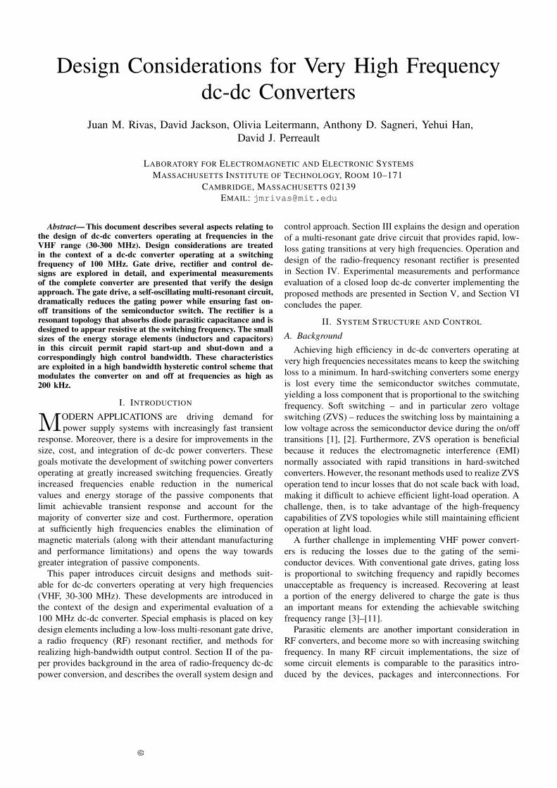
B. Converter System Structure
This paper describes a design approach that can meet all the
above requirements. A block diagram of a system realizing
this approach is shown in Fig. 1, consisting of a radio-
frequency resonant inverter, a transformation stage, and a
resonant rectifier, along with an appropriate control system.
Inverter T ra ns f o rm a ti o n S ta g e
R ec ti f i er
RLV i n
Control System
Fig. 1. A block diagram illustrating the structure of a high frequency dc-dcconverter.
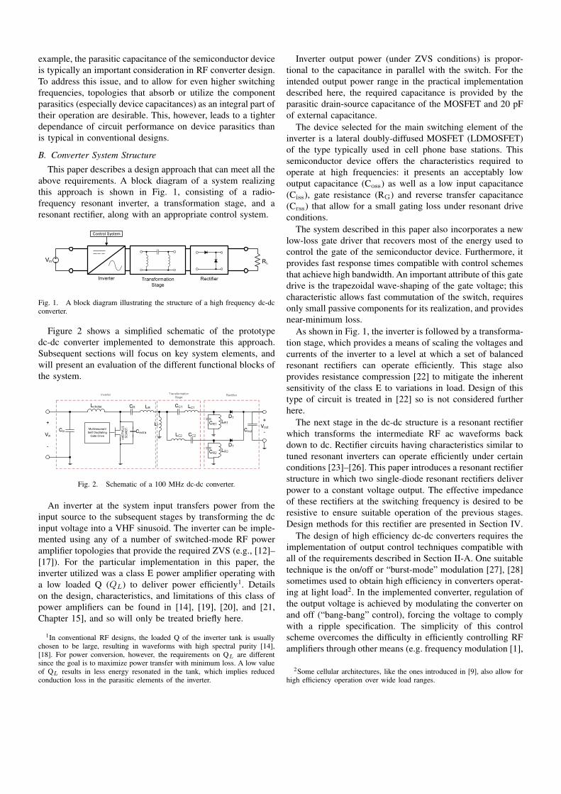
Figure 2 shows a simplified schematic of the prototype
dc-dc converter implemented to demonstrate this approach.
Subsequent sections will focus on key system elements, and
will present an evaluation of the different functional blocks of
the system.
LDMOS
373ALSR1
Lchoke
L1C i n
+
Vi n
-
+Vou t-Cex t r a
LRCR
CC2
CC1
LC2
LC1
CR1 LR1
CR2 LR2
D1
D1
Cou t
Rectifier
M u l tires o n a n tS el f O s cil l a tin gG a te D riv e
T ra n s fo r m a tio nS ta g eI n v erter
Fig. 2. Schematic of a 100 MHz dc-dc converter.
An inverter at the system input transfers power from the
input source to the subsequent stages by transforming the dc
input voltage into a VHF sinusoid. The inverter can be imple-
mented using any of a number of switched-mode RF power
amplifier topologies that provide the required ZVS (e.g., [12]–
[17]). For the particular implementation in this paper, the
inverter utilized was a class E power amplifier operating with
a low loaded Q (QL) to deliver power efficiently1. Details
on the design, characteristics, and limitations of this class of
power amplifiers can be found in [14], [19], [20], and [21,
Chapter 15], and so will only be treated briefly here.
1In conventional RF designs, the loaded Q of the inverter tank is usuallychosen to be large, resulting in waveforms with high spectral purity [14],[18]. For power conversion, however, the requirements on QL are differentsince the goal is to maximize power transfer with minimum loss. A low valueof QL results in less energy resonated in the tank, which implies reducedconduction loss in the parasitic elements of the inverter.
Inverter output power (under ZVS conditions) is propor-
tional to the capacitance in parallel with the switch. For the
intended output power range in the practical implementation
described here, the required capacitance is provided by the
parasitic drain-source capacitance of the MOSFET and 20 pF
of external capacitance.
The device selected for the main switching element of the
inverter is a lateral doubly-diffused MOSFET (LDMOSFET)
of the type typically used in cell phone base stations. This
semiconductor device offers the characteristics required to
operate at high frequencies: it presents an acceptably low
output capacitance (Coss) as well as a low input capacitance
(Ciss), gate resistance (RG) and reverse transfer capacitance
(Crss) that allow for a small gating loss under resonant drive
conditions.
The system described in this paper also incorporates a new
low-loss gate driver that recovers most of the energy used to
control the gate of the semiconductor device. Furthermore, it
provides fast response times compatible with control schemes
that achieve high bandwidth. An important attribute of this gate
drive is the trapezoidal wave-shaping of the gate voltage; this
characteristic allows fast commutation of the switch, requires
only small passive components for its realization, and provides
near-minimum loss.
As shown in Fig. 1, the inverter is followed by a transforma-
tion stage, which provides a means of scaling the voltages and
currents of the inverter to a level at which a set of balanced
resonant rectifiers can operate efficiently. This stage also
provides resistance compression [22] to mitigate the inherent
sensitivity of the class E to variations in load. Design of this
type of circuit is treated in [22] so is not considered further
here.
The next stage in the dc-dc structure is a resonant rectifier
which transforms the intermediate RF ac waveforms back
down to dc. Rectifier circuits having characteristics similar to
tuned resonant inverters can operate efficiently under certain
conditions [23]–[26]. This paper introduces a resonant rectifier
structure in which two single-diode resonant rectifiers deliver
power to a constant voltage output. The effective impedance
of these rectifiers at the switching frequency is desired to be
resistive to ensure suitable operation of the previous stages.
Design methods for this rectifier are presented in Section IV.
The design of high efficiency dc-dc converters requires the
implementation of output control techniques compatible with
all of the requirements described in Section II-A. One suitable
technique is the on/off or “burst-mode” modulation [27], [28]
sometimes used to obtain high efficiency in converters operat-
ing at light load2. In the implemented converter, regulation of
the output voltage is achieved by modulating the converter on
and off (“bang-bang” control), forcing the voltage to comply
with a ripple specification. The simplicity of this control
scheme overcomes the difficulty in efficiently controlling RF
amplifiers through other means (e.g. frequency modulation [1],
2Some cellular architectures, like the ones introduced in [9], also allow forhigh efficiency operation over wide load ranges.
- 2288 -
[8], [29], [30]). The converter system developed here is
regulated with a hysteretic controller that maintains the output
voltage within a 100 mV hysteresis band through on/off or
bang-bang control of the converter. Section V will evaluate
the performance of a 10 W dc-dc converter switching at a
frequency of 100 MHz with closed-loop voltage control.
III. SELF-OSCILLATING MULTI-RESONANT GATE DRIVE
As discussed in the previous section, reducing gating loss
is essential to operating at very high switching frequencies.
Conventional hard-switched gate drives dissipate all of the
energy delivered to the gate from the gate drive supply each
cycle. This results in a frequency dependent gate drive loss:
Pgate = Ciss · V 2gate · fs (1)
To achieve very high frequency operation while maintaining
acceptable gating loss, a resonant energy recovery gate drive
is necessary. Switch transitions are effected by ringing charge
on and off of the gate [3]–[10]. Under these conditions, most
of the energy stored on the gate is recovered and total loss
is a fraction of what can be expected if the device were hard
gated.
One approach that has been used previously is a sinusoidal
gate drive [7]–[11]. In this approach, a resonant network is
used to ring charge on and off the gate such that the gate
voltage is sinusoidal (possibly with a dc offset). For switching
times much longer than a gate RC time constant, this can be
an effective method, providing a reduced loss of:
Pgate = 2π2· f2
s · C2iss · RG · V 2
G,ac (2)
where Ciss is the gate input capacitance, RG is the effective
series resistance of the MOSFET gate and drive circuit, and
VG,ac is the peak amplitude of the sinusoidal ac gate voltage.
While a sinusoidal resonant drive is effective in some
applications, it does have some important limitations. First,
many of the commercially-available LDMOS devices suitable
for VHF power conversion incorporate a protective diode
between the source and gate terminals, preventing the use of
gate drivers which impose negative voltage excursions on the
gate. Moreover, even when a sinusoidal gate drive can be used,
the ac drive magnitude often has to be larger than needed to
fully enhance the device in order to provide a fast gate drive
transition time, increasing overall gate loss by a square law as
in (2). The negative excursions of the gate drive voltage also
induce unnecessary gate loss.
The most efficient way to charge/discharge the gate ca-
pacitance Ciss for a specified transition time is a constant
current source [31, Appendix A]. A trapezoidal drive voltage
waveform applied at the gate of the semiconductor switch
will yield an approximately constant current on the rising and
falling edges of the gate voltage (for small gate resistance RG),
thus minimizing the power dissipated in the gate resistance.
As shown in [32], the power dissipated in RG of an MOS
transistor driven by a trapezoidal waveform is:
Pgate = C2iss · V 2
gate · RG ·
[
1
tr+
1
tf
]
· fs (3)
where Vgate is the maximum voltage of the trapezoid, Ciss is
the input capacitance of the LDMOS,and tr and tf are the
rise time and the fall time respectively of the drive waveform.
Consider driving the gate of a MRF373ALSR1 LDMOSFET
(having Ciss=114 pF and RG=0.3 Ω) at a switching frequency
fs=100 MHz with the three driving schemes described above.
Hard gating with a peak gate voltage Vgate= 10 V dissipates
1.17 W. By contrast, the power dissipated by a sinusoidal
gate drive with VG,ac=15 V (large enough to rapidly enhance
the device) is only 173.16 mW. A trapezoidal driving scheme
with tr = tf =1 ns and Vgate=10 V yields a further reduced
dissipation of only 78 mW.
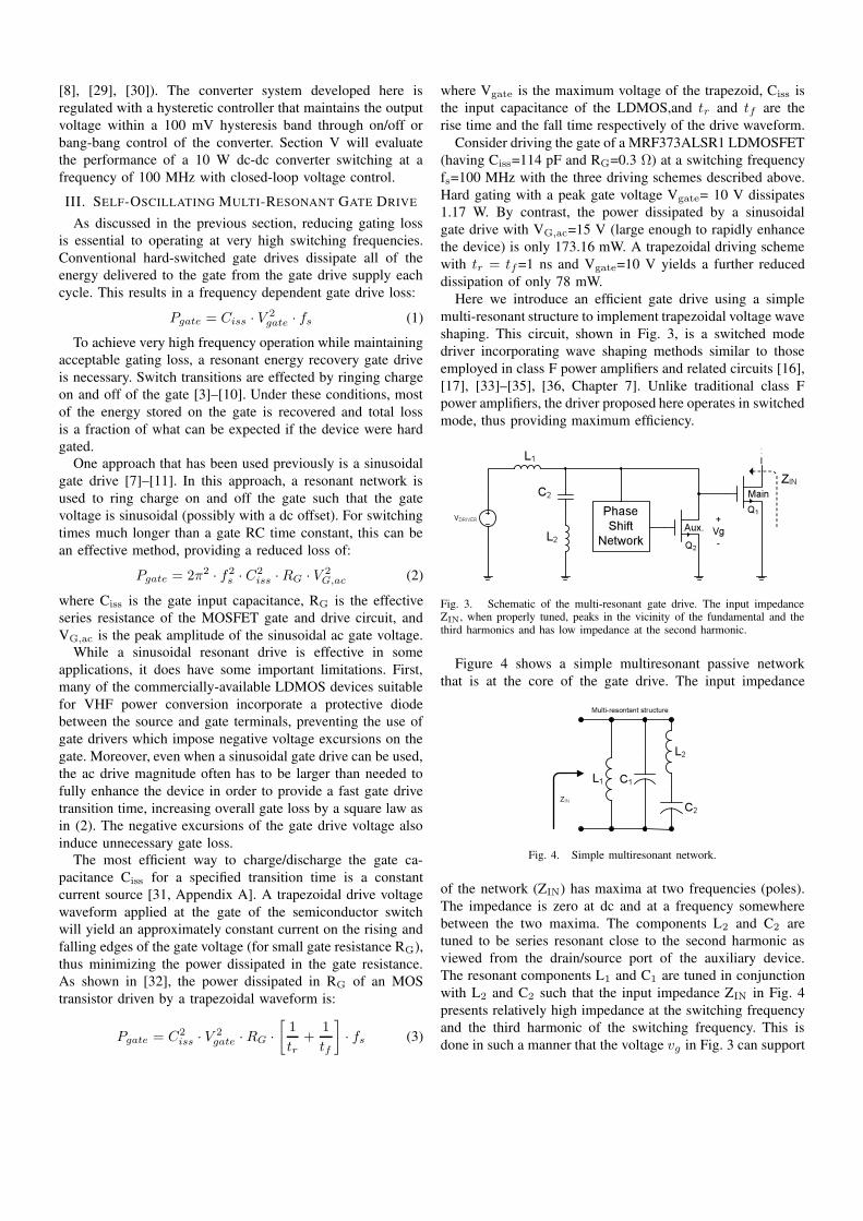
Here we introduce an efficient gate drive using a simple
multi-resonant structure to implement trapezoidal voltage wave
shaping. This circuit, shown in Fig. 3, is a switched mode
driver incorporating wave shaping methods similar to those
employed in class F power amplifiers and related circuits [16],
[17], [33]–[35], [36, Chapter 7]. Unlike traditional class F
power amplifiers, the driver proposed here operates in switched
mode, thus providing maximum efficiency.
L1
L2
C2
VDRIVERP h a s e S h i f t
N e t w o r k
ZI N
Aux.
M a i n
+V g-
Q1
Q2
Fig. 3. Schematic of the multi-resonant gate drive. The input impedanceZIN, when properly tuned, peaks in the vicinity of the fundamental and thethird harmonics and has low impedance at the second harmonic.
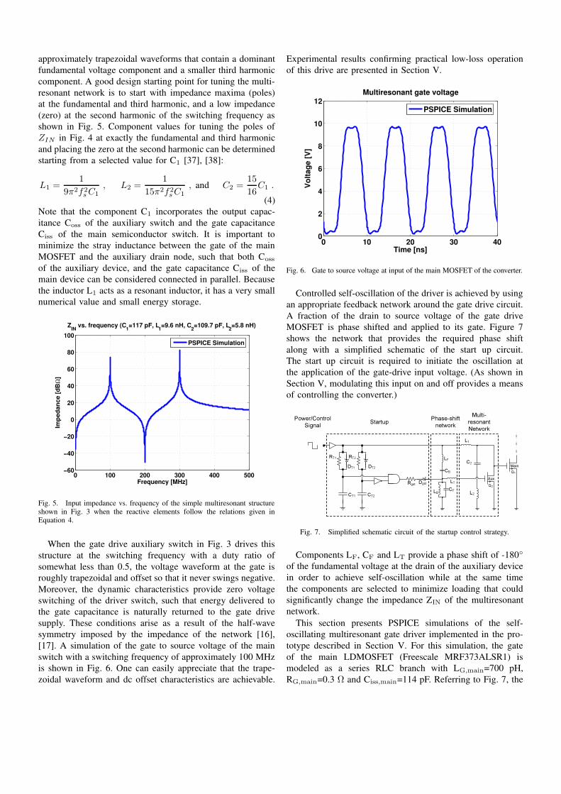
Figure 4 shows a simple multiresonant passive network
that is at the core of the gate drive. The input impedance
L1 C1
L2
C2
Multi-r e s o n ta n t s tr uc tur e
Z IN
Fig. 4. Simple multiresonant network.
of the network (ZIN) has maxima at two frequencies (poles).
The impedance is zero at dc and at a frequency somewhere
between the two maxima. The components L2 and C2 are
tuned to be series resonant close to the second harmonic as
viewed from the drain/source port of the auxiliary device.
The resonant components L1 and C1 are tuned in conjunction
with L2 and C2 such that the input impedance ZIN in Fig. 4
presents relatively high impedance at the switching frequency
and the third harmonic of the switching frequency. This is
done in such a manner that the voltage vg in Fig. 3 can support
- 2289 -
approximately trapezoidal waveforms that contain a dominant
fundamental voltage component and a smaller third harmonic
component. A good design starting point for tuning the multi-
resonant network is to start with impedance maxima (poles)
at the fundamental and third harmonic, and a low impedance
(zero) at the second harmonic of the switching frequency as
shown in Fig. 5. Component values for tuning the poles of
ZIN in Fig. 4 at exactly the fundamental and third harmonic
and placing the zero at the second harmonic can be determined
starting from a selected value for C1 [37], [38]:
L1 =1
9π2f2s C1
, L2 =1
15π2f2s C1
, and C2 =15
16C1 .
(4)
Note that the component C1 incorporates the output capac-
itance Coss of the auxiliary switch and the gate capacitance
Ciss of the main semiconductor switch. It is important to
minimize the stray inductance between the gate of the main
MOSFET and the auxiliary drain node, such that both Coss
of the auxiliary device, and the gate capacitance Ciss of the
main device can be considered connected in parallel. Because
the inductor L1 acts as a resonant inductor, it has a very small
numerical value and small energy storage.
0 100 200 300 400 500−60
−40
−20
0
20
40
60
80
100
Frequency [MHz]
Impe
danc
e [d
BΩ
]
ZIN
vs. frequency (C1=117 pF, L
1=9.6 nH, C
2=109.7 pF, L
2=5.8 nH)
PSPICE Simulation
Fig. 5. Input impedance vs. frequency of the simple multiresonant structureshown in Fig. 3 when the reactive elements follow the relations given inEquation 4.
When the gate drive auxiliary switch in Fig. 3 drives this
structure at the switching frequency with a duty ratio of
somewhat less than 0.5, the voltage waveform at the gate is
roughly trapezoidal and offset so that it never swings negative.
Moreover, the dynamic characteristics provide zero voltage
switching of the driver switch, such that energy delivered to
the gate capacitance is naturally returned to the gate drive
supply. These conditions arise as a result of the half-wave
symmetry imposed by the impedance of the network [16],
[17]. A simulation of the gate to source voltage of the main
switch with a switching frequency of approximately 100 MHz
is shown in Fig. 6. One can easily appreciate that the trape-
zoidal waveform and dc offset characteristics are achievable.
Experimental results confirming practical low-loss operation
of this drive are presented in Section V.
0 10 20 30 400
2
4
6
8
10
12Multiresonant gate voltage
Time [ns]
Vol
tage
[V]
PSPICE Simulation
Fig. 6. Gate to source voltage at input of the main MOSFET of the converter.
Controlled self-oscillation of the driver is achieved by using
an appropriate feedback network around the gate drive circuit.
A fraction of the drain to source voltage of the gate drive
MOSFET is phase shifted and applied to its gate. Figure 7
shows the network that provides the required phase shift
along with a simplified schematic of the start up circuit.
The start up circuit is required to initiate the oscillation at
the application of the gate-drive input voltage. (As shown in
Section V, modulating this input on and off provides a means
of controlling the converter.)
LT
LF
LB
L1
L2
CB
C2
CF
RT2
DT2
RT1
DT1
R g s t D g s t
StartupM ul ti -
re s o n an t N e tw o rk
P h as e -s h i f t n e tw o rk
P o w e r/C o n tro l Si g n al
Q1
Q2A u x .
M a i n
CT1 CT2
Fig. 7. Simplified schematic circuit of the startup control strategy.
Components LF, CF and LT provide a phase shift of -180
of the fundamental voltage at the drain of the auxiliary device
in order to achieve self-oscillation while at the same time
the components are selected to minimize loading that could
significantly change the impedance ZIN of the multiresonant
network.
This section presents PSPICE simulations of the self-
oscillating multiresonant gate driver implemented in the pro-
totype described in Section V. For this simulation, the gate
of the main LDMOSFET (Freescale MRF373ALSR1) is
modeled as a series RLC branch with LG,main=700 pH,
RG,main=0.3 Ω and Ciss,main=114 pF. Referring to Fig. 7, the
- 2290 -
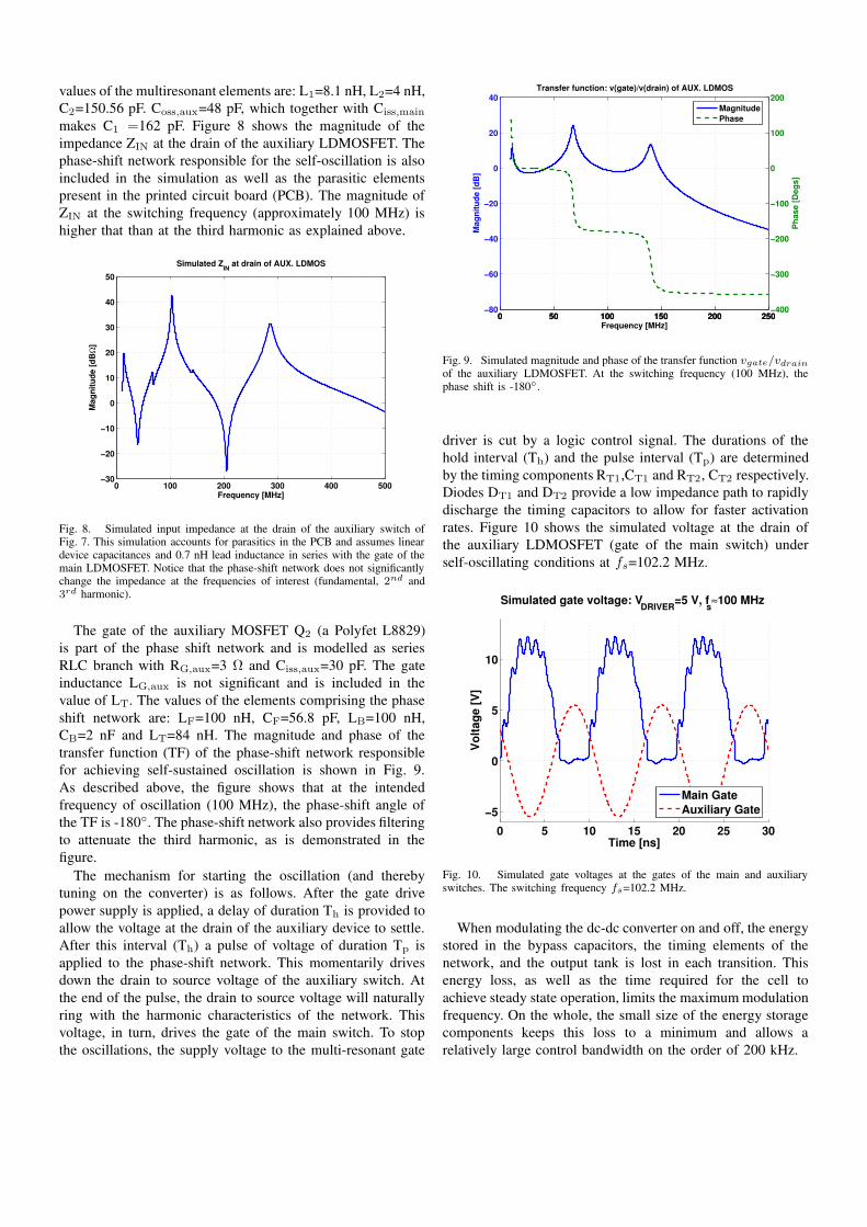
values of the multiresonant elements are: L1=8.1 nH, L2=4 nH,
C2=150.56 pF. Coss,aux=48 pF, which together with Ciss,main
makes C1 =162 pF. Figure 8 shows the magnitude of the
impedance ZIN at the drain of the auxiliary LDMOSFET. The
phase-shift network responsible for the self-oscillation is also
included in the simulation as well as the parasitic elements
present in the printed circuit board (PCB). The magnitude of
ZIN at the switching frequency (approximately 100 MHz) is
higher that than at the third harmonic as explained above.
0 100 200 300 400 500−30
−20
−10
0
10
20
30
40
50
Simulated ZIN
at drain of AUX. LDMOS
Frequency [MHz]
Mag
nitu
de [d
BΩ
]
Fig. 8. Simulated input impedance at the drain of the auxiliary switch ofFig. 7. This simulation accounts for parasitics in the PCB and assumes lineardevice capacitances and 0.7 nH lead inductance in series with the gate of themain LDMOSFET. Notice that the phase-shift network does not significantlychange the impedance at the frequencies of interest (fundamental, 2nd and3rd harmonic).
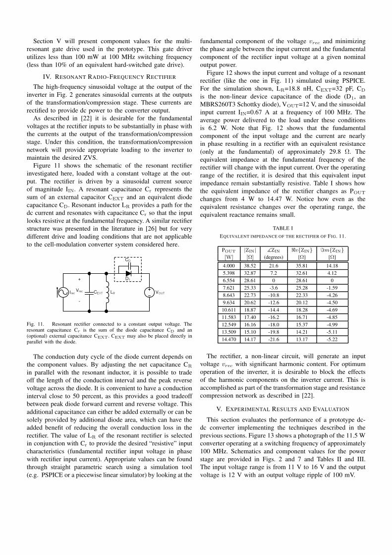
The gate of the auxiliary MOSFET Q2 (a Polyfet L8829)
is part of the phase shift network and is modelled as series
RLC branch with RG,aux=3 Ω and Ciss,aux=30 pF. The gate
inductance LG,aux is not significant and is included in the
value of LT. The values of the elements comprising the phase
shift network are: LF=100 nH, CF=56.8 pF, LB=100 nH,
CB=2 nF and LT=84 nH. The magnitude and phase of the
transfer function (TF) of the phase-shift network responsible
for achieving self-sustained oscillation is shown in Fig. 9.
As described above, the figure shows that at the intended
frequency of oscillation (100 MHz), the phase-shift angle of
the TF is -180. The phase-shift network also provides filtering
to attenuate the third harmonic, as is demonstrated in the
figure.
The mechanism for starting the oscillation (and thereby
tuning on the converter) is as follows. After the gate drive
power supply is applied, a delay of duration Th is provided to
allow the voltage at the drain of the auxiliary device to settle.
After this interval (Th) a pulse of voltage of duration Tp is
applied to the phase-shift network. This momentarily drives
down the drain to source voltage of the auxiliary switch. At
the end of the pulse, the drain to source voltage will naturally
ring with the harmonic characteristics of the network. This
voltage, in turn, drives the gate of the main switch. To stop
the oscillations, the supply voltage to the multi-resonant gate
0 50 100 150 200 250−80
−60
−40
−20
0
20
40
Frequency [MHz]
Transfer function: v(gate)/v(drain) of AUX. LDMOS
Mag
nitu
de [d
B]
0 50 100 150 200 250−400
−300
−200
−100
0
100
200
Pha
se [D
egs]
MagnitudePhase
Fig. 9. Simulated magnitude and phase of the transfer function vgate/vdrain
of the auxiliary LDMOSFET. At the switching frequency (100 MHz), thephase shift is -180.
driver is cut by a logic control signal. The durations of the
hold interval (Th) and the pulse interval (Tp) are determined
by the timing components RT1,CT1 and RT2, CT2 respectively.
Diodes DT1 and DT2 provide a low impedance path to rapidly
discharge the timing capacitors to allow for faster activation
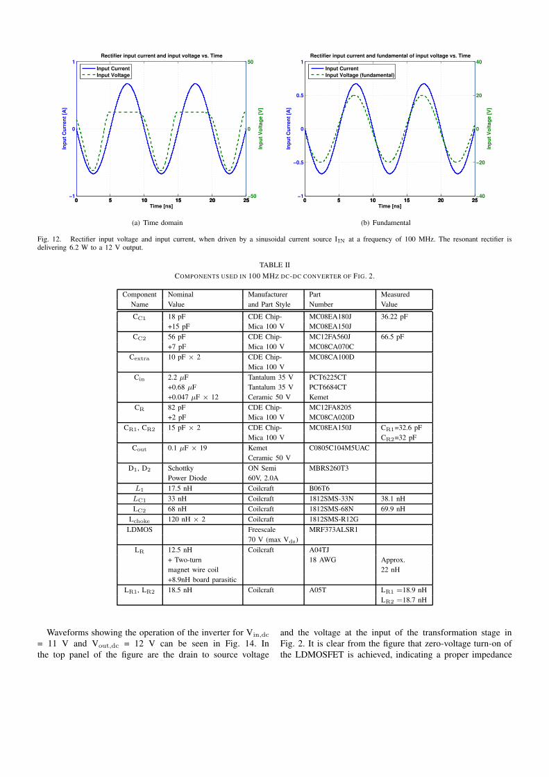
rates. Figure 10 shows the simulated voltage at the drain of
the auxiliary LDMOSFET (gate of the main switch) under
self-oscillating conditions at fs=102.2 MHz.
0 5 10 15 20 25 30
−5
0
5
10
Simulated gate voltage: VDRIVER
=5 V, fs≈100 MHz
Time [ns]
Vol
tage
[V]
Main GateAuxiliary Gate
Fig. 10. Simulated gate voltages at the gates of the main and auxiliaryswitches. The switching frequency fs=102.2 MHz.
When modulating the dc-dc converter on and off, the energy
stored in the bypass capacitors, the timing elements of the
network, and the output tank is lost in each transition. This
energy loss, as well as the time required for the cell to
achieve steady state operation, limits the maximum modulation
frequency. On the whole, the small size of the energy storage
components keeps this loss to a minimum and allows a
relatively large control bandwidth on the order of 200 kHz.
- 2291 -
Section V will present component values for the multi-
resonant gate drive used in the prototype. This gate driver
utilizes less than 100 mW at 100 MHz switching frequency
(less than 10% of an equivalent hard-switched gate drive).
IV. RESONANT RADIO-FREQUENCY RECTIFIER
The high-frequency sinusoidal voltage at the output of the
inverter in Fig. 2 generates sinusoidal currents at the outputs
of the transformation/compression stage. These currents are
rectified to provide dc power to the converter output.
As described in [22] it is desirable for the fundamental
voltages at the rectifier inputs to be substantially in phase with
the currents at the output of the transformation/compression
stage. Under this condition, the transformation/compression
network will provide appropriate loading to the inverter to
maintain the desired ZVS.
Figure 11 shows the schematic of the resonant rectifier
investigated here, loaded with a constant voltage at the out-
put. The rectifier is driven by a sinusoidal current source
of magnitude IIN. A resonant capacitance Cr represents the
sum of an external capacitor CEXT and an equivalent diode
capacitance CD. Resonant inductor LR provides a path for the
dc current and resonates with capacitance Cr so that the input
looks resistive at the fundamental frequency. A similar rectifier
structure was presented in the literature in [26] but for very
different drive and loading conditions that are not applicable
to the cell-modulation converter system considered here.
VOUTLR
D1
CD
I r e c
+
V r e c
-
CE X T
Fig. 11. Resonant rectifier connected to a constant output voltage. Theresonant capacitance Cr is the sum of the diode capacitance CD and an(optional) external capacitance CEXT. CEXT may also be placed directly inparallel with the diode.
The conduction duty cycle of the diode current depends on
the component values. By adjusting the net capacitance CR
in parallel with the resonant inductor, it is possible to trade
off the length of the conduction interval and the peak reverse
voltage across the diode. It is convenient to have a conduction
interval close to 50 percent, as this provides a good tradeoff
between peak diode forward current and reverse voltage. This
additional capacitance can either be added externally or can be
solely provided by additional diode area, which can have the
added benefit of reducing the overall conduction loss in the
rectifier. The value of LR of the resonant rectifier is selected
in conjunction with Cr to provide the desired “resistive” input
characteristics (fundamental rectifier input voltage in phase
with rectifier input current). Appropriate values can be found
through straight parametric search using a simulation tool
(e.g. PSPICE or a piecewise linear simulator) by looking at the
fundamental component of the voltage vrec and minimizing
the phase angle between the input current and the fundamental
component of the rectifier input voltage at a given nominal
output power.
Figure 12 shows the input current and voltage of a resonant
rectifier (like the one in Fig. 11) simulated using PSPICE.
For the simulation shown, LR=18.8 nH, CEXT=32 pF, CD
is the non-linear device capacitance of the diode (D1, an
MBRS260T3 Schottky diode), VOUT=12 V, and the sinusoidal
input current IIN=0.67 A at a frequency of 100 MHz. The
average power delivered to the load under these conditions
is 6.2 W. Note that Fig. 12 shows that the fundamental
component of the input voltage and the current are nearly
in phase resulting in a rectifier with an equivalent resistance
(only at the fundamental) of approximately 29.8 Ω. The
equivalent impedance at the fundamental frequency of the
rectifier will change with the input current. Over the operating
range of the rectifier, it is desired that this equivalent input
impedance remain substantially resistive. Table I shows how
the equivalent impedance of the rectifier changes as POUT
changes from 4 W to 14.47 W. Notice how even as the
equivalent resistance changes over the operating range, the
equivalent reactance remains small.
TABLE I
EQUIVALENT IMPEDANCE OF THE RECTIFIER OF FIG. 11.
POUT |ZIN| ]ZIN <eZIN =mZIN
[W] [Ω] (degrees) [Ω] [Ω]
4.000 38.52 21.6 35.81 14.18
5.398 32.87 7.2 32.61 4.12
6.554 28.61 0 28.61 0
7.621 25.33 -3.6 25.28 -1.59
8.643 22.73 -10.8 22.33 -4.26
9.634 20.62 -12.6 20.12 -4.50
10.611 18.87 -14.4 18.28 -4.69
11.583 17.40 -16.2 16.71 -4.85
12.549 16.16 -18.0 15.37 -4.99
13.509 15.10 -19.8 14.21 -5.11
14.470 14.17 -21.6 13.17 -5.22
The rectifier, a non-linear circuit, will generate an input
voltage vrec with significant harmonic content. For optimum
operation of the inverter, it is desirable to block the effects
of the harmonic components on the inverter current. This is
accomplished as part of the transformation stage and resistance
compression network as described in [22].
V. EXPERIMENTAL RESULTS AND EVALUATION
This section evaluates the performance of a prototype dc-
dc converter implementing the techniques described in the
previous sections. Figure 13 shows a photograph of the 11.5 W
converter operating at a switching frequency of approximately
100 MHz. Schematics and component values for the power
stage are provided in Figs. 2 and 7 and Tables II and III.
The input voltage range is from 11 V to 16 V and the output
voltage is 12 V with an output voltage ripple of 100 mV.
- 2292 -
0 5 10 15 20 25−1
0
1Rectifier input current and input voltage vs. Time
Time [ns]
Inpu
t Cur
rent
[A]
0 5 10 15 20 25−50
0
50
Inpu
t Vol
tage
[V]
Input CurrentInput Voltage
(a) Time domain
0 5 10 15 20 25−1
−0.5
0
0.5
1Rectifier input current and fundamental of input voltage vs. Time
Time [ns]
Inpu
t Cur
rent
[A]
0 5 10 15 20 25−40
−20
0
20
40
Inpu
t Vol
tage
[V]
Input CurrentInput Voltage (fundamental)
(b) Fundamental
Fig. 12. Rectifier input voltage and input current, when driven by a sinusoidal current source IIN at a frequency of 100 MHz. The resonant rectifier isdelivering 6.2 W to a 12 V output.
TABLE II
COMPONENTS USED IN 100 MHZ DC-DC CONVERTER OF FIG. 2.
Component Nominal Manufacturer Part Measured
Name Value and Part Style Number Value
CC1 18 pF CDE Chip- MC08EA180J 36.22 pF
+15 pF Mica 100 V MC08EA150J
CC2 56 pF CDE Chip- MC12FA560J 66.5 pF
+7 pF Mica 100 V MC08CA070C
Cextra 10 pF × 2 CDE Chip- MC08CA100D
Mica 100 V
Cin 2.2 µF Tantalum 35 V PCT6225CT
+0.68 µF Tantalum 35 V PCT6684CT
+0.047 µF × 12 Ceramic 50 V Kemet
CR 82 pF CDE Chip- MC12FA8205
+2 pF Mica 100 V MC08CA020D
CR1, CR2 15 pF × 2 CDE Chip- MC08EA150J CR1=32.6 pF
Mica 100 V CR2=32 pF
Cout 0.1 µF × 19 Kemet C0805C104M5UAC
Ceramic 50 V
D1, D2 Schottky ON Semi MBRS260T3
Power Diode 60V, 2.0A
L1 17.5 nH Coilcraft B06T6
LC1 33 nH Coilcraft 1812SMS-33N 38.1 nH
LC2 68 nH Coilcraft 1812SMS-68N 69.9 nH
Lchoke 120 nH × 2 Coilcraft 1812SMS-R12G
LDMOS Freescale MRF373ALSR1
70 V (max Vds)
LR 12.5 nH Coilcraft A04TJ
+ Two-turn 18 AWG Approx.
magnet wire coil 22 nH
+8.9nH board parasitic
LR1, LR2 18.5 nH Coilcraft A05T LR1 =18.9 nH
LR2 =18.7 nH
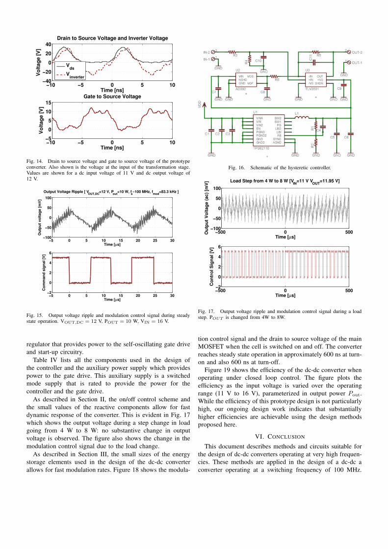
Waveforms showing the operation of the inverter for Vin,dc
= 11 V and Vout,dc = 12 V can be seen in Fig. 14. In
the top panel of the figure are the drain to source voltage
and the voltage at the input of the transformation stage in
Fig. 2. It is clear from the figure that zero-voltage turn-on of
the LDMOSFET is achieved, indicating a proper impedance
- 2293 -
TABLE III
COMPONENTS USED IN THE SELF-OSCILLATING MULTI-RESONANT GATE DRIVE OF FIG. 7.
Component Nominal Manufacturer Part Measured
Name Value and Part Style Number Value
L1 PCB trace 8.1 nH
C1 48 pF Coss,aux 162 pF
+114 pF Ciss,main
L2 PCB trace 4 nH
C2 100 pF CDE Chip- MC12FA101J 150.56 pF
+47 pF Mica 100 V MC12FA470J
+4 pF MC08CA040D
LF 100 nH Coilcraft 1812SMS-R10 L 100 nH
CB 2 nF Ceramic 50 V Kemet 2 nF
CF 47 pF CDE Chip- MC12FA470J 56.8 pF
+5 pF Mica 100 V MC08CA050D
+3 pF MC08CA030D
LB 100 nH Coilcraft 1812SMS-R10 L 100 nH
LT 82 nH Coilcraft 1812SMS-82N L 84 nH
RT1 1 kΩ Rohm, 0805, 1/8 W, 1 % MCR10EZHF1001 1 kΩ
CT1 100 pF Kemet, 0805, 50 V C0805C101J1GAC 325 pF
+220 pF Kemet, 0805, 50 V C0805C221J5GACTU
DT1 Diodes Inc. BAS70-7
RT2 2.43 kΩ Rohm, 0805, 1/8 W, 1 % MCR10EZHF2431 2.43 kΩ
CT2 100 pF Kemet, 0805, 50 V C0805C101J1GAC 325 pF
+220 pF Kemet, 0805, 50 V C0805C221J5GACTU
DT2 Diodes Inc. BAS70-7
Rgst 100 Ω‖100 Ω Rohm, 0805, 1/8 W, 1 % MCR10EZHF1000 50 Ω
Dgst Diodes Inc. BAS70-7
IC1 National LLP-6 LM5115
IC2 National LLP-6 LM5115
Auxiliary LDMOS Polyfet SO-8 L88219
Fig. 13. Power stage of the prototype 100 MHz dc-dc power converter.
match. Shown at the bottom of the same figure is the gate
to source voltage driving the semiconductor switch. The total
power dissipated by the gate driver, including the startup
circuitry, was measured to be less than 100 mW, which is more
than an order of magnitude less than the power that would be
dissipated had the switch been driven with conventional hard-
switched gating (and lower than the 300 mW dissipation of
an earlier implementation of this gate drive [22]).
The output voltage ripple is shown in Fig. 15 when
VOUT,DC = 12 V, POUT = 10 W. Under these conditions,
the controller modulates the converter on and off at 83.3 kHz
to provide the average power required to regulate the output.
The control signal modulating the converter system on and
off is shown in the lower trace of Fig. 15. This control
signal commands the converter either to operate or to remain
inactive depending on the conditions of the output voltage. The
resulting output ripple is approximately 100 mV peak to peak,
independent of load. In the figure, the 100 MHz switching
ripple (observed as the “hash” when the output voltage is
rising) is under-sampled in the time scale shown. While the
modulating frequency is on the order of 100 kHz, most of
the the energy storage components in the converter are sized
based on the 100 MHz switching frequency. Only the input and
output capacitors are sized based on the modulation frequency.
The modulation frequency is determined by the loading condi-
tions, the allowed hysteresis band around the nominal output
voltage, and the size of the output filter capacitor. In the
implemented design, the maximum modulation frequency was
in excess of 200 kHz. Figure 16 shows the schematic for
the hysteretic modulation controller and the switched-mode
- 2294 -
−10 −5 0 5 10−40
−20
0
20
40Drain to Source Voltage and Inverter Voltage
Time [ns]
Vol
tage
[V]
Vds
Vinverter
−10 −5 0 5 10−5
0
5
10
15Gate to Source Voltage
Time [ns]
Vol
tage
[V]
Fig. 14. Drain to source voltage and gate to source voltage of the prototypeconverter. Also shown is the voltage at the input of the transformation stage.Values are shown for a dc input voltage of 11 V and dc output voltage of12 V.
−5 0 5 10 15 20 25 30−100
−50
0
50
100
Time [µs]
Out
put v
olta
ge [m
V]
Output Voltage Ripple [ VOUT,DC
=12 V, Pout
=10 W, fs≈100 MHz, f
mod=83.3 kHz ]
−5 0 5 10 15 20 25 30−2
0
2
4
6
Time [µs]
Com
man
d si
gnal
[V]
Fig. 15. Output voltage ripple and modulation control signal during steadystate operation. VOUT,DC = 12 V, POUT = 10 W, VIN = 16 V.
regulator that provides power to the self-oscillating gate drive
and start-up circuitry.
Table IV lists all the components used in the design of
the controller and the auxiliary power supply which provides
power to the gate drive. This auxiliary supply is a switched
mode supply that is rated to provide the power for the
controller and the gate drive.
As described in Section II, the on/off control scheme and
the small values of the reactive components allow for fast
dynamic response of the converter. This is evident in Fig. 17
which shows the output voltage during a step change in load
going from 4 W to 8 W: no substantive change in output
voltage is observed. The figure also shows the change in the
modulation control signal due to the load change.
As described in Section III, the small sizes of the energy
storage elements used in the design of the dc-dc converter
allows for fast modulation rates. Figure 18 shows the modula-
Fig. 16. Schematic of the hysteretic controller.
−500 0 500−100
−50
0
50
100
Time [µs]
Out
put V
olta
ge (a
c) [m
V] Load Step from 4 W to 8 W [V
IN=11 V V
OUT=11.95 V]
−500 0 500−2
0
2
4
6
Time [µs]
Con
trol
Sig
nal [
V]
Fig. 17. Output voltage ripple and modulation control signal during a loadstep. POUT is changed from 4W to 8W.
tion control signal and the drain to source voltage of the main
MOSFET when the cell is switched on and off. The converter
reaches steady state operation in approximately 600 ns at turn-
on and also 600 ns at turn-off.
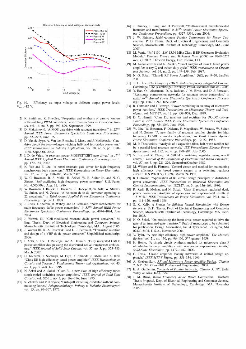
Figure 19 shows the efficiency of the dc-dc converter when
operating under closed loop control. The figure plots the
efficiency as the input voltage is varied over the operating
range (11 V to 16 V), parameterized in output power Pout.
While the efficiency of this prototype design is not particularly
high, our ongoing design work indicates that substantially
higher efficiencies are achievable using the design methods
proposed here.
VI. CONCLUSION
This document describes methods and circuits suitable for
the design of dc-dc converters operating at very high frequen-
cies. These methods are applied in the design of a dc-dc a
converter operating at a switching frequency of 100 MHz.
- 2295 -
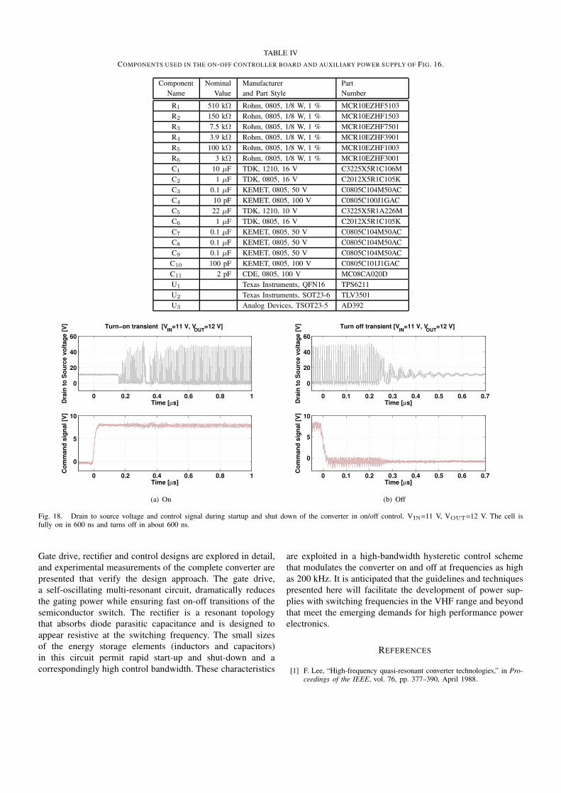
TABLE IV
COMPONENTS USED IN THE ON-OFF CONTROLLER BOARD AND AUXILIARY POWER SUPPLY OF FIG. 16.
Component Nominal Manufacturer Part
Name Value and Part Style Number
R1 510 kΩ Rohm, 0805, 1/8 W, 1 % MCR10EZHF5103
R2 150 kΩ Rohm, 0805, 1/8 W, 1 % MCR10EZHF1503
R3 7.5 kΩ Rohm, 0805, 1/8 W, 1 % MCR10EZHF7501
R4 3.9 kΩ Rohm, 0805, 1/8 W, 1 % MCR10EZHF3901
R5 100 kΩ Rohm, 0805, 1/8 W, 1 % MCR10EZHF1003
R6 3 kΩ Rohm, 0805, 1/8 W, 1 % MCR10EZHF3001
C1 10 µF TDK, 1210, 16 V C3225X5R1C106M
C2 1 µF TDK, 0805, 16 V C2012X5R1C105K
C3 0.1 µF KEMET, 0805, 50 V C0805C104M50AC
C4 10 pF KEMET, 0805, 100 V C0805C100J1GAC
C5 22 µF TDK, 1210, 10 V C3225X5R1A226M
C6 1 µF TDK, 0805, 16 V C2012X5R1C105K
C7 0.1 µF KEMET, 0805, 50 V C0805C104M50AC
C8 0.1 µF KEMET, 0805, 50 V C0805C104M50AC
C9 0.1 µF KEMET, 0805, 50 V C0805C104M50AC
C10 100 pF KEMET, 0805, 100 V C0805C101J1GAC
C11 2 pF CDE, 0805, 100 V MC08CA020D
U1 Texas Instruments, QFN16 TPS6211
U2 Texas Instruments, SOT23-6 TLV3501
U3 Analog Devices, TSOT23-5 AD392
0 0.2 0.4 0.6 0.8 1
0
20
40
60
Time [µs]Dra
in to
Sou
rce
volta
ge [V
] Turn−on transient [VIN
=11 V, VOUT
=12 V]
0 0.2 0.4 0.6 0.8 1
0
5
10
Time [µs]
Com
man
d si
gnal
[V]
(a) On
0 0.1 0.2 0.3 0.4 0.5 0.6 0.7
0
20
40
60
Time [µs]Dra
in to
Sou
rce
volta
ge [V
] Turn off transient [VIN
=11 V, VOUT
=12 V]
0 0.1 0.2 0.3 0.4 0.5 0.6 0.7
0
5
10
Time [µs]
Com
man
d si
gnal
[V]
(b) Off
Fig. 18. Drain to source voltage and control signal during startup and shut down of the converter in on/off control. VIN=11 V, VOUT=12 V. The cell isfully on in 600 ns and turns off in about 600 ns.
Gate drive, rectifier and control designs are explored in detail,
and experimental measurements of the complete converter are
presented that verify the design approach. The gate drive,
a self-oscillating multi-resonant circuit, dramatically reduces
the gating power while ensuring fast on-off transitions of the
semiconductor switch. The rectifier is a resonant topology
that absorbs diode parasitic capacitance and is designed to
appear resistive at the switching frequency. The small sizes
of the energy storage elements (inductors and capacitors)
in this circuit permit rapid start-up and shut-down and a
correspondingly high control bandwidth. These characteristics
are exploited in a high-bandwidth hysteretic control scheme
that modulates the converter on and off at frequencies as high
as 200 kHz. It is anticipated that the guidelines and techniques
presented here will facilitate the development of power sup-
plies with switching frequencies in the VHF range and beyond
that meet the emerging demands for high performance power
electronics.
REFERENCES
[1] F. Lee, “High-frequency quasi-resonant converter technologies,” in Pro-
ceedings of the IEEE, vol. 76, pp. 377–390, April 1988.
- 2296 -
11 12 13 14 15 160.64
0.66
0.68
0.7
0.72
0.74
0.76
Input Voltage [V]
Con
verte
r Effi
cien
cyConverter Efficiency vs Input Voltage at Various Loads
Pout=11.5 WPout=10 WPout=8 WPout=6 WPout= 4 W
Fig. 19. Efficiency vs. input voltage at different output power levels.Vout=12 V.
[2] K. Smith and K. Smedley, “Properties and synthesis of passive losslesssoft-switching PWM converters,” IEEE Transactions on Power Electron-
ics, vol. 14, no. 5, pp. 890–899, September 1999.[3] D. Maksimovic, “A MOS gate drive with resonant transitions,” in 22nd
Annual IEEE Power Electronics Specialists Conference Proceedings,pp. 527–532, June 1991.
[4] D. Van de Sype, A. Van den Bossche, J. Maes, and J. Melkebeek, “Gate-drive circuit for zero-voltage-switching half- and full-bridge converters,”IEEE Transactions on Industry Applications, vol. 38, no. 5, pp. 1380–1388, Sept./Oct. 2002.
[5] I. D. de Vries, “A resonant power MOSFET/IGBT gate driver,” in 17th
Annual IEEE Applied Power Electronics Conference Proceedings, vol. 1,pp. 179–185, 2002.
[6] K. Yao and F. Lee, “A novel resonant gate driver for high frequencysynchronous buck converters,” IEEE Transactions on Power Electronics,vol. 17, no. 2, pp. 180–186, March 2002.
[7] W. C. Bowman, R. S. Malik, H. Seidel, W. B. Suiter Jr., and N. G.Ziesse, “Self-oscillating high frequency power converter.” U.S. PatentNo. 4,605,999., Aug. 12, 1986.
[8] W. Bowman, J. Balicki, F. Dickens, R. Honeycutt, W. Nitz, W. Strauss,W. Suiter, and N. Zeisse, “A resonant dc-to-dc converter operating at22 megahertz,” in Third Annual Applied Power Electronics Conference
Proceedings, pp. 3–11, 1988.[9] J. Rivas, J. Shafran, R. Wahby, and D. Perreault, “New architectures for
radio-frequency dc/dc power conversion,” in 35th Annual IEEE PowerElectronics Specialists Conference Proceedings, pp. 4074–4084, June2004.
[10] J. Warren, III, “Cell-modulated resonant dc/dc power converter,” M.Eng. Thesis, Dept. of Electrical Engineering and Computer Science,Massachusetts Institute of Technology, Cambridge, MA., August 2005.
[11] J. Warren III, K. A. Rosowski, and D. J. Perreault, “Transistor selectionand design of a VHF dc-dc power converter.” Unpublished manuscript,2006.
[12] I. Aoki, S. Kee, D. Rutledge, and A. Hajimiri, “Fully integrated CMOSpower amplifier design using the distributed active transformer architec-ture,” IEEE Journal of Solid-State Circuits, vol. 37, no. 3, pp. 373–383,March 2002.
[13] H. Koizumi, T. Suetsugu, M. Fujii, K. Shinoda, S. More, and K. Iked,“Class DE high-efficiency tuned power amplifier,” IEEE Transactions onCircuits and Systems I: Fundamental Theory and Applications, vol. 43,no. 1, pp. 51–60, Jan. 1996.
[14] N. Sokal and A. Sokal, “Class E—a new class of high-efficiency tunedsingle-ended switching power amplifiers,” IEEE Journal of Solid-StateCircuits, vol. SC-10, no. 3, pp. 168–176, June 1975.
[15] S. Zhukov and V. Kozyrev, “Push-pull switching oscillator without com-mutating losses,” Poluprovodnikovye Pribory v. Tekhnike Elektrosvyazi,vol. 15, pp. 95–107, 1975.
[16] J. Phinney, J. Lang, and D. Perreault, “Multi-resonant microfabricatedinductors and transformers,” in 35th Annual Power Electronics Special-
ists Conference Proceedings, pp. 4527–4536, June 2004.
[17] J. W. Phinney, Multi-resonant Passive Components for Power Con-version. Ph.D. Thesis, Dept. of Electrical Engineering and ComputerScience, Massachusetts Institute of Technology, Cambridge, MA., June2005.
[18] M. Vania, “Prf-1150 1kW 13.56 MHz Class E RF Generator EvaluationModule,” Directed Energy, Inc. Technical Note, (DOC no. 9200-0255
Rev. 1), 2002. Directed Energy, Fort Collins, CO.
[19] M. Kazimierczuk and K. Puczko, “Exact analysis of class E tuned poweramplifier at any Q and switch duty cycle,” IEEE transactions on Circuits
and Systems, vol. 34, no. 2, pp. 149–159, Feb. 1987.
[20] N. O. Sokal, “Class-E RF Power Amplifiers,” QEX, pp. 9–20, Jan/Feb2001.
[21] T. H. Lee, The Design of CMOS Radio-Frequency Integrated Circuits.Cambridge, UK: (Cambridge University Press), second edition ed., 2004.
[22] Y. Han, O. Leitermann, D. A. Jackson, J. M. Rivas, and D. J. Perreault,“Resistance compression networks for resonant power conversion,” inIEEE 36th Annual Power Electronics Specialists Conference Proceed-ings, pp. 1282–1292, June 2005.
[23] R. Gutmann and J. Borrego, “Power combining in an array of microwavepower rectifiers,” IEEE Transactions on Microwave Theory and Tech-niques, vol. MTT-27, no. 12, pp. 958–968, Dec. 1979.
[24] D. C. Hamill, “Class DE inverters and rectifiers for DC-DC conver-sion,” in 27th Annual IEEE Power Electronics Specialists Conference
Proceedings, pp. 854–860, June 1996.
[25] W. Nitz, W. Bowman, F. Dickens, F. Magalhaes, W. Strauss, W. Suiter,and N. Zeisse, “A new family of resonant rectifier circuits for highfrequency DC-DC converter applications,” in Third Annual AppliedPower Electronics Conference Proceedings, pp. 12–22, 1988.
[26] M. P. Theodoridis, “Analysis of a capacitive-filter, half-wave rectifier fedby a parallel-load resonant network,” IEE Proceedings: Electric PowerApplications, vol. 152, no. 4, pp. 878–884, July 2005.
[27] Y. Lee and Y. Cheng, “A 580 kHz switching regulator using on-offcontrol,” Journal of the Institution of Electronic and Radio Engineers,vol. 57, no. 5, pp. 221–226, September/October 1987.
[28] M. Wilcox and R. Flatness, “Control circuit and method for maintaininghigh efficiency over broad current ranges in a switching regulatorcircuit.” U.S Patent 5,731,694, March 24 1998.
[29] R. Gutmann, “Application of RF circuit design principles to distributedpower converters,” IEEE Transactions on Industrial Electronics and
Control Instrumentation, vol. IEC127, no. 3, pp. 156–164, 1980.
[30] R. Redl, B. Molnar, and N. Sokal, “Class E resonant regulated dc/dcpower converters: Analysis of operations and experimental results at1.5 MHz,” IEEE Transactions on Power Electronics, vol. PE-1, no. 2,pp. 111–120, April 1986.
[31] S. K. Kelly, A System for Efficient Neural Stimulation with Energy
Recovery. Ph.D. Thesis, Dept. of Electrical Engineering and ComputerScience, Massachusetts Institute of Technology, Cambridge, MA, Octo-ber 2003.
[32] N. O. Sokal, “On predicting the input-drive power required to drive thegate of an insulated-gate transistor.” Draft of manuscript to be submittedfor publication, Design Automation, Inc. 4 Tyler Road Lexington, MA02420-2404, U.S.A., November 2004.
[33] V. Tyler, “A new high-efficiency high-power amplifier,” The Marconi
Review, vol. 21, no. 130, pp. 96–109, 3rd quarter 1958.
[34] K. Honjo, “A simple circuit synthesis method for microwave class-Fultra-high-efficiency amplifiers with reactance-compensation circuits,”Solid-State Electronics, pp. 1477–1482, 2000.
[35] C. Trask, “Class-f amplifier loading networks: A unified design ap-proach,” IEEE MTT-S Digest, pp. 351–354, 1999.
[36] A. Grebennikov, RF and Microwave Power Amplifer Design, Chapter
7. NY: (Mc Graw-Hill Professional Engineering), 2005.
[37] E. A. Guillemin, Synthesis of Passive Networks, Chapter 3. NY: (JohnWiley & sons, Inc.), 1957.
[38] J. M. Rivas, Radio Frequency dc-dc Power Conversion. DoctoralThesis Proposal, Dept. of Electrical Engineering and Computer Science,Massachusetts Institute of Technology, Cambridge, MA, November2005.
- 2297 -