Embed Size (px)
Citation preview
Welcome to the 2016 Joint NSLS-ll & CFN Users’ Meeting!
We are very pleased that you have joined us for the 2016 Joint National Synchrotron Light Source ll (NSLS-ll) and Center for Functional Nanomaterials (CFN) Users’ Meeting. This year, the theme of our meeting is “Illuminating the Future” as we focus on the exciting new prospects of NSLS-ll, and the continuing excellence of CFN. The program includes invited talks, workshops, a poster session, and exhibits highlighting new technology and instrumentation - all offering opportunities to learn about the latest developments in synchrotron and nanoscience experimentation that can impact your own research.The Plenary session will be held on Tuesday. The key note speaker will be Chi-Chang Kao, Director of the SLAC National Accelerator Laboratory, along with invited speakers, Arthur Nozik, Senior Research Fellow Emeritus of the National Renewable Energy Laboratory (NREL) and Department of Chemistry at the University of Colorado, Boulder, and Henry Chapman, Division Director, Coherent Imaging Team, Center for Free-Electron Laser Science, DESY and Professor of Physics at the University of Hamburg. The session will also include presentations from the Lead Beamline Scientists for the five newest NSLS-ll operating beamlines, with updates on planned capabilities and early science commissioning results. This year we have the special privilege of hearing from Cherry Murray about activities at the U.S. Department of Energy, as well as updates on activities at BNL from Doon Gibbs; at the NSLS-ll from John Hill; and at the CFN from Chuck Black.Also, this year we will be hosting nine scientific workshops, covering a broad range of topics. The NSLS-ll and CFN Users’ Executive Committees and the Organizing Committee acknowledge the outstanding work of our workshop organizers: Andi Barbour, Fernando Camino, Alessandra Colli, Mircea Cotlet, Dean DeLongchamp, Michael Dudley, Lars Ehm, Andrei Fluerasu, Martin Fuchs, Gabriele Giacomini, Mingzhao Liu, Lee Makowski, Claudio Mazzoli, Jack Mershon, Chang-Yong Nam, Ben Ocko, John Parise, Balaji Raghothamachar, Richard Reeder, Abdul Rumaiz, Jurek Sadowski, Martin Schoonen, Davood Shahrjerdi, Mikala Shremshock, D. Peter Siddons, Donald Weidner, Lutz Wiegart, Stuart Wilkins, Kevin Yager, Lin Yang, Shinjae Yoo, Dmitri Zakharov and Yugang Zhang. We also thank all of the workshop speakers, the poster presenters, and the poster judges for their time and effort.Finally, both UECs thank the amazing folks in the NSLS-ll and CFN User Administration Offices and the BNL staff, all of whom do the hard work every year to provide us with a great Users’ Meeting.
We hope that you will enjoy all of the scientific and social events of the 2016 meeting!Organizing Committee MembersDonald Weidner, Meeting and Program Co-Chair, Stony Brook UniversityStanislaus Wong , Meeting and Program Co-Chair and Poster Chair, Stony Brook UniversityBruce Ravel, Workshop Coordinator, NISTGretchen Cisco, NSLS-ll User Administrator, Meeting Coordinator and Sponsor Chair, Brookhaven National LaboratoryNancye Wright, Meeting Coordinator and Vendor Chair, Brookhaven National LaboratoryGrace Webster, CFN User Administrator, Brookhaven National Laboratory

Welcome ..........................................................................................................................................1NSLS-ll UEC Community Service Award .........................................................................................42016 Julian David Baumert Ph.D. Thesis Award .............................................................................5Student Scholarship Recipents .......................................................................................................6Main Meeting Agenda ......................................................................................................................18Workshop 1 Two-Dimensional van der Waals Semiconductors for Energy Conversion Applications ............ 24Workshop 2 Meeting the Challenges of Big Data Sets ........................................................................................ 27Workshop 3 Operando Structural Characterization of Polymer Processing ...................................................31Workshop 4 SEM Stereo Imaging and 3D Reconstruction for Metrology: A Total Hands-on Workshop ........ 36Workshop 5 Renewable Energies: Where Applied and Basic Sciences Meet ................................................. 37Workshop 6 The Earth Laboratory: Experimental and Computational Tools and Infrastructure for Cross-cutting Earth Sciences ................................................................................................41Workshop 7 Scanning X-ray Microdiffraction ....................................................................................................... 45Workshop 8 New Detectors for New Light Sources .......................................................................................50Workshop 9 Probing Dynamics in Soft and Hard Condensed Matter with Coherent X-rays ..........................55BNL Site Map ..................................................................................................................................60Exhibitor and Sponsor Information Location of Equipment and Instrumentation Exhibitors in Berkner Hall .....................................61 Exhibitors at Workshops located at Chemistry Department, Bldg. 555 ......................................62 Exhibitors at Workshops located at CFN, Bldg. 735 and Exhibitor Presentations .....................62 Sponsors ....................................................................................................................................63 Exhibitor Advertisements and Presentations ..............................................................................64 List of Equipment and Instrumentation Exhibitors ......................................................................65Accommodations .............................................................................................................................79Offsite Transportation ......................................................................................................................80Onsite Transportation ......................................................................................................................81Nominees for the 2016-18 Users’ Executive Committee .................................................................83
ContentsMay 23-25, 2016

UEC Community Service Award Recipient
John Trunk
User operation has begun in earnest at the NSLS-II, but wait, the NSLS-II isn’t finished yet… This is the predicament of most of the staff. Users are coming to run on some beamlines while IRR’s need to be prepared for others. This year we honor John Trunk for his skills in navigating this challenging landscape. He has demonstrated a dedication to excellence, with a strong commitment to users. John, a mechanical engineer, was part of the team that brought XPD to life and now divides his time supporting XPD users, and bringing the ISR beamline to readiness. He joined BNL in 1982 and had worked with the Biology department on a number of their NSLS beamlines and several others before transferring to the NSLS-II in 2014.Users of XPD express considerable thanks for John’s support for their science. As one user reported, “John should receive this award for three reasons: 1) Admiration of his peers – this is one of the key indicators of a person’s value to his colleagues and community, 2) Dedication to users – this allows users to perform quality science with total support when they need it most, and 3) Commitment to the safety at NSLS-II – this allows science to continue to be performed and benefits the NSLS-II community as a whole.”
John Trunk

Awards
2016 Julian David Baumert Ph.D. Thesis Award
Kip E. Guja
Kip E. Guja, a postdoctoral researcher and Medical Scientist Training Program (MSTP) Fellow at Stony Brook University, is the 2016 recipient of the Julian Baumert Ph.D. Thesis Award. Jiang was selected for his thesis research on “The Determination of Three-dimension Protein Structure and Shape Information via an X-ray Crystallography and Small-angle X-ray Scattering in Soluton Experiments at the NSLS." The Baumert Award is given to a researcher who has recently conducted a thesis project that included measurements at the National Synchrotron Light Source (NSLS) or National Synchrotron Light Source II (NSLS-II). It was established in memory of Julian David Baumert, a young Brookhaven physicist who was working on x-ray studies of soft-matter interfaces at NSLS before he died in June 2006. Dr. Guja’s doctoral thesis work was based on the determination of 3D protein structure and shape information via X-raycrystallography and small-angle X-ray scattering in solution
experiments at NSLS. His work comprised three subprojects: mitochondrial gene expression, characterization of novel therapeutic targets in Mycobacterium tuberculosis, and characterization of a novel anti-cancer drug target involved in sphingomyelin metabolism and cancer metastasis.Dr. Guja graduated with a Ph.D. in Biochemistey and Structural Biology from Stony Brook University and is currently pursuing his Doctor of Medicine under the guidance of Miquel Garcia-Diaz, an Associate Professor in the Department of Pharmacological Sciences at Stony Brook University.In his letter of recommendation, Garcia-Diaz stated, “Kip’s performance in my group was nothing short of stellar. He quickly became an accomplished structural biologist, frequently using X-ray crystallography and SAXS. Moreover, unlike most students, Kip became intimately familiar with both techniques.”Garcia-Diaz also said, “Kip’s thesis represents an important contribution to our understanding of several aspects of mitochondrial gene expression.”Dr. Guja served as an instructor for two NSLS programs: RapiData and X9 SAXS Workbench. He conducted research at beamlines X9, X25, and X29. He reports that the novel structure of nSMase2 was solved via single-wavelength anomalous dispersion methods at X25 using selenium substituted protein. Also using beamline X25, his group solved the first crystal structure of nSMase2 at 1.85-A resolution and gain important insights into its regulation by lipids. The group was also able to determine the first structures of a heterotetrameric MaoC-like enoyl-CoA hydratase, a novel drug target known as ChsH1-ChsH2, which is encoded by two adjacent genes from the igr operon of Mtb. Genes from the igr operon, such as those encoding ChsH1-ChsH2 are known to play an essential role in Mtb cholesterol metabolism, which is required for pathogenesis during the latent stage of Mtb infection.Dr. Guja writes in his summary statement that the beamlines at NSLS were crucial to his work. When it came to solving the crystal structure of the novel anti-cancer drug target, he said, “This breakthrough was only made possible by the high dynamic range and minimal background signal attainable with the pixel-array detector at X25.” He added that the identification of 3D structures of mycobacterium tuberculosis was uniquely enabled by the characteristics of that beamline, and that the high throughput capability at beamline X29 and the SAXS data collected at X9 allowed for a successful reconstruction of the mitochondrial transcription iniation complex. The Baumert Award will be presented on May 24 during the 2016 NSLS-II and CFN Users’ Meeting. Kip will receive a $600 honorarium and travel arrangements to the meeting, where he will give a 15-minute presentation on his thesis work. His name will be engraved on a plaque in NSLS-II.
Kip E. Guja

The Users’ Executive Committee (UEC) offers a student scholarship program that provides opportunites for students to attend the meeting. The following abstracts are presented by the recipients of this year’s scholarship award. For more information about the student scholarship program: http://usersmeeting.ps.bnl.gov/page.aspx?year=2016&id=scholarships
Argon Blocks the Way
Nusnin Akter a, JianQiang Zhong b, Mengen Wang a, John Kestell b, Ira Waluyo c, Dario Stacchiola b,d, Deyu Lu b, Taejin Kim a,e, J. Anibal Boscoboinik* a,b
a Department of Materials Science and Engineering, Stony Brook University, Stony Brook, NY, 11794, USA
b Center for Functional Nanomaterials, Brookhaven National Laboratory, Upton, NY 11973, USA
c Photon Science Division, National Synchrotron Light Source II, Brookhaven National Laboratory, Upton, NY 11973, USA
d Chemistry Department, Brookhaven National Laboratory, Upton, NY 11973, USAe Department of Chemical and Molecular Engineering, Stony Brook University, Stony Brook, NY,
11794, USA
e-mail: [email protected]; [email protected].
CO at elevated pressures penetrates readily through two-dimensional zeolite model systems consisting of a nanoporous crystalline ultra-thin (0.5 nm) aluminosilicate films to adsorb on a Ru(0001) surface. In this work we carry out infrared reflection absorption spectroscopy (IRRAS) experiments to show that, for the case of an all-Si 2D-zeolite model, trapping Argon atoms within the nanopores blocks the passage of CO molecules. This then prevents the adsorption of CO on the Ru(0001) surface. The trapping of Ar atoms on the 2D-zeolite model was also demonstrated by ambient pressure XPS at the CSX-2 beamline of NSLS-II.
ACKNOWLEDGMENT: Research carried out in part at the CSX-2 beamline of the National Synchrotron Light Source II, Chemistry Department and Center for Functional Nanomaterials, Brookhaven National Laboratory, which is supported by the U.S. Department of Energy, Office of Basic Energy Sciences, under Contract No. DE-SC0012704. We gratefully acknowledge the financial support for this study from SBU/BNL 2015 SEED grant (N.A.) and the Department of Materials Science & Engineering at Stony Brook University through start-up research funding(T.K.). J.Z. is supported by BNL LDRD Project No. 15-010. We gratefully acknowledge the help from C. Mazzoli, A. Barbour, S. Wilkins, Kazimierz G., Larry F., Steve B. and Andrew M. at NSLS-II.

Awards
Chain Conformation near the Substrate Interface in Nanoparticle Stabilized
Polymer Thin Films
Deborah A. Barkleya, Mani Senb, Naisheng Jiangb, Maya K. Endohb, Jonathan G. Rudicka,
Tadanori Kogaa, b, Yugang Zhangc, Lutz Wiegartc, Andrei Fluerasuc, Oleg Gangd,
Guangcui Yuane, Sushil K. Satijae, Alamgir Karimf
aDepartment of Chemistry, Stony Brook University, Stony Brook, NY 11794-3400bDepartment of Materials Science and Engineering, Stony Brook University, Stony Brook, NY
11794-2275cNSLS-II, Brookhaven National Lab, Upton, NY 11973
dCenter for Functional Nanomaterials, Brookhaven National Lab, Upton, NY 11973eCenter for Neutron Research, National Institute of Standards and Technology, Gaithersburg,
MD 20899fCollege of Polymer Science and Polymer Engineering, University of Akron, Akron Ohio, 44325-0301
Addition of a diverse array of inorganic nanoparticles to ultrathin polymer films is vital to achieve the necessary attributes for the next-generation polymer thin film technology including sensors, energy conversion devices, and coatings. At the same time, nanoparticles have been used to stabilize ultrathin polymer films against dewetting: they often migrate to the film-substrate interface and form a “diffused immobile interfacial layer”, which serves to screen the polymer-substrate interaction, imparts pining to the contact line, and suppress dewetting. An un-solved question is how the conformations of the polymer chains in the immobile layer are affect-ed by the nanoparticles and the relationship with the improvement of film stability. To address the question, dodecane thiol-functionalized gold nanoparticles (2.8 nm in diameter) and polysty-rene (PS, Mw = 30 kDa and 50 kDa) were used as a rational model. We found that the Au nano-particles induce complete dewetting suppression of 20 nm-thick PS/Au thin films on cleaned Si substrates at 0.25% (volume of the particle/volume of the polymer). To investigate the interfacial structures at the polymer-solid interface, we rinsed the annealed PS/Au thin films with toluene and characterized the residual interfacial layers by using a suite of surface sensitive experimental techniques including X-ray reflectivity, grazing incidence small angle X-ray scattering, X-ray photon correlation spectroscopy (at NSLS/NSLS-II), atomic force microscopy, X-ray photoelec-tron spectroscopy, and scanning electron microscopy (at CFN). The results indicate that when nanoparticles are added, the conformation of the polymer chains becomes elongated and the ad-sorbed chains can act as “connector molecules” to stabilize the thin film.
Acknowledgement: We acknowledge the financial support from NSF Grant (CMMI -1332499).
Triple Evaporation of Alkali Antimonides
Zihao Dinga, John Sinshiemera, Mengjia Gaoweib, Erik Mullera and John Smedleyb
aStony Brook University, Stony Brook, NY, bBrookhaven National Laboratory, Upton, NY,
Corresponding Email: [email protected]
Bialkali antimonide photocathode CsK2Sb is an excellent candidate as an electron source in awide range of applications, because of its high quantum efficiency, low emittance, fast response and good lifetime. In recent years, synchrotron X-ray methods have been used to study the growth mechanism of K2CsSb photocathodes. It has been found that surface roughness of this photocathode grown by traditional recipe is about 25 nm over a 100 nm period, which was measured by a UHV-AFM. This magnitude of surface roughness is not favorable in the photocathode application in the next generation light sources. It is therefore necessary and demanding to explore a novel growth method, such as triple evaporation of K, Cs and Sb, to produce a photocathode with high quantum efficiency and low surface roughness.
In this study, triple evaporation growth of K, Cs and Sb is used to fabricate K2CsSb photocathode on the substrate of single-crystalline Si (100) and MgO (001). In-situ synchrotron X-ray fluorescence (XRF), X-ray diffraction (XRD) and X-ray reflectivity (XRR) are applied during triple evaporation growth to characterize the thin film quality. Surface roughness of the photocathodes are found to be around 2-4 nm. QE at the wavelength of 532 nm are measured to be around 2%. Correct stoichiometry of K2CsSb has been confirmed by real time XRF analysis. XRD analysis has shown that Cs2KSb crystals are formed more preferably than CsK2Sb under this growth condition.

Awards
Influence of Cadmium Overpressure on the the Crystalline Quality of Cadmium Zinc Telluride Single Crystals
Ouloide Yannick [email protected]
Cadmium Zinc Telluride (CZT) single crystals are the material of choice for the room temperature detection of γ-rays and hard x-rays in security, medical and space applications. Obtaining high quality single crystal is a challenge in the growth of CZT crystals, and the high density of structural imperfections limits the detection power of CZT-based detectors and their energy resolution. Further a critical requirement for CdZnTe detector applications is high electrical resistivity to reduce the bulk leakage current. By growing CdZnTe under controlled Cd over-pressures, high resistivity has been reproducibly obtained. However, it is also necessary to obtain a thorough understanding of this growth modification on the structural quality of the crystals grown. In this study, the influence of Cadmium (Cd) overpressure on the growth of CZT single crystals by vertical directional solidification (Bridgman technique) method is evaluated. To that end, boules with different Cd over-pressures were grown. Axial and transverse slices cut from the boules and polished were investigated using a combination of synchrotron white beam x-ray topography (SWBXT), Infrared spectroscopy and double axis x-ray diffraction. Preliminary SWBXT results reveals the presence of twining and a uniform distribution of a network of subgrain boundaries and dislocations. Infrared mapping revealed a high density of Te inclusions, which decorated twin boundaries and aligned along subgrain boundaries and dislocations. The Te inclusions have circular and triangular shapes, and their size is between 10 to 60µm. These results will shed light on the influence of Cd overpressure on the structural perfection of CZT crystals.

In situ Probing of the Active Site Geometry of Ultrathin Nanowires for the Oxygen Reduction Reaction
Haiqing Liu, Stony Brook University
To create truly effective electrocatalysts for the cathodic reaction governing proton exchange membrane fuel cells (PEMFC), namely the oxygen reduction reaction (ORR), necessitates an accurate and detailed structural understanding of these electrocatalysts, especially at the nanoscale, and to precisely correlate that structure with demonstrable performance enhancement. To address this key issue, we have combined and interwoven theoretical calculations with experimental, spectroscopic observations in order to acquire useful structural insights into the active site geometry with implications for designing optimized nanoscale electrocatalysts with rationally predicted properties. Specifically, we have probed ultrathin (~2 nm) core-shell Pt~Pd9Au nanowires, which has been previously shown to be excellent candidates for ORR in terms of both activity and long-term stability, from the complementary perspectives of both DFT calculations and X-ray Absorption Spectroscopy (XAS). The combination and correlation of data from both experimental and theoretical studies has revealed for the first time that the catalytically active structure of our ternary nanowires can actually be ascribed to PtAu~Pd possessing a PtAu binary shell and a pure inner Pd core. Moreover, we have plausibly attributed the resulting structure to a specific synthesis step, namely the Cu underpotential deposition (UPD) followed by galvanic replacement with Pt. Hence, the fundamental insights gained into the performance of our ultrathin nanowires from our demonstrated approach will likely guide future directed efforts aimed at broadly improving upon the durability and stability of nanoscale electrocatalysts in general.
Awards
0D-2D Semiconducting Hybrids with Enhanced Absorption and Charge Mobility
Prahlad K. Routh1,2, H. Zang2, Y. Huang2, Peter Sutter2, Chang-Yong Nam1 and Mircea Cotlet2
1Materials Science & Engineering Department, Stony Brook University, Stony Brook, NY2Center for Functional Nanomaterials, Brookhaven National Laboratory, Upton, NY
[email protected], phone 631-344-7596, cell 631-745-0985
Emerging 2-D semiconductors, especially layered metal dichalcogenides (LMDs) such as MoS2,WS2 and WSe2 have shown great potential applications in photocatalysis, photon detectors and energy harvesting. These materials show band structure dependence on the number of layers and band-gap inversion at monolayer with intense visible photoluminescence, making them interesting candidates for photosensing applications. However, their low dimensionality makesphoton absorption poor. In this study we present a straightforward method to increase photon absorption in such LMDs. We show that doping of single and few-layer of tin disulphide (SnS2), with colloidal CdSe/ZnS quantum dots (QDs) results in 0D-2D hybrids with large photon absorption cross-section and high charge mobility. Using time resolved single nanocrystals photoluminescence microscopy and monitoring the blinking dynamics of QDs alone and part of the LMD, we were able to unveil the interaction between the two nanoscale components as non-radiative energy transfer and to find that the rate of this process increases with the increase in the number of SnS2 layers [1]. We also found that such 0D-2D hybrids, when incorporated into field effect transistor devices, outperformed the LMD only devices by 500% in the photocurrent response and displayed substantially increased spectral responsivity [2].
References:
1. Zang, H.*, Routh, P. K.*, Huang, Y.*, Chen, J. S., Sutter, E., Sutter, P., & Cotlet, M., Nonradiative Energy Transfer from Individual CdSe/ZnS Quantum Dots to Single-Layer and Few-Layer Tin Disulfide. ACS Nano, 2016. (*Equally contributing author)
2. Huang, Y., Zang, H., Chen, J. S., Sutter, E. A., Sutter, P. W., Nam, C. Y., & Cotlet, M. Hybrid quantum dot-tin disulfide field-effect transistors with improved photocurrent and spectral responsivity. AppliedPhysics Letters, 2016, 108, 123502.

Self-assembly of Block Copolymers at the Polymer-solid InterfaceMani Sen1, Naisheng Jiang1, Bhoje Gowd1, 2, Maya K. Endoh1, Tadanori Koga1, 3
1Department of Materials Science and Engineering, Stony Brook University, Stony Brook, New York 11794-2275
2Materials Science and Technology Division, CSIR-National Institute for Interdisciplinary Science and Technology, Trivandrum-695 019, Kerala, India
3Chemical and Molecular Engineering Program, Stony Brook University, Stony Brook, NY 11794-2275
Block copolymer thin films offer a simple and effective route to fabricate highly ordered periodic microdomain structures. The fundamental, yet unsolved question is whether these highly orient-ed microdomain structures persist even near an impenetrable solid wall. We here report adsorbed structures of polystyrene-block-poly (4-vinylpyridine) (PS-block-P4VP, Mw=41,000, weight fraction of PS=0.81) formed on planar silicon substrates. Perpendicularly aligned cylindrical mi-crodomains were created by a solvent vapor annealing process as a model and the strongly bound polymer layer onto the substrate surface was derived by solvent leaching with chloroform, agood solvent for the polymers, and thereafter characterized by using atomic force microscopy, scanning electron microscopy (at CFN), grazing incidence small angle X-ray scattering, and x-ray reflectivity at NSLS. The results showed that both PS and P4VP chains lie flat on the sub-strate, forming a heterogeneous two-dimensional structure without long-range order. Moreover, a spin-coated PS-block-P4VP thin film annealed under vacuum at 190 °C (>Tg of both blocks, but below the order-disorder temperature) showed a similar microscopic heterogeneous structure on the substrate, indicating the generality of the interfacial self-assembling block copolymer struc-tures.
Acknowledgement: We acknowledge the financial support from NSF Grant (CMMI -1332499).

Awards
First Principles Study of Core Level Binding Energy Shift and Noble Gas Adsorption in Two-dimensional Zeolites
Mengan Wang Materials Science and Engineering Department, Stony Brook University
Jianqiang Zhong, Jorge Anibal Boscoboinik, and Deyu Lu Center for Functional Nanomaterials, Brookhaven National Laboratory
Zeolites are important industrial catalysts with porous three-dimensional structures. The catalytically active sites are located inside the pores, thus rendering them inaccessible for surface science measurements. A two-dimensional (2D) zeolite model system has be synthesized, which consists of (alumino)silicate bilayer films weakly bound to Ru(0001) surface. The 2D zeolite allows a detailed characterization of the atomic structure of the active site and interrogation of the model system during the catalytic reaction. We carried out density functional theory (DFT) calculations to understand the mechanism of the experimental observed core level binding energy shift of silica films during reversible oxidation and reduction of Ru(0001) surface. In near ambient pressure core level XPS spectra, O 1s binding energy in silica films red-shifts during oxidation of Ru(0001), while O 1s on Ru(0001) remains unchanged. DFT calculations based on van der Waals density functionals reveal that, during the chemisorption of oxygen atoms on Ru(0001), charge transfer leads to surface and interfacial dipole moments that modify the vacuum potential. Consequently, this electrostatic effect shifts the work function of Ru(0001) and causes the O 1s core level bind energy shift as coverage of the chemisorbed oxygen atoms increases. Ar atoms adsorbed in the silica film may block the active site, which requires a careful study. Experimental studies found that Ar atoms can be trapped either inside the hexagonal prism nano-cages of the silica films or at the interface between the silica films and Ru(0001). DFT calculations were carried out to determine the preferred Ar adsorption sites, the corresponding adsorption energies, and adsorption/desorption energy barriers.
This research used resources of the Center for Functional Nanomaterials, which is a U.S. DOE Office of Science Facility, at Brookhaven National Laboratory under Contract No. DE-SC0012704.

Assessment of Factors Controlling the X-ray Penetration Depth in Studies of 4H-SiC using Monochromatic Synchrotron X-ray Topography in Grazing
Incidence Geometry
Synchrotron X-ray Topography has been shown to be a vital tool for the nondestructive characterization of defects in 4H-SiC crystals. Techniques utilizing reflection geometry are particularly useful for discerning defects at different depths below the crystal surface. For example, in studying defects in SiC pin diode structures, which typically comprise a buffer layer homoepitaxially grown on a substrate, with the drift layer grown on top of the buffer layer, it is important to be able to discriminate the depth at which particular defect configurations reside. This is particularly important for the characterization of defects resulting from relaxation processes such as interfacial dislocations and half loop arrays. A discrepancy has been found between the penetration depth calculated theoretically by considering a dislocation under kinematical diffraction conditions and the value measured experimentally. Moreover, the penetration depths measured from deflected threading screw dislocations and the basal plane dislocations are found to be different. Accurate discernment of the depth of a defect requires precise measurement of the effective penetration depth of the X-ray beam in the diffraction geometry in question. This paper provides an assessment of the factors controlling that penetration depth in grazing incidence geometries. There are generally two approaches adopted depending of the level of perfection of the crystal. In deformed regions (such as around dislocation cores) the penetration depth is simply determined by photoelectric absorption. In perfect regions it is determined by extinction. We will present a comparison between measured penetration depths in various diffraction geometries with those calculated using these two approaches and develop an optimized model to explain our observations.
Awards
Effects of Thermal Annealing on Structural and Optical Properties of ZnO-Polymer Hybrid Thin Film Generated by Infiltration Synthesis
Xinyi Ye1 and Chang-Yong Nam1,2
1Department of Materials Science and Engineering, Stony Brook University, Stony Brook, New York 11794
2Center for Functional Nanomaterials, Brookhaven National Laboratory, Upton, New York 11973
Infiltration synthesis is a process derived from atomic layer deposition, where the sequential infiltration of vapor-phase material precursors into polymer matrix enables the generation of organic-inorganic hybrids with enhanced properties, such as mechanical strength, etch resistance, triboelectric performance, and photoluminescence. Most of the demonstrated hybrids are however based on the infiltration of aluminum oxide that has relatively limited intrinsic functionalities compared with other electro-active counterparts, such as zinc oxide (ZnO), a wide band-gap semiconductor having favorable features including photo-catalytic activity, visible optical luminescence, and piezoelectricity. Infiltration synthesis of ZnO in polymers therefore has a potential for creating new type of organic-inorganic hybrids with useful multi-functional properties. In this work, we generated hybrid thin films consisting of infiltration-synthesized ZnO in SU-8, a epoxy-based negative-tone polymer photoresist, and investigated the influence of precursor infiltration and post-synthesis thermal annealing conditions on the structural and optical properties of the hybrid thin films. Specifically, the sequential vapor infiltration of diethylzinc (DEZ) and water was applied into SU-8 thin films at 85 oC, with varying precursorinfiltration protocol and the number of synthesis cycles. Cross-sectional scanning electronmicroscopy and energy dispersive x-ray spectroscopy confirmed the infiltration of ZnO in SU-8matrix. After annealing the hybrid film at 250 oC, we observed the highest photoluminescence (PL) intensity with its peak centered around 520 nm. Further increasing the annealing temperature up to 400 oC, however, decreased the PL intensity, suggesting the presence of chemical interaction between the infiltrated ZnO molecules and the polymer matrix. Fourier-transform infrared spectroscopy and ultraviolet-visible spectroscopy showed that the infiltrated ZnO mainly reacted with epoxy groups in SU-8 at the higher temperature, subsequently resulting in a red shift in the optical absorption spectrum of the hybrid film. The current study not only demonstrates the formation of visible-luminescent ZnO-infiltrated hybrid thin film but also improves the understanding of the interaction of organometallic precursor with polymer and its correlation with the infiltration synthesis protocol and thermal annealing conditions, providing the information critical for generating multi-functional inorganic-organic hybrid materials by infiltration synthesis process.

Detecting the Future: Diamond X-ray Detector
Tianyi Zhoua, Mengnan Zoua, Mengjia Gaoweib, Jen Bohonc, John Smedleyb and Erik Mullera
aStony Brook University, Stony Brook, NY, bBrookhaven National Laboratory, Upton, NY,cCase Western Reserve University, Cleveland, OH.
Corresponding Email: [email protected]
Diamond is the ultimate material for x-ray detecting due to its large bandgap (low thermal noise, Schotkky barrier), low absorption (transmission mode), radiation hardness (long lifetime) ,high carrier mobility (quick signal response) and the highest thermal conductivity (low heat build-upand expansion). Unlike traditional radiation detectors, diamond is not suffering from electronics saturation and heat dispersion problems as in silicon diodes, and it is not environmental sensitive as in ion chambers and does not require delicate electronics. We have built various transmission mode diamond detectors for beam flux, beam position and real-time imaging in NSLS, NSLS II, APS, CHESS, LANL and etc. Furthermore, thin diamond membrane (less than 10um) detector fabricated by deep RIE could be used for soft x-ray detection. Ultra-nanocrystalline diamond (UNCD) contacts are under development for even less absorption. In this poster, a detailed study of diamond detector performance is included; in addition, the preliminary results of diamond response under Compton region (over 30keV) and diamond membrane fabrication are discussed.
Awards
Diamond X-ray Detector with Ultrananocrystalline Diamond Contacts
Mengnan Zoua, Tianyi Zhoua, Mengjia Gaoweib, Ani Sumantc, Jen Bohond,John Smedleyb and Erik M. Mullera
aStony Brook University, Stony Brook, NY, bBrookhaven National Laboratory, Upton, NY,cCase Western Reserve University, Cleveland, OH., dArgonne National Laboratory, Argonne, IL
Corresponding Email: [email protected]
Due to its extraordinary properties of radiation hardness, thermal conductivity and large bandgap, diamond is an ideal material for X-ray detectors. Traditional diamond X-ray detectors arefabricated with metal contacts, such as platinum, and provide absolute flux calibration and position resolution better than 50nm. However, for many energy scanning applications the absorption lines from the metallic contacts effect the downstream experiment. Therefore, we have incorporated a conducting ultra-thin nano-crystalline diamond (UNCD) as the contact material, which shares all the benefits of diamond without the absorption lines associated with metal contacts. We will present results from several detectors fabricated with UNCD contacts where the contacts have been patterned with reactive ion etching into quadrant or single channel devices. The UNCD is grown at the Center for Nanoscale Materials at Argonne National Laboratory. The design, preparation and patterning is done at the Center for Functional Nanomaterials. The detectors were tested at BNL and CHESS and they display uniform response and full collection.

AgendaSunday, May 22, 2016
May 23-25, 2016
Starts Ends Event Location4:00 p.m. 7:00 p.m. Optional Vendor and Poster Set Up Berkner Hall
Lobby and Cafeteria
4:00 p.m. 7:00 p.m. Early Registration - Registration Office Opens Berkner Hall Lobby and Room D
AgendaMonday, May 23, 2016
Starts Ends Event Location7:00 a.m. 5:30 p.m. Registration Office Opens ~ all attendees must check in before
attending any eventBerkner Hall Lobby and Room D
7:00 a.m. 11:30 a.m. Vendor Exhibit and Poster Set Up Berkner Hall Lobby and Cafeteria
8:30 a.m. 5:15 p.m. Workshop 1: Two-Dimensional van der Waals Semiconductors for Energy Conversion Applications
CFN Bldg. 735, Large Conf. Room
8:30 a.m. 6:00 p.m. Workshop 2: Meeting the Challenges of Big Data Sets Berkner Hall, Bldg. 488, Conf. Room B
9:00 a.m. 5:30 p.m. Workshop 3: Operando Structural Characterization of Polymer Processing
Chemistry Bldg. 555, Hamilton Seminar Room
2:30 p.m. 6:00 p.m. Workshop 4: SEM Stereo Imaging and 3D Reconstruction for Metrology: A Total Hands-on Workshop
CFN Bldg. 735, Small Conf. Room B
12:30 p.m. 1:30 p.m. Lunch Break - All workshop attendees will go to Berkner Hall (included - Luncheon ticket required)
Berkner Hall, Cafeteria
1:30 p.m. 2:30 p.m. Exhibitor and Poster Session - Please note in addition to the evening reception (Monday, 5/23 at 5:30pm), there will be an Exhibitor and Poster Sessions during the lunch periods (12:30 to 2:30 pm) on both Monday and Wednesday. All lunches will be held at Berkner Hall, allowing all meeting participants to attend the sessions. Please use this time to visit the Exhibitors and Posters.
Berkner Hall Lobby and Cafe

Agendas
Welcome Reception, exhibitoR and posteR session
Monday, May 23, 2016 - 5:30 pm - 8:00 pmCome join us for an opportunity to view the exhibits and network with over 60 NSLS-ll and CFN vendors. Also, more than 50 posters, submitted by scientists, researchers, post docs and students exhibiting their research at the NSLS-ll and CFN, will be on display. The Poster Session will open Monday, May 23, at 12:30 p.m. and close Wednesday, May 25, at 2:30 p.m. It will be located in close proximity to the vendor instrumentation/equipment exhibit and refreshments.
Hot and cold hors-d’oeuvres and refreshments will be served.
Registered attendees (general and student) receive one ticket to the Welcome Reception, compliments of our sponsors and exhibitors. Additional tickets (guests and free plenary registration) may be purchased for $20.
6:00 p.m. All Workshops Conclude Workshop Locations
5:30 p.m. Registration Office Closes Berkner Hall Conf. Rm. D
5:30 p.m. 8:00 p.m. Welcome Reception, Vendor Exhibit and Poster SessionOur Welcome Reception will highlight the Vendor Exhibit and a Poster Session. Hot and cold hors-d’oeuvres will be served and refreshments. Combining these popular events makes for a very successful evening.
Berkner HallLobby and Cafeteria
5:30 p.m. 8:00 p.m. Discovery Park and BNL Quality of Life/Infrastructure Berkner Hall Lobby
NSLS-II Tours
Come see the new exciting happenings at NSLS-II! Tours will be held on Monday, Tuesday, and Wednesday. Sign up at the registration desk in Berkner Hall.

Early Morning Plenary Session Open to all, free of charge (registration is required)
(8:30 a.m. to 10:55 a.m.)Session Chair, Jean Jordan-Sweet
IBM Research Chair, NSLS-ll Users’ Executive Committee
Starts Ends Event Location8:30 a.m. 8:35 a.m. “Welcome”
Donald Weidner, Distinguished Professor, Stony Brook University
Berkner HallAuditorium
8:35 a.m. 8:55 a.m. “BNL Update” Doon Gibbs, Director, Brookhaven National Laboratory
Berkner HallAuditorium
8:55 a.m. 9:40 a.m. “Department of Energy Office of Science Update”, Cherry Murray, Director of the Department of Energy’s Office of Science, U.S. Department of Energy
Berkner HallAuditorium
9:40 a.m. 10:25 a.m. “Keynote Talk”, Chi-Chang Kao, Director, SLAC, National Accelerator Laboratory
Berkner HallAuditorium
AgendaTuesday, May 24, 2016
Starts Ends Event Location7:30 a.m. 5:00 p.m. Registration Office Opens ~ all attendees must check in before
attending any eventBerkner Hall Lobby and Room D
8:00 a.m. 5:00 p.m. Vendor Exhibit and Poster Session Berkner Hall Lobby and Cafeteria
May 23-25, 2016
Morning Break - Continental Breakfast (included) (10:25 a.m. to 10:55 a.m.)
Starts Ends Event Location10:25 a.m. 1:30 p.m. Discovery Park and BNL Quality of LIfe/Infrastructure Berkner Hall
Lobby10:25 a.m. 12:15 p.m. BNL Exhibitors Networking Session and Presentations (Open to
all BNL)Berkner Hall Lobby and Cafeteria
10:25 a.m. 10:35 a.m. Photo: NSLS-ll/CFN UEC Members, BNL and DOE Management Behind Berkner
10:35 a.m. 10:45 a.m. Photo: Users’ Meeting Planning Committee Behind Berkner

Agendas
Late Morning Plenary Session Open to all, free of charge (registration is required)
(10:55 a.m. to 12:15 p.m.)
Session Chair, Donald Weidner, Stony Brook UniversityVice Chair, NSLS-ll Users’ Executive Committee
Starts Ends Event Location10:55 a.m. 11:25 a.m. “NSLS-ll Update”, John Hill, Deputy Associate Lab Director for
Basic Energy Sciences & Photon Sciences, NSLS-ll Director, Brookhaven National Laboratory
Berkner HallAuditorium
11:25 a.m. 11:45 a.m. “Beamline Talk 1”, Klaus Attenkofer, Lead Beamline Scientist for Inner-Shell Spectroscopy (ISS) Beamline, NSLS-II, Brookhaven National Laboratory
Berkner HallAuditorium
11:45 a.m. 12:05 p.m. “Beamline Talk 2”, Lin Yang, Lead Beamline Scientist for Life Science X-ray Scattering (LiX) Beamline, NSLS-II, Brookhaven National Laboratory
Berkner HallAuditorium
12:05 p.m. 12:15 p.m. UEC Election Results Berkner HallAuditorium
Lunch Break(Luncheon Ticket Required)
(12:15 p.m. to 1:30 p.m.)
Starts Ends Event Location1:30 p.m. 5:30 p.m. BNL Exhibitors Networking Session and Presentations (Open to
BNL)Berkner Hall Lobby and Cafeteria
1:30 pm 2:00 pm “CFN Update”, Charles Black, Director, Center for Functional Nanomaterials, Brookhaven National Laboratory
Berkner Hall Auditorium
2:00 pm 2:40 pm Plenary Talk 1: “Advanced Concepts for Efficient Solar Photon Conversion to PV and Fuels Based on Nanoscience”, Arthur Nozik, Department of Chemistry, University of Colorado at Boulder/NREL
Berkner Hall Auditorium
2:45 pm 3:00 pm Poster Winners and Community Service Award Berkner Hall Auditorium
Early Afternoon Plenary Session Open to all, free of charge (registration is required)
(1:30 p.m. to 2:45 p.m.)
Session Chair, Nathlie Bouet Brookhaven National Laboratory
Chair, CFN Users Executive Committee
Starts Ends Event Location12:15 p.m. 1:30 p.m. Joint UEC lunch with DOE, Office of Basic Energy Sciences Berkner Hall
Conf. Rm. A
Afternoon Break (3:00 p.m. to 3:20 p.m.)
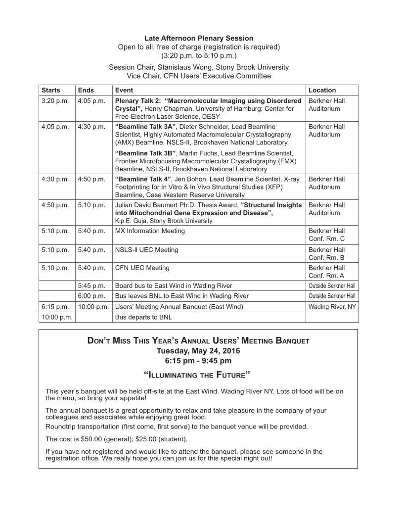
Late Afternoon Plenary Session Open to all, free of charge (registration is required)
(3:20 p.m. to 5:10 p.m.)Session Chair, Stanislaus Wong, Stony Brook University
Vice Chair, CFN Users’ Executive Committee
Starts Ends Event Location3:20 p.m. 4:05 p.m. Plenary Talk 2: “Macromolecular Imaging using Disordered
Crystal”, Henry Chapman, University of Hamburg; Center for Free-Electron Laser Science, DESY
Berkner HallAuditorium
4:05 p.m. 4:30 p.m. “Beamline Talk 3A”, Dieter Schneider, Lead Beamline Scientist, Highly Automated Macromolecular Crystallography (AMX) Beamline, NSLS-II, Brookhaven National Laboratory “Beamline Talk 3B”, Martin Fuchs, Lead Beamline Scientist, Frontier Microfocusing Macromolecular Crystallography (FMX) Beamline, NSLS-II, Brookhaven National Laboratory
Berkner HallAuditorium
4:30 p.m. 4:50 p.m. “Beamline Talk 4”, Jen Bohon, Lead Beamline Scientist, X-ray Footprinting for In Vitro & In Vivo Structural Studies (XFP) Beamline, Case Western Reserve University
Berkner HallAuditorium
4:50 p.m. 5:10 p.m. Julian David Baumert Ph.D. Thesis Award, “Structural Insights into Mitochondrial Gene Expression and Disease”, Kip E. Guja, Stony Brook University
Berkner HallAuditorium
5:10 p.m. 5:40 p.m. MX Information Meeting Berkner Hall Conf. Rm. C
5:10 p.m. 5:40 p.m. NSLS-ll UEC Meeting Berkner Hall Conf. Rm. B
5:10 p.m. 5:40 p.m. CFN UEC Meeting Berkner HallConf. Rm. A
5:45 p.m. Board bus to East Wind in Wading River Outside Berkner Hall6:00 p.m. Bus leaves BNL to East Wind in Wading River Outside Berkner Hall
6:15 p.m. 10:00 p.m. Users’ Meeting Annual Banquet (East Wind) Wading River, NY10:00 p.m. Bus departs to BNL
don’t miss this YeaR’s annual useRs’ meeting banquet Tuesday, May 24, 2016
6:15 pm - 9:45 pm
This year’s banquet will be held off-site at the East Wind, Wading River NY. Lots of food will be on the menu, so bring your appetite!
The annual banquet is a great opportunity to relax and take pleasure in the company of your colleagues and associates while enjoying great food. Roundtrip transportation (first come, first serve) to the banquet venue will be provided.
The cost is $50.00 (general); $25.00 (student).
If you have not registered and would like to attend the banquet, please see someone in the registration office. We really hope you can join us for this special night out!
“illuminating the FutuRe”

Agendas
AgendaWednesday, May 25, 2016
Starts Ends Event Location8:00 a.m. 2:30 p.m. Registration Office Opens ~ all attendees must check in before
attending any eventBerkner Hall Conf. Room D
8:30 a.m. 12:30 p.m. Workshop 5: Renewable Energies: Where Applied and Basic Sciences Meet
CFN, Bldg. 735, Large Conference Room
2:45 p.m. 6:00 p.m. Workshop 6: The Earth Laboratory: Experimental and Computational Tools and Infrastructure for Cross-cutting Earth Sciences
CFN, Bldg. 735, Large Conference Room
9:00 a.m. 4:45 p.m. Workshop 7: Scanning X-ray Microdiffraction Physics, Bldg. 510, Large Seminar Room
8:30 a.m. 6:00 p.m. Workshop 8: New Detectors for New Light Source Chemistry, Bldg. 555, Hamilton Seminar Room
9:00 a.m. 6:00 p.m. Workshop 9: Probing Dynamics in Soft and Hard Condensed Matter with Coherent X-rays
Berkner Hall, Bldg. 488, Conf. Room B
12:30 p.m. 1:30 p.m. Lunch Break - All workshop attendees will go to Berkner Hall (included - Luncheon ticket required)
Berkner Hall Cafeteria
1:30 p.m. 2:30 p.m. Exhibitor and Poster Session - Please note the following change to the meeting format, there will be an Exhibitor and Poster Sessions during the lunch period (12:30 to 2:30 pm). All lunches will be held at Berkner Hall, allowing all meeting participants to attend the Exhibitor and Poster Sessions. Please use this time to visit the exhibitiors and posters.
Berkner HallLobby and Cafeteria
2:30 p.m. Registration Office Closes Berkner Hall Conf. Room D
6:00 p.m. All Workshops conclude Workshop Locations
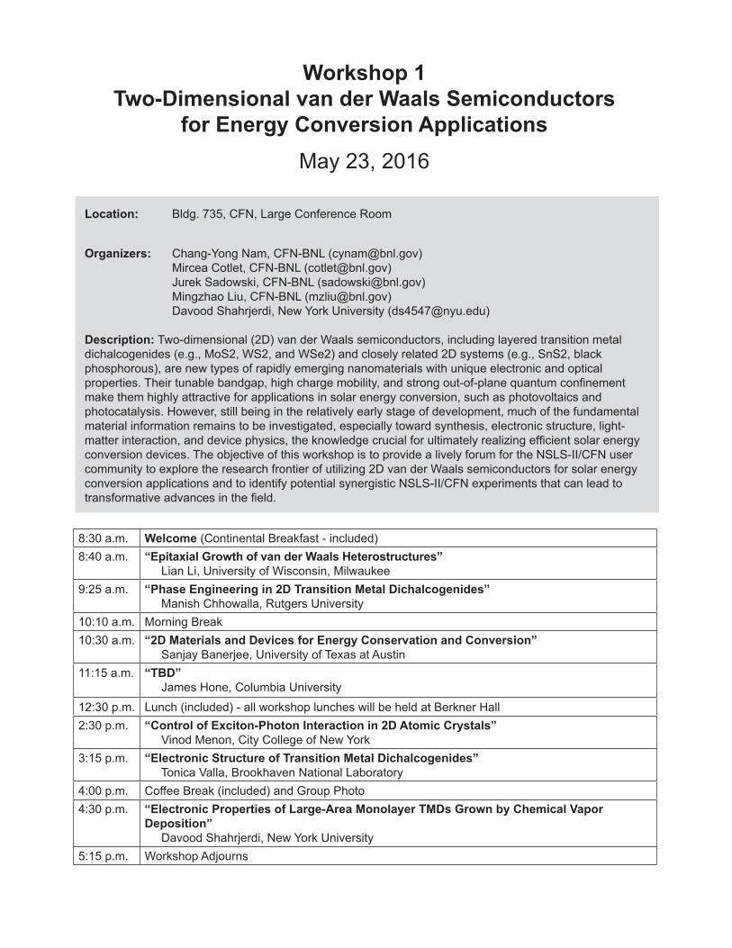
Workshop 1Two-Dimensional van der Waals Semiconductors
for Energy Conversion ApplicationsMay 23, 2016
Location: Bldg. 735, CFN, Large Conference Room
Organizers: Chang-Yong Nam, CFN-BNL ([email protected]) Mircea Cotlet, CFN-BNL ([email protected]) Jurek Sadowski, CFN-BNL ([email protected]) Mingzhao Liu, CFN-BNL ([email protected]) Davood Shahrjerdi, New York University ([email protected]) Description: Two-dimensional (2D) van der Waals semiconductors, including layered transition metal dichalcogenides (e.g., MoS2, WS2, and WSe2) and closely related 2D systems (e.g., SnS2, black phosphorous), are new types of rapidly emerging nanomaterials with unique electronic and optical properties. Their tunable bandgap, high charge mobility, and strong out-of-plane quantum confinement make them highly attractive for applications in solar energy conversion, such as photovoltaics and photocatalysis. However, still being in the relatively early stage of development, much of the fundamental material information remains to be investigated, especially toward synthesis, electronic structure, light-matter interaction, and device physics, the knowledge crucial for ultimately realizing efficient solar energy conversion devices. The objective of this workshop is to provide a lively forum for the NSLS-II/CFN user community to explore the research frontier of utilizing 2D van der Waals semiconductors for solar energy conversion applications and to identify potential synergistic NSLS-II/CFN experiments that can lead to transformative advances in the field.
8:30 a.m. Welcome (Continental Breakfast - included)8:40 a.m. “Epitaxial Growth of van der Waals Heterostructures”
Lian Li, University of Wisconsin, Milwaukee9:25 a.m. “Phase Engineering in 2D Transition Metal Dichalcogenides”
Manish Chhowalla, Rutgers University10:10 a.m. Morning Break10:30 a.m. “2D Materials and Devices for Energy Conservation and Conversion”
Sanjay Banerjee, University of Texas at Austin11:15 a.m. “TBD”
James Hone, Columbia University12:30 p.m. Lunch (included) - all workshop lunches will be held at Berkner Hall2:30 p.m. “Control of Exciton-Photon Interaction in 2D Atomic Crystals”
Vinod Menon, City College of New York3:15 p.m. “Electronic Structure of Transition Metal Dichalcogenides”
Tonica Valla, Brookhaven National Laboratory4:00 p.m. Coffee Break (included) and Group Photo4:30 p.m. “Electronic Properties of Large-Area Monolayer TMDs Grown by Chemical Vapor
Deposition” Davood Shahrjerdi, New York University
5:15 p.m. Workshop Adjourns

Agendas
8:40 a.m. “Epitaxial Growth of van der Waals Heterostructures” Lian Li, University of Wisconsin, MilwaukeeThe successful experimental isolation of graphene in 2004 has propelled the study of layered materials, characterized by anisotropic covalent intra-layer and van der Waals (vdW) inter-layer bonding. Furthermore, vdW heterostructures of these layered compounds, formed by either mechanical assembly or epitaxial growth, provide a “bottom up” avenue for “materials by design” to achieve enhanced functionalities beyond the limitation of their bulk (or monolayer) counterparts.In this talk, I will give a summary of our work on the epitaxial growth and atomic scale characterization of three classes of vdW heterostructures: 1) topological insulators Bi2Se3 and Bi2Te3 on epitaxial graphene, 2) superconductor FeSe on SrTiO3; and 3) semiconductors MoS2 and WS2 on SiO2. Our findings reveal unique challenges for the epitaxial growth of these vdW materials, as well as opportunities for engineering their physical and electronic properties by strain and electrical field.
9:25 a.m. “Phase Engineering in 2D Transition Metal Dichalcogenides” Manish Chhowalla, Rutgers University Two-dimensional transition metal dichalcogenides (2D TMDs) — whose generalized formula is MX2, where M is a transition metal of groups 4–7 and X is a chalcogen — consist of over 40 compounds. Complex metal TMDs assume the 1T phase where the transition metal atom coordination is octahedral. The 2H phase is stable in semiconducting TMDs where the coordination of metal atoms is trigonal prismatic. High performance of electronic and opto-electronic devices have been demonstrated with semiconducting TMDs while interesting condensed matter effects such as charge density waves and superconductivity have been observed in bulk metallic 1T phase TMDs. However, stability issues have hampered the study of interesting phenomena in two-dimensional 1T phase TMDs. Recently there has been a surge of activity in developing methodology to reversibly convert 2D 2H phase TMDs to 1T phase. In contrast with typical phase transformation conditions involving pressure and temperature, phase conversion in TMDs involves transformation by chemistry at room temperature and pressure. Using this method, we are able to convert 2H phase 2D TMDs to the 1T phase or locally pattern the 1T phase on 2H phase 2D TMDs. The chemically converted 1T phase 2D TMDs exhibit interesting properties that are being exploited for catalysis for hydrogen evolution reaction, source and drain electrodes in high performance field effect transistors, and as electrodes for energy storage. In this contribution, I will summarize the key properties of 2D 1T phase TMDs and their applications as electrodes for energy and electronics.
10:30 a.m. “2D Materials and Devices for Energy Conservation and Conversion” Sanjay Banerjee, University of Texas at Austin
Transition metal dichalcogenides (TMD) have opened up avenues in ultra-low power beyond-CMOS logic and memory device concepts involving single/many-particle 2D-2D tunneling showing negative differential resistance, and topological insulators (TI) show promise for spintronics. We will discuss CVD and MBE growth of TMDs such as MoS2, WSe2, MoTe2 and ReS2, and schemes for doping and ohmic contact formation to these materials. Novel low power logic and memory devices possible in 2D materials will be discussed. MBE of TIs such as Bi2Se3 which show spin-helical locking will be discussed for novel logic and non-volatile memory applications. For energy conversion, we will discuss initial efforts in incorporating graphene with Si for metal-insulator-semiconductor solar cells. Graphene could replace ITO front contacts.

2:30 p.m. “Control of Exciton-Photon Interaction in 2D Atomic Crystals” Vinod Menon, City College of New York
Two-dimensional (2D) atomic crystals have emerged as a very attractive class of photonic material due to the unprecedented strength in its interaction with light. In this talk I will discuss approaches to enhance the strength of this interaction even further using microcavities, plasmonic antenna structures and metamaterials. Specifically I will discuss enhancement of spontaneous emission, formation of strongly coupled exciton-photon quasiparticles and enhanced nonlinear optical response from 2D transition metal dichalcogenides (TMD) embedded in microcavities. Potential applications of such structures with controlled exciton-photon interaction and the use of unique valley properties in these TMDs will also be addressed.
3:15 p.m. “Electronic Structure of Transition Metal Dichalcogenides” Tonica Valla, Brookhaven National Laboratory
The transition metal dichalcogenides (TMD) form a big family of layered compounds with immensely diverse electronic properties, both in the bulk and in thin layers form, often involving ordered phases, such as CDW and superconductivity, or topological phases such as Weyl semimetals and topological insulators. Tightly intertwined with the structural variations, their electronic properties represent an ideal playground for exploring the quantum degrees of freedom of electrons and offer a great potential for new electronic and optical applications. Here, we will present several recent examples of TMD’s exotic phases.
4:30 p.m. “Electronic Properties of Large-Area Monolayer TMDs Grown by Chemical Vapor Deposition” Davood Shahrjerdi, New York University
Large-area synthesis of device-quality transition metal dichalcogenides (TMDs) is essential for the transformation of the basic science studies into viable device technologies. In this talk, we discuss synthesis of large monolayer MoS2 and WS2 using chemical vapor deposition (CVD). In particular, we present the electronic and optical properties of these materials and devices studied by a number of methods including photoluminescence, Raman spectroscopy, and temperature dependent transport measurements.
Agendas
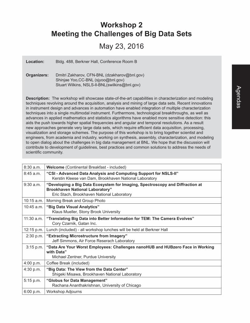
Workshop 2Meeting the Challenges of Big Data Sets
May 23, 2016
Location: Bldg. 488, Berkner Hall, Conference Room B
Organizers: Dmitri Zakharov, CFN-BNL ([email protected]) Shinjae Yoo,CC-BNL ([email protected]) Stuart Wilkins, NSLS-ll-BNL([email protected])
Description: The workshop will showcase state-of-the-art capabilities in characterization and modeling techniques revolving around the acquisition, analysis and mining of large data sets. Recent innovations in instrument design and advances in automation have enabled integration of multiple characterization techniques into a single multimodal instrument. Furthermore, technological breakthroughs, as well as advances in applied mathematics and statistics algorithms have enabled more sensitive detection: this aids the push towards higher spatial frequencies and angular and temporal resolutions. As a result new approaches generate very large data sets, which require efficient data acquisition, processing, visualization and storage schemes. The purpose of this workshop is to bring together scientist and engineers, from academia and industry, working on synthesis, assembly, characterization, and modeling to open dialog about the challenges in big data management at BNL. We hope that the discussion will contribute to development of guidelines, best practices and common solutions to address the needs of scientific community.
8:30 a.m. Welcome (Continental Breakfast - included)8:45 a.m. “CSI - Advanced Data Analysis and Computing Support for NSLS-II”
Kerstin Kleese van Dam, Brookhaven National Laboratory9:30 a.m. “Developing a Big Data Ecosystem for Imaging, Spectroscopy and Diffraction at
Brookhaven National Laboratory” Eric Stach, Brookhaven National Laboratory
10:15 a.m. Morning Break and Group Photo10:45 a.m. “Big Data Visual Analytics”
Klaus Mueller, Stony Brook University
11:30 a.m. “Translating Big Data into Better Information for TEM: The Camera Evolves” Cory Czarnik, Gatan Inc.
12:15 p.m. Lunch (included) - all workshop lunches will be held at Berkner Hall 2:30 p.m. “Extracting Microstructure from Imagery”
Jeff Simmons, Air Force Reserach Laboratory 3:15 p.m. “Data Are Your Worst Employees: Challenges nanoHUB and HUBzero Face in Working
with Data” Michael Zentner, Purdue University
4:00 p.m. Coffee Break (included)4:30 p.m. “Big Data: The View from the Data Center”
Shigeki Misawa, Brookhaven National Laboratory5:15 p.m. “Globus for Data Management”
Rachana Ananthakrishnan, University of Chicago6:00 p.m. Workshop Adjourns
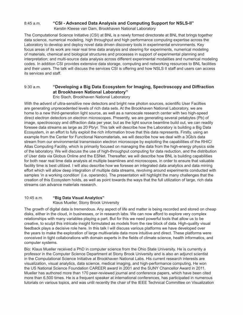
8:45 a.m. “CSI - Advanced Data Analysis and Computing Support for NSLS-II” Kerstin Kleese van Dam, Brookhaven National LaboratoryThe Computational Science Initiative (CSI) at BNL is a newly formed directorate at BNL that brings together data science, numerical modeling, high throughput and high performance computing expertise across the Laboratory to develop and deploy novel data driven discovery tools in experimental environments. Key focus areas of its work are near real time data analysis and steering for experiments, numerical modeling of materials, chemical and biological structures and processes in support of experimental planning and interpretation; and multi-source data analysis across different experimental modalities and numerical modeling codes. In addition CSI provides extensive data storage, computing and networking resources to BNL facilities and their users. The talk will discuss the services CSI is offering and how NSLS II staff and users can access its services and staff.
9:30 a.m. “Developing a Big Data Ecosystem for Imaging, Spectroscopy and Diffraction at Brookhaven National Laboratory” Eric Stach, Brookhaven National LaboratoryWith the advent of ultra-sensitive new detectors and bright new photon sources, scientific User Facilties are generating unprecedented levels of rich data sets. At the Brookhaven National Laboratory, we are home to a new third-generation light source, as well as a nanoscale research center with two high-speed direct electron detectors on electron microscopes. Presently, we are generating several petabytes (Pb) of image, spectroscopy and diffraction data per year, but as the light source beamline build out, we can readily foresee data streams as large as 20 Pb/yr. This talk will describe how the Laboratory is building a Big Data Ecosystem, in an effort to fully exploit the rich information trove that this data represents. Firstly, using an example from the Center for Functional Nanomaterials, we will describe how we deal with a 3Gb/s data stream from our environmental transmission electron microscope by exploiting the capabilities of the RHIC/Atlas Computing Facility, which is primarily focused on managing the data from the high-energy physics side of the laboratory. We will discuss the use of high-throughput computing for data reduction, and the distribution of User data via Globus Online and the ESNet. Thereafter, we will describe how BNL is building capabilities for both near real time data analysis at multiple beamlines and microscopes, in order to ensure that valuable facility time is best utilized. I will also describe how we foresee an integrated data analytics and data mining effort which will allow deep integration of multiple data streams, revolving around experiments conducted with samples ‘in a working condition’ (i.e. operando). The presentation will highlight the many challenges that the creation of this Ecosystem holds, as well as point towards the ways that the full utilization of large, rich data streams can advance materials research.
10:45 a.m. “Big Data Visual Analytics” Klaus Mueller, Stony Brook UniversityThe growth of digital data is tremendous. Any aspect of life and matter is being recorded and stored on cheap disks, either in the cloud, in businesses, or in research labs. We can now afford to explore very complex relationships with many variables playing a part. But for this we need powerful tools that allow us to be creative, to sculpt this intricate insight formulated as models from the raw block of data. High-quality visual feedback plays a decisive role here. In this talk I will discuss various platforms we have developed over the years to make the exploration of large multivariate data more intuitive and direct. These platforms were conceived in tight collaborations with domain experts in the fields of climate science, health informatics, and computer systems.Bio: Klaus Mueller received a PhD in computer science from the Ohio State University. He is currently a professor in the Computer Science Department at Stony Brook University and is also an adjunct scientist in the Computational Science Initiative at Brookhaven National Labs. His current research interests are visualization, visual analytics, data science, medical imaging, and high-performance computing, He won the US National Science Foundation CAREER award in 2001 and the SUNY Chancellor Award in 2011. Mueller has authored more than 170 peer-reviewed journal and conference papers, which have been cited more than 6,500 times. He is a frequent speaker at international conferences, has participated in numerous tutorials on various topics, and was until recently the chair of the IEEE Technical Committee on Visualization

Agendas
and Computer Graphics. He is also back on the editorial board of IEEE Transactions on Visualization and Computer Graphics and he is a senior member of the IEEE. For more information, please see http://www.cs.sunysb.edu/~mueller
11:30 a.m. “Translating Big Data into Better Information for TEM: The Camera Evolves” Cory Czarnik, Gatan Inc.As we transition from the previous generation of cameras and detectors (e.g., CCD based sensors, relatively slow frame rates, binned images to improve frame rate) to the current generation of cameras (large format CMOS detectors, video-like frame rates and extensive in-situ imaging), the demands on data workflow and data management are growing exponentially. Historically, it had only been practical to record a “picture” of an event in the TEM (e.g., VHS tape, screen capture software, etc.) whereas today’s camera systems are capable of storing the data in each (of perhaps 16M) pixel(s) at tens of frames per second directly to disk for offline quantitative analysis. This is facilitated by the rapid increase in computational power, data transfer efficiency, and data storage capabilities at the same time that the cost of these capabilities approaches something that can be incorporated into a single (albeit high end) PC with a commercial operating system. This has opened up many new applications including identifying fine detail in structural biology specimens (including the recent Zika virus), 4D STEM application to strain mapping in materials, sub-ms temporal resolution for in-situ reaction studies, and analysis of beam-sensitive zeolite and metal-organic framework samples as well as simply improving the usability of cameras for “picture taking” with fast frame drift correction of images.It is increasingly clear that a streamlined, robust, yet simple method of managing and analyzing large data sets needs to be developed in parallel with the applications themselves. For example, the structural biology community is currently employing direct detection cameras that output 80Gb/sec from the camera that is subsequently processed and reduced in size in order to make it useful for quick-turn analysis. While it may be straightforward to use a “brute force” method of storing, moving, and analyzing a single data set to demonstrate proof of concept for a given application, optimizing the workflow for each application will be required for widespread adoption and implementation.
2:30 p.m. “Extracting Microstructure from Imagery” Jeff Simmons, Air Force Research LaboratoryMaterials Science is somewhat unique in that microscopic observations are used to infer an “idealized structure” of a material that is then used in subsequent quantitative modeling of material behavior. That is, the “real” representation of a structure is a cognitive perception within the researcher’s mind, as opposed to one directly related to phenomenology. Complicating matters, when we speak of “microstructure,” we often mean some sort of nebulously defined statistical description of the structure, whose characteristics we intuitively recognize as part of our perception, but that require some thought when automating by computers. In this work, we model microstructure of a continuous fiber composite as a continuous “field variable” that describes the local shearing, rotation, dilation, and contraction of the fibers embedded in the matrix. Since the model is local, we are able to capture the statistical behavior of the structure by variations in the field from point to point. But, a fair amount of processing is necessary to convert image data to a field variable: extraction of fiber center positions, association of fibers through multiple images to assemble into 3-D objects, from which control points for fitting a field model may be employed. Subsequent analysis allows for identification of the various features of the fields. Since the model is local, it is also possible to use anomaly testing to separate anomalous from typical features. This presentation will give the current state of our efforts with continuous fiber SiC/SiC composites.

3:15 p.m. “Data Are Your Worst Employees: Challenges nanoHUB and HUBzero Face in Working with Data” Michael Zentner, Purdue UniversitynanoHUB.org has reached a point where it serves more than 1.4 million visitors annually, runs more than 800,000 simulations annually, and has a proven large impact in both research and education. Recently the nanoHUB community has asked for nanoHUB to support not only simulation but also working with data resources. Like employees, data are resources necessary for getting the job done. Data serve essential roles for analyzing impact retrospectively, taking immediate tactical action, or strategically planning the future. Unlike employees, we do not get to choose our data. Rather, they or the situation that creates them are placed upon us; and it is our job to learn how to manage these data to extract the value they contain. This talk will provide a general introduction to nanoHUB, and then will focus on several traits of data that are analogous to those of bad employees, with examples from applications of nanoHUB and and other HUBzero sites in the domains of nano materials safety, medical informatics, and hub usage information. A data exploration environment called IDENT will be discussed as an initial effort from nanoHUB to work with ill-structured and ill-behaved data. IDENT also serves as a graphical approach to experimental and simulation space exploration that can be used to drive underlying computations and experiment.
4:30 p.m. “Big Data: The View from the Data Center” Shigeki Misawa, Brookhaven National LaboratoryOver the past 17 years, the RACF (now part of the BNL Scientific Data and Computing Center), has provided support for compute and storage for the three “big data” scientific experiments at the lab. These experiments, PHENIX and STAR at the Relativistic Heavy Ion Collider (RHIC) and ATLAS at the Large Hadron Collider (LHC), are representative of experiments in scientific fields with long histories in big data. As scientific research moves into the era of “ubiquitous” big data, experiments in many other fields are joining the ranks of big data participants. Although there are commonalities between the traditional big data experiments and new big data experiments, there are also many fundamental differences. This presentation discusses the computational and storage challenges that lie ahead, as well as possible solutions, as seen from the data center perspective in this new era of big data.
5:15 p.m. “Globus for Data Management” Rachana Ananthakrishnan, University of ChicagoWith rapid increase in the data that is generated and requires processing, sharing, tracking and archiving, there is a need for robust solutions for managing data at such scale across it’s lifecycle. This talk will present use of Globus, a software-as-a-service developed at, and operated by, the University of Chicago, for research data management. Globus provides high speed, secure file transfer; file sharing directly from institutional storage systems; and data publication capabilities. The talk will cover an overview and demonstration of Globus, discuss exemplar applications where Globus is leveraged for data management including at beamlines at Advanced Photon Source, and illustrate use of Globus APIs for integration with workflows and pipelines.
Agendas
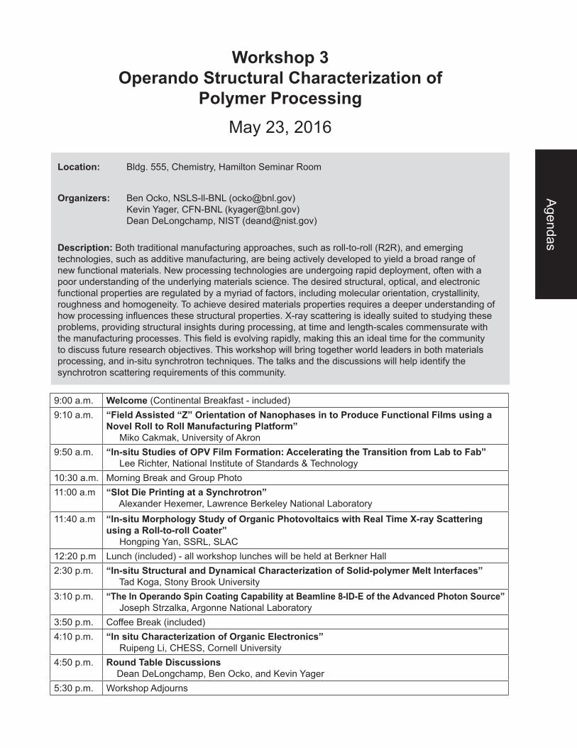
Workshop 3Operando Structural Characterization of
Polymer ProcessingMay 23, 2016
Location: Bldg. 555, Chemistry, Hamilton Seminar Room
Organizers: Ben Ocko, NSLS-ll-BNL ([email protected]) Kevin Yager, CFN-BNL ([email protected]) Dean DeLongchamp, NIST ([email protected]) Description: Both traditional manufacturing approaches, such as roll-to-roll (R2R), and emerging technologies, such as additive manufacturing, are being actively developed to yield a broad range of new functional materials. New processing technologies are undergoing rapid deployment, often with a poor understanding of the underlying materials science. The desired structural, optical, and electronic functional properties are regulated by a myriad of factors, including molecular orientation, crystallinity, roughness and homogeneity. To achieve desired materials properties requires a deeper understanding of how processing influences these structural properties. X-ray scattering is ideally suited to studying these problems, providing structural insights during processing, at time and length-scales commensurate with the manufacturing processes. This field is evolving rapidly, making this an ideal time for the community to discuss future research objectives. This workshop will bring together world leaders in both materials processing, and in-situ synchrotron techniques. The talks and the discussions will help identify the synchrotron scattering requirements of this community.
9:00 a.m. Welcome (Continental Breakfast - included)9:10 a.m. “Field Assisted “Z” Orientation of Nanophases in to Produce Functional Films using a
Novel Roll to Roll Manufacturing Platform” Miko Cakmak, University of Akron
9:50 a.m. “In-situ Studies of OPV Film Formation: Accelerating the Transition from Lab to Fab” Lee Richter, National Institute of Standards & Technology
10:30 a.m. Morning Break and Group Photo11:00 a.m “Slot Die Printing at a Synchrotron”
Alexander Hexemer, Lawrence Berkeley National Laboratory11:40 a.m “In-situ Morphology Study of Organic Photovoltaics with Real Time X-ray Scattering
using a Roll-to-roll Coater” Hongping Yan, SSRL, SLAC
12:20 p.m Lunch (included) - all workshop lunches will be held at Berkner Hall2:30 p.m. “In-situ Structural and Dynamical Characterization of Solid-polymer Melt Interfaces”
Tad Koga, Stony Brook University3:10 p.m. “The In Operando Spin Coating Capability at Beamline 8-ID-E of the Advanced Photon Source”
Joseph Strzalka, Argonne National Laboratory3:50 p.m. Coffee Break (included)4:10 p.m. “In situ Characterization of Organic Electronics”
Ruipeng Li, CHESS, Cornell University4:50 p.m. Round Table Discussions
Dean DeLongchamp, Ben Ocko, and Kevin Yager5:30 p.m. Workshop Adjourns
9:10 a.m. “Field Assisted “Z” Orientation of Nanophases in to Produce Functional Films using a Novel Roll to Roll Manufacturing Platform” Miko Cakmak, University of Akron
Electric1,2, Magnetic3, and Thermal gradient5,6 fields are three important methods used in Field Assisted Self Assembly (FASA) of polymer blends, block copolymers, liquid crystals and polymer nanocomposites. These assisted assembly techniques have been used in laboratory scale, but for potential applications such as flexible electronics7, membranes8, supercapacitors9, fuel cells10, photovoltaic’s etc. a large scale manufacturing platform is needed.We introduce a novel roll to roll process developed in our laboratories to achieve “Z-direction” alignment of nanostructural units. A 70 ft line was designed which uses a casting system to deposit desired thickness of liquid such as a monomer and/or polymer solution up to 6” wide on a flexible substrate using a doctor blade system and flow coating system to deposit thin films. The substrate is then carried by pretensioned steel belt through an electric field application zone which consists of a parallel electrode sitting on top of the steel belt with the solution cast film passing below it. The electric field applied can be a DC, AC or a biased AC, hence using the various fields we can maximize the orientation by increasing the dielectric contrast between the particles and the matrix.If orientation and self-assembly through magnetic field is desired, the second tool located downstream is activated. This electromagnet is capable of applying magnetic fields up to 2.2 T to the material supported by a flexible substrate through the opposing poles. This line also contains a movable UV lamp which can be used to freeze the structure of required morphology using photocurable resin and could also be used to etch one phase of a polymer blend or block copolymer after electric field or magnetic field application zones.The final tool that is built on this machine is the Thermal Alignment zone. It is designed to apply a “line of heat” oriented transverse to the line direction at 9 different zones. In each zone the material may be subjected to a temperature gradient in the machine direction through a successive heating and cooling units. The temperature gradients can be created using conduction or radiation.Electric and magnetic field alignment of particles and polymer chains is studied through real time birefringence measurement, to determine various parameters effecting the orientation of particles/phases inside a polymeric film under the magnetic or electric field. The birefringence system is based on the solution drying process developed in our lab11.References: (1) Park, C.; Robertson, R. E. Materials Science and Engineering: A 1998, 257, 295-311.(2) Kyrylyuk, A.; Zvelindovsky, A.; Sevink, G. Macromolecules 2002, 35, 1473-1476. (3) Osuji, C.; Ferreira, P. J.; Mao, G.; Ober, C. K.; Vander Sande, J. B.; Thomas, E. L. Macromolecules 2004, 37, 9903-9908. (4) Takahashi, T.; Murayama, T.; Higuchi, a; Awano, H.; Yonetake, K. Carbon 2006, 44, 1180-1188. (5) Mita, K.; Tanaka, H.; Saijo, K.; Takenaka, M.; Hashimoto, T. Macromolecules 2008, 41, 6787-6792. (6) Liu, C.-Y.; Bard, A. J. Chemistry of Materials 2000, 12, 2353-2362. (7) Wong, W. A. Salleo,Flexible Electronics: Materials and Applications ,2009. Springer (8) Oren, Y.; Freger, V.; Linder, C. Journal of Membrane Science 2004, 239, 17-26. (9) Park, B.; Im, K.-J.; Cho, K.; Kim, S. Organic Electronics 2008, 9, 878-882. (10) Gasa, J. V.; Weiss, R. a.; Shaw, M. T. Journal of Membrane Science 2008, 320, 215-223. (11) Unsal, E.; Drum, J.; Yucel, O.; Nugay, I. I.; Yalcin, B.; Cakmak, M. The Review of scientific instruments 2012, 83, 025114.
9:50 a.m. “In-situ Studies of OPV Film Formation: Accelerating the Transition from Lab to Fab” Lee Richter, National Institute of Standards & Technology
Solution processing of electrically active layers is a promising route to sustainable manufacturing of functional components on diverse substrates such as flexible foils and textiles. Typically, solution processing does not result in the thermodynamic equilibrium form; instead metastable, kinetically trapped structures dominate. This allows great flexibility in the ability to tailor film structure (and performance) by processing details. The sensitivity of structure and performance to processing is clearly manifest in the fabrication of bulk heterojunction (BHJ) active layers for organic photovoltaics. Organic photovoltaic devices are a promising

Agendas
route to lower costs via roll-to-roll manufacturing. In a BHJ, nano-scale phase separation into nominally bicontinuous donor and acceptor rich regions enables both exciton dissociation and charge extraction. The performance of BHJ based devices is a strong function of the active layer structure and the optimized device structure is, in general, not the equilibrium structure. Recently it has become common to optimize BHJ film formation by introducing small amounts of processing additives. However, the mechanisms by which these additives effect the film formation are not known. We present results from the use of labscale photon based techniques, such as spectroscopic ellipsometry and photoluminescence and synchrotron based grazing incidence x-ray scattering (both wide angle and small angle) on the time evolution of films cast by blade coating, a material conservative model for scalable manufacturing processes. The in-situ measurements provide detailed insights into film thickness, composition, and microstructure. We will discuss highlights from studies of the additive effect in film formation of both polymer and small molecule based BHJs. Multiple mechanisms are revealed with common themes related to control of aggregation through solvent quality and control of growth kinetics via plasticization. We observe that, when elevated solution temperatures are required, significant differences between spin coating and isothermal deposition such as blade coating can arise. We demonstrate that isothermal blade coating is an excellent prototyping tool for slot-die coating by establishing comparable morphologies for small piece blade coating and continuous web slot-die coating.
11:00 a.m. “Slot Die Printing at a Synchrotron” Alexander Hexemer, Lawrence Berkeley National Laboratory
In order to move closer and closer to real processing conditions of polymer thin films we installed a industrial level slot-die printer at our SAXS/WAXS beamline at the ALS. The slot-die printer has since been opened up to a wide variety of users and materials. We are able to print and measure the drying process in real-time in GISAXS and GIWAXS geometry. In addition we developed a data pipeline and analysis framework to handle, store and analyze the data. The goal was to provide real-time feedback to scientists during beamtime. HipGISAXS was used in a real time demonstration that married the slot-die printing with the data handling and processing capabilities at NERSC, and simulation capabilities of running at-scale simulations on Titan at OLCF. The demo involved the printing of organic photovoltaics using a slot-die printer. Over the span of 3 days many different organic photovoltaics were printed at the beamline and the crystal structure evolution during drying was recorded using GIWAXS. The entire progress of data collection, movement and fitting was monitored on a web dashboard.
11:40 a.m. “In-situ Morphology Study of Organic Photovoltaics with Real Time X-ray Scattering using a Roll-to-roll Coater” Hongping Yan, SSRL, SLAC
Performance of organic photovoltaics (OPVs) is extremely sensitive to the morphology of the bulk heterojunction (BHJ) active layer, which can be greatly impacted by the processing methods and conditions. It is not surprising that the optimized processing conditions for spin coating usually cannot be directly transferred to roll-to-roll (R2R) coating for mass volume production. In order to bridge the gap between laboratory scale and industrial scale development of OPV materials and processes for better materials design and morphology control, in-depth understanding of the morphology evolution of organic semiconductors is highly demanded. We have developed a R2R coater designed to be portable and adaptable so that it allows in-situ x-ray scattering during the R2R coating process on synchrotron beamlines. Multi-length scale morphology evolution information was obtained by implement this portable coater with different grazing-incidence scattering geometries, i.e. molecular packing and crystallization through wide-angle (GIWAXS) and phase separation through small-angle scattering (GISAXS). We have investigated the drying process and BHJ morphology evolution of the OPV blend systems based on either small molecule or polymeric donor and acceptor materials as a function of processing conditions. Exciting findings on processing-morphology-performance relation will be discussed for these model systems, and the knowledge is expected to greatly advance the understanding of morphology control of solution processed organic materials at scale, which is expect to benefit relevant broader polymer research fields as well.

2:30 p.m. “In situ Structural and Dynamical Characterization of Solid-polymer Melt Interfaces” Tad Koga, Stony Brook UniversityThe topic of this talk, ultrathin polymer films on solids, has been of vital interest in many traditional technologies as well as in new emerging nanotechnologies such as organic photovoltaics, semiconductor chips, and biosensors. There is now growing evidence that polymer chains irreversibly adsorb even onto weakly attractive solid surfaces, forming several nanometer-thick adsorbed polymer layers (“adsorbed nanolayers”). I present our recent X-ray and neutron scattering results on the structure and dynamics of the adsorbed nanolayers composed of various polymers (amorphous, semicrystalline, and blockpolymers) and their equilibrium pathway/conformation at planar and curved solid surfaces [1-7]. In addition, we found that the effects of the adsorbed nanolayers propagate into the film interior, resulting in long-range perturbations of the local structure/dynamics/property of ultrathin polymer films [1-3]. Furthermore, we have revealed that the adsorbed nanolayers play a vital role in the macroscopic stability of ultrathin polymer films [5]. Finally, I highlight the structure and dynamics of the adsorbed nanolayers formed onto nanoparticle surfaces that play crucial roles in the rheological and mechanical properties of polymer nanocomposites [7].[1] P. Gin et al., Phys. Rev. Lett., 109, 265501 (2012).
[2] N. Jiang et al., Macromolecules, 47, 2682 (2014).
[3] M. Asada et al., Soft Matter, 34, 6392 (2014).
[4] N. Jiang et al., Macromolecules 48, 1795 (2015).
[5] N. Jiang et al., Soft Matter, 2016, 12, 1801 (2016).
[6] M. Sen et al., ACS Macro Letter, 5, 504 (2016).
[7] N. Jiang et al., ACS Macro Letter, 4, 838 (2015).
3:10 p.m. “The In Operando Spin Coating Capability at Beamline 8-ID-E of the Advanced Photon Source” Joseph Strzalka, Argonne National Laboratory
Spin casting from solution is a ubiquitous and commercially important process for fabricating uniform, homogeneous polymer thin films. It is widely used in organic photovoltaic research, including the fabrication of the champion organic devices tracked in the NREL chart of Best Research-Cell Efficiencies, which significantly outperform devices manufactured by more scalable processes. Addressing this performance gap requires a better understanding of processing at both industrial and laboratory scale. In order to enable in operando Grazing-Incidence X-Ray Scattering studies of spin casting, we have developed at Beamline 8-ID-E a stable and robust spin coating sample environment for general use. Based on an air bearing spindle motor, the spin coater achieves rotational velocities up to 4000 rpm with only minimal angular broadening and can accommodate silicon wafers up to 100 mm in diameter in an inert atmosphere. Sample injection is automated and does not obstruct the field of view. A commercial optical reflectance instrument monitors the evolution of sample thickness during the spin-coating process. A tandem undulator source, vertically focused beam and the fast-framing capability of the Pilatus 1M detector allow temporal resolution of about 10 ms. Examples of in operando measurements in GISAXS and GIWAXS geometries will be presented. The spin coating sample environment is now available for General Users.

Agendas
4:10 p.m. “In situ Characterization of Organic Electronics” Ruipeng Li, CHESS, Cornell University
Solution-processed organic electronics have attracted considerable attention due to their high performance, low cost and easy manufacture. Achieving high performance requires that the microstructure and morphology of solution-cast thin films – that develops via nucleation and growth processes – exhibit a high degree of crystallinity with two-dimensional in-plane p-stacking, a low density of grain/domain boundaries exhibiting low crystallographic misorientation. Efforts to tune the microstructures and morphologies of solution-cast thin films require the more controllable casting processing and the more accessible in situ characterization methodology.I will present the efforts in CHESS to develop in situ x-ray scattering techniques for structural characterization. Multiple casting techniques including conventional casting methods in lab, such like drop-casting and spin-coating, and roll-2-roll processing, have been explored. The results reveal the relationship between the microstructure, morphology and the device performance and direct fine tuning of the casting processing for advanced organic electronic devices.
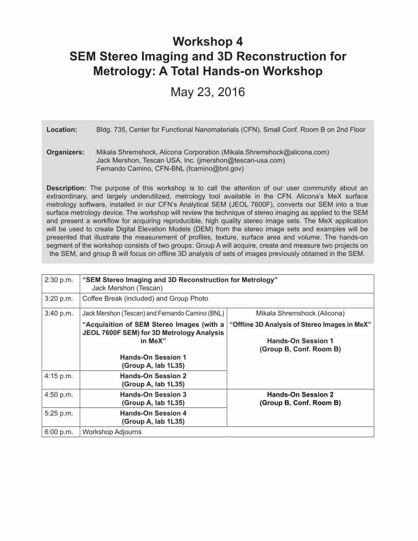
Workshop 4SEM Stereo Imaging and 3D Reconstruction for
Metrology: A Total Hands-on WorkshopMay 23, 2016
Location: Bldg. 735, Center for Functional Nanomaterials (CFN), Small Conf. Room B on 2nd Floor
Organizers: Mikala Shremshock, Alicona Corporation ([email protected]) Jack Mershon, Tescan USA, Inc. ([email protected]) Fernando Camino, CFN-BNL ([email protected]) Description: The purpose of this workshop is to call the attention of our user community about an extraordinary, and largely underutilized, metrology tool available in the CFN. Alicona’s MeX surface metrology software, installed in our CFN’s Analytical SEM (JEOL 7600F), converts our SEM into a true surface metrology device. The workshop will review the technique of stereo imaging as applied to the SEM and present a workflow for acquiring reproducible, high quality stereo image sets. The MeX application will be used to create Digital Elevation Models (DEM) from the stereo image sets and examples will be presented that illustrate the measurement of profiles, texture, surface area and volume. The hands-on segment of the workshop consists of two groups: Group A will acquire, create and measure two projects on the SEM, and group B will focus on offline 3D analysis of sets of images previously obtained in the SEM.
2:30 p.m. “SEM Stereo Imaging and 3D Reconstruction for Metrology” Jack Mershon (Tescan)
3:20 p.m. Coffee Break (included) and Group Photo
3:40 p.m. Jack Mershon (Tescan) and Fernando Camino (BNL)“Acquisition of SEM Stereo Images (with a JEOL 7600F SEM) for 3D Metrology Analysis
in MeX”
Hands-On Session 1(Group A, lab 1L35)
Mikala Shremshock (Alicona)“Offline 3D Analysis of Stereo Images in MeX”
Hands-On Session 1(Group B, Conf. Room B)
4:15 p.m. Hands-On Session 2(Group A, lab 1L35)
4:50 p.m. Hands-On Session 3(Group A, lab 1L35)
Hands-On Session 2(Group B, Conf. Room B)
5:25 p.m. Hands-On Session 4(Group A, lab 1L35)
6:00 p.m. Workshop Adjourns
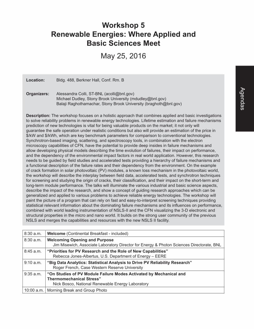
Agendas
Workshop 5Renewable Energies: Where Applied and
Basic Sciences MeetMay 25, 2016
Location: Bldg. 488, Berkner Hall, Conf. Rm. B
Organizers: Alessandra Colli, ST-BNL ([email protected]) Michael Dudley, Stony Brook University ([email protected]) Balaji Raghothamachar, Stony Brook University ([email protected]) Description: The workshop focuses on a holistic approach that combines applied and basic investigations to solve reliability problems in renewable energy technologies. Lifetime estimation and failure mechanisms prediction of new technologies is vital for being valuable products on the market; it not only will guarantee the safe operation under realistic conditions but also will provide an estimation of the price in $/kW and $/kWh, which are key benchmark parameters for comparison to conventional technologies. Synchrotron-based imaging, scattering, and spectroscopy tools, in combination with the electron microscopy capabilities of CFN, have the potential to provide deep insides in failure mechanisms and allow developing physical models describing the time evolution of failures, their impact on performance, and the dependency of the environmental impact factors in real world application. However, this research needs to be guided by field studies and accelerated tests providing a hierarchy of failure mechanisms and a functional description of the failure rates and their dependency from the environment. On the example of crack formation in solar photovoltaic (PV) modules, a known loss mechanism in the photovoltaic world, the workshop will describe the interplay between field data, accelerated tests, and synchrotron techniques for screening and studying the origin of cracks, their classification, and their impact on the short-term and long-term module performance. The talks will illuminate the various industrial and basic science aspects, describe the impact of the research, and show a concept of guiding research approaches which can be generalized and applied to various problems to achieve reliable energy technologies. The workshop will paint the picture of a program that can rely on fast and easy-to-interpret screening techniques providing statistical relevant information about the dominating failure mechanisms and its influences on performance, combined with world leading instrumentation of NSLS-II and the CFN visualizing the 3-D electronic and structural properties in the micro and nano world. It builds on the strong user community of the previous NSLS and merges the capabilities and resources with the new NSLS II facility.
8:30 a.m. Welcome (Continental Breakfast - included)8:30 a.m. Welcoming Opening and Purpose
Jim Misewich, Associate Laboratory Director for Energy & Photon Sciences Directorate, BNL8:45 a.m. “Priorities for PV Research and the Role of New Capabilities”
Rebecca Jones-Albertus, U.S. Department of Energy – EERE9:10 a.m. “Big Data Analytics: Statistical Analysis to Drive PV Reliability Research”
Roger French, Case Western Reserve University9:35 a.m. “On Studies of PV Module Failure Modes Activated by Mechanical and
Thermomechanical Stress” Nick Bosco, National Renewable Energy Laboratory
10:00 a.m. Morning Break and Group Photo

10:15 a.m. “Advanced Characterization of Surface Passivation and Passivated Contacts in Silicon Photovoltaics” Kristopher Davis, U.S. Photovoltaic Manufacturing Consortium
10:40 a.m. “Damage Mapping and Mechanism Discovery in Silicon Films and Wafers” Christopher Muhlstein, Georgia Institute of Technology
11:05 a.m. “Application of X-ray Topography Techniques to the Study of Defects and Strain in Solar Materials” Michael Dudley, Stony Brook University
11:35 a.m. “Spectroscopic X-ray Beam Induced Current: A Tool for Understanding Charge Motion in Semiconductors” John Smedley, Brookhaven National Laboratory
12:00 p.m. Discussion and Workshop Adjourns Klaus Attenkofer, Brookhaven National Laboratory
12:30 p.m. Lunch (included) - all workshop lunches will be held at Berkner Hall1:30 p.m. Facility Tour (for speakers and a limited number of participants), -
Photovoltaic Fields: NSERC Research Array and Long Island Solar, Farm: guided by John P. Looney and Robert Lofaro, National Synchrotron Light Source II: guided by Klaus Attenkofer, Center for Functional Nanomaterials: guided by Eric Stach
8:45 a.m. “Priorities for PV Research and the Role of New Capabilities” Rebecca Jones-Albertus, Solar Energy Technolgies Office, U.S. Department of Energy
The U.S. Department of Energy’s SunShot Initiative seeks to enable subsidy-free solar energy to be cost competitive with conventional energy sources. Here the technology metrics for photovoltaic module cost, efficiency and reliability that are needed to reach the SunShot goals will be discussed, in the context of existing and emerging PV technologies.To have the greatest continued impact on photovoltaic module as well as balance of system costs, SunShot’s Photovoltaics program is focusing on what we see as today’s largest technology R&D levers for cost reduction. Improved module reliability and performance prediction, for example, can significantly impact the balance of systems costs through lower cost of capital as well as increased energy output over the module lifetime. The potential impacts of innovations in PV module design, reductions in material and processing costs, and increases in cell and module performance on the cost of PV electricity will be discussed, as well as the role of new capabilities in enabling these innovations.
9:10 a.m. “Big Data Analytics: Statistical Analysis to Drive PV Reliability Research” Roger French, Case Western Reserve University
Degradation science1 combines physical and statistical approaches to examine degradation mechanisms and pathways in order to improve materials and reduce system failures. Degradation of PV modules involves slow and rare events and evolves over long time-frames and length scales; a characteristic of mesoscale science. Real-world studies under diverse environmental conditions must be integrated and cross-correlated with accelerated in-lab studies, using data science and analytics, to create a degradation pathway model incorporating the time and length scales that control the system’s lifetime behavior. Temporal analytics of time-series datastreams from PV power plants, including minute-by-minute power output (Pmp) and every 10 minutes I-V curve datastreams, provides new opportunities to understand the actual responses of PV modules under real-world climatic conditions and stressors, including the non-uniform illumination and other factors which are ignored in idealized, standards-based laboratory testing. These detailed diagnostic measures of real-world stressors will help attain the DOE SunShot goal of 50 year module lifetimes and allow for the growing contribution of PV power plants. This kind of un-biased, data-driven analytics, now possible using data science methodologies, represents a new front in our scientific studies of critically important and complex systems.
Agendas
Semi-supervised, generalized, structural equation modeling (semi-gSEM) is used to identify statistically significant pathway relationships in networks of physical mechanistic submodels and data-driven statistical submodels. The relationships and coupling strengths (βij) amongst variables are rank-ordered, and their temporal evolution, damage accumulation, and change points among mechanisms/mode are identified. Poly(ethylene terephthalate) (PET; used in PV module backsheets) and full PV module degradation will be discussed. 1. French, Roger H., Rudolf Podgornik, Timothy J. Peshek, Laura S. Bruckman, Yifan Xu, Nicholas R. Wheeler, Abdulkerim Gok, et al., 2015, “Degradation Science: Mesoscopic Evolution and Temporal Analytics of Photovoltaic Energy Materials,” Current Opinion in Solid State and Materials Science, Doi: 10.1016/j.cossms.2014.12.008
10:15 a.m. “Advanced Characterization of Surface Passivation and Passivated Contacts in Silicon Photovoltaics” Kristopher Davis, U.S. Photovoltaic Manufacturing Consortium
Crystalline silicon (c-Si) photovoltaics (PV) currently dominates the solar industry with over 93% market share. However, the majority of c-Si PV cells manufactured today are limited, in large part, by recombination occurring at the Si surfaces. Recent advances in surface passivation and passivated contacts have led to significant improvements in c-Si PV cells, enabling open-circuit voltages greater than 700 mV and efficiencies greater than 25%. As new passivation materials and deposition methods emerge, there is a critical need to develop characterization methods that: quantify recombination and resistive losses in these materials; and provide fundamental understanding of the influence of structure and composition on performance. This presentation provides a snapshot of passivation and passivated contact technology and avenues of research that can assist in pushing these materials to new heights.http://www.fsec.ucf.edu/people/bios/Davis.htm
10:40 a.m. “Damage Mapping and Mechanism Discovery in Silicon Films and Wafers” Christopher Muhlstein1 and Eric A. Stach2
1School of Materials Science and Engineering, Georgia Institute of Technology 2 Center for Functional Nanomaterials, Brookhaven National Laboratory
For decades silicon-based electronics, microelectromechanical systems (MEMS), and photovoltaics were thought to be immune to damage accumulation and subcritical crack growth mechanisms such as environmentally-assisted (stress corrosion) cracking and fatigue. Silicon’s purported immunity was a byproduct of its linear elastic constitutive behavior (i.e., no plastic deformation occurs at temperatures below its ductile to brittle transition of 565°C) and its rapidly forming, passivating oxide layer. However, the combination of small size and high loading frequencies in silicon-based MEMS revealed that silicon can, in fact, accumulate damage and exhibit delayed failures at stresses well below its fracture strength. In this presentation we will explore these damage accumulation mechanisms and how they were revealed using the unique electron microscopy tools at national lab user facilities. We will then illustrate their relevance to the viability of photovoltaic power plant installations and the critical role that synchrotron X-ray beamlines can play in quantitative mapping of damage in photovoltaic modules.

11:05 a.m. “Application of X-ray Topography Techniques to the Study of Defects and Strain in Solar Materials” Michael Dudley, Stony Brook University
Crystalline silicon photovoltaic (PV) modules are the predominant devices used in solar farms. The performance and lifetime of encapsulated silicon solar cells that constitute a module are a complex function of different variables from the manufacturing process and the module operational environment. Understanding the impact of various factors would greatly contribute to improving PV silicon-based renewable energy technologies. Among these factors, defects and strain in the silicon material play a critical role in determining the efficacy of the cells that make up the module. The application of X-ray topography can non-destructively provide information on the nature and distribution of structural defects such as dislocations, inclusions/precipitates, twins and low angle grain boundaries, etc. in the silicon material. Further by using a mesh/grid in the path of the incident/diffracted beam (i.e. X-ray reticulography) it is possible to trace the change in path of X-rays diffracted from for e.g. a strained region of crystal and quantitatively determine the full strain and thereby the stress tensor as a function of position inside the crystal. Thus, applying both X-ray topography and X-ray reticulography at each stage of the module manufacturing process enables understanding and lead to improved control of the processing sequence used to convert high purity silicon chunk into crystalline Si solar cells. Using the high intensity, broad energy range, high brightness and low divergent X-ray beam provided by a synchrotron source such as NSLS-II, we can rapidly and non-destructively image and characterize defects and strains at micron resolution. Direct imaging of the silicon material encapsulated in the cell will also allow in situ monitoring to study the generation, interaction and propagation of defects during device operation or for XBIC studies to identify performance limiting defects. In this presentation, an overview of X-ray topography and X-ray reticulography will be provided along with appropriate experimental results from packaged silicon devices and solar cells.
Agendas
Workshop 6The Earth Laboratory: Experimental and Computational
Tools and Infrastructure for Cross-cutting Earth SciencesMay 25, 2016
Location: Bldg. 735, Center for Functional Nanomaterials (CFN), Large Conference Room
Organizers: Lars Ehm, Stony Brook University/BNL ([email protected]) Donald Weidner, Stony Brook University ([email protected]) John Parise, Stony Brook University/BNL ([email protected]) Richard Reeder, Stony Brook University ([email protected]) Martin Schoonen, DJ-BNL ([email protected])
Description: The laboratory based Earth Science community has been an early adopter of the experimental capabilities provided by synchrotron sources. Conducting in situ, time and spatially resolved X-ray experiments on complex natural samples and samples at variable environmental conditions have greatly enhanced our understanding of the structure, processes, and evolution of the Earth and other Planets. The emerging topics in Earth and Planetary Science as well as long standing scientific questions about the Earth are highly complex and can only be tackled through combined computational and experimental effort; employing multiple complementary experimental and theoretical tools. The user facilities at Brookhaven National Laboratory - the National Synchrotron Light Source II (NSLS-II), the Center for Functional Nanomaterials (CFN), and the Computational Science Center (CSC) - could provide the foundation for such a thrust. The workshop will connect leading scientists in Earth and Planetary Science with the world-class scientists at BNL’s user facilities. The goal of the workshop is to: (i) identify the scientific challenges that would lead to a paradigm change in our understanding of structure, processes, and evolution of Planets and the Earth, (ii) determine development needs for experimental and computational tools at BNL’s user facilities, and (iii) to define the needed cross-cutting infrastructure (e.g. support laboratories, proposal access etc.) to enhance the access to different beamlines at NSLS-II, the experimental capabilities at the CFN and the computational resources at the CSC.
2:45 p.m. Welcome 3:00 p.m. “Evidence for and Implications of a Viscosity Increase in the Mid Mantle”
Vedan Lekic, University of Maryland3:30 p.m. “Fracturing OlIvine via Shrinkage Cracks: Evidence from Dynamic Microtomography”
Wenlu Zhu, University of Maryland 4:00 p.m. Coffee break (included) and Group Photo
4:30 p.m. “New Opportunities for Studying Planetary Returned Samples” Scott McLennan, Stony Brook University
5:00 p.m. “High-Energy X-rays for Characterizing Complex Materials” Eric Dooryhee, NSLS-ll, Brookhaven National Laboratory
5:10 p.m. “X-ray Spectroscopy with Sub-micron Spatial Resolution for Earth and Planetary Materials” Juergen Thieme, NSLS-ll, Brookhaven National Laboratory
5:20 p.m. “Present and Near-future Scientific Capabilities for the Hard X-ray Nanoprobe (HXN) at NSLS-II” Yong Chu, NSLS-ll, Brookhaven National Laboratory

5:30 p.m. “IXS Beamline, Capabilities and Opportunities” Yong Cai, NSLS-ll, Brookhaven National Laboratory
5:40 p.m. “ISS Beamline, Capabilities and Opportunities” Klaus Attenkofer, NSLS-ll, Brookhaven National Laboratory
5:50 p.m. Discussion and Concluding Remarks
6:00 p.m. Workshop Adjourns
3:00 p.m. “Evidence for and Implications of a Viscosity Increase in the Mid Mantle” Vedan Lekic, University of Maryland
The viscosity structure of Earth’s deep mantle affects the thermal evolution of Earth, the ascent of mantle plumes, settling of subducted oceanic lithosphere, and the mixing of compositional heterogeneities in the mantle. Based on a reanalysis of the long-wavelength non-hydrostatic geoid, we infer viscous layering of the mantle using a method that allows us to avoid a priori assumptions about its variation with depth. We detect an increase in viscosity at 800- to 1200-kilometers depth, far greater than the depth of the mineral phase transformations that define the mantle transition zone. The viscosity increase is coincident in depth with regions where seismic tomography has imaged slab stagnation, plume deflection, and changes in large-scale structure and offers a simple explanation of these phenomena. Explaining the origin of this viscosity increase represents a new challenge to the mineral physics community.
3:30 p.m “Fracturing OlIvine via Shrinkage Cracks: Evidence from Dynamic Microtomography” Wen-lu Zhu, University of Maryland
Sequestering CO2 via mineral carbonation has generated lots of interests owing to the abundance of silicate rocks and the permanence of the carbonated solids. However, the usefulness of ultramafic rocks as carbon storage hinges on the feasibility of creating and maintaining reactive surface area. Using synchrotron based X-ray micro- and nano-tomography techniques, we measured the evolution of the 3-dimensional pore geometry of an olivine aggregate undergoing mineral carbonation. We demonstrate that fracturing of the host rock can be achieved during carbonation reactions without additional energy input. Shrinkage cracking is responsible for producing the cracks. The polygonal pattern associated with shrinkage cracks is more consistent with fracture patterns observed in silicate rocks that undergo natural weathering. This experimentally tested mechanism of reaction-induced fracturing has important implications in geological carbon sequestration research.
4:30 p.m. “New Opportunities for Studying Planetary Returned Samples at Brookhaven National Laboratory” S.M. McLennan1, J.A. Hurowitz1, M.A.A. Schoonen2, J. Thieme3 1 Department of Geosciences, Stony Brook University; 2 Environment, Biology, Nuclear Science and Nonproliferation, Brookhaven National Laboratory; 3 National Synchrotron Light Source-ll, Brookhaven National Laboratory
A wide variety of synchrotron studies have proven invaluable in the study of extraterrestrial planetary materials, including meteorites, lunar samples, comets, asteroids, solar wind and interplanetary dust. Over the next two decades, new opportunities and new challenges are expected including plans to have samples returned from two asteroids (Hyabusa-2, OSIRIS-REx) and from both the surface (NASA’s MSR campaign) and upper atmosphere (SCIM) of Mars. Samples returned from the surface of Mars, holding the potential for containing extant and/or extinct life, present great analytical challenges but also unique opportunities for the analytical capabilities of BNL. Such samples will be returned in sealed metal sleeves and sample interrogation while still inside the sleeves will be a crucial requirement of preliminary examination. As a Category V (Restricted Earth Return) mission, planetary protection requirements further demand that such samples be contained within combined Biosafety Level (BSL) 4 and Class 100 laboratory conditions and non-destructive analytical methods that can be applied remotely, such as with an extended NSLS-II beam line, will be of considerable advantage.

Agendas
5:00 p.m. “High-Energy X-rays for Characterizing Complex Materials” Eric Dooryhee, NSLS-ll, Brookhaven National Laboratory
XPD, the high energy (≥ 40 keV) X-ray Powder Diffraction three-endstation beamline at NSLS-II, is ideal to house an optimized set-up for the diamond anvil cell (DAC) program and a 1,000 ton uniaxial press for the multi-anvil cell (MAC) program. A secondary focusing optics is being implemented that will provide a 5x10 mm2 beam, sufficiently small to allow for efficient laser heating in a DAC experiment, but large enough to allow quantitative analysis of powder diffraction patterns. Moreover the combination of laser-heating or resistive heating in a DAC and MAC will extend the pressure and temperature range, enabling studies of P, T equations-of-state, phase transitions, reactions between minerals, melting in minerals, compression behavior, stability field, etc. The DAC limits by design the access to the reciprocal space; however, high energy X-rays allow to partially overcome this restriction and measure a larger amount of the reciprocal space, which results in more precise and reliable parameters in structure solving and refining of the sample, be a powder, a single-crystal or a liquid. The MAC will also offer the opportunity to analyze “spotty” diffraction patterns through a multi-grain approach - e.g. 3D-XRD for grain mapping and grain dynamics at high P,T - and to potentially combine tomographic imaging and diffraction experiments in the 10MPa stress – 10-5 strain range for studies of rheology, elasticity, anelasticity, or kinetics. This gives the program at XPD a distinct advantage for investigating the atomic structure of crystalline, disordered, nanocrystalline, amorphous or liquid Earth material in Extreme Conditions, compared to other established high pressure diffraction beamlines. 5:10 p.m. “X-ray Spectroscopy with Sub-micron Spatial Resolution for Earth and Planetary Materials” J. Thieme, G. Williams, Y.-C. Chen-Wiegart NSLS-ll, Brookhaven National Laboratory
Beamline 5-ID, the sub-micron resolution X-ray spectroscopy (SRX) beamline has been designed, installed and commissioned as an X-ray fluorescence analytical probe dedicated to spectroscopy experiments with sub-μm and sub-100nm spatial resolution. The scientific emphasis of this beamline is the study of complex systems with chemical heterogeneity at sub-micrometer and sub-100nm length scales. The energy range from 4 keV to 25 keV allows for X-ray fluorescence and absorption spectroscopy experiments starting at the K-absorption edge of titanium, extending through the K-edge of rhodium. Ultimately combined with the use of new energy dispersive detectors like the MAIA, SRX will open new possibilities for spectroscopic analysis of major and trace elements in earth and planetary materials, X-ray fluorescence imaging of their distribution both in 2D and 3D, concurrent μ-diffraction measurements, and coherent diffraction imaging experiments. A detailed description of the status of the SRX beamline will be provided here. Already now, beamtime requests exceed fourfold the time.
5:20 p.m. “Present and Near-future Scientific Capabilities for the Hard X-ray Nanoprobe (HXN) at NSLS-II” Yong Chu, NSLS-ll, Brookhaven National Laboratory
The Hard X-ray Nanoprobe (HXN) at the NSLS-II, constructed to achieve the world’s most ambitious goal for hard x-ray microscopy, is now ready for general user experiments. The designed scanning microscopy techniques include x-ray fluorescence, x-ray diffraction, x-ray absorption, x-ray scattering, phase-contrast imaging, spectroscopy, tomography and ptychography. Currently, x-ray fluorescence, phase-contrast imaging via differential phase contrast (DPC) and spectroscopy techniques are commissioned and ready for general user experiments. X-ray imaging with a sub-20 nm resolution is routinely achieved for general user experiments. The next set of microscopy tools including nanodiffraction, fluorescence tomography, and ptychography is under development and will be offered to general users over the next year. In parallel, significant efforts are directed to perform these techniques in-situ sample environments. Presentation will summarize the current and near-future science capabilities available for experiments, an unambiguous sign for the beneficial impact of such nanoprobe and spectroscopy beamlines. Application examples from environmental and geosciences, material and energy research, and cultural heritage will be presented to substantiate this point.exceed fourfold the time.

5:30 p.m. “IXS Beamline, Capabilities and Opportunities” Yong Cai, NSLS-ll, Brookhaven National Laboratory
This contribution will present the current status and early commissioning results of the ultrahigh resolution inelastic x-ray scattering (IXS) beamline at NSLS-II, which has a design goal of sub-meV to the ultimate 0.1 meV resolution for inelastic x-ray scattering experiments on fast dynamics in exotic material systems ranging from soft matter, colloids, and biological materials with complexity and disorders in mesoscopic length scales, to systems in confined geometries such as surfaces, interfaces and in extreme pressure and temperature. The key instrument is a novel spectrometer with analyzer optics based on a highly-dispersive back-reflection optical system on a 5m scattering arm that covers a wide range of momentum transfer.* Work supported by the US Department of Energy, Office of Science, Office of Basic Energy Sciences, under contract No. DE-SC0012704.
5:40 p.m. “ISS Beamline, Capabilities and Opportunities” Klaus Attenkofer, NSLS-ll, Brookhaven National Laboratory
High flux and fast scanning capabilities of the Inner Shell Spectroscopy beamline (ISS) will allow to characterize the electronic and structural changes during processing of materials for a wide range of in-situ and operando experiments. To increase the chemical sensitivity of the experiment, a wide range of detection systems, including silicon drift detectors, von Hamos spectrometers, and spherical backscattering analyzers are integrated into the sample environment providing simultaneously to the user fluorescence detection with 150eV- sub-eV resolution. Key to the in-situ and operando experiments is the gas handling capabilities and the sample handling system allowing full environmental control of the sample. This system includes the robotic exchange of the sample, the transportation of the sample under vacuum or inert atmosphere, and the preparation of the sample inside a glove box.We will present a short overview on the beamline capabilities, the time lines of operations and present a vision on the future operations of the beamline.

Agendas
Workshop 7Scanning X-ray Microdiffraction
May 25, 2016
Location: Bldg. 510, Physics Department, Large Seminar Room
Organizers: Lee Makowski, Northeastern University ([email protected]) Martin Fuchs, NSLS-ll-BNL ([email protected]) Lin Yang, NSLS-ll-BNL ([email protected])
Description: The capabilities of NSLS-II combined with novel detector technology, extremely low data storage costs and automated data analysis and feature extraction have combined to provide an extraordinary opportunity for analysis of local structural variations in complex materials. Raster scanning an object through a focused X-ray beam and recording a scattering pattern at each point provides the opportunity for mapping molecular architectures over multiple length scales within a sample in two or three dimensions. Any feature in the diffraction pattern can be used as a ‘contrast agent’. To date this approach has been used for such diverse applications as the mapping of cellulose organization in wood; organization and orientation of myelin membranes in nodes of Ranvier; mineralized collagen fibrils in a human bone sample. It has helped revolutionize protein microcrystallography, providing the capabilities to scan a large protein crystal to search for well ordered regions where diffraction data will be optimal, as well as scan grids of micro- and nanocrystals to assemble datasets from hundreds to thousands of separate crystals. Recent expansion of these capabilities to three-dimensional analyses (Schaff et al., Nature, 2015) greatly enhances the long term potential of the approach. The goal will be to provide talks on the technical challenges as well as talks on science generated by the techniques.
9:00 a.m. Welcome (Continental Breakfast - included)9:05 a.m. “Small-angle Scattering Tensor Tomography: Bridging the Gap Between Nano- and Mesoscale”
Marianne Liebi, Paul Scherrer Institut9:40 a.m. “Large-scale Nanostructure Investigations: Six-dimensional SAXS-CT”
Florian Schaff, Technische Universitat Munchen 10:25 a.m. “Recent Advances in Scanning Micro/nanofocus X-ray Diffraction at ID13, the
Microfocus Beamline at the ESRF” Thomas Dane, European Synchrotron Radiation Facility
11:00 a.m. Morning Break and Group Photo11:20 a.m. “Scanning X-ray Microdiffraction Capabilities at GM/CA@APS”
Nagarajan Venugopalan, Argonne National Laboratory11:55 a.m. “Macromolecular Femtosecond Crystallography at LCLS”
Aina Cohen, SLAC National Accelerator Laboratory12:30 p.m. Lunch (included) - all workshop lunches will be held at Berkner Hall 2:30 p.m. “Amyloid Structural Heterogeneities in Alzheimer’s Disease”
Lee Makowski, Northwestern University 3:05 p.m. “Position Resolved Diffraction Studies of Tooth and Bone: Sub-millimeter to Sub-micrometer”
Stuart Stock, Northwestern University 3:40 p.m. “Impact of Mutations on the Architecture of Arabidopsis Stems”
Jiliang Liu, Northeastern University 4:15 p.m. Concluding Remarks and Discussion
Martin Fuchs, NSLS-ll, Brookhaven National Laboratory 4:45 p.m. Workshop Adjourns
9:05 a.m. “Small-angle Scattering Tensor Tomography: Bridging the Gap Between Nano- and Mesoscale” Marianne Liebia, Marios Georgiadisb, Andreas Menzela, Philipp Schneiderc, Joachim Kohlbrechera, Oliver Bunka and Manuel Guizar-Sicairosa
aSwiss Light Source, Paul Scherrer Institut, Villigen, Switzerland bInsitute for Biomechanics, ETH Zurich, Zurich, Switzerland cBioengineering Science Research Group, University of Southampton, Southampton, UK dSwiss Spallation Neutron Source, Paul Scherrer Instiut, Villigen, Switzerland [email protected]
Small-angle X-ray scattering in scanning mode allows probing nanoscale features in a spatially resolved fashion. For heterogeneous samples, in which the structure changes over macroscopic length scales, this method offers a valuable tool to bridge the nanoscale of structural elements to specimen with dimensions of several millimetres or even centimetres. We combine small-angle X-ray scattering with computed tomography for the measurement of three-dimensional samples. Our algorithm reconstructs the full 3D reciprocal space map in each voxel using spherical harmonics as a model and allows retrieving the 3D orientation and degree of orientation of the investigated nanostructure. We have demonstrated the technique on a piece of human trabecular bone, analyzing the orientation of its mineralized collagen fibrils. [1][1] Liebi, M., Georgiadis, M., Menzel, A., Schneider, P., Kohlbrecher, J., Bunk, O., Guizar-Sicairos, M. Nanostructure surveys of macroscopic specimens by small-angle scattering tensor tomography. Nature 2015, 527, 349-352.
9:40 a.m. “Large-scale Nanostructure Investigations: Six-dimensional SAXS-CT” F. Schaff1, M. Bech2, P. Zaslansky3 C. Jud1, M. Liebi4, M. Guizar-Sicairos4, F. Pfeiffer1,5
1 Lehrstuhl für Biomedizinische Physik, Physik-Department & Institut für Medizintechnik, Technische Universität München, 85748 Garching, Germany; 2 Department of Medical Radiation Physics, Clinical Sciences, Lund, Lund University, 22185 Lund, Sweden; 3 Julius Wolff Institute, Charité - Universitätsmedizin Berlin, 13353 Berlin, Germany; 4 Paul Scherrer Institut, 5232 Villigen PSI, Switzerland; 5 Institut für diagnostische und interventionelle Radiologie, Klinikum rechts der Isar, Technische Universität München, 81675 München, Germany
Scanning small angle X-ray scattering (SAXS) combines the reciprocal space resolution of SAXS with real space resolution. A two-dimensional map of the projected two-dimensional reciprocal space information of the sample is recorded by scanning a sample through a focused X-ray beam and recording a SAXS pattern at each point. Nano-structural changes can be investigated over a large distance.The extension of this combined two-dimensional real and reciprocal space imaging modality to the respective third dimensions has been the purpose of this work. We present six-dimensional small-angle X-ray scattering computed tomography (SAXS-CT) as a method able to investigate the nanostructure in three-dimensional objects several orders of magnitude larger. The combination of SAXS with computed tomography allows to reconstruct the three-dimensional scattering distribution in each voxel of the investigated object [1].A piece of human tooth served as a sample to demonstrate the method. Dentin in teeth is bone-like, composed of mineralized collagen fibers with variable, albeit well-defined orientations, which give rise to strong SAXS signals. Until recently, it has not been possible to investigate structural changes in this nanocomposite in three dimensions.We present results of this first full SAXS-CT reconstruction and the voxel-wise extracted collagen fiber orientations and relative scattering strength for a 4mm sized human tooth sample.Acknowledgements: The X-ray experiments were carried out at the cSAXS beamline, Paul Scherrer Institut, Switzerland.References: [1] F. Schaff1, M. Bech2, P. Zaslansky3 C. Jud1, M. Liebi4, M. Guizar-Sicairos4, F. Pfeiffer1,5, Nature 527, 353-356 (2015).
Agendas
10:25 a.m. “Recent Advances in Scanning Micro/nanofocus X-ray Diffraction at ID13, the Microfocus Beamline at the ESRF” Thomas Dane, European Synchrotron Radiation Facility
ID13, the microfocus beamline at the ESRF (Grenoble, France) offers intense, focused X-ray beams (down to 100 nm) and a highly flexible sample environment, permitting the study of a broad range of materials. The recent acquisition of the high speed, high resolution EIGER 4M (DECTRIS) detector has unlocked new possibilities for probing local variations in the structure of materials across many length scales. I will present some scientific highlights of recent work that I have been involved with at ID13, including in operando liquid crystal cells, spider silks, perovskite photovoltaics and in situ studies during dip coating of organic electronic materials. These investigations make use of scanning nano/microfocus small/wide-angle X-ray scattering in both transmission and grazing-incidence modes. In addition to the scientific highlights, I will present some of our recent software development and sample environments.
11:20 a.m. “Scanning X-ray Microdiffraction Capabilities at GM/CA@APS” Nagarajan Venugopalan1, Ruslan Sanishvili1, Mark Hilgart1, Shenglan Xu1, Craig Ogata1, Michael Becker1, Oleg Makarov1, Sergey Stepanov1, Steve Corcoran1, Janet Smith2, Robert F. Fischetti1, 1 GM/CA@APS, XSD, Argonne National Laboratory; 2 Life Science Institute, University of Michigan
GM/CA@APS operates canted-undulator beamlines, 23ID-B and 23ID-D, at the APS. The GM/CA beamlines provide intense and homogeneous X-ray beams down to 5μm in size, a precise goniometer, on-axis visualization and sample mounting robotics. Software tools such as raster, vector, automated scanning, variety of data acquisition modes, automated strategy and data reduction capabilities have been integrated into an all-in-one user interface, JBluice-EPICS [1]. These hardware and software capabilities have greatly contributed to the publication of many structures from challenging projects in structural biology.Advances in lipidic cubic phase (LCP) methods have successfully yielded crystals of many membrane proteins, but most crystals grown by this method are small, weakly diffracting, inhomogeneous, radiation sensitive, and optically invisible when mounted on a loop and cryo-cooled. The Raster tool was initially developed to search for such invisible crystals grown in LCP, but turned out to also be helpful with assessing quality and identify better ordered regions of a large crystal, select a single crystal from a crystal heap, etc... An individual hit or a list of positive hits can then be passed on for data collection. This technique was streamlined and completely automated, from sample mount to centering crystal in two orthogonal directions and to pass on positions of diffracting regions directly for data collection. Although the Raster tool was initially developed for crystallography, it has proved to be a very useful tool for scanning microdiffraction of various plant and human tissuesAs rastering requires exposing radiation sensitive samples to x-rays, reducing instrumental x-ray background in an image can considerably reduce the dose required for raster. Two main sources of X-ray scattering (in addition to the sample) that reach the detector are: scattering within the collimator that escapes the exit aperture, and air scattering of the direct beam before it terminates in the beamstop. Scattering from the collimator can be reduced by decreasing the size of the exit aperture. Collimators with considerably reduced exit aperture size in combination with a collimator-positioning system with motorized translational and angular adjustments have been installed on the beamlines for improved Signal-to-Noise ratio (S/N) in a diffraction image.Raster capabilities and raster automation, efforts to reduce instrumental background in an image and future plans at GM/CA beamlines will be presented.References:[1] Stepanov S et al. JBluice-EPICS control system for macromolecular crystallography. Acta Crystallogr D Biol Crystallogr. 2011 Mar;67(Pt 3):176-88.

11:55 a.m. “Macromolecular Femtosecond Crystallography using High Density Crystal Holders” Aina E. Cohen, SLAC National Accelerator Laboratory representing the SSRL, SMB and LCLS XPP/MFX team
Efficient sample delivery methods are essential to carryout productive femtosecond crystallography experiments at X-ray free electron lasers such as the Linac Coherent Light Source (LCLS). During these experiments often only a single still image may be collected from each crystal and data from hundreds of crystals must be combined to produce a useful dataset. For the collection of radiation sensitive crystals in limited supply, a new experimental station, the Macromolecular Femtosecond Crystallography (MFX) instrument is under development at the LCLS with first experiments planned for July 2016. The MFX experimental front-end is based on developments at SSRL and LCLS XPP to provide an efficient framework for experiments using automated strategies tailored to handle a variety of sample requirements, crystal sizes and experimental goals. New methods to efficiently deliver crystals on fixed targets will be supported at MFX. A high density sample grid, useful for both crystal growth and data collection, contains 75 mounting ports and fits inside a SSRL cassette or uni-puck for automated sample mounting onto the beamline goniometer. The use of grids expands cassette capacity up to 7,200 sample ports. Automated routines have been added to the Blu-Ice/DCSS experimental control system to support grids including semi-automated grid alignment, fully automated positioning of grid ports, rastering, and automated data collection. Methods to map multiple crystals in random orientations within grid ports and other high density sample holders for automated positioning for diffraction data collection will also be described. Grids may serve as a scaffold for crystal growth. With the use of a universal adaptor, crystallization experiments have been setup on grids using commercial liquid handling robots. Specialized crystal growth containers support hanging or sitting drop experiments and LCP crystallization on grids. The MFX project and recent results using radiation sensitive crystals in limited supply at LCLS-XPP will be described.
2:30 p.m. “Amyloid Structural Heterogeneities in Alzheimer’s Disease” Lee Makowski, Northwestern University
Although aggregation of Ab amyloid fibrils into plaques in the brain is a hallmark of Alzheimer’s Disease (AD), the correlation between amyloid burden and severity of symptoms is weak. One possible reason is that amyloid fibrils are structurally polymorphic and different polymorphs may contribute differentially to disease. Here, we describe the use of X-ray microdiffraction of histological sections of human tissue to map the abundance, orientation and structural heterogeneities of amyloid within individual plaques; among proximal plaques and in subjects with distinct clinical histories. A 5 m x-ray beam was used to generate diffraction data with each pattern arising from a scattering volume of only ~ 450 m3, making possible collection of dozens to hundreds of diffraction patterns from a single amyloid plaque. X-ray scattering from these samples exhibited all the properties expected for scattering from amyloid. Margins of plaques exhibited a greater degree of orientation than cores and orientation around blood vessels frequently appeared tangential. The structure of Ab fibrils is reflected in the shape of the 4.7 A peak which is universally observed in scattering from amyloid. Variations in this peak revealed differences between the structure of amyloid within cores of plaques and at their periphery. We demonstrate the existence of structural polymorphisms among amyloid within and among plaques of a single individual and suggest the existence of distinct differences in the organization of amyloid in subjects with different clinical presentations.
3:05 p.m. “Position Resolved Diffraction Studies of Tooth and Bone: Sub-millimeter to Sub-micrometer” Stuart Stock, Northwestern University
Bones and tooth contain a composite material: a collagen matrix reinforced by a high density of hydroxyapatite (hAp) nanoplatelets. These mineralized tissues obtain their remarkable mechanical performance through the interplay of a hierarchy of structures. X-ray scattering has contributed significantly to the understanding of changes in bulk characteristics of bone (e.g., changes in hAp lattice parameters, microstrain and crystallite size accompanying aging), but position resolved studies are required to come
Agendas
to grips with interactions between the various micro- and nano-structural scales. The examples in this presentation illustrate the how different x-ray probe characteristics are needed depending on the scales being studied.Dentin forms the bulk of tooth volume in most mammals, and a characteristic feature of dentin is its array of aligned tubules. Thin collars of peritubular dentin (PTD, < 1 μm thick) surround tubule lumens in many species, and intertubular dentin (ITD) provides the bulk of the tissue. The structural and compositional differences between PTD and ITD remain poorly understood, and simultaneous diffraction and fluorescence mapping with a 250 nm wide beam have revealed differences in hAp crystallographic texture and in Zn and Ca composition.Cementum is the tooth tissue to which the periodontal ligaments attach, new cementum layers are added every year and this tissue normally does not remodel. This “recording structure” is visible optically and used to determine an animal’s age and even the season at death. The changing biomineralization processes remain obscure, and fluorescence plus diffraction mapping have been used to understand seasonal changes in biomineralization of cementum from whale teeth, where the layers are > 100 μm wide, and from reindeer and bovine teeth where layer width is ~ 10 μm.The preceding examples utilized sectioned materials, and often sectioning is not allowed or diffraction maps in 3D are required. Scattered x-radiation can be used for computed tomographic reconstruction of the distribution of crystallographic phases within the interior of specimens, and diffraction patterns can be measured for each volume element (voxel) within a reconstructed slice. Results are presented for specimens containing: a) different materials (SiC/Al composite); b) different polytypes (calcite/aragonite in a bivalve attachment system); c) mixtures of nanocrystalline and amorphous phases; d) a single phase, but volumes with different hAp lattice parameters; e) a single phase containing a spatial distribution of crystallographic texture (bone) and f) a single phase with a spatial distribution of strains produced by in situ loading (bone).Position-resolved x-ray scattering has also been applied to intact human second metacarpal (Mc2) bones from Roman era and from medieval era Britain. Destructive sampling is not an option, and the > 10 mm bone diameter, irregular cross-section and large hAp d-spacings combine to make this a challenging diffraction problem. Results from two Mc2 from each of three age (at death) cohorts are compared with those from a modern Mc2 and two synthetic hydroxyapatite (hAp) phantoms designed to reveal geometrical effects. We investigate how much diagenesis has altered the bone (changed hAp lattice parameters; crystallite size, microstrain; collagen D-period). We see small diagenetic changes and study whether the above quantities change with age in each of the two populations and whether these changes are similar to those observed for bone from modern sedentary populations.
3:40 p.m. “Impact of Mutations on the Architecture of Arabidopsis Stems” Jiliang Liu, Northeastern University
We applied scanning x-ray microdiffraction from thin sections of Arabidopsis stems in order to map the structural organization of cellulose fibrils in the stems and to explore changes in this structure induced by alterations in the genes involved in lignin biosynthesis. Scanning x-ray microdiffraction (SXMD) was carried out using a 5 micron beam that moved across the sections in 5 micron steps and complete diffraction patterns were collected at each raster point. Approximately 16,000 diffraction pattern were analyzed to determine cellulose fibril orientation and order within the tissues making up the stems. SXMD enables us to determine the positional dependence of cellulose architecture not accessible by conventional x-ray techniques. Working with very small scattering volumes, the separation of scattering into oriented and disoriented components represents a more accurate measurement of local cellulose crystallinity than would be possible using a ~ 100 micron beam. As expected, the oriented component exhibits most of the signature features of scattering from cellulose, including the (1 1 0)/(-1 1 0), (2 0 0) and (0 0 4) reflections. Orientation of cellulose fibrils was estimated and microfibril angles determined from the split of (2 0 0) reflections. Axial coherence length of (0 0 4) reflections provided insight into the variation of order of cellulose fibrils. The structural information extracted from SXMD reveals the changes in cellulose architecture triggered by alternations in lignin composition. These studies indicate that SXMD has the potential for studies of the variations in tissue architecture on the micron scale.

Workshop 8New Detectors for New Light Sources
May 25, 2016
Location: Bldg. 555, Chemistry Department, Hamilton Seminar Room
Organizers: Abdul Rumaiz, NSLS-ll-BNL ([email protected]) D. Peter Siddons, NSLS-ll-BNL ([email protected]) Gabriele Giacomini, IO-BNL ([email protected])
Description: It is well understood fact that most synchrotron experiments are detector limited. Progress in new x-ray sources and FELs has enabled us to probe length and time scales previously deemed inaccessible. However, to fully harness the power of the next generation sources requires radical new detectors. There is a need for improvement in key areas such as resolution (both energy and spatial), detector and readout speed, detector efficiency and dynamic range. Some of the state of art detectors (both commercial and in development phase) addresses some of the challenge. Apart from semiconductor detectors, there have been some interesting development in the field of superconducting and non-silicon based detectors. The goal of this workshop would be to provide some information of the development of some the novel detectors. The information provided would be of great benefit for the upcoming beamlines at NSLS-II.
8:30 a.m. Welcome (Continental Breakfast - included)8:40 a.m. “Dedicated Silicon Detectors for Imaging and Spectroscopy at Synchrotron Light Sources and
X-ray Free Electron Lasers” Lothar Strueder, PNSensor GmbH
9:20 a.m. “X-ray Spectrometers based on Arrays of Transition-edge Sensor Microcalorimeters” Joel Ullom, NIST/University of Colorado
10:00 a.m. Morning Break10:15 a.m. “New Detectors for New (and Existing) Light Sources”
Hugh Philipp, Cornell University10:55 a.m. “CdZnTe Position-sensitive Drift Detectors”
Aleksey Bolotnikov, Brookhaven National Laboratory11:30 a.m. “Rapid NEXAFS Imaging with Magnetic Projection Lens”
Conan Weiland, NIST12:00 p.m. “Multi-channel Compact Classical Mott Detector”
Vladimir Petrov, St. Petersburg State Polytecnical University12:30 p.m. Lunch (included) - all workshop lunches will be held at Berkner Hall 2:30 p.m. “TimepixCam: a Fast Optical Imager with 20 nsec Resolution for Time Resolved
Spectroscopies” Andrei Nomerotski, Brookhaven National Laboratory
3:15 p.m. “FASPAX - an Integrating Burst-mode Detector for Diffraction-limited Storage Rings” Rebecca Bradford, Argonne National Laboratory
3:45 p.m. “First Results from VIPIC, a Custom Detector Made for X-ray Speckle Measurements” D.P. Siddons, Brookhaven National Laboratory
4:15 p.m. Coffee Break (included) and Group Photo

Agendas
4:30 p.m. “Monolithic Detectors for Modern Microscopies” Peter Denes, Lawrence Berkeley National Laboratory
5:20 p.m. “SXSP: SLAC X-ray Signal Processors” Angelo Dragone, SLAC
6:00 p.m. Workshop Adjourns
8:40 a.m. “Dedicated Silicon Detectors for Imaging and Spectroscopy at Synchrotron Light Sources and X-ray Free Electron Lasers” Lothar Strueder, PNSensor GmbH
• In the field of X-ray Imaging and spectroscopy at synchrotron and free electron light sources a broad spectrum of properties must be addressed
• High spatial resolution: from 2 µm up to several hundred µm• A large number of pixels from 103 up to 107• High frame rate: from 10 Hz up to several MHz• High dynamic range: from single photon detection up to 105 photons per pixel• Low electronic noise in the case of X-ray spectroscopy• A high quantum efficiency for X-rays from tens of eV up to 100 keV• Radiation hardness, i.e. long term stability• and many other properties
There is not just one detector which can cover the entire list of properties listed above with one detector system. For example, a very high dynamic range for recording diffraction pattern conflicts with a very low noise requirement for high spectral resolution for low energy X-rays. A very high frame rate conflicts with small pixel sizes and low noise. High radiation tolerance is in conflict with a high quantum efficiency at very low X-ray energies etc. We will describe four different systems for dedicated measurements combining a subset of the above non-complete list of desired properties:system 1: Highest position resolution (2 μm), high frame rate (10.000 fps) , excellent energy resolution (Fano limited, 3 el. noise (rms)) but limited dynamic range (400.000 signal electrons)system 2: High quantum efficiency up to 100 keV (90%), but limited low energy response at 1 keV at moderate readout rate (1.000 fps)system 3: High speed readout (106 fps), large format (MPixel), high dynamic range (104 photons), but increased electronic noise and moderate spatial resolution (200 μm) system 4: Medium frame rate (500 fps), large format (1 MPixel), good spectroscopy, medium dynamic range (1.000 X-rays of 10 keV)
9:20 a.m. “X-ray Spectrometers based on Arrays of Transition-edge Sensor Microcalorimeters” Joel Ullom, NIST/University of Colorado
X-ray spectrometers based on arrays of low temperature microcalorimeters have recently emerged as tools for beamline and laboratory science [1]. X-ray spectrometers developed at NIST have now been disseminated to three light sources, two particle accelerators, and two laboratory-scale experiments. The energy-dispersive sensor arrays in these spectrometers combine large active areas with spectral resolving powers typically associated with wavelength-dispersive detectors. In this presentation, we describe the performance of existing 240 pixel instruments and ongoing work to develop and read out larger arrays of faster pixels. We also describe recent science results including demonstrations of hard x-ray absorption and emission spectroscopy with few-picosecond time resolution.[1] J. N. Ullom, D. A. Bennett, Superconducting Science and Technology 28 (2015) 084003.

10:15 a.m. “New Detectors for New (and Existing) Light Sources” Hugh Philipp, Cornell University
Pixel array detector (PAD) development at Cornell is advancing x-ray imaging technology and creating scientific opportunities at light sources. Current development projects focus on three detector characteristics: 1) Fast framing so new dynamic studies can easily exploit the pulsed illumination of synchrotron sources. 2) High dynamic range so x-ray images with intense signals can be quantitatively captured while still maintaining good single-photon signal-to-noise ratios. 3) Extended x-ray energy range to directly detect and image x-rays above 20 keV. With regard to these goals: 1) High-speed imaging has been demonstrated using the “Keck-PAD” to acquire images from successive pulses at APS, where bunches are separated by 153 ns, and at CHESS. First experimental Keck-PAD results have been published and more experiments are in the planning phase. 2) High dynamic range imaging has been demonstrated with the “mixed-mode PAD” (MM-PAD), which is capable of recording 1 to 4x10^8 8 keV x-rays/pixel/frame/second while framing continuously at 1 kHz. The MM-PAD is designed for typical storage ring experiments where the x-rays do not arrive all at once. We are presently working to extend this dynamic range to storage ring experiments with fluence rates up to 10^11 ph/pix/s, and to XFEL experiments from 0 to 10^6 ph/pix/pulse. 3) All these PAD projects are being tested with CdTe detector diodes, replacing standard silicon diodes, to extend the useable x-ray energy range. Despite the common material features of CdTe, initial tests indicate that high-quality scientific data can be obtained with these devices. Some details on all of these projects will presented.
10:55 a.m. “CdZnTe Position-sensitive Drift Detectors” Aleksey Bolotnikov, Brookhaven National Laboratory
High-energy resolution position-sensitive CdZnTe (CZT) drift detectors offer unique capabilities for imaging gamma rays and correcting the response non-uniformities caused by crystal defects. The long electron lifetime in today’s CZT crystals allows for making CZT drift detectors with much greater thicknesses than those for any other existing detectors. We will present data on detectors up to 50-mm long. Recently, we proposed to develop an array of position-sensitive CZT drift detectors for imaging and spectroscopy of gamma-ray sources. Here, we will present the results from testing of the first prototypes of such arrays. The array prototypes employ 6x6x20 mm3 and 7x7x20 mm3 CZT crystals encapsulated into polyester shells with 4-5 mm-wide charge-sensing pads placed new the anode. The pad signals provide X-Y position information, which allow for more accurate corrections of the charge losses caused by crystal defects. The basic array (module) consists of a number of detectors grouped into 2x2 sub-arrays, each having a common cathode made by connecting together the cathodes of the individual detectors. The cathode signals provide position information along Z coordinate. Each module is coupled with its front-end ASIC chip, which captures signals from 36 anodes and 9 cathodes. As we will describe in the talk, this feature can significantly improve the performance of detectors fabricated from typical CZT material and, thus, extend their acceptance boundaries, leading to an increase in the yield and an expected decrease in cost.
11:30 a.m. “Rapid NEXAFS Imaging with Magnetic Projection Lens” Conan Weiland, National Institute of Standards and Technology (NIST)
The large area rapid image analysis tool (LARIAT) provides full-field, partial electron yield NEXAFS imaging with an extreme field of view and depth of field, accomplished through the use of a magnetic projection lens. Two independently-controlled high temperature superconducting magnets are used to shape the magnetic field within the detector. The high magnetic field (up to 8.5 T) confines photoelectrons to helical orbits about the magnetic field lines. With this lens system, all electrons with any momentum in the magnetic field direction may be collected by the detector. Electron energy discrimination is implemented using gridless electrostatic lenses. Electron images are collected using a 16 megapixel CCD camera. The extremely high collection efficiency provided by this lens design permits the rapid collection of data, with collection times limited by the CCD readout in many instances. The design and operating principles of the LARIAT microscope will be discussed.
Agendas
12:00 p.m. “Multi-channel Compact Classical Mott Detector” Vladimir Petrov, St. Petersburg State Polytecnical University
Concept of a multichannel electron spin detector based on optical imaging principles and Mott scattering (iMott) is presented. A multichannel electron image produced by standard angle-resolving (photo) electron analyzer or microscope is re-imaged by an electrostatic lens at an accelerating voltage of 40 keV onto the Au target. Quasielastic electrons bearing spin asymmetry of the Mott scattering are imaged by magnetic lenses onto positionsensitive electron CCDs whose differential signals yield the multichannel spin asymmetry image. Fundamental advantages of this concept include acceptance of inherently divergent electron sources from the electron analyzer or microscope focal plane as well as small aberrations achieved by virtue of high accelerating voltages, as demonstrated by extensive ray-tracing analysis. The efficiency gain compared to the single-channel Mott detector can be a factor of 1.5×10⁴ and above, opening new prospects of spin-resolved spectroscopies in application not only to standard bulk and surface systems (Rashba effect, topological insulators, etc.) but also to buried heterostructures. The simultaneous spin detection and fast CCD readout enable efficient use of the iMott detectors at X-ray FEL facilities.
2:30 p.m. “TimepixCam: a Fast Optical Imager with 20 nsec Resolution for Time Resolved Spectroscopies” Andrei Nomerotski, Physics Department, Brookhaven National Laboratory
We describe a novel fast optical imager, TimepixCam, based on an optimized silicon pixel sensor with a thin entrance window, read out by a Timepix ASIC. TimepixCam is able to record and time-stamp light flashes in excess of 1,000 photons with high quantum efficiency in the 400–1000nm wavelength range with 20ns timing resolution, corresponding to an effective rate of 50 Megaframes per second. The camera was used for imaging ions impinging on a microchannel plate followed by a phosphor screen. Possible applications include imaging mass spectroscopy of ions and electrons in the “pump-and-probe” experiments at the light sources and free electron lasers; and other time-resolved types of imaging spectroscopy.
3:15 p.m. “FASPAX - an Integrating Burst-mode Detector for Diffraction-limited Storage Rings” Rebecca Bradford, Advanced Photon Source, Argonne National Laboratory
The FASPAX (Fermi-Argonne Semiconductor Pixelated Array X-ray detector) is an integrating area detector designed to meet the needs of a diffraction limited light source. Designed by the Fermilab ASIC (application specific integrated circuit) Group, the readout ASIC employs a novel charge splitting integrator with self-selecting three gain ranges, permitting wide dynamic range - from single photons to 10e5 photons per pixel per single x-ray pulse. The detector will record a burst of images at a frame rate of 13 MHz, chosen to keep pace with the proposed timing mode of the new APS storage ring. This talk will provide an overview of the FASPAX detector, and updates on the development of major detector components, including the ASIC, sensors, and data acquisition system.
3:45 p.m. “First Results from VIPIC, a Custom Detector Made for X-ray Speckle Measurements” D.P. Siddons, Brookhaven National Laboratory
The Vertically Integrated Photon Imaging Chip (VIPIC) explores the possibilities of three-dimensional integration for x-ray imaging applications. VIPIC operates without any readout dead-time. Each detected photon is immediately read out as a time- and position-stamped event. This event stream can be fed directly to an autocorrelation engine or accumulated to form a conventional image. The detector only delivers non-zero data (sparsified readout), greatly reducing the communications overhead typical of conventional frame-oriented detectors such as charge coupled devices (CCDs), and allowing continuous acquisition of data with timescales from microseconds to hours. This detector was custom-designed for x-ray photon correlation spectroscopy (XPCS), an application in which occupancy per pixel is low but high time resolution is needed. In this work we have used VIPIC to measure XPCS data on polystyrene latex nano-colliodal suspensions. Our results demonstrate that VIPIC can operate in the microsecond time frame, which is otherwise inaccessible by current imaging detectors.

4:30 p.m. “Monolithic Detectors for Modern Microscopies” Peter Denes, Lawrence Berkeley National Laboratory
The scientific capabilities of new sources can only be fully realized with new detectors. Higher brightness, coherence, and improved energy, spatial and temporal resolution make new measurements possible, but only if the measurements can actually be made. Just as we use a variety of probe particles at different energies due to their diverse interactions with matter, numerous types of detectors are needed for the same reason. For X-ray energies below ~8 keV, the use of silicon sensors for direct detection has made dramatic improvements. Although a technicality, the manner in which the readout electronics are attached to the sensor enables or limits the detector performance. In the simplest approach, the sensor and the electronics are the same piece of silicon. Such monolithic detectors have pixels with comparatively little electronics per pixel, but with pixels which can be smaller and lower noise. This presentation will discuss monolithic detectors being developed at Berkeley Lab for use in storage rings, FELs and electron microscopes. Both CCD (Charge-Coupled Devices) and CIS (CMOS Image Sensors) technologies are used. Readout speed is often – but not always – the motivation, as small pixels have other advantages.
5:20 p.m. “SXSP: SLAC X-ray Signal Processors” Angelo Dragone, SLAC
With the birth of LCLS, SLAC has been involved in the design of novel high frame rate X-ray cameras to cover the wide range of requirements of the experiments. Cameras have been developed using a platform approach around a family of ASIC analog signal processors (SXSP) with a standard communication protocol. Three categories of ASICs and Pixel Array Detectors have been developed: one that measure energies (ePix) for imaging or spectroscopy, one that measure timing (tPix) for time of flight applications and one that counts (cPix) for photon counting applications. Each category has several variants. This presentation will review the architecture of the first generation of cameras and their functionalities together with an overview of the upgrades and the new variants planned to increase the frame rates and exploit the new opportunities at the upcoming LCLS-II. Although the majority of the cameras are tailored for synchronous applications at FELs, they can be also useful at synchrotrons; the potentials and limitations will be discussed. To complete the overview of detectors developed at SLAC few details on the novel TES detectors will be presented.
Agendas
Workshop 9Probing Dynamics in Soft and Hard Condensed Matter
with Coherent X-raysMay 25, 2016
Location: Bldg. 488, Berkner Hall, Conference Room B
Organizers: Claudio Mazzoli, NSLS-ll-BNL ([email protected]) Lutz Wiegart, NSLS-ll-BNL ([email protected] ) Andi Barbour, NSLS-ll-BNL ([email protected]) Andrei Fluerasu, NSLS-ll-BNL ([email protected]) Stuart Wilkins, NSLS-ll-BNL ([email protected]) Yugang Zhang, NSLS-ll-BNL ([email protected])
Description: The Coherent Hard (CHX) and Soft (CSX-1) X-ray beamlines at NSLS-II exploit their high coherent flux to access dynamics in both soft and hard condensed matter systems. Scattering techniques effectively probe collective and nano scale orderings, density fluctuations and magnetic correlations, deepening our understanding on relevant electronic parameters in a variety of dynamic systems at the forefront of scientific research. For example, diffusive dynamics and self-assembly in complex colloidal systems, electronic stripe fluctuations in strongly correlated materials and dynamics at surfaces and interfaces of low dimensional systems have been successfully studied. In this view, the workshop aims at gathering scientists interested in the field in order to discuss technical and data processing limitations experienced in their recent work, brainstorm on challenges, possible solutions and necessary developments for current and future XPCS experiments, highlight topical problems in soft and hard condensed matter which can be effectively tackled by beam coherence. Contributed communications and students’ clips are welcome to supplement the invited talks.
9:00 a.m. Welcome (Continental Breakfast - included)9:15 a.m. “Some Recent Developments in the use of Coherent X-rays for Studying the Structure and
Dynamics of Surfaces” Sunil Sinha, University of California, San Diego
10:00 a.m. Morning Break and Group Photo10:30 a.m. “Magnetization Dynamics in Artificial Spin-Ice”
Sean Langridge, Rutherford Appleton Laboratory11:00 a.m. “XPCS from Metal Surfaces and Interfaces”
Michael Pierce, Rochester Institute of Technology11:30 a.m. “Co-GISAXS as a New Tool to Investigate Surface Growth Dynamics”
Karl Ludwig, Boston University12:30 p.m. Lunch (included) - all workshop lunches will be held at Berkner Hall 2:30 p.m. “Rheo-XPCS”
Robert Leheny, Johns Hopkins University 3:00 p.m. “Peering into the Interfaces of Nanoscale Polymeric Materials”
Tad Koga, Stony Brook University 3:30 p.m. “Technical Capabilities of the Coherent Hard X-ray (CHX) Scattering Beamline”
Lutz Wiegart, Brookhaven National Laboratory
4:00 p.m. Coffee Break (included) 4:20 p.m. “XPCS and the Soft X-ray Regime: Current Achievements and Future Opportunities at
the Coherent Soft X-ray Scattering (CSX) Beamline” Andi Barbour, Brookhaven National Laboratory
4:40 p.m. “Data Analysis on CHX Beamline” Yugang Zhang, Brookhaven National Laboratory
5:10 p.m. “Extended Spectral Coverage via Variable Time Lags in One Time Correlation Analysis” Sameera Abeykoon, Brookhaven National Laboratory
5:30 p.m. Round Table and Concluding Remarks - Future Opportunities for XPCS Analysis 6:00 p.m. Workshop Adjourns
9:15 a.m. “Some Recent Developments in the use of Coherent X-rays for Studying the Structure and Dynamics of Surfaces” Sunil Sinha, University of California, San Diego
We shall discuss the scattering of coherent X-rays from surfaces, including recent studies of surface structure using grazing incidence diffraction imaging and of surface and thin film dynamics using X-ray Photon Correlation Spectroscopy. We shall also discuss recent developments in the theoretical methods of analysis of the results of these experiments, including a re-examination of some the commonly held assumptions in such analysis.
10:30 a.m. “Observation of the Magnetization Dynamics in Artificial Spin-Ice Probed by Resonant Magnetic X-ray Photon Correlation Spectroscopy” Sean Langridge, Rutherford Appleton Laboratory J.M. Porro1, S. A. Morley2, D. Alba-Venero1, A. Stein3, M. C. Rosamond4, S. Riley4, P. Steadman5, R. L. Stamps6, S. Langridge1 and C. H. Marrows2
1. ISIS, Rutherford Appleton Lab, OX11 0QX Harwell-Oxford, UK; 2. School of Physics and Astronomy, University of Leeds, UK; 3. Centre for Functional Nanomaterials, Brookhaven National Laboratory, Upton, NY; 4. School of Electronic and Electrical Engineering, University of Leeds, Leeds, UK; 5. Diamond Light Source, OX11 0DE Harwell-Oxford, UK; 6. SUPA School of Physics and Astronomy, University of Glasgow, Glasgow, UK
Artificial spin-ice systems (ASI) [1] are lithographically fabricated patterns of ensembles of magnetostatically interacting ferromagnetic nano-islands with a bistable single-domain behaviour of the magnetization. They can be arranged in geometries that mimic the magnetic frustration present in bulk spin-ice materials [2]. These Ising like macrospins then take the place of the atomic magnetism in the three dimensional equivalent bulk materials. These in turn are analogous to the proton disorder in water ice [3]. Describing systems that are out of equilibrium remains a significant challenge for condensed matter physics.The excitement and interest in these systems stems from the ability to tune the interactions and to realise statistical mechanical vertex models in which the magnetic configuration can be imaged with such techniques as photoemission electron microscopy, PEEM [4] or magnetic force microscopy, MFM [5].Until recently, ASIs have been athermal due to the large shape anisotropy barrier that inhibits the flipping of a nanoisland’s magnetization. Within the last couple of years several groups have been able to realise thermal ice in a range of geometries [6,7].Here we report on the magnetization dynamics exhibited in ASI systems by thermal excitations using resonant magnetic x-ray photon correlation spectroscopy (XPCS). This technique allows us to explore the time-correlations in the dynamics of ASI patterns formed by nano-islands that are too small to resolve with the aforementioned imaging techniques. The coherent illumination of a portion of the ASI array facilitates the observation of the evolution of the magnetic speckle in time. The speckle is imaged with a CCD camera and the time-time autocorrelation function of the images is calculated, from this a characteristic relaxation time for the magnetization dynamics is extracted at each temperature. We have studied the relaxation times of the
Agendas
magnetic fluctuations of the ASI samples at different temperatures and found that they are well described by a Vogel-Fulcher-Tammann law [8 and references therein], indicating glassy-type freezing of the system. This is unexpected for a system with a well-defined ground state [9].[1] R. F. Wang, C. Nisoli, R. S. Freitas, J. Li, W. McConville, B. J. Cooley, M. S. Lund, N. Samarth, C. Leighton, V. H. Crespi, and P. Schiffer, Nature 439, 303 (2006).[2] S. T. Bramwell and M. J. P. Gingras, Science (80-. ). 294, 1495 (2001).[3] L. Pauling, J. Am. Chem. Soc. 57, 2680 (1935).[4] V. Kapaklis, U. B. Arnalds, A. Farhan, R. V Chopdekar, A. Balan, A. Scholl, and L. J. Heyderman, Nat. Nanotechnol. 1 (2014).[5] J. P. Morgan, A. Stein, S. Langridge, and C. H. Marrows, Nat. Phys. 7, 75 (2010).[6] A. Farhan, P. M. Derlet, A. Kleibert, A. Balan, R. V. Chopdekar, M. Wyss, J. Perron, A. Scholl, F. Nolting, and L. J. Heyderman, Phys. Rev. Lett. 111, 057204 (2013).[7] I. Gilbert, Y. Lao, I. Carrasquillo, L. O’Brien, J. D. Watts, M. Manno, C. Leighton, A. Scholl, C. Nisoli, and P. Schiffer, Nat. Phys. 6 (2015).[8] L. S. Garca-Coln, L. F. del Castillo, and P. Goldstein, Phys. Rev. B 40, 7040 (1989).[9] S. A. Morley, D. A. Venero, J. M. Porro, S. T. Riley, A. Stein, P. Steadman, R. L. Stamps, S. Langridge, and C. H. Marrows, arXiv arXiv:1603.09375v2 (2016).
11:00 a.m. “XPCS from Metal Surfaces and Interfaces” Michael Pierce, Rochester Institute of Technology
X-ray Photon Correlation Spectroscopy (XPCS) can be used to measure both equilibrium and non-equilibrium q-dependent dynamics, at an atomic scale, from surfaces and interfaces. Recently such work has been extended to high-Z metals in vacuum as well as model electro-chemical and gas-phase environments. Such measurements have re-vealed information about temperature and potential dependent behav-ior of surface reconstructions, and atomic terraces and islands. How-ever, to this point complete extension of the technique has been lim-ited due to coherent flux as well as x-ray energy. In particular there are many open questions for lower Z elements in real-world conditions. Higher energy coherent flux should provide several opportunities for this technique to be extended and find significantly wider application for the study of surface phenomena.
11:30 a.m. “Co-GISAXS as a New Tool to Investigate Surface Growth Dynamics” Karl Ludwig, Boston University
M.G. Rainvillea, C. Wagenbacha, J.G. Ulbrandtb, S. Narayananc, A. Sandyc, H. Zhouc, M. Mokhtarzadehd, R.L. Headrickb and K.F. Ludwiga,d
aDiv. of Materials Sci. & Eng.; Boston University, bDept. of Physics; Univ. of Vermont, cAdvanced Photon Source, Argonne National Laboratory, dDept. Of Physics; Boston University
A detailed quantitative measurement of surface dynamics during thin film growth is a major experimental challenge. Recently we have used X-ray Photon Correlation Spectroscopy with coherent hard X-rays in a Grazing-Incidence Small-Angle X-ray Scattering (i.e. Co-GISAXS) geometry as a new tool to investigate nanoscale surface dynamics during sputter deposition of a-Si and a-WSi2 thin films. For both films, kinetic roughening during surface growth reaches a dynamic steady state at late times in which the intensity autocorrelation function g2(q,t) becomes stationary. For the most surface-sensitive experimental conditions, the g2(q,t) functions exhibit compressed exponential behavior at all wavenumbers studied. The overall dynamics are complex, but the structure factor and correlation time exhibit power law behaviors consistent with dynamical scaling [1]. Simulations were performed to better compare the observed kinetics with predictions of linear and nonlinear growth models.In contrast to the simple compressed exponential relaxation of g2(q,t) observed under surface-sensitive experimental conditions, more complex behavior is seen under conditions in which the X-ray signal comes from both the growth surface and the thin film bulk. In this case, oscillations in temporal correlations arise from coherent interference between scattering from stationary bulk features and from the advancing surface. We observe evidence that elongated bulk features propagate upward at the same velocity as the surface [2].

This work was supported by the U.S. Department of Energy (DOE) Office of Science, Office of Basic Energy Sciences (BES) under DE-FG02-03ER46037 (BU) and DE-FG02-07ER46380 (UVM).References[1] M.G. Rainville, C. Wagenbach, J.G. Ulbrandt, S. Narayanan, A.R. Sandy, H. Zhou, R.L. Headrick and K.F. Ludwig, Phys. Rev. B 92, 214102 (2015). [2] J.G. Ulbrandt, M.G. Rainville, C. Wagenbach, S. Narayanan, A.R. Sandy, H. Zhou, K.F. Ludwig and R.L. Headrick, Nature Physics doi: 10.1038/nphys3708 (2016).
2:30 p.m. “Rheo-XPCS” Robert Leheny, Johns Hopkins University
Small-angle x-ray photon correlation spectroscopy (XPCS) accesses dynamics on length scales from nanometers to hundreds of nanometers and time scales from milliseconds to hundreds of seconds that figure prominently in the rheological behavior of complex fluids, and the technique has provided numerous insights into the microscopic origins of the rheology of soft materials. This talk will review recent efforts and discuss future prospects to expand the repertoire of XPCS by using it to probe structural dynamics during in situ mechanical deformation and flow. Examples of such rheo-XPCS experiments include those incorporating conventional homogeneous shear deformation, including notably large amplitude oscillatory shear (LAOS), as well as other modes of flow and deformation, such as tensile strain and flow within microfluidic environments. As a specific example, the talk will describe opportunities in such studies to reveal the structural dynamics associated with nonlinear rheological behavior such as yielding in disordered materials.
3:00 p.m. “Peering into the Interfaces of Nanoscale Polymeric Materials” Tad Koga, Stony Brook University
It is well known that the physical and mechanical properties of ultrathin polymer films differ substantially from the bulks, the so-called “nanoconfinement” effects. There is now growing evidence that the air/polymer interface and the polymer/substrate interface play crucial roles in these nanoconfinement effects concurrently. Hence, it is anticipated that the local quantities and structures of ultrathin polymer films are heterogeneous in the direction normal to the film surface, depending on the interplay between these interfaces. It was this unanswered question that motivated the present study. Here I present our X-ray photon correlation spectroscopy (XPCS) results on the interfacial dynamics of polymer chains determined by the Brownian motion of gold nanoparticles embedded in the melt as markers. The results are intriguing to show the presence of a topmost reduced viscosity layer as well as the formation of a very thin immobile (adsorbed) polymer layer on the substrate surface at temperatures far above the bulk glass transition temperature. In addition, we found that the effect of the adsorbed layer propagates into the film interior, resulting in the long-range perturbation on the local viscosity. Since irreversible chain adsorption from the melts during thermal annealing is general regardless of the magnitude of attractive segment/solid interactions, the formation (and the effect) of the adsorbed layer is unavoidable. I will also discuss the effects of the adsorbed layers on film stability and pattern formation of various ultrathin polymer films.
3:30 p.m. “Technical Capabilities of the Coherent Hard X-ray (CHX) Scattering Beamline” Lutz Wiegart, Brookhaven National Laboratory
The Coherent Hard X-ray Scattering (CHX) beamline, currently starting its user program at Brookhaven National Laboratories National Synchrotron Light Source II, is dedicated to experiments such as X-ray Photon Correlation Spectroscopy (XPCS) that exploit the extraordinary source brightness. The beamline’s capabilities for measuring dynamics as well as for (simultaneous) structural characterization on solid and liquid interfaces will be described.The beamline endstation instrumentation is designed to collect as much of the available scattering information as possible, allowing for covering simultaneously a Q-range corresponding to atomic sizes to hundreds of nanometers. The integrated endstation approach combines an 18 axes diffractometer, enabling horizontal and vertical scattering geometries, with a small angle scattering instrument with up to 16m sample-to-detector distance and in-vacuum detectors. The state of commissioned and planned capabilities, such as scattering techniques and sample environments, will be reported.

Agendas
4:20 p.m. “XPCS and the Soft X-ray Regime: Current Achievements and Future Opportunities at the Coherent Soft X-ray Scattering (CSX) Beamline” Andi Barbour, Brookhaven National Laboratory
Being the first beamline to begin user operations at the National Synchrotron Light Source II, CSX has hosted several user groups with a variety of research interests that not only exploit the x-ray source brightness, energy range and coherence, but also the end-station’s in-vacuum diffractometer and detector. I will briefly describe these technical aspects, which create a foundation for CSX-1 to be an instrument that can be used to study dynamics in a broad range of materials (electronic, magnetic, surfaces and interfaces). Current capabilities and research cases will be presented as well as future commissioning projects meant to enhance and expand our user base.
4:40 p.m. “Data Analysis on CHX Beamline” Yugang Zhang, Brookhaven National Laboratory
Coherent Hard X-ray Scattering (CHX) beamline [1] is dedicated to studies of the nano-scale and meso-scale dynamics of materials using x-ray photon correlation spectroscopy (XPCS) with coherent X-ray scattering. To capture rapid material dynamics, the X-ray detection camera (Eiger 1M and Eiger 4M at CHX) must be operated at hundred to thousand Hz, resulting in “Big Data” throughput up to 3 GB/s. Therefore, a powerful tool of data reduction and data analysis is indispensable for successful XPCS experiments.At CHX, we have developed high-performance XPCS analysis tools based on Python programming language and data analysis can be implemented by different types of Jupyter Notebook pipelines [2,3] according to scattering geometry (transmission or reflection) and sample dynamics properties ( e.g., equilibrium or non-equilibrium) . We have applied a fast multi-tau algorithm to the computation of intensity-intensity autocorrelation function (g(2)(q, t)) in a near real-time fashion, which is crucial for users to make decisions for subsequent measurements. Beyond the “traditional” g(2)(q, t) analysis method, we have developed other techniques, including X-ray speckle visibility spectroscopy, two/four-time correlation function, spatial correlation function, and two-Q time correlation function, enabling users to extract useful information as much as possible from the “Big Data”.References:[1] http://www.bnl.gov/ps/nsls2/beamlines/CHX.php[2] https://github.com/NSLS-II-CHX/chx-pipelines[3] https://github.com/yugangzhang
5:10 p.m. “Extended Spectral Coverage via Variable Time Lags in One Time Correlation Analysis” Sameera Abeykoon1, Claudio Mazzoli2, Stuart Wilkins2, Annie Heroux2 and Kerstin Kleese van Dam1
1Computer Science Initiative, 2Photon Sciences, Brookhaven National Laboratory
Long series of images with a fixed time lag is used for the traditional one-time correlation analysis. However, it is not always possible to collect images with a fixed time lag due to technical difficulties, such as, initial buffering, jittering, and possible pauses during data acquisition as a result of concomitant computer/network operations. Under such conditions, images are acquired with a variable time lag. The system behavior at long time lags can be studied by combining data sets acquired with variable time lags. We have developed new software tools for the one-time correlation analysis that allow binning of the time according to variable time lags. These new tools can be used to effectively span fast and slow dynamics of materials to encounter two opposite constraints. The fast dynamics allow capturing of any fast occurring decorrelations. The slow dynamics provides information regarding the system behavior far in time. These new software tools are now available in scikit-beam (https://github.com/scikit-beam/scikit-beam). The scikit-beam is a python package currently being developed for the beamlines of NSLS-II. This package will also be available for the broader scientific community. The functionality of our new software tools will be discussed.
BNL MAP

Exhibitors &
Sponsors
Ber
kner
Hal
l Exh
ibito
r Lay
out
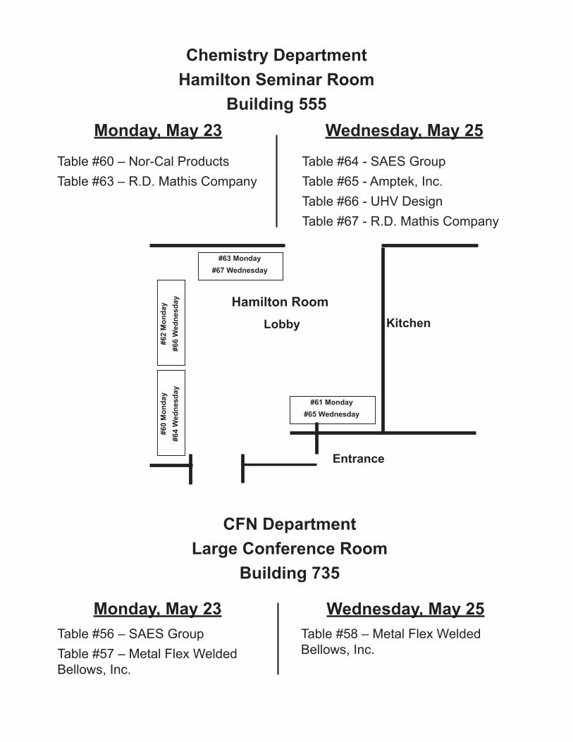
Chemistry DepartmentHamilton Seminar Room
Building 555
Entrance
Hamilton RoomKitchenLobby
#63 Monday#67 Wednesday
#62
Mon
day
#66
Wed
nesd
ay#6
0 M
onda
y#6
4 W
edne
sday
#61 Monday#65 Wednesday
Monday, May 23
Table #60 – Nor-Cal ProductsTable #63 – R.D. Mathis Company
Wednesday, May 25
Table #64 - SAES GroupTable #65 - Amptek, Inc.Table #66 - UHV DesignTable #67 - R.D. Mathis Company
CFN DepartmentLarge Conference Room
Building 735
Monday, May 23Table #56 – SAES GroupTable #57 – Metal Flex Welded Bellows, Inc.
Wednesday, May 25Table #58 – Metal Flex Welded Bellows, Inc.
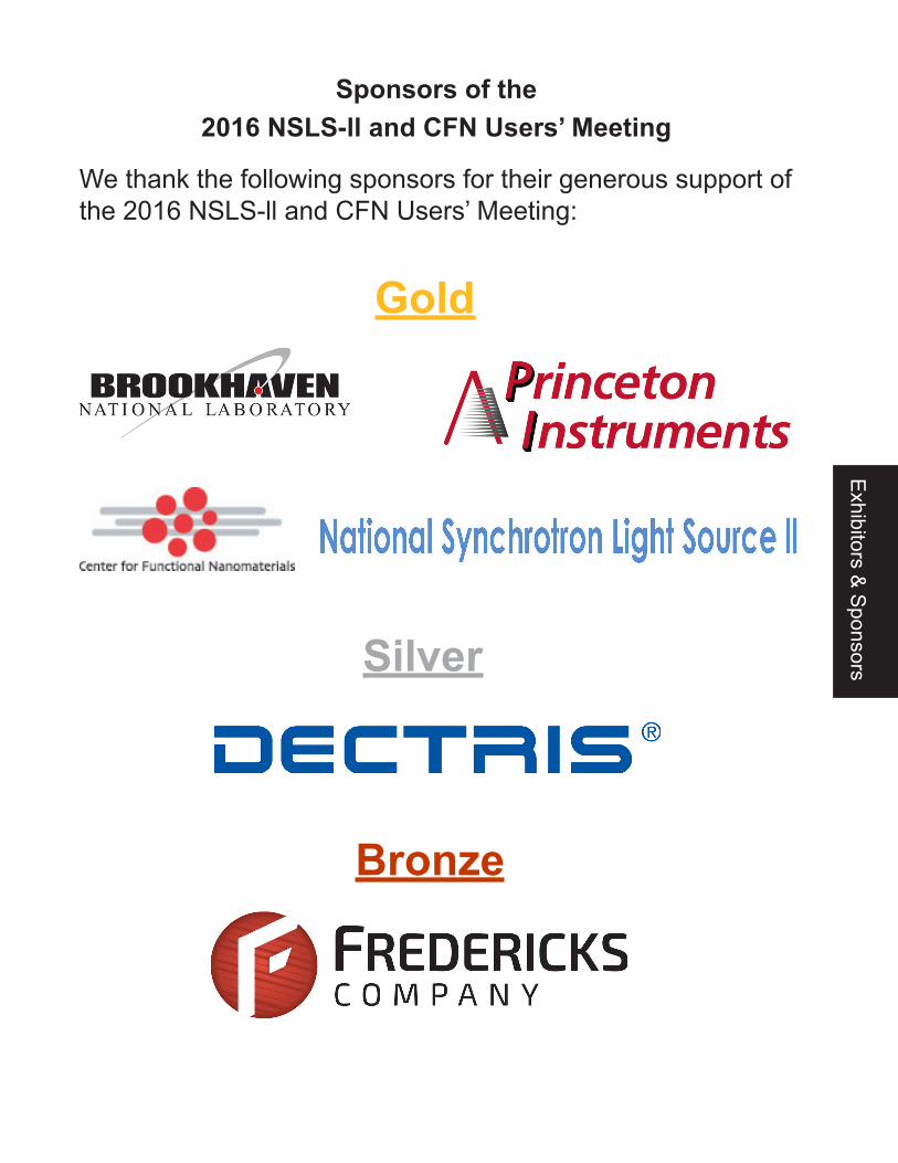
Exhibitors &
Sponsors
Sponsors of the2016 NSLS-ll and CFN Users’ Meeting
We thank the following sponsors for their generous support of the 2016 NSLS-ll and CFN Users’ Meeting:
Gold
Bronze
Silver

Exhibitor PresentationsBerkner Hall, Conference Room C
Time Exhibitor Presentation Title11:00 a.m. Dectris EIGER: high-speed
detectors enabling serial synchrotron crystallography
11:30 p.m. Applied Vacuum Technology
Speciality Materials for UHV Applications
12:00 p.m. Anderson Dahlen
Advanced Vacuum and Pressure Vessel Capabilities for Beamline Applications
1:30 p.m. XIA The FalconX, an ultra-high rate multi-channel digital signal processor for X-ray spectroscopy
In a special offering, several exhibitors will also be demonstrating their products on Tuesday, May 24 at mini-workshops in Berkner Hall. Please review the following schedule. We hope you can attend!

Exhibitors &
Sponsors
Equipment and Instrumentation ExhibitorsWe thank the following vendors for their generous support of the 2016 NSLS-ll and CFN Users’ Meeting and for exhibiting their state-of-the-art products during the Equipment & Instrumentation Exhibit.
Aerotech, Inc. Table 29 101 Zeta Drive Pittsburgh, PA 15238 412-963-7470 [email protected]
Aerotech manufactures motion control components and complete motion system solutions for light source applications including diffraction, tomography and crystallography. From goniometers to fully integrated electromechanical systems, Aerotech has the experience and expertise to design, build and test a system to your exact requirements. Aerotech incorporates our own electromechanical systems, advanced controls, software, electronics and data acquisition into a single platform that makes setup and operation faster and easier, and provides the highest performance available.
Agilent Technologies Table 32 121 Hartwell Avenue Lexington, MA 02421 516-375-4864 [email protected]
Agilent Technologies, Vacuum Division is a world leader in providing total vacuum solutions, offering primary, high and ultra-high vacuum pumps, vacuum gauges, valves and fittings, and leak detectors for all applications. Agilent offers unique expertise in applications, support, and system design to integrate these superior components into optimized vacuum solutions.
Amptek, Inc. Table 6514 DeAngelo Drive Bedford, Massachusetts 01730 781-333-7365 [email protected]
Amptek will be located in Bldg. 555, Chemistry, Hamilton Rm. on Wednesday, May 25 at the “New Detectors for New Light Sources” Workshop.Amptek is a high technology company and a recognized world leader in the design and manufacture of state-of-the-art nuclear instrumentation for the satellite, x-ray and gamma ray detection, laboratory, analytical, and portable instrumentation industries.Products include Si-PIN and SDD x-ray detectors, Digital Pulse Processors, and Gamma ray detectors and space mission products such as Space applications of Amptek’s products include hybrid preamplifiers and front-end electronics, plasma analyzers (ESA), and radiation monitors/dosimeters (CEASE)
Angstrom Scientific, Inc. Table 37 120 N. Central Ave., Suite 3 Ramsey, NJ 07446 201-962-7222 [email protected] Scientific Inc., provides nanotech and materials characterization solutions. Specifically: Kleindiek Nano-manipulators, Hitachi Tabletop-SEM/EDX, Mel-Build Analytical TEM holders, Deben Microscopy Accessories, Bionavis SPR, Jordan Valley XRD & Evactron Plasma Cleaners. Additionally, we buy and sell used electron microscopes and FIBs.

Applied Diamond, Inc. Table 413825 Lancaster Pike Wilmington, DE 19805 302-999-1132 [email protected]
Applied Diamond supplies products made from single crystal and polycrystalline diamond, including highly transparent windows, ultra high thermal conductivity high spreaders and thin targets for beamlines. We have expertise in diamond polishing for smooth surfaces, metallization for bonding and mounting of windows to flanges.
Applied Vacuum Technology/Anderson Dahlen Table 256850 Sunwood Dr NW Ramsey, MN 55303 952-442-7005 [email protected]
Applied Vacuum Technology designs and manufactures custom chambers, welded assemblies, flanges and precision components for high and ultra-high vacuum applications. AVT is a division of Anderson Dahlen Inc. With decades of experience in custom stainless steel fabrication, Anderson Dahlen’s capabilities for metal forming, machining, and welding are ideal for manufacturing large (20’ in length, 14’ in diameter) vacuum chambers. AVT/AD’s quality system is certified to ISO 9001:2008 and Nuclear Quality Assurance (NQA-1).
Art Robbins Instruments Table 521293 Mountain View Alviso Road, Suite D Sunnyvale, CA [email protected]
The scorpion is a high speed single channel pipettor capable of doing many liquid handling assays using varous sizes of pipetting tips.
attocube systems Inc. Table 112020 Stuart Street Berkeley, CA 94703 [email protected]
attocube is a worldwide supplier for ultra-high precision piezo positioning systems and multi-axes interferometric displacement sensors. The company offers piezodrive technology with extremely rugged yet cost efficient design and attocube’s patented and R&D100 award-winning fiber interferometer can be applied to multipurpose displacement measurements, as needed in extreme environmental positioning applications, coordinate measurement machines or micromachining applications.
AXILON AG Table 9 Emil-Hoffmann-Str. 55-59Koeln, 50996 Germany+49 (221) 16532400 [email protected]
AXILON is a strong new corporation serving the international synchrotron, accelerator & photon community. Based on the extensive and long-term experience of our dedicated experts, we serve our customers with excellent and efficient solutions for complete beamlines, beamline components, monochromators, mirror systems, experimental stations, X-ray microscopes, insertion devices and other special engineering and manufacturing solutions.
Exhibitors &
Sponsors
Canberra Table 40 800 Research Parkway Meriden, CT 06450 [email protected]
Canberra is the leading supplier of innovation and cost-effective nuclear measurement solutions and services used to maintain safety of personnel, assess the health of nuclear facilities and safeguard the public and the environment. Applications for Canberra offerings include health physics, nuclear power operations, Radiation Monitoring Systems (RMS), nuclear safeguards, nuclear waste management, environmental radiochemistry and other areas.
Carl Zeiss SMT GmbH Table 48Rudolf-Eber-Str. 2 Oberkochen, 73447 Germany +4973642005971 [email protected]
Carl Zeiss SMT is a reliable partner for the manufacturing of synchrotron mirrors. We implement powerful metrology and manufacturing techniques for the upcoming generation of highest-quality optical components for synchrotron radiation and other x-ray applications.
COSMOTEC, Inc. Table 21229 Polaris Ave. Suite 3Mountain View, CA [email protected]
Japan’s #1 Ceramic-to-Metal, hermetic sealing, electrical feedthroughs are now available in America.We work very closely with our clients, scientists, corporations, researchers, government labs, universities and individuals. Cosmotec respect the accomplishments or achievements with the people involved. We will amaze you with our custom manufacturing capabilities. Whether it is “one quantity” order, Cosmotec will work at its best to not let our clients down. We will “WORK TOGETHER” with our clients and find the best solution. Whether they are ceramic chambers, beam positioning monitors, (BPM), ceramic-to-metal bonding technology, we will provide solutions.
Duniway Stockroom Table 5 48501 Milmont DriveFreemont, CA 94538650-969-8811 [email protected]
For 40 years, Duniway Stockroom has supplied new and used vacuum equipment to Universities, government laboratories, OEM’s, Fortune 500 corporations and smaller end-users around the world.Duniway Stockroom specializes in vacuum equipment and supplies; ion pumps and controls; flanges, gaskets, bolts and nuts; vacuum gauges and controls; mechanical pumps and rebuild kits; supplies (oils, greases, hoses, bell jars) diffusion pumps and leak detectors. Vacuum pump (diffusion, turbomolecular, mechanical and ion) rebuilding services and a variety of reconditioned equipment.
Edwards Vacuum, Inc. Table 506416 Inducon Corporate Drive Sanborn, NY 14132800-848-9800 [email protected]
Edwards is a leading developer and manufacturer of sophisticated vacuum pumps, vacuum system products, abatement solutions and related value-added services. Our products are used for analytical instruments, a wide range of R&D applications and are integral in the manufacturing processes for semiconductors, flat panel displays, LEDs and solar cells. Edwards’ products are used within a diverse range of applications including power, glass and other coating applications, steel and other metallurgy, pharmaceutical and chemical processes.
FMB Oxford Table 51Unit 1-4 Ferry Mills Osney Mead Oxford OX2 0ES [email protected]
Joining forces in 2007, FMB Berlin & FMB Oxford have become established leaders in the supply of Synchrotron beamline components and systems. The combined business has the largest installed base and greatest range of products in the synchrotron community and has the design capability and manufacturing capacity to handle any beamline requirements, from the smallest component to multiple beamlines.
Gamma Vacuum Table 7 2915 133rd Street WestSuite 101B Shakopee, MN [email protected]
Gamma Vacuum designs, manufactures, and services ion pumps, titanium sublimation pumps, and their controls.We have grown to be an industry leading ion pump supplier through superior quality, delivery, service and innovation. The employees of Gamma Vacuum have experience in real world vacuum applications ranging from systems manufacturing and optics assembly to TIG welding for vacuum environments.Our staff and facility are dedicated to one thing; creating the purest vacuum environments on earth.
GNB Corporation Table 33 3200 Dwight Road, Ste. 100Elk Grove, CA [email protected]
GNB has an over 40 year proven track record of manufacturing high quality, custom engineered vacuum solutions for the scientific, industrial, and research vacuum industry. As America’s leading manufacturer of large vacuum chambers and valves, we also deliver a diverse range of high vacuum, and high temperature, products and services.
Exhibitors &
Sponsors
Goodfellow Corporation Table 46 125 Hookstown Grade RoadCoraopolis, PA [email protected]
Goodfellow supplies pure metals, alloys, ceramics, polymers and composites as discs, sheets, foils, films, lump, powder, rods, wires, tubes, etc. to the research (R&D) and industrial markets. We serve the research, development and prototyping markets by offering small quantities of material from a stock of over 47,000 catalog items which are available for shipping worldwide in under 48 hours. We also offer larger quantities of material to the industrial production market. In both cases, we can also supply materials to your individual specification, as required.
Hiden Analytical Inc. Table 2 37699 Schoolcraft RoadLivonia, MI [email protected]
Hiden Analytical manufactures an extensive range of high performance quadrupole mass spectrometers for plasma characterization studies, surface science applications, precision gas analysis and vacuum diagnostics. For demanding UHV applications our range of precision residual gas analyzers feature gold plated ion sources for minimal source outgassing and electron stimulated desorption. All systems include our Threshold Ionization Mass Spectrometry capability for enhanced spectral deconvolution. For additional information visit us on the web at www.HidenInc.com
Huber Diffraction Table 558344 West Ave C4Lancaster, CA [email protected]
Huber Diffraction designs and manufactures high-precision positioning systems primarily used for X-ray diffraction in laboratories and at synchrotron beam sources. Other application fields are diffraction experiments with neutrons, laser technology, astronomy and precise measurement technology.
Inprentus Table 47 60 Hazelwood Drive Champaign, IL 61820 217-239-9862 [email protected]
Inprentus provides custom mechanically ruled, high-efficiency variable line spacing diffraction gratings for EUV and soft x-ray use, manufactured using a new process developed at the University of Illinois at Urbana-Champaign. Inprentus currently manufactures gratings with the following specifications: Up to 20,000 resolving power; Blaze angles between 1 degree and 5 degrees; 300-2500 lines per mm; Size 220mm long x 50mm wide Inprentus was founded in 2012 by Prof. Peter Abbamonte - a physics professor at the University of Illinois at Urbana-Champaign, who has developed or co-developed many facilities at x-ray light sources, most recently the IEX-CDT soft x-ray project at the Advanced Photon Source.

InSync, Inc. Table 1 2511C Broadbent Pkwy Albuquerque, NM 87107 505-345-2660 [email protected]
An optical manufacturing company. Specialty is “state of the art” polishing up to 1500mm in size. Capabilities; Computer Design, Finite Element Analysis, Slicing, Grinding, Machining, Etching, Bonding, Lapping, Polishing, Coating, Metrology. Shapes; Cylindrical, Spherical, Flat. Designs; Internally Cooled, Rectangular, Round. Materials; Silicon, Glass, Metals. JJ X-ray A/S Table 45 Diplomvej 377Syngby 2800 [email protected]
JJ X-RAY is a Danish company that develops, designs and produces highly specialized components and assemblies for scientific x-ray, synchrotron radiation and neutron instrumentation.We are widely known for our high precision and durable JJ X-Ray slits and collimators. Our standard component portfolio is constantly expanding.
Johnsen Ultravac A Division of JMC Table 39 3470 MainwayBurlington, Ontario L7M 1A8Canada [email protected]
Johnsen Ultravac offers a wide range of Front Ends and Beamline components for an array of different applications.
Kaman Industrial Technologies Table 49 18 Commerce DriveHauppauge, NY [email protected]
Your one stop source for All thing Automation. If it moves, makes it move, makes it stop, we can help.
Kashiyama Table 28 41432 Christy StreetFremont, CA [email protected]
KASHIYAMA is a Dry Screw Pump Innovator who can provide wide range of durable and reliable dry pumps for the high-tech and scientific communities . Over 30 years experience in the vacuum pump business allows us to develop and supply high quality equipment tailored to customers’ requirements, which has contributed a huge role in different industries.We offer: 1. Dry Vacuum Pump: Advanced Screw design with anti corrosion material, Maximum MTBF under harsh process, Superior energy savings, Minimum cost of ownership, Wide range of line up ( range from 110 l/min to 200,000 l/min)2. Best Service: World Wide Support, Fast response and guaranteed work, Quick field service and quotes available in most locations
Exhibitors &
Sponsors
Key High Vacuum Products, Inc. Table 15 36 Southern Blvd.Nesconset, NY 11767 [email protected]
Key High Vacuum Products, Inc. has been designing and manufacturing vacuum components since 1976. We are a complete vacuum component manufacturer. Piezoelectric valves, Gas Diffusers, Controllers, Stainless Steel valves, Butterfly valves, ISO-KF building block components, and our offerings keep growing. Our model shop is equipped to handle custom fabricated components and systems. Please feel free to contact us; we look forward to hearing from you.
Kurt J. Lesker Company/UHV Design Ltd. Table 16 1925 Route 51Jefferson Hills, PA 15025 [email protected]
Kurt J. Lesker Company® is partnered with UHV Design (www.uhvdesign.com), a well-established supplier of precision synchrotron manipulation. Products include linear actuators for beam line diagnostics along with end station manipulators, such as multi-axis sample stages, sample transfer tools and telescopic distribution manipulators. Customized products are also offered at competitive prices through in-house design and manufacturing. The synchrotron products are offered alongside the KJLC®’s extensive range of vacuum components, chambers, and deposition systems. Lake Shore Cryotronics, Inc Table 34575 McCorkle BoulevardWesterville, OH 43082 [email protected]
Supporting advanced research since 1968, Lake Shore is a leading innovator in measurement and control solutions under extreme temperature and magnetic conditions. Products include cryogenic temperature sensors and instrumentation, magnetic test and measurement systems, probe stations for electronic/magnetic material testing, and precision materials characterizations systems for exploring electronic and magnetic properties. Lake Shore serves an international base of scientists at leading university, government, and commercial research institutions and is supported by a global sales network.
MDC Vacuum Products, LLC Table 19 23842 Cabot Blvd. Hayward, CA 94545 510-265-3500 [email protected]
MDC Vacuum Products LLC along with our Insulator Seal Division (ISI) is a world leading supplier of vacuum components and ceramic to metal seals offered at competitive prices. Both MDC and ISI offer thousands of off the shelf products or have the capability of providing custom engineered solutions to meet your exact requirements.Please visit our website and have a look or give us a call and discuss your application needs with one of our knowledgeable staff.
Metal Flex Welded Bellows, Inc. Tables 57 & 58149 Lakemont Rd. Newport, VT 05855802-334-5550 [email protected]
Metal Flex®, will be located in Bldg. 735, CFN, in front of the large conference room on Monday, May 23 at the “Two-Dimensional van der Waals Semiconductors for Energy Conversion Applications” Workshop.Metal Flex®, will be located in Bldg. 735, CFN, in front of the large conference room on Wednesday, May 25 at the “Renewable Energies: Where Applied and Basic Sciences Meet” and “The Earth Laboratory: Experimental and Computational Tools and Infrastructure for Cross-cutting Earth Sciences” Workshops.Metal Flex®, in existence since 1981, is known throughout the world as a leader in welded bellows technology. Our products are used in semiconductor, aerospace/aircraft, Ultra-High Vacuum (UHV), and many other research, industrial and commercial applications. Metal Flex® performs design, manufacturing, and testing activities in house, which allows us to react quickly and precisely to your changing needs. We welcome the opportunity to assist you with your most demanding requirements and look forward to providing you with a solution that meets and exceeds your needs.
MICRONIX USA, LLC Table 1815375 Barranca Pkwy.E-106 Irvine, CA 92618 949-480-0538 [email protected]
MICRONIX USA supplies micro- and nano-positioning equipment with a focus on the research market. We offer a full range of precision positioners, hexapods, and control electronics, as well as complete system integration services. Additionally, MICRONIX USA is known as the premier supplier for vacuum to 10-9 torr, clean room, and extreme temperature applications. MICRONIX USA is the exclusive U.S. distributor for Symetrie high-precision hexapods.
Molmex Scientific Inc. Table 27518 Pleasant StreetNorthampton, MA [email protected]
Molmex Scientific Inc is the North American distributor for Dectris hybrid pixel detectors and SAXSLAB Small Angle X-ray Scattering (SAXS) end stations, with multiple and moving detectors in vacuum. This is an excellent platform for both Materials Science and Protein Solution Scattering, featuring our pipetting solution robotics and optical sample positioning feedback.
Morrell Instruments Table 20502 Walt Whitman RoadMelville, NY [email protected]
Morrell Instrument Company has served the BNL scientific community for the past 38 Years. It has been our primary objective to give our clients the best possible pre and post-sale support. To do this we have assembled a highly trained staff that shares this philosophy.In addition to Nikon, we are authorized distributors for well over 100 other manufacturers, including JOEL’s exciting new Neoscope bench-top SEM. We test all equipment and choose only the highest quality products. We stand by every product we distribute. Please give us the opportunity to prove ourselves, we will not let you down.
Exhibitors &
Sponsors
Newport Corporation Table 171791 Deere Avenue Irvine, CA 92606 800-222-6440 [email protected]
Newport Corporation (NASDAQ: NEWP) is a leading global supplier of advanced technology products and solutions for Scientific Research, Life & Health Science, Aerospace & Defense, Photovoltaics, Industrial Manufacturing, Semiconductors, and Microelectronics markets. Established in 1969, Newport has over 40 years of industry knowledge and expertise across a broad range of technologies allowing the company to continually deliver innovative products in the areas lasers, photonics instrumentation, sub-micron positioning systems, vibration isolation, optical components and subsystems and precision automation to enhance the capabilities and productivity of its customers’ manufacturing, engineering and research applications. In Addition, Newport has built a strong history of partnering with OEM customers delivering solutions from sub assemblies to full solutions including design, testing and manufacturing.
Nor-Cal Products Table 60 (Bldg. 555)3030 Laura Lane, Suite 100 Middleton, WI 53562 [email protected]
Nor-Cal Products will be located in Bldg. 555, Chemistry, Hamilton Rm. on Monday, May 23 at the “Operando Structural Characterization of Polymer Processing” Workshop.Nor-Cal Products has specialized in highly configured custom chambers, manifolds, baseplates, valves, and traps for over 40 years. Exceptional global support. Expert in-house engineering, precision welding and fabrication, CMM measurement, surface treatments, electropolish, chem clean, XRF and RGA analysis, Class 1000 clean rooms. Over 6000 competitively priced standard components. Complete system and subassembly integrations. ISO 9001-2008 and ASME U Stamp certified. 3D Models on-line.
Oerlikon Leybold Vacuum Table 125700 Mellon Road Export, PA 15632 [email protected]
Oerlikon Leybold Vacuum is a world leading supplier of high and ultra-high vacuum equipment for the Analytical, R&D and Scientific instrument market. Products include turbomolecular pumps with conventional ceramic and magnetic bearing technology, rotary vane pumps, scroll pumps, vacuum gauges and leak detectors. OLV also manufactures a turn-key UHV general purpose experimentation tool and the UNIVEX high vacuum deposition system for RF/DC sputtering, Ebeam, thermal evaporation and/or ion assisted deposition.
OMS Motion, Pro-Dex Table 1315201 NW Trakehner WayPortland, OR [email protected]
OMS Motion, a Pro-Dex company, provides world-class motion control solutions for semiconductor & medical equipment, life sciences as well as research institutions around the world. Ethernet, USB, PCI, etc., up to 10-axes per controller. New products include integrated drives & controls. OMS provides 30+ years of experience, proven reliability and service that is trusted worldwide.
Oxford Instruments Table 35300 Baker AvenueSuite 150Concord, MA [email protected]
Oxford Instruments NanoScience designs, supplies and supports market-leading research tools that enable quantum technologies, new materials and device development in the physical sciences. Our tools support research down to the atomic scale through creation of high performance, cryogen free low temperature and magnetic environments, based upon our core technologies in low and ultra low temperatures, high magnetic fields and system integration, with ever-increasing levels of experimental and measurement readiness. Oxford Instruments NanoScience is a part of the Oxford Instruments plc group.
Pascal Technologies, Inc. Table 8 11903 Bowman DriveSuite 101B Frederickburg, VA 22408 540-809-6932 [email protected]
Pascal Technologies is an all-in-one solution for your vacuum systems and vacuum equipment needs. We offer everything from UHV ion pumps, cryopumps, and chambers, to vacuum measurement, sample transfer, and leak detection solutions. Please visit our website for additional information: www.pascaltechnologies.com.
Pfeiffer Vacuum Table 3824 Trafalgar Square Nashua, NH 03063 [email protected]
Pfeiffer Vacuum provides vacuum solutions from a single source. In addition to a full range of hybrid and magnetically levitated turbo pumps, our portfolio includes backing pumps, measurement and analysis devices, components as well as vacuum chambers and systems. For over 125 years, Pfeiffer Vacuum has stood for innovative solutions and high-tech products that are used in the Analytics, Industry, Research & Development, Coating and Semiconductor markets.
PI (Physik Instrumente) Table 1416 Albert Street Auburn, MA [email protected]
PI is a leading manufacturer of precision motion control equipment, piezo motors, air bearing stages and hexapod parallel-kinematics for semiconductor applications, photonics, bio-nano-technology and medical engineering. PI has been developing and manufacturing standard & custom precision products with piezoceramic and electromagnetic drives for 4 decades. The company has been ISO 9001 certified since 1994 and provides innovative, high-quality solutions for OEM and research. PI is present worldwide with eleven subsidiaries, R&D / engineering on 3 continents and total staff of 800+.
Princeton Instruments Table 36 3660 Quakerbridge Road Trenton, NJ 08619 [email protected]
Princeton Instruments provides high-performance CCD, ICCD, and EMCCD cameras and spectrographs including X-ray imaging and spectroscopy systems. Systems can be very easily optimized with custom
Exhibitors &
Sponsors
phosphors for X-ray diffraction, micro-computer tomography, streak tube readout and other applications. Direct detection systems used for coherent X-ray imaging, X-ray holography and soft X-ray diffraction are also provided. Products include new SOPHIA CCD cameras, IsoPlane aberration-reduced spectrographs and PI-MAX4 ICCD cameras, and NIRvana InGaAs cameras for NIR/SWIR applications.
Quantum Detectors Table 53 R104, RALFermi AvenueHarwell Oxford, Oxfordshire, OX11 [email protected]
Quantum Detectors develop novel detectors for synchrotron beamlines. We specialise in high rate instrumentation, but also that offering high energy sensitivity and spectroscopic area detectors. Come along to the booth to meet us and our new technology!
Queensgate Instruments (A Brand of Elektron Technology UK Ltd) Table 31 Broers BuildingJJ Thomson AvenueCambridge, Cambridgeshire CB3 0FA GBR+44 (0)1223 37 [email protected]
Queensgate Instruments, an Elektron Technology brand, specialise in creating nanopostioning and sensing solutions for high technology industries with variants suitable for precision measurement in UVAC, radiation environments and cryogenic temperatures. We specialise in creating tailored offerings to challenging problems, advise on the best use of standard products through to end to end delivery of custom components and systems. Our range includes: Closed loop Piezo-actuated stages; Actuators/Translators; Electronic Control Mechanisms; NanoSensorsFurther information: http://www.nanopositioning.com/Contact: [email protected]
R.D. Mathis Company Tables 63 and 67 (Bldg. 555)2840 Gundry Avenue Signal Hill, CA 90755 [email protected]
R. D. Mathis Company will be located in Bldg. 555, Chemistry, Hamilton Rm. on Monday, May 23 at the “Operando Structural Characterization of Polymer Processing” Workshop.
R.D. Mathis Company will be located in Bldg. 555, Chemistry, Hamilton Rm. on Wednesday, May 25 at the “New Detectors for New Light Sources” Workshop.
The R. D. Mathis Company specializes in the fabrication of high vacuum evaporation sources and materials for the thin film coating and metallizing industries. We offer a comprehensive selection of Tungsten, Molybdenum and Tantalum sources as well as custom fabrication to meet your specific coating needs. High Purity evaporation materials such as gold, silver, nickel, aluminum, etc. are also available in a variety of purities and sizes. On display will be a wide selection of our standard evaporation sources and a variety of evaporation materials. Please stop by and say hi. ISO9001 / AS9100 Certified. www.rdmathis.com

RI Research Instruments Table 30Friedrich-Ebert-Strasse 75 Bergisch Gladbach [email protected]
From Accel to RI Research Instruments. Our name stands for innovative solutions and high performance through many years of experience. At RI we develop, design, manufacture and test high performance accelerator and photon instrumentation components and systems to the requirements of our customers in research and industry. Our Photon Instrumentation product portfolio includes beamline systems, monochromators (step and fast scanning), mirror systems, front end components, insertion devices, endstations, and LN2 cryocoolers.
Rigaku Innovative Technologies, Inc. Table 31900 Taylor Road Auburn Hills, MI 48326 [email protected]
With 30+ years producing Multilayer X-ray Optics, Rigaku Innovative Technologies introduced many new optics and instruments for synchrotrons. Rigaku/Osmic designs and builds innovative instruments, multilayer coatings and advanced focusing monochromators for beamlines and endstations, including our new 2-D Kratky SAXS camera. Now refurbishing used optics! Regain your investment in the expensive optical substrate. Capabilities include multiple-stripe DMMs, graded d-spacings and picometer precise coatings on complex optics to 1200mm. High precision Johansson crystals now available.
SAES Group Table 56 (Bldg. 735 - Monday)1122 E. Cheyenne Mountain Blvd. Table 64 (Bldg. 555 - Wednesday) Colorado Springs, CO 80906 [email protected]
SAES Group will be located in Bldg. 735, CFN, in front of the large conference room on Monday, May 23 at the “Two-Dimensional van der Waals Semiconductors for Energy Conversion Applications” Workshop.SAES will be located in Bldg. 555, Chemistry, Hamilton Rm. on Wednesday, May 25 at the “New Detectors for New Light Sources” Workshop.SAES® Group is the world leader in a variety of scientific and industrial applications where stringent vacuum conditions are required. For more than 70 years, the NEG technology has provided optimal performance for ultrahigh vacuum and high vacuum systems. Because of the small size and high performance, NEG pumps are widely used in mass spectrometry requiring high performance in a lightweight low volume package. Since these pumps do not always require continuous power, it makes it ideal for portable mass spectrometers, requiring constant pumping during transportation or continued pumping during power failures. Visit our booth to see our expanded line of pumps!
SmartAct Inc. Table 222140 Shattuck Avenue STE 1103 Berkeley, CA 94704 415-373-2283 [email protected]
SmarAct offers sophisticated products for micro- and nanopositioning. Our products ranges from positioners, advanced control systems to end effectors and tools for the micro- and nanoworld. The piezo-based positioners are offered with a scaleable control systems so that they are just as suitable for simple operations as for complex automations. We offer miniaturised robotic systems and parallel kinematics that are capable of very precise tasks and which can be tailored to meet your exact requirements.

Exhibitors &
Sponsors
SPECS Surface Nano Analysis, Inc. Table 2320 Cabot Blvd., Suite 300Mansfield, MA 02048 [email protected]
SPECS manufactures cutting-edge systems and components for surface analysis in UHV, based on methods like XPS, UPS, AES, ISS, STM, LEEM/PEEM, LEED, SIMS, SNMS and HREELS. We offer a variety of sources for deposition, excitation and charge neutralization as well as analyzers, monochromators and research microscopes like LEEM and STM. A strong focus of our work is on customized systems combining thin film preparation (MBE) with spectroscopic and microscopic options.
Starrett Tru-Stone Techologies Table 441101 Prosper DriveWaite Park, MN 56387 800-959-0517 [email protected]
Starrett Tru-Stone Technologies specializes in precision granite machine bases & assemblies. We partner with you to add expertise in design collaboration, high-quality on-time manufacturing and complex assembly for your precision base. In addition to granite bases, Tru-Stone techs install precision rails, air mounts, brackets, pneumatic systems and cabling. Custom stands are also provided. Materials beyond granite include ceramic, carbon fiber materials.
Strumenti Scientific Cinel SRL Table 4 Via Dell’Artigianato 14-14AVigonza Padova35010 Italy+39 049 [email protected]
Founded in 1979, Strumenti Scientifici CINEL (http://www.cinel.com/) is an established supplier of components and integrated systems for synchrotron, XFEL light sources and particle accelerators. We provide innovative and tailored solutions into integrated UHV systems, complete beamlines, beamline components (mirror systems, monochromators, etc.). Our combination of in-house expertise in precision design and engineering, metrology, assembly and integration, vacuum and, last but not least, our precision manufacturing capabilities allowing us to produce every single part of our instruments, make Strumenti Scientifici CINEL the partner of choice to realize challenging and state-of-the-art instruments for your beamlines.
Sydor Instruments Table 43291 Millstead Way Rochester, NY 14624 [email protected]
See Sydor Instrument’s new detection and monitoring products for Synchrotron applications including beam position & flux monitors, silicon strip detectors, and direct detection CCD cameras. We also offer a suite of streak cameras, fast high voltage pulse electronics, and photoemissive detectors. Sydor has a history of developing and commercializing next generation detection technology and specializes in custom diagnostics, custom integration and technology transfer. Need a custom diagnostic? Have a technology ready for transfer? Talk to Sydor today.
Toyama Co. Ltd. Table 63816-1 Kishi Yamakita-machi Ashigarakami-gun,Kanagawa 252-0003 JPN +81462531411 [email protected]
Toyama is fundamentally an engineering company, manufacturing ultra-precision systems for experimentation at the cutting edge of science. If you have a new concept that needs to be developed, then Toyama is the place to come. We have the technology and experience to turn your ideas into reality. Our long history of supplying scientific instrumentation means that we have a wide range of standard products which can, if required, be customised to meet new technical challenges.
UHV Design Table 66 (Bldg. 555)Lewes Road Laughton, East Sussex BN6 8BN GBR +49 3641 4275-0 [email protected]
UHV Design will be located in Bldg. 555, Chemistry, in front of the Hamilton room on Wednesday, May 25 at the “New Detectors for New Light Sources” Workshop.UHV Design - specialists in UHV motion and manipulation products for beamline diagnostics and end-stations.
Vacuum Solutions Group Tables 24 and 26PO Box 2136Teaneck, NJ 07666 [email protected]
Vacuum Solutions Group represents MPF, ColdEdge, Osaka Vacuum, Mewasa, and HVA Vacuum Valves.
VAT, Inc. Table 10 500 West Cummings ParkSte 5450Woburn, MA 01801 [email protected]
VAT has been the global leader in vacuum valves for 50+ years. Visit with our team members to learn about VAT expertise in focus areas including valves, bellows, integrated solutions, service and much more! VAT capabilities and strength are founded in vacuum technology and quality, both of which are the driving forces behind VAT innoVATion.
XIA LLC Table 42 31057 Genstar Rd. Hayward, CA 94544 510-401-5760 [email protected]
XIA LLC invents, develops and markets advanced digital data acquisition and signal processing electronics for x-ray and gamma-ray detector applications in university research, national laboratories and industry. We are technology leaders in multi-channel, high-rate and high-resolution spectroscopy systems, with a history of collaborative research with national labs and universities. We currently manufacture and sell about a dozen instruments in 4 product families.

Exhibitors &
Sponsors
AccommodationsAccommodations on the BNL Site
Reservations: Housing is very limited. Space is assigned on a first-come, first-served basis. For rates and availability, please contact the Housing Office at (631) 344-2541 or [email protected].
Housing charges must be paid to the Housing Receptionist on arrival.
Check-Out time is 3:00 p.m. Before leaving, return your keys to the Housing Office.
The Housing Office is open Monday through Friday, 8:00 a.m. to 10 p.m., and also on Sunday from 4 p.m. to 10 p.m. Those arriving or leaving at other times may pick up or drop off keys at Police Headquarters, Building 50.
Accommodations Offsite (*Roundtrip shuttle service will be provided to BNL from the hotels)
East Wind Long Island (This year’s Meeting Banquet will be held at the East Wind) Special Users’ Meeting / BNL Rate - $112.00 - includes a breakfast voucher to Myra’s Cafe, free high speed wireless internet, indoor swimming pool and 24 hour gym.free shuttle service to and from BNL. Upon check-in, please be sure to inform the front desk that you will be requiring the shuttle service to/from BNL.
5720 Route 25AWading River, NY 11792(631) 846-2337Exit 68 off the LIE Est. Travel Time:19 minutes 10.5 Miles from BNL. Estimated Travel Time from Long Island MacArthur Airport to East Wind: 36 mins / 27.1 miles.The special room rate will be available until May 6, 2016.
Ramada Plaza Long Island Special Conference / BNL Rate - $126.00 plus tax - includes free hot buffet breakfast, free high speed wireless internet, fitness center, free shuttle service to LI Islip Airport and Ronkonkoma Train Station and morning and afternoon shuttle service to and from BNL. Upon check-in, please be sure to inform the front desk that you will be requiring the shuttle service to/from BNL.
1730 North Ocean Avenue Holtsville, NY 11742 (631) 758-2900 Exit 63 off Long Island Expressway (LIE)Est. Travel Time:16 minutes 10.3 Miles from BNLThe special room rate will be available until May 1, 2016.
SpringHill Suites by MarriottSpecial Users’ Meeting / BNL Rate - $126.00 - King Studio - includes free hot buffet breakfast, free high speed wireless internet, fitness center, indoor pool. Upon check-in, please be sure to inform the front desk that you will be requiring the shuttle service to/from BNL.
2 Sawgrass Drive Bellport, NY 11713(631) 924-0090Estimated Travel Time:13 mins/7.93 miles from BNLEstimated Travel Time from Long Island MacArthur Airport to SpringHill Suites: 16 mins / 10.32 miles.The special room rate will be available until May 6, 2016.
Hyatt Place Long Island East End Special Users’ Meeting / BNL Rate - $126.00 - includes free continental breakfast, free high speed wireless internet, fitness center. Upon check-in, please be sure to inform the front desk that you will be requiring the shuttle service to/from BNL.
451 E. Main StreetRiverhead, NY 11901631-208-0002Estimated travel Time:15 minutes 10.5 Miles from BNL
The special room rate will be available until April 17, 2016.

Offsite TransportationTrains
The Long Island Railroad serves all of Long Island with service to New York City’s Penn Station; connections are available from there to Amtrak and regional lines.
The closest Long Island Railroad Station to BNL is in Mastic/Shirley; however, trains arrive and depart more frequently at Patchogue and Ronkonkoma. To find schedules and more information, call (516) 822-5477, or visit the World Wide Web site: http://www.mta.nyc.ny.us/lirr/index.html
To get to the Mastic/Shirley LIRR station, take William Floyd (Rte. 46) south of the Lab, past the LIE, Route 27 and Montauk Highway. The parking lot is on the left just after the railroad tracks.
To get to the LIRR Ronkonkoma station, take the LIE to Exit 60, go south, and follow the signs. Parking here is sometimes scarce on weekdays, but the trains run early every hour and the trip takes only an hour and a half. Or, take the Lab car service.
The Port Jefferson station has fewer trains that take more time than Ronkonkoma trains, but the station is closer to the Lab than Ronkonkoma. Take Rte. 46 north to its end at Rte. 25A, following it for 15 miles and taking the right fork toward Port Jeff. At the T intersection, take a right; the station is on the south side of the tracks on the right side of the road. Passengers from Port Jeff need to change trains once (get off, stand at the same platform, get on the next train) to get to Manhattan.
Laboratory Cars/Train Shuttle
The BNL Transportation Office, Bldg.400A, ext. 2535, provides transportation to meet the Long Island Railroad (LIRR) train from New York City arriving in Ronkonkoma at 8:59 a.m., Monday through Friday, and also to catch the LIRR train to New York City leaving Ronkonkoma at 4:46 p.m., Monday through Friday. Due to limited seating, reservations are required for this service. Please telephone ext. 2535, email [email protected] or go to Bldg. 400A.
TaxisColonial Taxi (631) 589-7878Courtesy Taxi (631) 395-5237Four Ones Taxi Service (631) 281-8581Lindy’s Taxi (631) 654-3456Sunset Taxi (631) 588-8844
Rental CarsAlamo (800) 327-9633Avis (800) 331-1212Budget (800) 527-0700Dollar (800) 800-4000Enterprise (800) 325-8007 ~ onsite at BNL!Hertz (800) 654-3131National (800) CAR-RENTRent-A-Wreck (800) 535-1391Thrifty (800) 367-2277

Am
enities
Airport Limousine Services A-VIP Luxury Limousines (631) 655-5694Chris Dee Limousines (631) 979-3824 Crestwood Limousine (631) 399-5196, Cell (516) 457-6124 Dynamic Limousines (631) 291-6290 Elegant Limousine (631) 345-5541 Executive Limo (631) 696-8000 LI Limo (631) 234-8400 Tran-Star Executive (800) 894-7827 Winston (631) 924-1200
Onsite TransportationOn-Site Shuttle Bus
The On-Site Brookhaven Lab Courtesy Van offers on-call, door-to-door service between the hours of 8:30 a.m. and 4:15 p.m., Monday through Friday, excluding holidays. Please call extension 2714 for pickup. Please be prepared to give the following information: name; telephone extension; location of pickup; location of drop-off; and number of passengers.
Requests are accepted on a first-come, first-served basis. Be prepared to meet the van at the main entrance of your building. In order for us to be able to serve as many customers as possible, please be ready to board the van before making the call for pickup. Pick-ups can be arranged by calling ext. 2714 and providing your name, telephone extension, location of pickup, location of drop-off and number of passengers.
Computers, Phones & MessagesComputer terminals are located in Berkner Hall for use in logging on to your own computer or accessing your email during the meeting.
Messages can be left for you at the Conference Desk. The telephone number (during the meeting only) is (631) 344-3548. Messages will be posted on a bulletin board in front of Room D (Conference Desk).
A fax machine is located in Berkner Hall for those who require faxing services. The phone number is (631) 344-2069. See the Conference Desk for assistance in using the fax machine.

Nominees for the 2016-18NSLS-ll Users’ Executive Committee
Noel BlackburnOEP-BNLUpton, NY
Noel Blackburn is the Manager for University Relations and DOE Internship Programs in the Office of Educational Programs (OEP) at Brookhaven National Laboratory (BNL). Noel is responsible for designing, implementing and managing workforce development research programs for undergraduates, graduates, and faculty at BNL, while creating access opportunities for underrepresented groups into BNL and the DOE enterprise with such programs as the Interdisciplinary Consortium for Research and Educational Access in Science and Engineering (INCREASE). Before his present position, Blackburn was a Project Engineer on remediation projects for BNL’s Environmental Management Directorate and served in various engineering positions on local, regional and international civil engineering projects. Noel is truly concern in creating access to NSLS II for non-traditional users here in the U.S. and developing partnerships with countries in Latin America and the Caribbean.
Jen BohonCase Western Reserve University
Cleveland, OH
Jen Bohon is an Assistant Professor in the Case Western Reserve University Center for Synchrotron Biosciences and the lead beamline scientist for the NSLS-II XFP beamline (17-BM) currently under construction. This beamline is focused on in vitro and in vivo studies of structure and dynamics of biological macromolecules and is the first of the “partner” portfolio beamlines expected to come online at NSLS-II. In addition to biological research, Jen is involved in development of instrumentation for x-ray beamlines, including beam diagnostics for several NSLS-II beamlines. She has a long history of service to the synchrotron user community, having served on the UEC since 2009 (chair 2012). She is currently serving as the Outreach Officer for the NSLS-II UEC, and is a member of the National User Facility Organization (NUFO) steering committee. Jen has participated in numerous outreach and educational events on behalf of NSLS users to congressional representatives and is a strong advocate for synchrotron science.
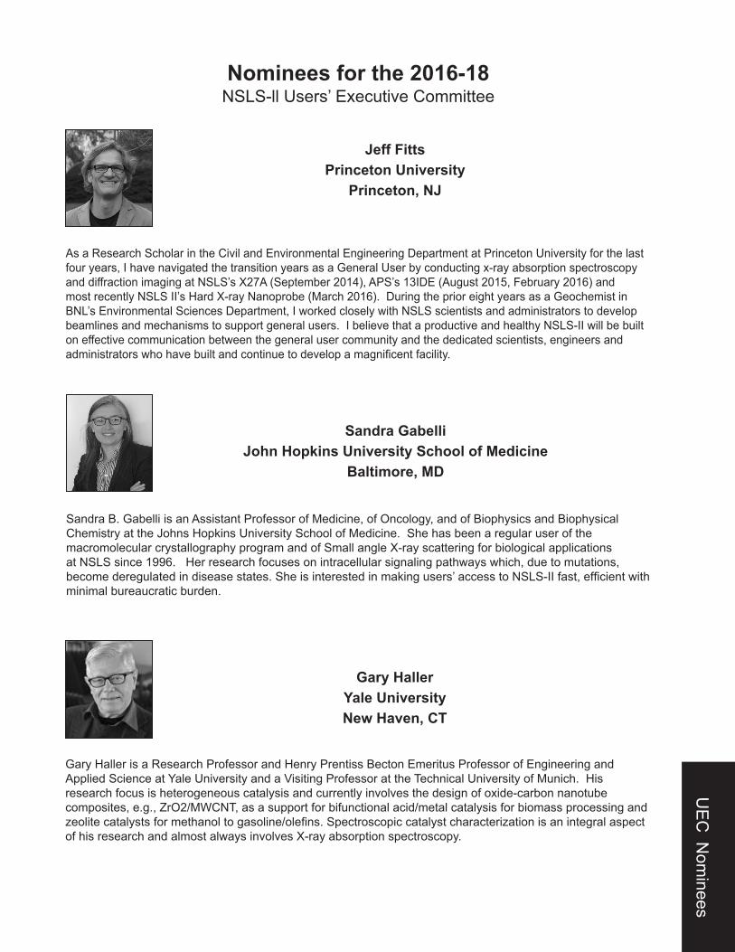
UE
C N
ominees
Nominees for the 2016-18NSLS-ll Users’ Executive Committee
As a Research Scholar in the Civil and Environmental Engineering Department at Princeton University for the last four years, I have navigated the transition years as a General User by conducting x-ray absorption spectroscopy and diffraction imaging at NSLS’s X27A (September 2014), APS’s 13IDE (August 2015, February 2016) and most recently NSLS II’s Hard X-ray Nanoprobe (March 2016). During the prior eight years as a Geochemist in BNL’s Environmental Sciences Department, I worked closely with NSLS scientists and administrators to develop beamlines and mechanisms to support general users. I believe that a productive and healthy NSLS-II will be built on effective communication between the general user community and the dedicated scientists, engineers and administrators who have built and continue to develop a magnificent facility.
Jeff FittsPrinceton University
Princeton, NJ
Sandra B. Gabelli is an Assistant Professor of Medicine, of Oncology, and of Biophysics and Biophysical Chemistry at the Johns Hopkins University School of Medicine. She has been a regular user of the macromolecular crystallography program and of Small angle X-ray scattering for biological applications at NSLS since 1996. Her research focuses on intracellular signaling pathways which, due to mutations, become deregulated in disease states. She is interested in making users’ access to NSLS-II fast, efficient with minimal bureaucratic burden.
Sandra GabelliJohn Hopkins University School of Medicine
Baltimore, MD
Gary Haller is a Research Professor and Henry Prentiss Becton Emeritus Professor of Engineering and Applied Science at Yale University and a Visiting Professor at the Technical University of Munich. His research focus is heterogeneous catalysis and currently involves the design of oxide-carbon nanotube composites, e.g., ZrO2/MWCNT, as a support for bifunctional acid/metal catalysis for biomass processing and zeolite catalysts for methanol to gasoline/olefins. Spectroscopic catalyst characterization is an integral aspect of his research and almost always involves X-ray absorption spectroscopy.
Gary HallerYale UniversityNew Haven, CT

Nominees for the 2016-18NSLS-ll Users’ Executive Committee
Shelly KellyHoneywell UOPDes Plaines, IL
Shelly Kelly is group leader of X-ray techniques and Modeling group at UOP LLC, A Honeywell Company. Her research is focused on understanding catalysis, molecular sieves and sorbents using X-ray synchrotron techniques with emphasis on X-ray absorption spectroscopy. She has participated as a lecturer in XAS workshops, reviewer of general user proposals, and as BAT member for the Inner Shell Spectroscopy (ISS) beamline at NSLS-II. As a UEC member, she will have particular focus on facilitating the collaboration of NSLS-II with academic and industrial users.
Rebecca PageBrown University
Providence, RI
Rebecca Page is a Professor in the Department of Molecular Biology, Cell Biology and Biochemistry at Brown University. She has been a user of the macromolecular crystallography beamlines for more than 20 years and was one of the proponents and first major users of the automated crystal screening robotic systems at NSLS. Her research is focused on large, dynamic signaling complexes and thus she has a deep interest in both microfocus beamlines and small angle x-ray scattering, both of which are a major emphasis of NSLS-II. She is especially interested in building a vibrant research community as the NSLS-II macromolecular beamlines transition from their commissioning to general user access phase. She is also aware of plans for the enhancement of structural biology experimental tools at BNL beyond the limits of synchrotron science, and will actively participate in the promotion of this idea. The next decade promises to be a transformative era in structural biology and Dr. Page wants to ensure that NSLS-II and especially its user community are at the forefront of this era.
Troy RasburyStony Brook University
Stony Brook, NY
Troy Rasbury is an associate professor in Geosciences and a member of the Doctoral Program in Anthropology at Stony Brook University. She specializes in carbonate petrogenesis, radiogenic isotopes, and geochronology. She co-runs the Facility for Isotope Research and Student Training (FIRST) at Stony Brook, which was established with a Major Research Instrumentation grant from the National Science Foundation. She is a member of the Tender Energy Spectroscopy (TES) research team at the National Synchrotron Light Source II and has been a NSLS user since the late 1990’s. Her research focuses on U-Pb dating of carbonates and fluorite and in understanding U speciation in these minerals. She also focuses on using biogenic carbonates to reconstruct past ocean chemistry, particularly changes in U/Ca and Sr/Ca through the Phanerozoic.

UE
C N
ominees
Nominees for the 2016-18NSLS-ll Users’ Executive Committee
Jose RodriguezChemistry-BNL
Upton, NY
José A. Rodriguez was born in Caracas, Venezuela. He did his undergraduate education at Simon Bolivar University, receiving BS degrees in Chemistry and Chemical Engineering. After getting an MS in Theoretical Chemistry at Simon Bolivar University, he moved to the United States to get a PhD in Physical Chemistry at Indiana University, Bloomington. Currently, he is a Senior Scientist at Brookhaven National Laboratory and an Adjunct Professor at the Chemistry Department of SUNY Stony Brook. He has co-authored more than 350 articles in the areas of surface science and catalysis. His research centers in the use of synchrotron-based techniques (high-resolution photoemission, infrared spectroscopy, time-resolved x-ray diffraction and x-ray absorption spectroscopy) for the characterization of catalytic materials.
David Tanner is Distinguished Professor of Physics at the University of Florida. He attended the University of Virginia and Cornell University, followed by a postdoctoral position at the University of Pennsylvania. In 1974 he joined the faculty of the Ohio State University and then came in 1982 to University of Florida. He served as Chair of the Department at Florida during 1986-89 and was a recipient of the Frank Isakson Prize for Optical Effects in Solids in 2016. His research at the NSLS has concentrated on infrared and far-infrared uses of synchrotron radiation, including development and use of the laser-pump/synchrotron probe facility for studying nonequilibiriom effects in solids. His research has been supported by NSF, DOE, NASA, and ARPA. He is the author of more than 500 scientific papers and has supervised 49 Ph.D. and 19 M.S. students.
David TannerUniversity of Florida
Gainesville, FL
Brandy Toner is an Associate Professor at the University of Minnesota in the Department of Soil, Water, and Climate. Brandy is a low-temperature geochemist and her research focuses on the biogeochemistry of metals. In her research, Brandy uses inorganic chemistry and mineralogy to describe the reactivity and mobility of metals in natural systems. Synchrotron X-ray absorption spectroscopy and diffraction approaches, especially X-ray microprobe and microscope instruments, are central to describing the chemical speciation of metals in complex and heterogeneous natural materials. Brandy has 15 years of experience as a synchrotron user and has served as the Chair of the User Executive Committee at the Advanced Light Source.
Brandy TonerUniversity of Minnesota
Minneapolis, MN

Nominees for the 2016-18NSLS-ll Users’ Executive Committee
Kevin YagerCFN-BNLUpton, NY
Kevin Yager is a materials scientist at the Center for Functional Nanomaterials, with research interests at the intersection of soft-matter self-assembly, and scattering methods development. He managed the CFN’s contributing user program on NSLS beamline X9 (SAXS/WAXS/GISAXS), where he was responsible for beamline operations and user support. He has been actively involved in the transition to NSLS-II, acting as spokesperson and BAT chair for the CMS beamline, serving on the BAT for the SMI beamline and is the lead-PI on the CFN’s x-ray scattering partner user proposals at NSLS-II. He has been a user of the Canadian Neutron Beam Centre, NCNR, CNMS, APS, NSLS, and NSLS-II. Kevin is interested in reducing the barriers to user access at NSLS-II, including developing new modes of user access.
Mengqiang ZhuUniversity of Wyoming
Laramie, WY
Mengqiang Zhu is an assistant professor in Soil and Environmental Biogeochemistry at the University of Wyoming. He obtained his Ph.D. degree at the University of Delaware in 2010 and was a Post-doc Research Fellow in Environmental Geochemistry at the Lawrence Berkeley National Laboratory before he joined the University of Wyoming in 2013. He has ~ 15 years of experience on using X-ray absorption spectroscopy (bulk, microprobe, and quick-XAS) for studying behavior of metals and nutrients (P and S) in soils and other natural environments (e.g., acid mine drainage), and 7 years of experience on atomic pair distribution function (PDF) analysis for studying structure and formation of mineral nanoparticles. He is an experienced user of a variety of beamlines at multiple synchrotron Xray facilities (NSLS, SSRL, APS, ALS and CLS). His current research is being supported by NSF and USDA. His is the author of 30 scientific papers and has been supervising 4 Ph.D. students and 1 post-doctoral researcher since 2013.

UE
C N
ominees


![Welcome [] · 2012. 8. 6. · National Synchrotron Light Source II (NSLS-II) at Eric Dooryhee is leading the Powder Diffraction Beamline group at NSLS-II. His science focus areas](https://img.pdfslide.net/doc/110x75/611d2455e5335a6f7c0adeae/welcome-2012-8-6-national-synchrotron-light-source-ii-nsls-ii-at-eric.jpg)