Embed Size (px)
Citation preview

Wayne Pulliam Designing with BGAs 2
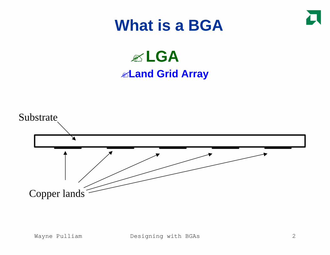
What is a BGA
?LGA?Land Grid Array
Substrate
Copper lands
Wayne Pulliam Designing with BGAs 3
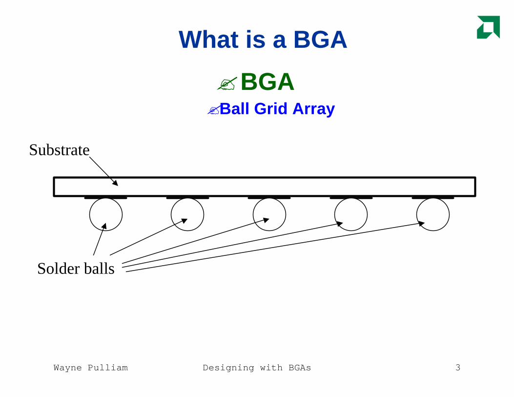
What is a BGA
?BGA?Ball Grid Array
Substrate
Solder balls
Wayne Pulliam Designing with BGAs 4
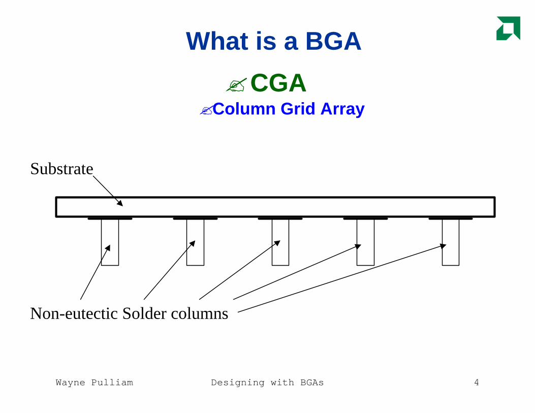
What is a BGA
?CGA?Column Grid Array
Substrate
Non-eutectic Solder columns
Wayne Pulliam Designing with BGAs 5
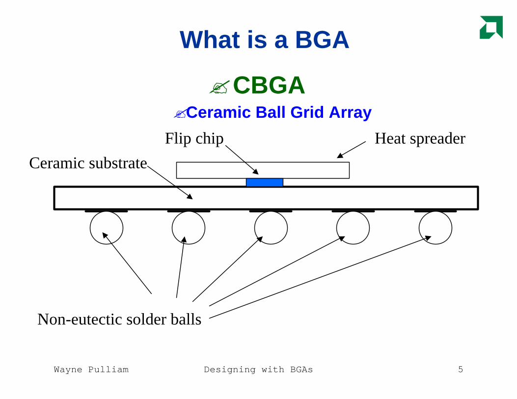
What is a BGA
?CBGA?Ceramic Ball Grid Array
Ceramic substrateHeat spreaderFlip chip
Non-eutectic solder balls
Wayne Pulliam Designing with BGAs 6
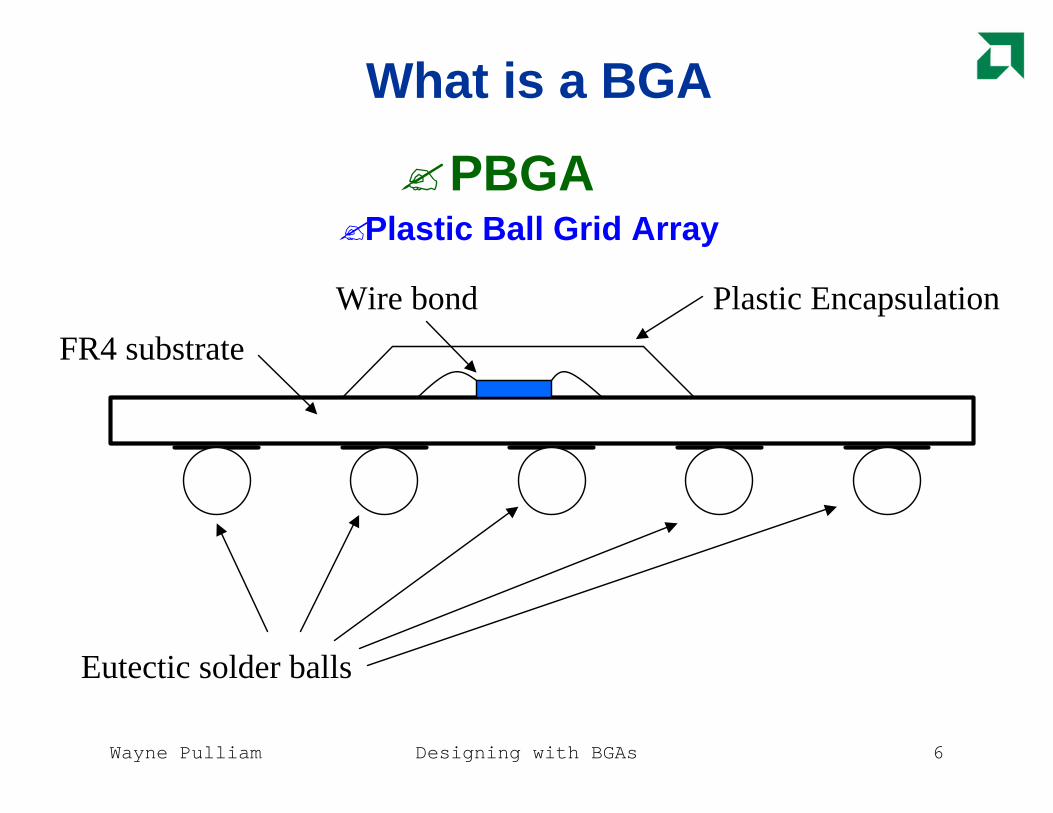
What is a BGA
?PBGA?Plastic Ball Grid Array
FR4 substrateWire bond Plastic Encapsulation
Eutectic solder balls
Wayne Pulliam Designing with BGAs 7
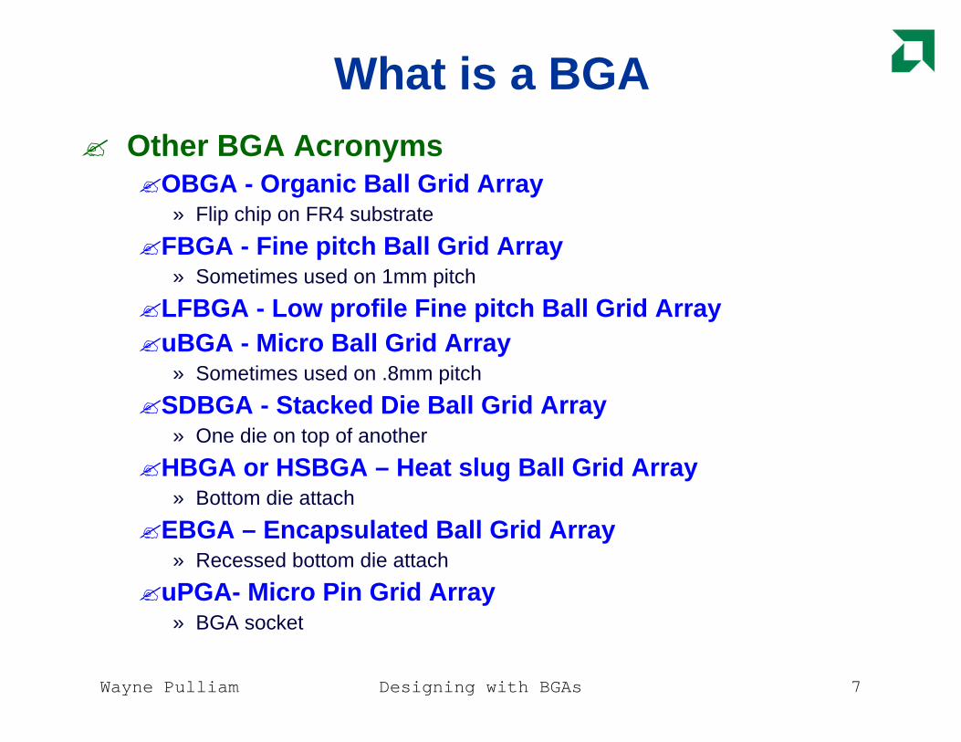
What is a BGA? Other BGA Acronyms
?OBGA - Organic Ball Grid Array» Flip chip on FR4 substrate
?FBGA - Fine pitch Ball Grid Array» Sometimes used on 1mm pitch
?LFBGA - Low profile Fine pitch Ball Grid Array?uBGA - Micro Ball Grid Array
» Sometimes used on .8mm pitch
?SDBGA - Stacked Die Ball Grid Array» One die on top of another
?HBGA or HSBGA – Heat slug Ball Grid Array» Bottom die attach
?EBGA – Encapsulated Ball Grid Array» Recessed bottom die attach
?uPGA- Micro Pin Grid Array» BGA socket

Wayne Pulliam Designing with BGAs 8
What is a BGA
?HBGA?Heat Slug Ball Grid Array
Eutectic solder balls
Heat spreaderSubstrate is usually FR4 Flip chip
Wayne Pulliam Designing with BGAs 9
Plastic Encapsulation
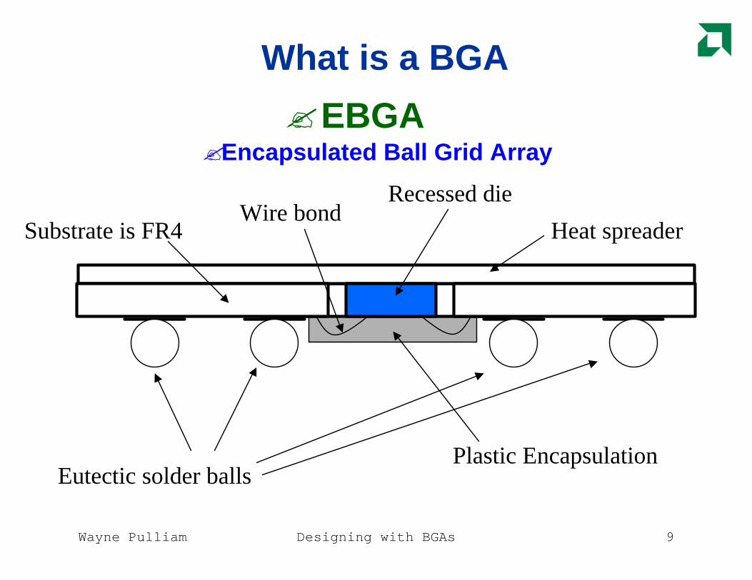
What is a BGA
?EBGA?Encapsulated Ball Grid Array
Eutectic solder balls
Substrate is FR4 Heat spreader
Recessed dieWire bond
Wayne Pulliam Designing with BGAs 10
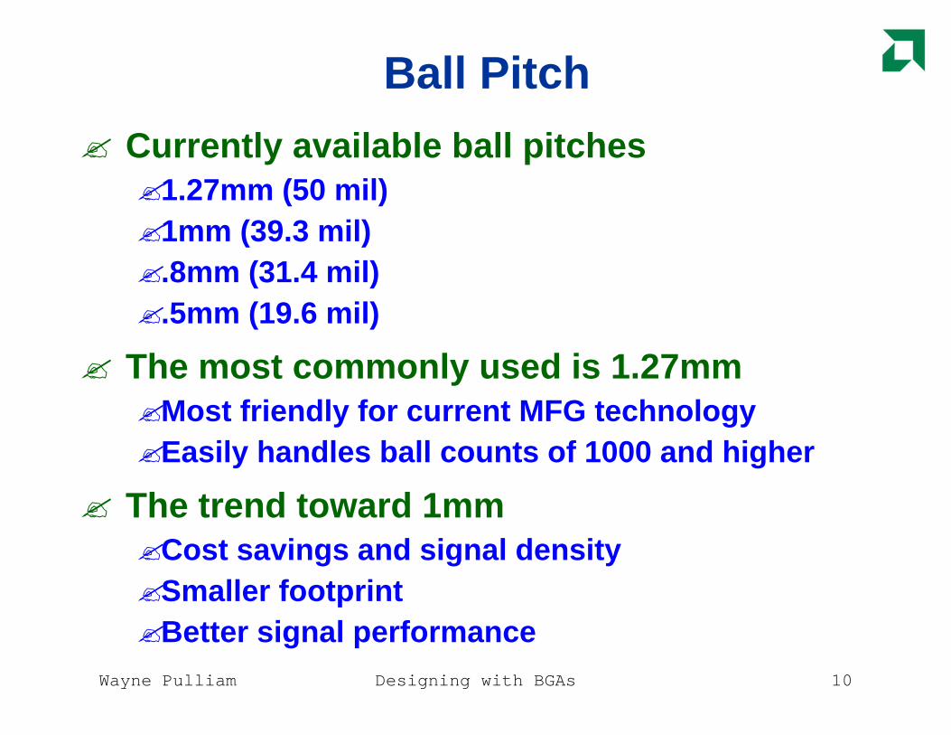
Ball Pitch
? Currently available ball pitches?1.27mm (50 mil)?1mm (39.3 mil)?.8mm (31.4 mil)?.5mm (19.6 mil)
? The most commonly used is 1.27mm?Most friendly for current MFG technology?Easily handles ball counts of 1000 and higher
? The trend toward 1mm?Cost savings and signal density ?Smaller footprint ?Better signal performance
Wayne Pulliam Designing with BGAs 11
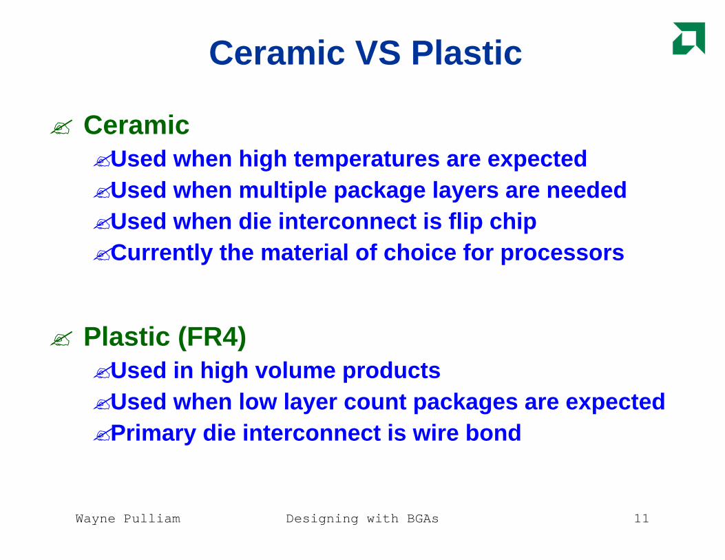
Ceramic VS Plastic
? Ceramic ?Used when high temperatures are expected?Used when multiple package layers are needed?Used when die interconnect is flip chip?Currently the material of choice for processors
? Plastic (FR4)?Used in high volume products?Used when low layer count packages are expected?Primary die interconnect is wire bond
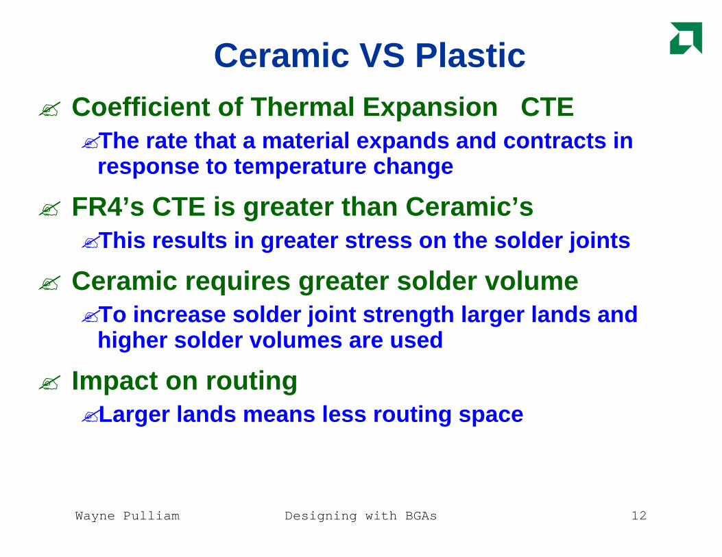
Wayne Pulliam Designing with BGAs 12
Ceramic VS Plastic? Coefficient of Thermal Expansion CTE?The rate that a material expands and contracts in
response to temperature change
? FR4’s CTE is greater than Ceramic’s?This results in greater stress on the solder joints
? Ceramic requires greater solder volume?To increase solder joint strength larger lands and
higher solder volumes are used
? Impact on routing?Larger lands means less routing space
Wayne Pulliam Designing with BGAs 13
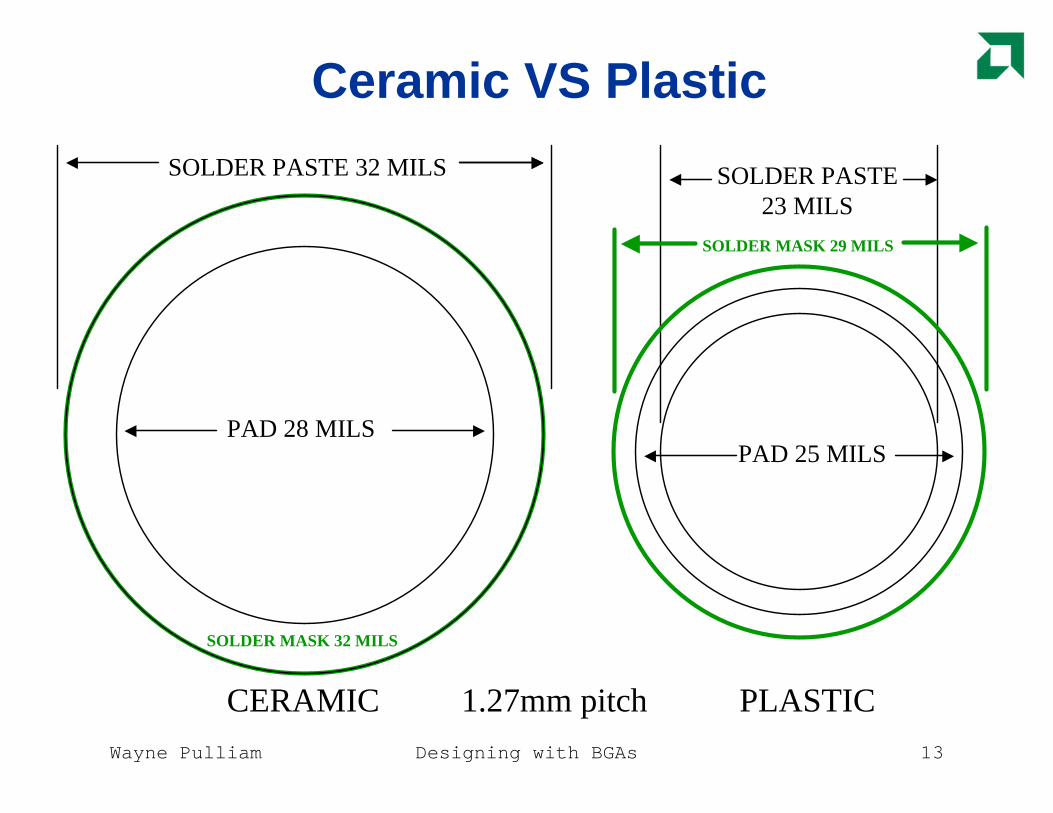
Ceramic VS Plastic
PAD 28 MILSPAD 25 MILS
SOLDER PASTE 23 MILS
CERAMIC PLASTIC1.27mm pitch
SOLDER MASK 32 MILS
SOLDER PASTE 32 MILS
SOLDER MASK 29 MILS

Wayne Pulliam Designing with BGAs 14
Ceramic VS Plastic
PAD 22 MILS
SOLDER PASTE 24 MILS
PAD 20 MILS
SOLDER PASTE 18 MILS
CERAMIC PLASTIC1mm pitch
SOLDER MASK 24 MILS
SOLDER MASK 24 MILS

Wayne Pulliam Designing with BGAs 15
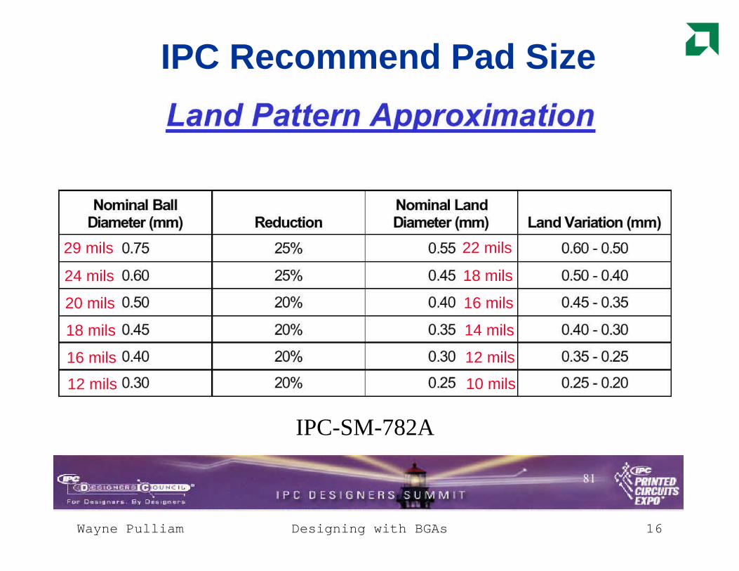
IPC Recommend Pad Size
IPC-SM-782A
Wayne Pulliam Designing with BGAs 16
IPC Recommend Pad Size
29 mils
24 mils
20 mils
18 mils
16 mils
12 mils
22 mils
18 mils
16 mils
14 mils
12 mils
10 mils
IPC-SM-782A

Wayne Pulliam Designing with BGAs 17
BGA Math?Elements of BGA math?Package information
»Substrate material»Ball pitch»Ball size»Number of rows and columns in package»Number of rows with signal balls
?Design parameters»Via size»Trace width»Minimum copper-to-copper spacing
Wayne Pulliam Designing with BGAs 18
BGA Math
? Calculate BGA routing layer requirements?Select ball size?Subtract ball size from ball pitch?Calculate number of traces between pads?Add 1 for outside row of pads?Subtract via size from ball pitch ?Calculate number of traces between vias?Add 1 for outside row of pads?Add via and pads escapes together?This is the number of rows that can be routed in
2 layers?Number of traces between vias for additional
rows per layer
Wayne Pulliam Designing with BGAs 19
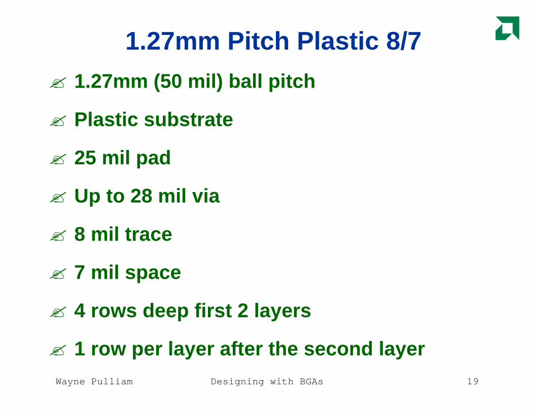
1.27mm Pitch Plastic 8/7? 1.27mm (50 mil) ball pitch
? Plastic substrate
? 25 mil pad
? Up to 28 mil via
? 8 mil trace
? 7 mil space
? 4 rows deep first 2 layers
? 1 row per layer after the second layer
Wayne Pulliam Designing with BGAs 20
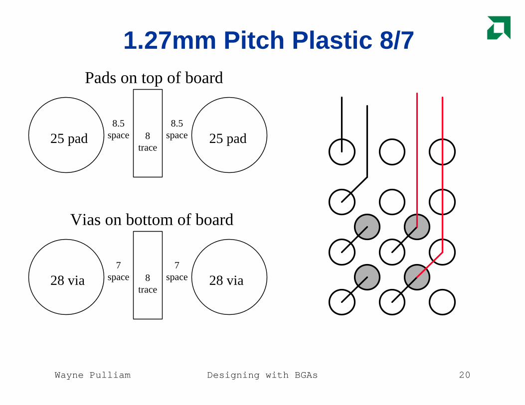
1.27mm Pitch Plastic 8/7
8 trace
8.5 space
8.5 space25 pad 25 pad
Pads on top of board
8 trace
7 space
7 space28 via 28 via
Vias on bottom of board
Wayne Pulliam Designing with BGAs 21
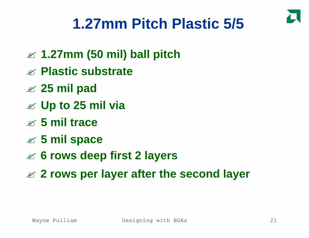
1.27mm Pitch Plastic 5/5
? 1.27mm (50 mil) ball pitch? Plastic substrate? 25 mil pad? Up to 25 mil via ? 5 mil trace ? 5 mil space? 6 rows deep first 2 layers
? 2 rows per layer after the second layer
Wayne Pulliam Designing with BGAs 22
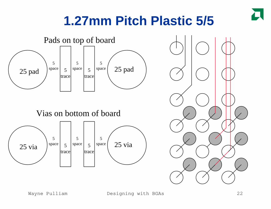
1.27mm Pitch Plastic 5/5
25 pad 25 pad
Pads on top of board
5 trace
5 space5
trace
5 space
5 space
Vias on bottom of board
25 via 25 via5 trace
5 space5
trace
5 space
5 space
Wayne Pulliam Designing with BGAs 23
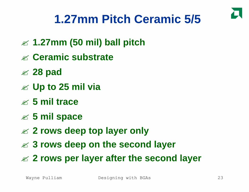
1.27mm Pitch Ceramic 5/5
? 1.27mm (50 mil) ball pitch
? Ceramic substrate
? 28 pad
? Up to 25 mil via
? 5 mil trace
? 5 mil space
? 2 rows deep top layer only? 3 rows deep on the second layer? 2 rows per layer after the second layer
Wayne Pulliam Designing with BGAs 24
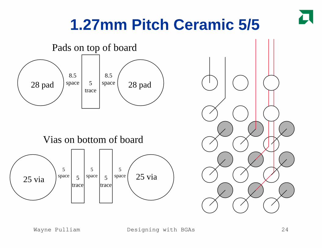
1.27mm Pitch Ceramic 5/5
Vias on bottom of board
25 via 5 trace
5 space 25 via5
trace
5 space
5 space
28 pad 5 trace
8.5 space
8.5 space 28 pad
Pads on top of board
Wayne Pulliam Designing with BGAs 25
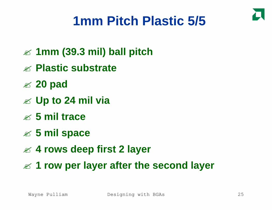
1mm Pitch Plastic 5/5
? 1mm (39.3 mil) ball pitch
? Plastic substrate
? 20 pad
? Up to 24 mil via
? 5 mil trace
? 5 mil space
? 4 rows deep first 2 layer
? 1 row per layer after the second layer

Wayne Pulliam Designing with BGAs 26
1mm Pitch Plastic 5/5
20 pad 5 trace
7 space
7 space 20 pad
Pads on top of board
24 via 5 trace
5 space
5 space 24 via
Vias on bottom of board
Wayne Pulliam Designing with BGAs 27
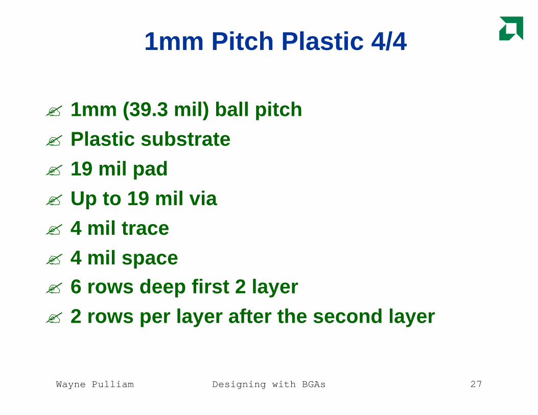
1mm Pitch Plastic 4/4
? 1mm (39.3 mil) ball pitch? Plastic substrate? 19 mil pad? Up to 19 mil via ? 4 mil trace ? 4 mil space? 6 rows deep first 2 layer? 2 rows per layer after the second layer
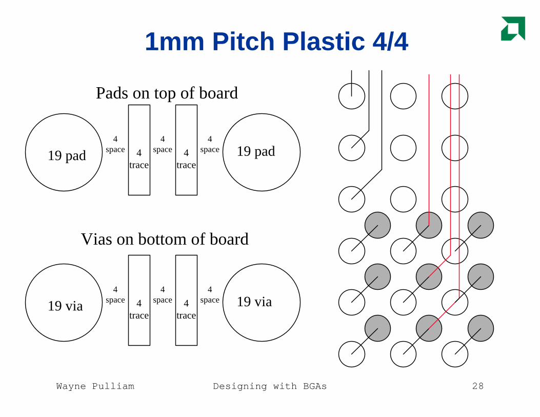
Wayne Pulliam Designing with BGAs 28
1mm Pitch Plastic 4/4
19 pad 4 trace
4 space 19 pad
Pads on top of board
4 trace
4 space
4 space
Vias on bottom of board
19 via 4 trace
4 space 19 via4
trace
4 space
4 space

Wayne Pulliam Designing with BGAs 29
.8mm Pitch Plastic 5/5
? 1mm (31.5 mil) ball pitch
? Plastic substrate
? 16 pad
? Up to 16 mil via
? 5 mil trace
? 5 mil space
? 2 rows deep first 2 layer
? 1 row per layer after the second layer
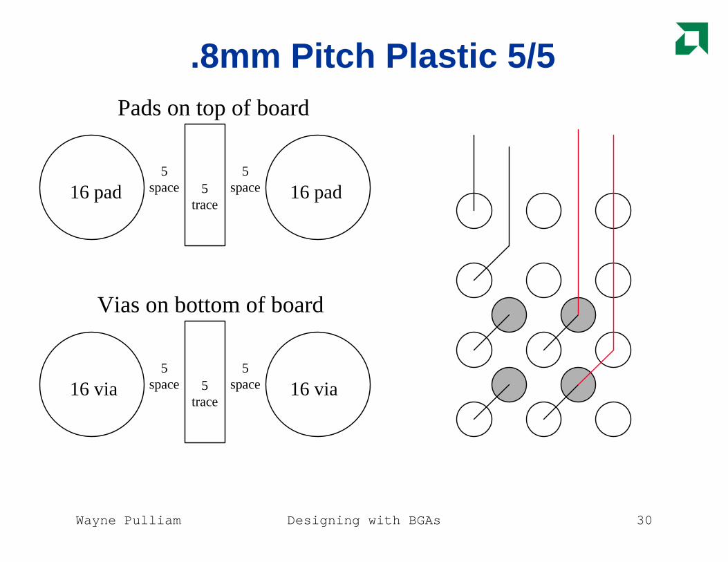
Wayne Pulliam Designing with BGAs 30
.8mm Pitch Plastic 5/5
16 pad 5 trace
5 space
5 space 16 pad
Pads on top of board
16 via 5 trace
5 space
5 space 16 via
Vias on bottom of board
Wayne Pulliam Designing with BGAs 31
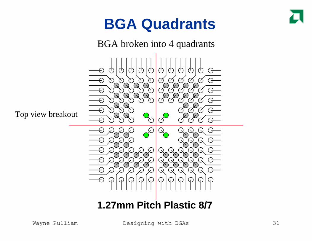
BGA QuadrantsBGA broken into 4 quadrants
Top view breakout
1.27mm Pitch Plastic 8/7

Wayne Pulliam Designing with BGAs 32
BGA QuadrantsBGAs broken into 4 quadrants
Bottom view breakout
1.27mm Pitch Plastic 8/7
Wayne Pulliam Designing with BGAs 33
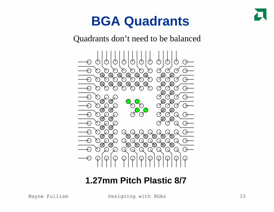
BGA Quadrants
1.27mm Pitch Plastic 8/7
Quadrants don’t need to be balanced
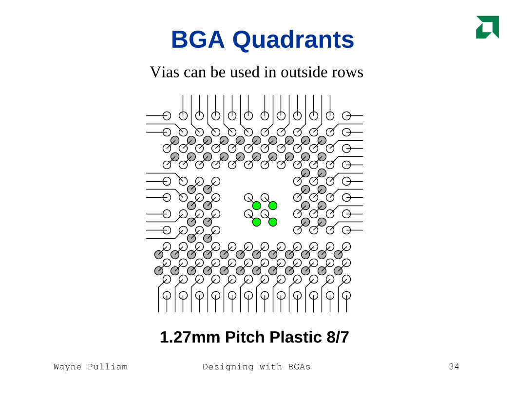
Wayne Pulliam Designing with BGAs 34
BGA Quadrants
1.27mm Pitch Plastic 8/7
Vias can be used in outside rows

Wayne Pulliam Designing with BGAs 35
BGA Quadrants
? Additional routing channels
? Traces can be routed through BGA
? Can reduce length of critical traces
? Provide a path for a last minute trace
? Natural division between signal groups
? Improved power distribution
Wayne Pulliam Designing with BGAs 36
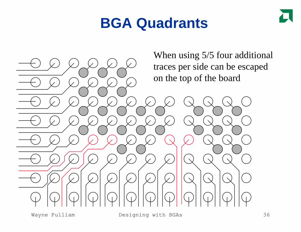
BGA Quadrants
When using 5/5 four additional traces per side can be escaped on the top of the board

Wayne Pulliam Designing with BGAs 37
BGA Quadrants
75 mils can
route seven traces here
When using 5/5 eleven additional traces per side can be escaped on the bottom of the board
2 channels are gained from traces routed on the top of the board
2 in the corner
Wayne Pulliam Designing with BGAs 38
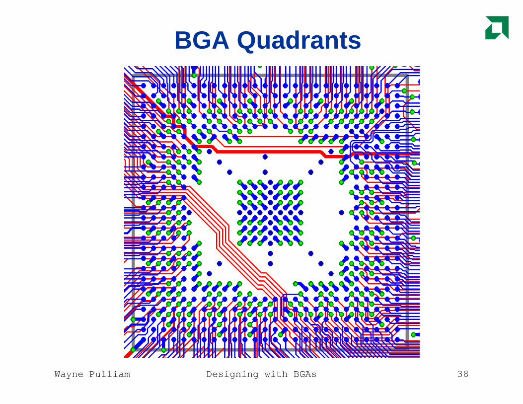
BGA Quadrants

Wayne Pulliam Designing with BGAs 39
Power Delivery
BGA power and ground distribution
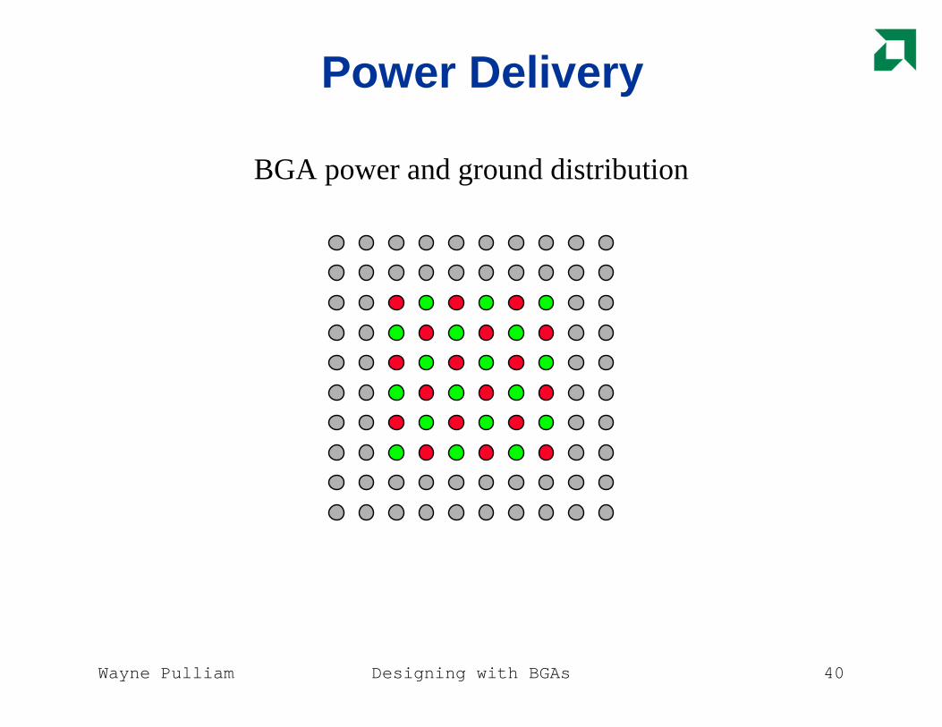
Wayne Pulliam Designing with BGAs 40
Power Delivery
BGA power and ground distribution
Wayne Pulliam Designing with BGAs 41
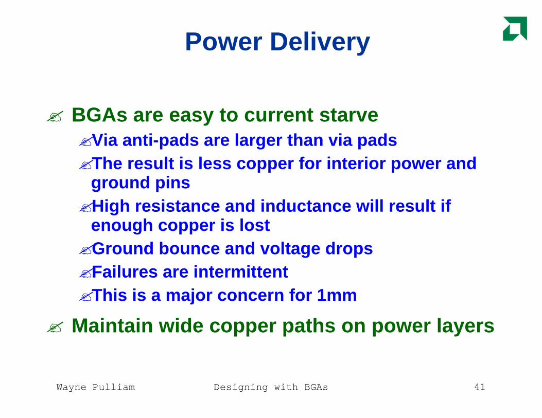
Power Delivery
? BGAs are easy to current starve?Via anti-pads are larger than via pads?The result is less copper for interior power and
ground pins?High resistance and inductance will result if
enough copper is lost?Ground bounce and voltage drops?Failures are intermittent?This is a major concern for 1mm
? Maintain wide copper paths on power layers
Wayne Pulliam Designing with BGAs 42
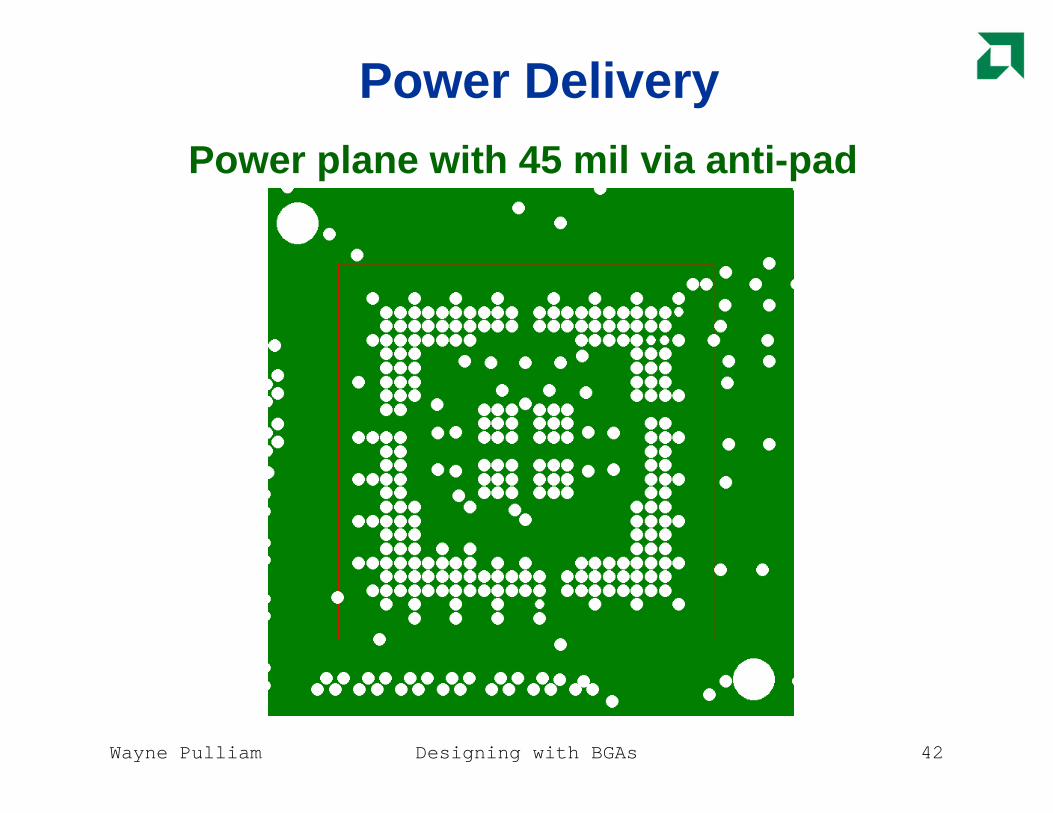
Power DeliveryPower plane with 45 mil via anti-pad

Wayne Pulliam Designing with BGAs 43
50
25 pads
25 vias
15 drill
70
10
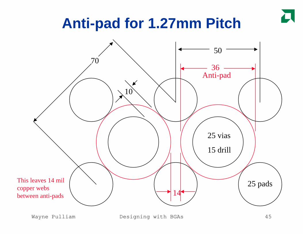
Anti-pad for 1.27mm Pitch
5
45Anti-pad
This leaves 5 mil copper webs between anti-pads
Wayne Pulliam Designing with BGAs 44
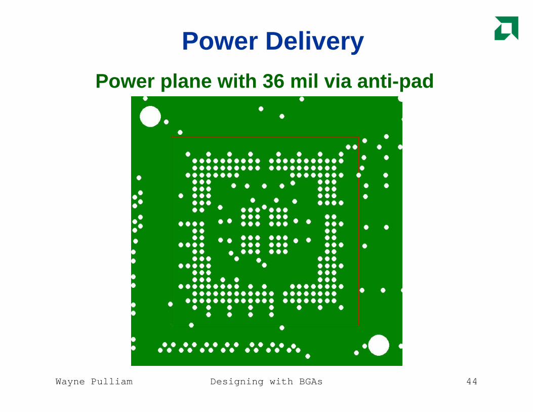
Power DeliveryPower plane with 36 mil via anti-pad
Wayne Pulliam Designing with BGAs 45
Anti-pad for 1.27mm Pitch
14
36Anti-pad
This leaves 14 mil copper webs between anti-pads
50
25 pads
70
10
25 vias
15 drill

Wayne Pulliam Designing with BGAs 46
Anti-pad for 1.27mm Pitch
18
32Anti-pad
This leaves 18 mil copper webs between anti-pads
50
25 pads
70
10
25 vias
15 drill
Wayne Pulliam Designing with BGAs 47
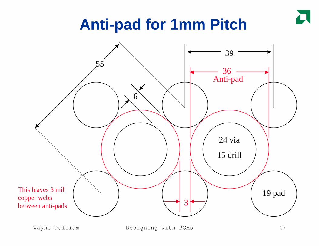
Anti-pad for 1mm Pitch
39
19 pad
24 via
15 drill
55
6
3
36Anti-pad
This leaves 3 mil copper webs between anti-pads
Wayne Pulliam Designing with BGAs 48
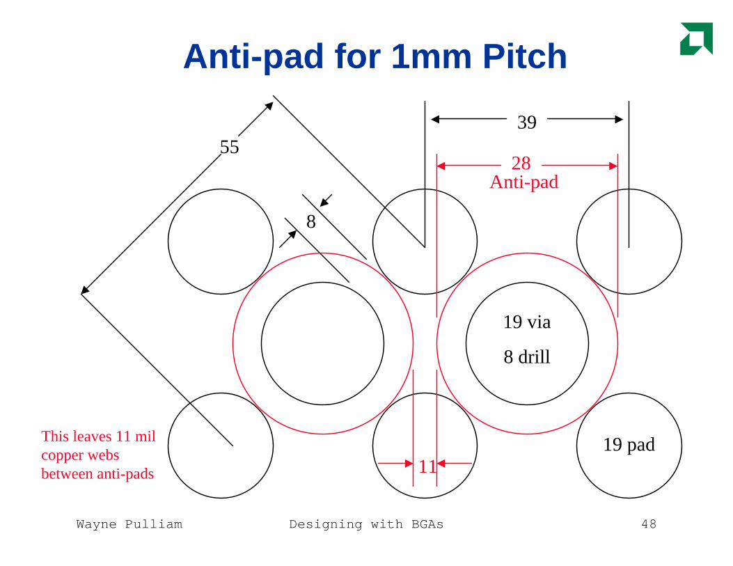
Anti-pad for 1mm Pitch
39
19 pad
19 via
8 drill
55
8
11
28Anti-pad
This leaves 11 mil copper webs between anti-pads
Wayne Pulliam Designing with BGAs 49
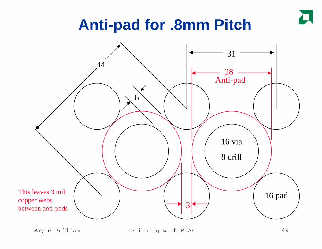
Anti-pad for .8mm Pitch
31
16 pad
16 via
8 drill
44
6
3
28Anti-pad
This leaves 3 mil copper webs between anti-pads
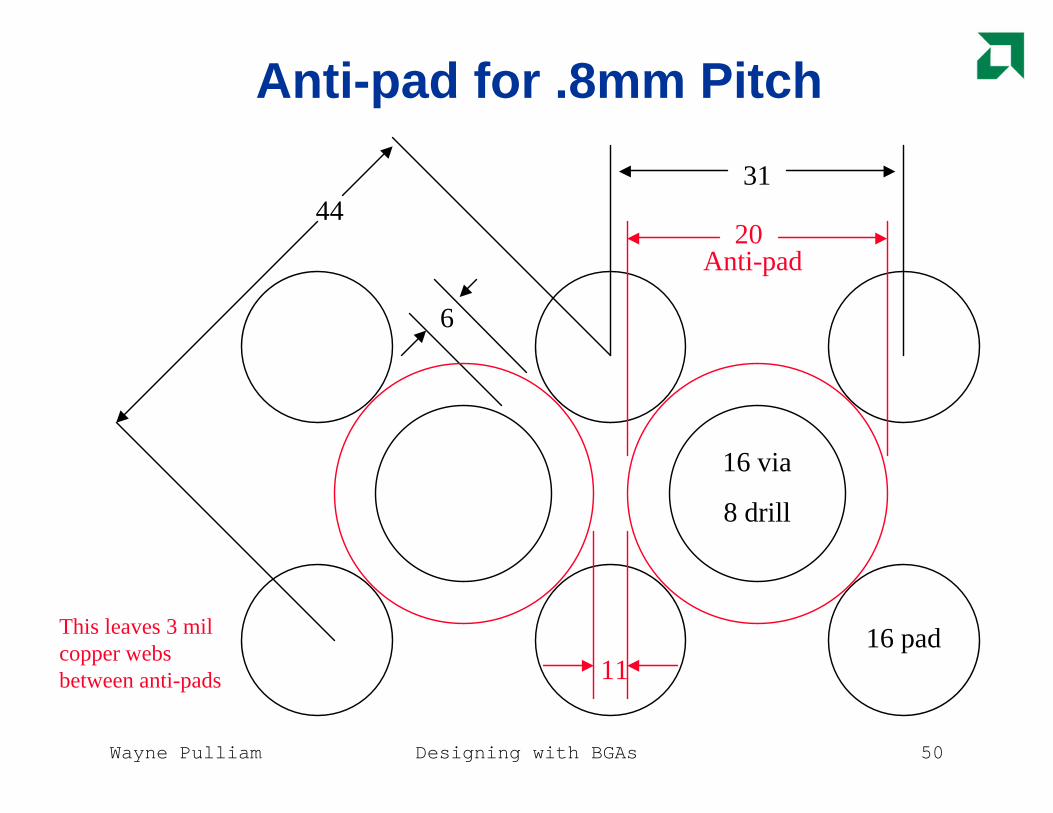
Wayne Pulliam Designing with BGAs 50
Anti-pad for .8mm Pitch
31
16 pad
16 via
8 drill
44
6
11
20Anti-pad
This leaves 3 mil copper webs between anti-pads
Wayne Pulliam Designing with BGAs 51
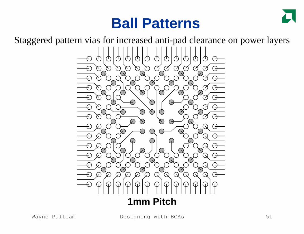
Ball PatternsStaggered pattern vias for increased anti-pad clearance on power layers
1mm Pitch
Wayne Pulliam Designing with BGAs 52
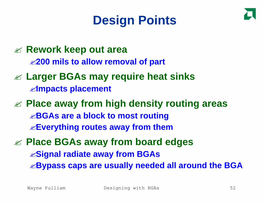
Design Points
? Rework keep out area?200 mils to allow removal of part
? Larger BGAs may require heat sinks?Impacts placement
? Place away from high density routing areas?BGAs are a block to most routing?Everything routes away from them
? Place BGAs away from board edges?Signal radiate away from BGAs ?Bypass caps are usually needed all around the BGA

Wayne Pulliam Designing with BGAs 53
Design Points
? Mask over vias under BGA?A precaution taken to avoid problem that can occur
during wave solder
? 75% rule for power traces?Keep traces below 75% of the pad width to prevent
solder wicking
? Copper fills or pours should not be used?Pouring copper around BGA pads changes the pad
geometry which leads to reduces solder joint reliability
Wayne Pulliam Designing with BGAs 54
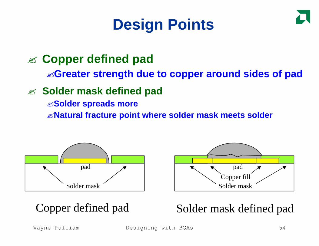
Design Points
? Copper defined pad?Greater strength due to copper around sides of pad
Copper defined pad Solder mask defined pad
pad
Solder mask
pad
Solder maskCopper fill
? Solder mask defined pad?Solder spreads more?Natural fracture point where solder mask meets solder
Wayne Pulliam Designing with BGAs 55
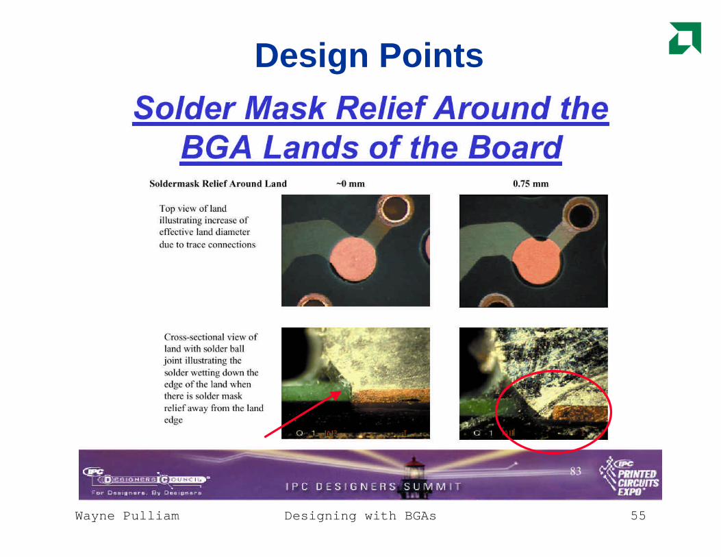
Design Points
Wayne Pulliam Designing with BGAs 56
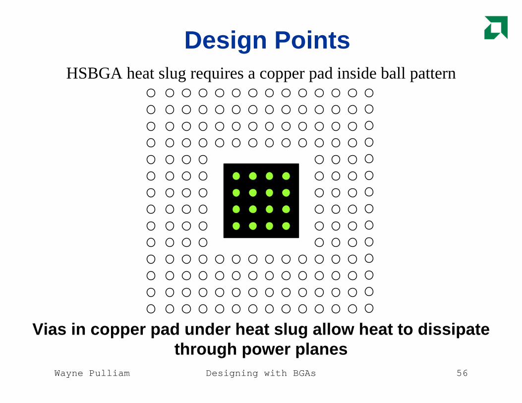
Design Points
Vias in copper pad under heat slug allow heat to dissipate through power planes
HSBGA heat slug requires a copper pad inside ball pattern
Wayne Pulliam Designing with BGAs 57
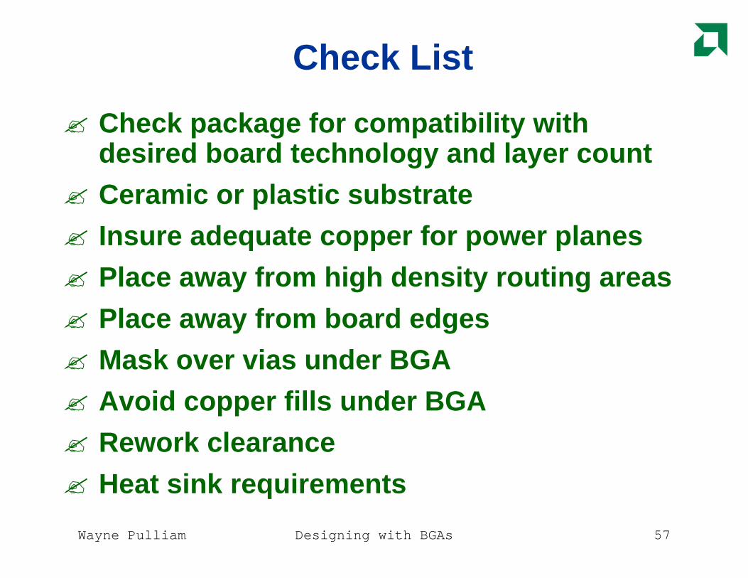
Check List
? Check package for compatibility with desired board technology and layer count
? Ceramic or plastic substrate? Insure adequate copper for power planes? Place away from high density routing areas? Place away from board edges? Mask over vias under BGA? Avoid copper fills under BGA? Rework clearance? Heat sink requirements

Wayne Pulliam Designing with BGAs 58
Web Sites to check out? National Instruments application note
» http://www.national.com/packaging/appnote_bga.html
? Intel application note» http://www.intel.com/design/packtech/ch_14.pdf
? Motorola application note » http://www.cloudcaptech.com/MPC555%20Resources/Board%20guidelines/AN1231.pdf
? Flotherm BGA thermal modeling» http://www.flotherm.com/technical_papers/t169/t169.jsp
? Semiconductor International article» http://www.semipark.co.kr/upload1/Ball%20Grid%20Arrays.pdf
? Semitech BGA failure testing» http://www.sematech.org/public/docubase/document/3957axfr.pdf
? Ball Grid Array Technology?Book table of contents (last printing 95)
» http://www.smtplus.com/bgat.htm
? Email: [email protected]
Layout Design Concerns When Designing With Ball Grid Array Packages
This paper will help speed you on your way to designing with BGAs. It is a combination of information I have learned and techniques that I have developed to make designing with the BGA easy. Why BGAs are here to stay As IO counts on integrated circuits continue to rise there will be more grid array packages coming into use. These packages are manufacturing friendly. They have large numbers of connections in a small area while maintaining wide contact spacing. During reflow, the part will actually float and center itself due to the surface tension of the liquid solder. All of the leads on a BGA are under the plane structure of the package. The leads are also considerably shorter than other high-density packages. These factors help reduce EMI emissions while improving signal integrity. They also have excellent power distribution capabilities. Because of the high pin count, a larger percentage of pins can be dedicated to power and ground connects. Some BGAs boast signal-to-power pin ratios as high as 50%. This greatly reduces inductance and if properly distributed improves AC return path. Capacitance can be built into the internal substrate structure or added directly to the package to increase power performance. Terminology The following are basic terms used with grid arrays.
• Substrate: Describes the interconnect package material.
• Ceramic: Material commonly used in grid array substrates.
• Organic: A term used for FR4 when it is used as a substrate material.
• Eutectic: Describes the 37:63 tin-to-lead composition of solder.
• Non-eutectic: Describes a tin-to-lead composition other that 37:63. Non-eutectic solder-balls or columns are typically a 90:10 tin-to-lead composition.
Types of grid arrays A land grid array (LGA) is a package with no balls or solder columns attached. These are often used with sockets. It is also a common practice to test the LGA package before adding balls or columns. A ball grid array (BGA) is a land grid array with solder-balls attached. A column grid array (CGA) is a land grid array with solder columns attached. A ceramic ball grid array (CBGA) is a land grid array made with a ceramic substrate with solder-balls attached. An organic ball grid array (OBGA) is a land grid array made with an organic substrate with solder-balls attached. A ceramic column grid array (CCGA) is a land grid array made with a ceramic substrate with solder columns attached. An organic column grid array (OCGA) is a land grid array made with an organic substrate with solder columns attached. All of these different acronyms fall under the generic term BGA. Solder ball types Solder-balls come in two types: eutectic and non-eutectic. Eutectic solder-balls melt at the same temperature as the solder paste used in the reflow process. The solder ball mixes with the solder paste on the board and the substrate floats on bubbles of solder until the solder hardens. The hardened solder is oval in shape as the weight of the substrate collapses the solder-balls. Solder paste volume will vary from one assembly shop to another. Some assembly shops actually reflow BGAs with no solder paste on the board. They simply allow the solder-balls to collapse on the lands. Non-eutectic solder-
balls don’t collapse during reflow. They retain their shape and keep the substrate higher from the PCB. This, in conjunction with a higher solder volume, increases solder joint strength. Non-eutectic solder columns are also use for interconnect. The use of columns increases the gap between the PCB and the package. This increases solder joint flexibility, which increases the reliability of the connection. Substrates Grid array substrate material determines what type of solder ball will be required. There are two primary types of material in use today. FR4 – or organic – is by far the most common. It is also the most friendly for routing. Organic substrates use eutectic solder-balls. The other material is ceramic. It is used when many package layers are needed, extremely high temperatures are expected, or flatness is an issue (as is the case with most flip chip application). Ceramic material expands at different rate than FR4. Because of this, greater solder joint strength is needed. Ceramic substrates use non-eutectic solder-balls or columns. Increasing the size of the land on the PCB and increasing the volume of solder is also required to reach the desired solder joint strength. The impact on the routing is the loss of area due to the increased pad size. Pad size A typical 1.27mm pitch ceramic part requires a 28mil pad with 32mil solder paste (These sizes are interchangeable for non-eutectic solder-balls or columns). A typical 1.27mm organic part will use a 25mil pad with 23mil solder paste. Be sure that you know what material the BGA substrate is made of before you begin. Typical 1mm package pads are 20mils with 18mil solder paste. The only 1mm packages I have used have organic substrates. If you use a 1mm ceramic package increase the pad and paste diameters as much as possible. I use 4mils over the diameter solder mask openings on all features. As always, check with your
assembly shop to confirm pad size and paste volume. These numbers are process-specific and may not be used by all assemblers. Calculate the number of layers required for a specific package Using this formula, you can quickly estimate the number of layers needed for a given BGA. First, collect the information needed to calculate layer usage. The information from the package is the substrate material, the ball pitch, the ball pattern and a map of the signal locations in the ball pattern. The rest of the information will be in the PCB design parameters. These are via pad size, trace width and copper-to-copper spacing. The substrate material and the ball pitch will determine the pad size. If you subtract the pad size from the ball pitch you will get the space between the pads. This number can be divided by the trace and space to determine how many wires can be routed between pads. Add 1 to the number of wire that can be routed between pads and you have the number of ball rows that can be escaped from the package on the component routing layer. You can use the same formula for the first via though layer simply substitute via size for pad size. After the first additional layer, use the number of wires that will fit between the vias per layer. We add the additional row because the outside row of pads and the first row of vias are free. No features block their routing path. Example: The substrate material is FR4 and the ball pitch is 1.27mm (50mils). This makes the pad size 25mils. The routing rules are 5mil traces and 5mil spaces, with a 25mil via pad. Subtract the pad size (25) from the pitch (50) to yield the space between pads (25). Divide the space (25) by the trace and space (5) for a total of 3 spaces and 2 traces. Add (1) to the number of traces (2) for the total (3). This is the number of rows that can be escaped on the top layer. With via size, the same as the pad, the math will be the same. So add 3 more rows of balls for the

first via through layer. So we get 6 rows of balls escaped in 2 layers as long as the outside rows are escaped on the top layer, and we will get 2 rows of balls escaped for each additional layer added to the board. BGA escape patterns Establishing a regular escape pattern when routing a BGA has many benefits. Breaking the BGA into quadrants allows for the routing of traces through the BGA. These routing channels can save you in a pinch. They can also be used to create a natural division between signal groups. If you are trying to reduce layer count, then the quadrants also allow for additional rows of balls to be escaped. If outside row signals need to change layer, then do so at some distance away from the BGA. If vias are used in the outside rows of balls, it is guaranteed that additional layers will be required. I have only seen two 1.27mm BGA parts that required more than 2 signal layers to route. Both of them had 30 or more rows/columns, over 900 balls and the signal balls were 8 rows deep. Power delivery Using a quadrant breakout also helps current flow on the plane layers. Breaking the BGA out in quadrants creates wide straps of copper on the planes. This helps power distribution because most BGAs have the majority of their power and ground pins on the interior rows. If the power planes lose too much copper to via clearances, then a high inductance path is created. The catchall standard negative layer via clearance is 30mils over the drill. This is likely to cause you problems. With a 15mil drill, the clearance is 45mils. Subtracted from the pitch of 50mils, this leaves you 5mils of copper between vias on the power planes. If this clearance is used on a BGA requiring high current, then even the heavy copper straps created by the quadrants won’t save you. The high inductance path may cause the part to not work at all. More commonly, the resulting ground bounce will produce
intermittent problems. This is a very difficult problem to troubleshoot. I strongly recommend that via clearance on power layer not exceed 35mils. This gives you 15mil wide connections between all of your vias. This is in addition to the quadrant straps. Issues with 1mm BGAs There is a general trend in packaging to move to 1mm BGAs. The 1mm package represents a large cost saving for the component manufacturer. It also reduces trace length, reduces inductance for power delivery and shorten return path for AC current. All of these are good reason to use 1mm packages. At the board level the 1mm package is pushing the envelope. To escape 6 rows deep on a PCB in 2 layers requires a 19mil pad, 19mil via with an 8mil drill and the use of 4mil traces with 4mil space. The reduction of feature sizes represents added cost at most fabrication houses. From a design stand point you are faced with the choice of design the entire board with 4mil traces or dealing with the changing trace and space for all signals connection to the BGA. Choosing to avoid the trace width issue by adding layers is not an end all problem solver. You get to use 5mil trace and space and you can squeeze a 24mil via with a 12mil drill. This looks good until you examine the power planes. With a 35mil anti-pad the copper webbing between the vias is only 4mils. Copper features that small on 1-ounce planes are likely to be etched away. Even when an 8mil drill is used the anti-pad is still 28mils. (20mils over the drill) Leaving 11mil wide webs through the via pattern on power layers. If you are designing a cost sensitive product examine any 1mm BGAs carefully before using them in your design. If you are planning to use high ball count BGAs with pitches smaller than 1mm you should be prepared to use some form of HDI
(high density interconnect) micro-via technology. General Design Guidelines Placement It is best to keep BGAs away from other high-density parts and board edges. If your board has low layer count, then the BGA is a block to routing as all available routing layers are used to escape. Connections radiate away from BGAs placing them too close to a board edge will make them impossible to escape without adding additional layers. On single sided assemblies decoupling caps also become an issue when to close to the board edge. Check the manufacturer’s specifications for heat sink requirements. Many BGAs are high current and require heat sinks. Some attach with adhesive directly to the package while others require mounting holes. Remember to account for them during placement. Rework and heat sinks A consideration for the footprint is a rework head keep out. A 200mil radius keep-out will generally be good. Check with your assembler the keep-out area will vary between shops. Many design engineers will sacrifice this area for the sake of decoupling capacitors and other critical components. Because of the friendly nature of the BGA in the manufacturing process, this is usually not a problem. Copper fills, power trace widths & solder mask The use of copper fills under BGAs is not good design practice. The farther from the center of the part the fill is, the greater the risk. When copper is solid around a pad, the geometry of the pad changes from copper-defined to solder-mask-defined. This greatly reduces the solder joint strength. A copper defined pad allows the solder to flow down the sides of the pad. This makes the joint less likely to fracture. This is a long-term reliability issue. Another pad geometry issue
is trace width. This has to do with the conduction of heat. If the trace width is equal to or greater than the pad size, then there is a possibility of solder wicking during reflow or wave solder. Solder will reflow and wick to the source of the heat. This leaves the pad with no solder. To help prevent this, use the 75% rule. The trace should not exceed 75% of the pad width. This restricts heat conduction. The usual fix for this problem, moving the via away from the pad, is not an option on a BGA. Vias under the BGA can cause another problem during wave solder. Solder can come through the vias and cause shorts under the BGA. This has a simple fix. Mask over all vias under the BGA. BGA CHECK LIST
1. Identify substrate material 2. Determine target layer count 3. Check ball pitch for compatibility
with desired board technology 4. Insure adequate copper for power
plane connection 5. Discuss the need for rework
clearance 6. Determine if a heat sink is
required 7. Place away from other high-density
parts 8. Place away from board edges 9. Use quadrants to escape the BGA 10. No copper fills under BGAs 11. Mask over vias under BGAs 12. 75% rule for traces
Summary If all of these issues are accounted for, then the BGA is a very effective package for high-density low layer count boards.
![de partido a su piscina… - BINDER · Tipo BGA 160 BGA 215 BGA 275 BGA 320 BGA 430 BGA 550 BGA 600 BGA 1200 Tensión de conexión [VAC] 230 230 230 230 230 230 230 230 Rango de frecuencia](https://img.pdfslide.net/doc/110x75/5c132e8509d3f26c7c8c5e0d/de-partido-a-su-piscina-binder-tipo-bga-160-bga-215-bga-275-bga-320-bga-430.jpg)