Embed Size (px)
Citation preview
Why Did the Electron Cross the Road? A Scanning TunnelingMicroscopy (STM) Study of Molecular Conductance for the PhysicalChemistry LabBradley W. Ewers, Amanda E. Schuckman,§ and James D. Batteas*
Department of Chemistry, Texas A&M University, College Station, Texas 77842-3012, United States
*S Supporting Information
ABSTRACT: A series of experiments employing scanning tunnelingmicroscopy (STM) have been developed for the physical chemistry laboratory.These experiments are designed to engage students in cutting edge researchtechniques while introducing and reinforcing topics in physical chemistry,quantum mechanics, solid-state chemistry, and the electronic structure ofmolecules and materials. In the first of three experiments, students areintroduced to the basics of STM operation while imaging and conductingspectroscopy on the highly oriented pyrolytic graphite (HOPG) surface.Images of the surface are used to determine the crystal structure of thematerial, and scanning tunneling spectroscopy is used to determine theelectronic properties of the material and study the tunneling phenomenon. In the second experiment, the students image theAu(111) surface as well as a series of alkanethiol self-assembled monolayers (SAMs) of different chains lengths on the Au(111)surface. They examine the structural and electronic properties of the metal surface and the adlattice structure of the film. Finally,in the third experiment, the students examine the conductance of molecules adsorbed onto the Au(111) surface, including thealkanethiol SAMs and a thiol-tethered porphyrin molecule or a dimercaptostilbene embedded into the SAM matrix. Bymeasuring the tunneling efficiency and spectroscopic characteristics of these molecules, the students can explore the relationshipbetween chemical structure and charge transport efficiency. The experiments provide advanced chemistry students anopportunity to view and study materials at the atomic and molecular length scales and provide an opportunity to apply theirunderstanding of quantum mechanical concepts to real systems.
KEYWORDS: Upper-Division Undergraduate, Laboratory Instruction, Physical Chemistry, Hands-On Learning/Manipulatives,Nanotechnology, Physical Properties, Spectroscopy, Surface Science
Scanning probe techniques, including scanning tunnelingmicroscopy (STM), atomic force microscopy (AFM), and
the many derivatives of these techniques, are gainingconsiderable traction in chemical and biological investigationsand the field of materials science and engineering in general.1
Familiarity with these techniques will help undergraduatestudents explore how modern physical chemistry and analyticalmethods are applied in research. We have developed a physicalchemistry laboratory with this in mind, focused on demonstrat-ing cutting edge techniques and instrumentation used bychemists, including in particular STM. Not only does this offerstudents exposure to such relevant techniques, it also reinforcestheir understanding of quantum mechanics and the chemicalstructure of solids. Several experiments have been reported thatintroduce students to the STM in the teaching laboratory, eachwith its own unique focus and goals including the study ofsurface structure,2 adsorbate structure and intermolecularinteractions,3,4 nanomaterials,5 and reaction kinetics.6 Thisexperiment introduces a similar series of topics, though withconsiderable emphasis on the mechanisms and quantummechanical process of tunneling as well as the relationshipbetween molecular structure and electron transport. The topicsconsidered in this series include the basics of electron tunneling
and the quantum mechanical description of this phenomenon;the structure of crystals, surfaces, and adlayers; solid-stateproperties of materials; and investigation of charge transfermechanisms through molecules using scanning tunnelingspectroscopy (STS), the latter being relevant to a range ofsubjects including biological systems, the development ofphotovoltaic and other molecular or organic electronicsapplications and incorporating discussions of the relationshipsbetween chemical and electronic structure of complexmolecules.The experiments described herein are part of a physical
chemistry laboratory in the first semester of a two-semestersequence (1 credit each) focusing on the theme of quantummechanics, which parallels the physical chemistry lecturesequence that covers quantum mechanics in the first semesterand thermodynamics in the second semester. Students arerequired to complete the prerequisite lecture in advance oftaking the lab. The laboratories are taken by a mix of third-year(∼20%) and fourth-year (∼80%) students. This experiment isconducted over a three-week span and is broken into three
Published: January 8, 2014
Laboratory Experiment
pubs.acs.org/jchemeduc
© 2014 American Chemical Society andDivision of Chemical Education, Inc. 283 dx.doi.org/10.1021/ed400418h | J. Chem. Educ. 2014, 91, 283−290
distinct parts. The first week is reminiscent of many priorstudies,3,4,7 introducing the fundamentals of STM. The studentsbegin by characterizing highly oriented pyrolytic graphite(HOPG), as this surface is easily prepared and atomicresolution of the surface is achieved with minimal effort.Here, the students learn about the structure of solids andsurfaces and begin their investigation into the electrontunneling process with spectroscopic measurements whilefamiliarizing themselves with the instrumentation and imagingprocess. In the second week, the students examine the surfaceof gold, with and without alkanethiol self-assembled mono-alyers (SAMs). In addition to reinforcing topics discussed inthe first experiment, this section introduces the concept ofsurface adsorbates and their adlattice structure and presents thenotion of electron tunneling through different mediums.Finally, in the third week, the students examine chargetransport through a thiol-tethered porphyrin molecule, whereinthey are encouraged to consider the structure of the moleculeand measurements made both by imaging and spectroscopy, aswell as consultation with the literature, to determine themechanism of electron transport through the molecule. Eachexperiment is designed to be wholly conducted within 3 h,including sample preparation, instrument setup, and clean up,the vast majority of which is conducted by the students underthe guidance of an instructor. Although the molecule we haveused is unique to our physical chemistry lab, we alsodemonstrate here the use of a 4,4′-dimercaptostilbene that iscommercially available.
■ EQUIPMENT AND MATERIALS
A Nanosurf Easyscan2 STM (Nanosurf; Liestal, Switzerland)with a 500 nm low current scanner was used. Pt/Ir tip wire(Nanoscience Instruments, Phoenix, AZ, 0.25 mm diameter)was used, using mechanical cleaving performed initially by theinstructor for demonstration but ultimately by the studentsthemselves. HOPG (Nanoscience Instruments) was cleavedprior to imaging with scotch tape to present a clean surface.Flame-annealed Au on mica substrates obtained from AgilentTechnologies (Phoenix, AZ) and Phasis (Geneva, Switzerland)were cleaned by UV−ozone exposure immediately prior to use.Molecules used included decanethiol, dodecanethiol, octadeca-nethiol, and 4,4′-dimercaptostilbene and were obtained fromSigma Chemicals and used as received. For studies of molecularconductance, a tailor-made thiol-tethered freebase porphyrinwas used, and its synthesis and conductance properties havebeen previously described.8 This experiment was alsodemonstrated with the dimercaptostilbene molecule. Imageanalysis was performed using the freely available Gwyddionsoftware package.9 Complete details of the instrumentation,methods, and implementation of these instructional experi-ments may be found in the Supporting Information.
■ HAZARDS
Gloves and goggles should be worn during all sample andsolution preparation as well as during handling of the samplesand the scanning tunneling microscope. Decanethiol, dodeca-nethiol, and octadecanethiol are irritants, and these along with4,4′-dimercaptostilbene are highly toxic if consumed. Tetrahy-drofuran (THF) and ethanol are flammable. All solvents andchemicals should be used in a chemical hood to minimizeexposure.
■ EXPERIMENTAL DETAILS
Week 1: The Structure and Electronic Properties of HighlyOriented Pyrolytic Graphite (HOPG)
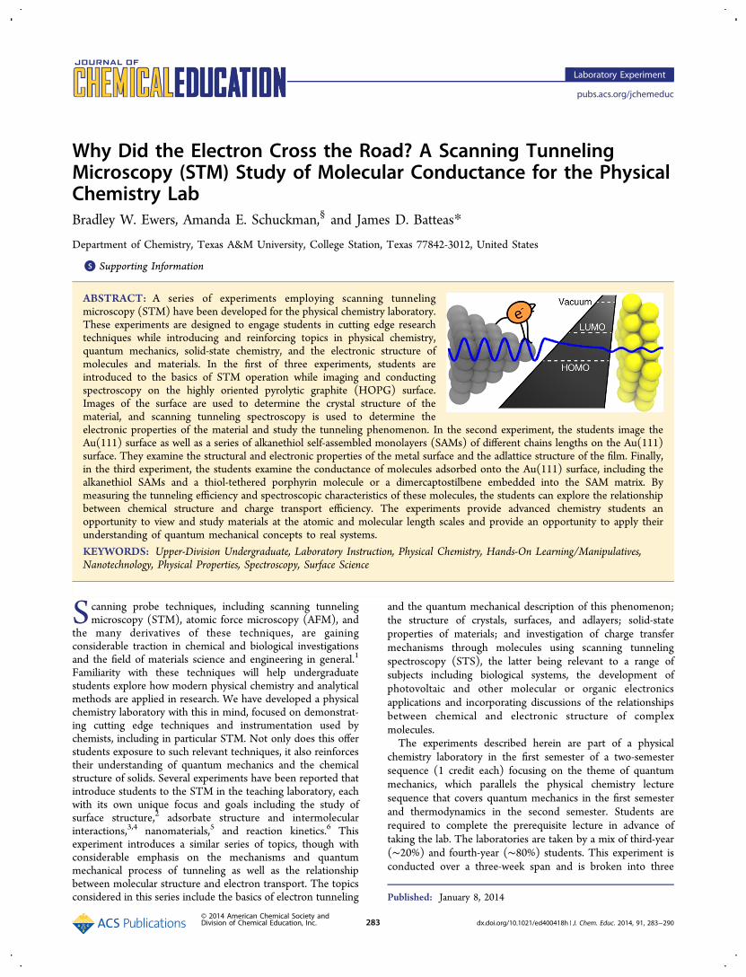
Many previous reports have been made using HOPG toillustrate the capabilities of STM and introduce students to theexamination of atomic structure,3,4,7 and this part of theexperiment is similar. An image of the HOPG surface collectedby a student group is shown in Figure 1 along with a Fourier-
transformed image that clearly shows the lattice structure of thegraphite surface. We find that guiding the students through thisfiltering process introduces students to concepts of data andimage processing and visually illustrates this important noise-reduction technique. The students are instructed to use theimages to reconstruct the crystalline lattice from the measureddimensions of the surface lattice and interlayer spacing,familiarizing themselves with the concepts of a crystal latticeand how STM can be used to deduce the crystal lattice basedon surface measurements. Additionally, the HOPG surfaceconveniently illustrates that STM is not sensitive to nuclearpositions but rather to electronic state density, giving rise to thecontrast observed between the two unique atoms in the surfaceunit cell.The relevant quantum mechanical concepts are also first
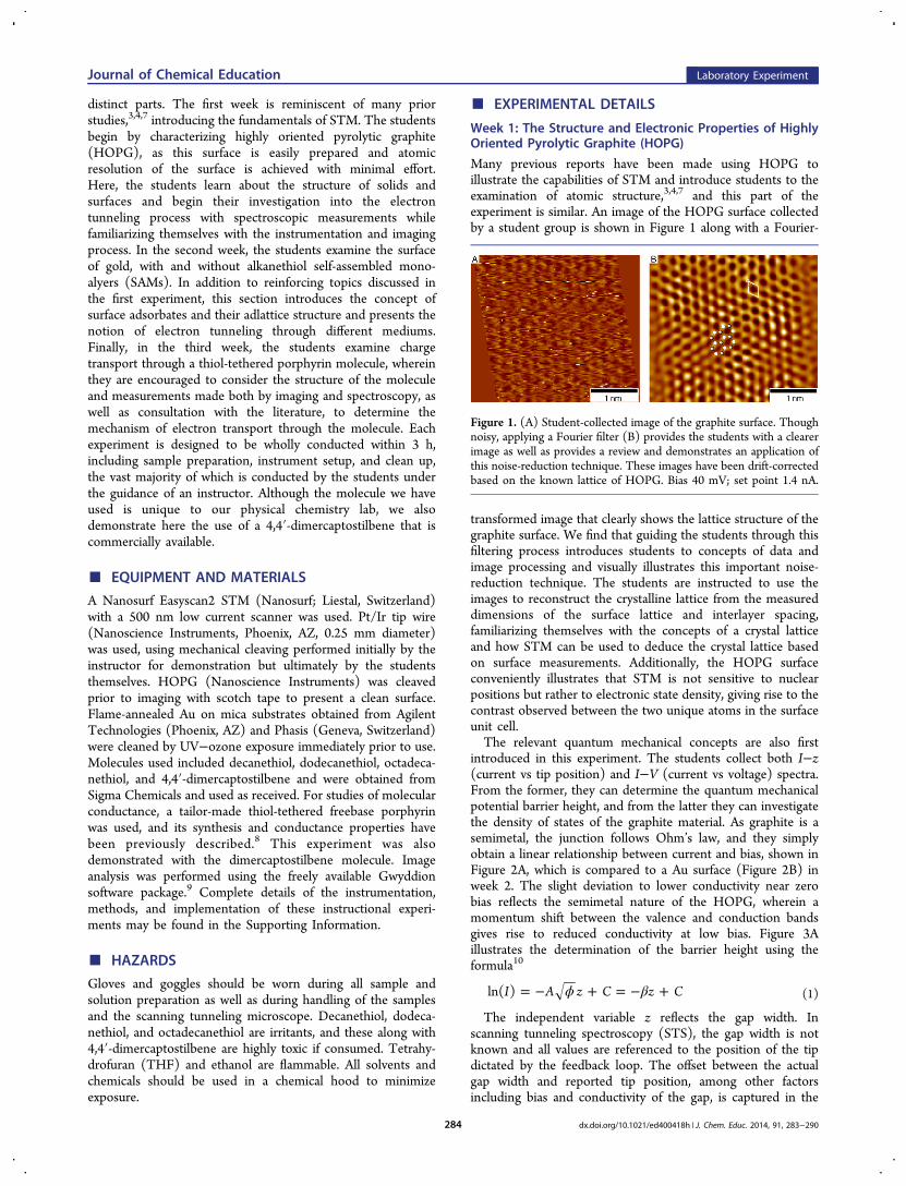
introduced in this experiment. The students collect both I−z(current vs tip position) and I−V (current vs voltage) spectra.From the former, they can determine the quantum mechanicalpotential barrier height, and from the latter they can investigatethe density of states of the graphite material. As graphite is asemimetal, the junction follows Ohm’s law, and they simplyobtain a linear relationship between current and bias, shown inFigure 2A, which is compared to a Au surface (Figure 2B) inweek 2. The slight deviation to lower conductivity near zerobias reflects the semimetal nature of the HOPG, wherein amomentum shift between the valence and conduction bandsgives rise to reduced conductivity at low bias. Figure 3Aillustrates the determination of the barrier height using theformula10
ϕ β= − + = − +I A z C z Cln( ) (1)
The independent variable z reflects the gap width. Inscanning tunneling spectroscopy (STS), the gap width is notknown and all values are referenced to the position of the tipdictated by the feedback loop. The offset between the actualgap width and reported tip position, among other factorsincluding bias and conductivity of the gap, is captured in the
Figure 1. (A) Student-collected image of the graphite surface. Thoughnoisy, applying a Fourier filter (B) provides the students with a clearerimage as well as provides a review and demonstrates an application ofthis noise-reduction technique. These images have been drift-correctedbased on the known lattice of HOPG. Bias 40 mV; set point 1.4 nA.
Journal of Chemical Education Laboratory Experiment
dx.doi.org/10.1021/ed400418h | J. Chem. Educ. 2014, 91, 283−290284
arbitrary constant C. The value A is a constant with value 1.025Å−1 when φ, the quantum mechanical potential barrier height,is given in eV.11 The more general parameter, β, termed thetunneling efficiency, can similarly be determined from the I−zspectrum as described in eq 1. This value reflects the rate ofdecay of the wave function in the tunneling region. Again, thisis compared to Au (Figure 3B) in week 2.
Week 2: Au(111) and Self-Assembled Monolayers (SAMs)on Au(111)
In week 2, the students focus their interest on adsorbed layerson a metal surface. The students are first asked to image a baregold surface. In doing so, the substrate is introduced, and topicsincluding the structure of metal crystals (fcc, bcc, and hcp)along with how different crystal faces (defined by their Millerindices) are projected as surface structures can be discussed.The basic features of the gold surface are examined, includingthe interlayer spacing of the Au(111) planes. The students areencouraged to briefly attempt to resolve the atomic structure of
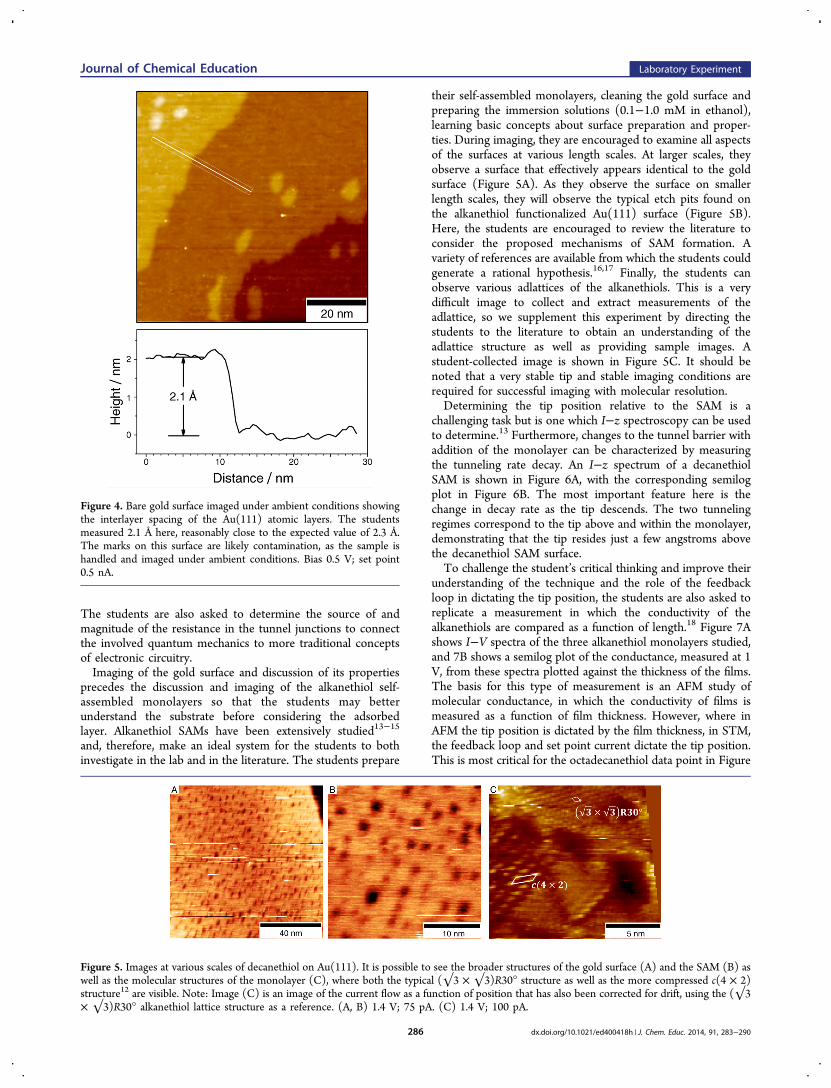
the surface; however, under ambient conditions, success ishighly unlikely. This, however, serves to further illustrate therole of the electronic structure in imaging and encourages thestudents to consider the differences in the electronic structuresof graphite and Au(111), where the more localized valenceorbitals of graphite provide greater contrast and greatereffective signalAn example of a student group’s determination of the
interlayer spacing is presented in Figure 4. The students alsoperform spectroscopy on this surface, generating both I−V andI−z spectra (Figure 2B and Figure 3B, respectively). Toreinforce the connection between the quantum mechanicalaspect of tunneling and the configuration of the experiment, thestudents are directed to compare the tunneling efficiency andbarrier height between this surface and graphite. Differences inthese measurements reflect the different imaging biasesemployed and the different work function of the materials,which together lead to changes in the effective barrier height.
Figure 2. I−V spectra of HOPG (A) and Au(111) (B) demonstrating the metallic character of these two materials. Because these materials aremetallic, Ohm’s law applies and a linear relation between current and bias is observed. The slight suppression of conductivity near 0 V in (A) isindicative of the semimetallic electronic structure of HOPG.
Figure 3. I−z spectra collected on the HOPG (A) and Au(111) (B) surface showing the I−z spectrum (black), with corresponding semilog plot(red) shown. The tunneling efficiency can be determined by a linear fit (blue), producing the tunneling efficiencies (β) and barrier heights (φ)shown. The difference in barrier height reflects the different Fermi levels of the two substrates and the different biases applied during imaging.
Journal of Chemical Education Laboratory Experiment
dx.doi.org/10.1021/ed400418h | J. Chem. Educ. 2014, 91, 283−290285
The students are also asked to determine the source of andmagnitude of the resistance in the tunnel junctions to connectthe involved quantum mechanics to more traditional conceptsof electronic circuitry.Imaging of the gold surface and discussion of its properties
precedes the discussion and imaging of the alkanethiol self-assembled monolayers so that the students may betterunderstand the substrate before considering the adsorbedlayer. Alkanethiol SAMs have been extensively studied13−15
and, therefore, make an ideal system for the students to bothinvestigate in the lab and in the literature. The students prepare
their self-assembled monolayers, cleaning the gold surface andpreparing the immersion solutions (0.1−1.0 mM in ethanol),learning basic concepts about surface preparation and proper-ties. During imaging, they are encouraged to examine all aspectsof the surfaces at various length scales. At larger scales, theyobserve a surface that effectively appears identical to the goldsurface (Figure 5A). As they observe the surface on smallerlength scales, they will observe the typical etch pits found onthe alkanethiol functionalized Au(111) surface (Figure 5B).Here, the students are encouraged to review the literature toconsider the proposed mechanisms of SAM formation. Avariety of references are available from which the students couldgenerate a rational hypothesis.16,17 Finally, the students canobserve various adlattices of the alkanethiols. This is a verydifficult image to collect and extract measurements of theadlattice, so we supplement this experiment by directing thestudents to the literature to obtain an understanding of theadlattice structure as well as providing sample images. Astudent-collected image is shown in Figure 5C. It should benoted that a very stable tip and stable imaging conditions arerequired for successful imaging with molecular resolution.Determining the tip position relative to the SAM is a
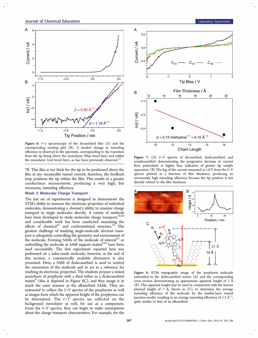
challenging task but is one which I−z spectroscopy can be usedto determine.13 Furthermore, changes to the tunnel barrier withaddition of the monolayer can be characterized by measuringthe tunneling rate decay. An I−z spectrum of a decanethiolSAM is shown in Figure 6A, with the corresponding semilogplot in Figure 6B. The most important feature here is thechange in decay rate as the tip descends. The two tunnelingregimes correspond to the tip above and within the monolayer,demonstrating that the tip resides just a few angstroms abovethe decanethiol SAM surface.To challenge the student’s critical thinking and improve their
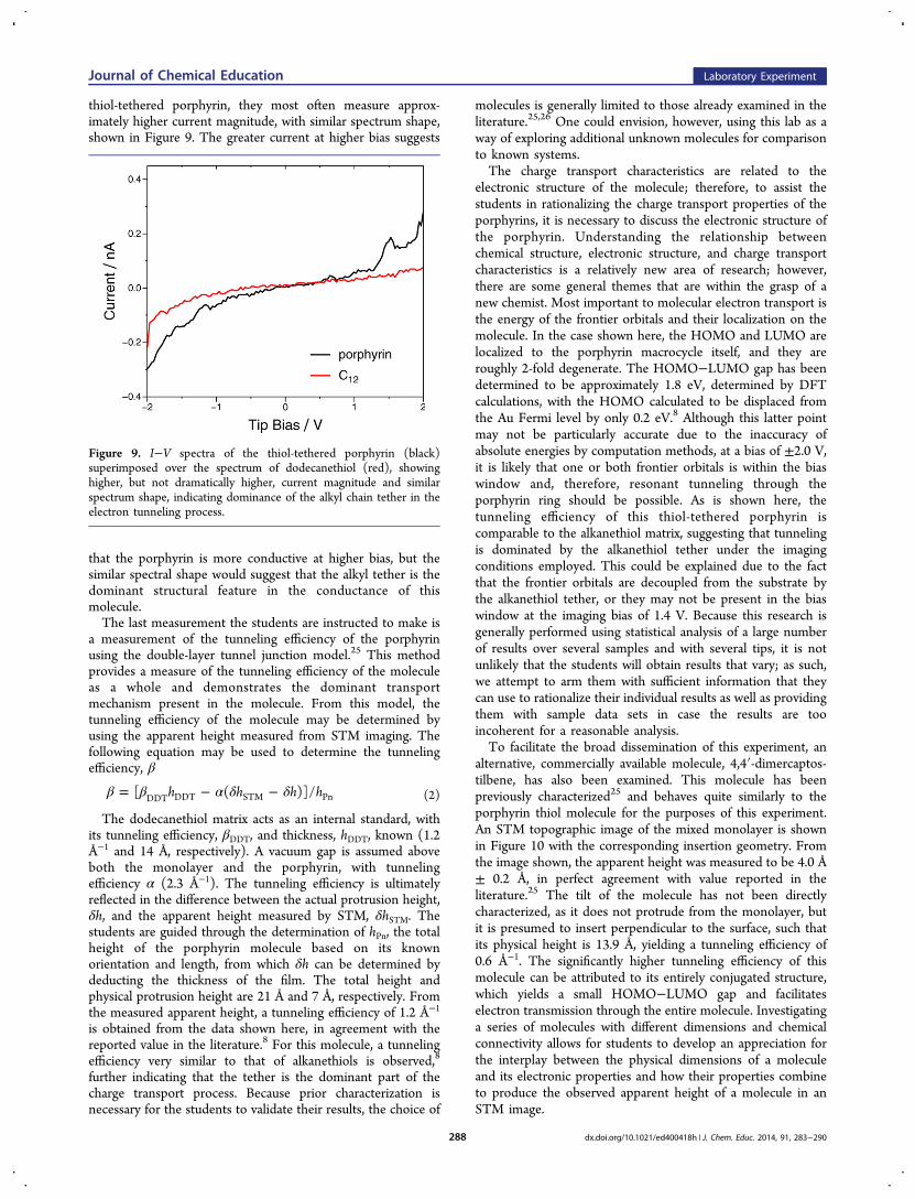
understanding of the technique and the role of the feedbackloop in dictating the tip position, the students are also asked toreplicate a measurement in which the conductivity of thealkanethiols are compared as a function of length.18 Figure 7Ashows I−V spectra of the three alkanethiol monolayers studied,and 7B shows a semilog plot of the conductance, measured at 1V, from these spectra plotted against the thickness of the films.The basis for this type of measurement is an AFM study ofmolecular conductance, in which the conductivity of films ismeasured as a function of film thickness. However, where inAFM the tip position is dictated by the film thickness, in STM,the feedback loop and set point current dictate the tip position.This is most critical for the octadecanethiol data point in Figure
Figure 4. Bare gold surface imaged under ambient conditions showingthe interlayer spacing of the Au(111) atomic layers. The studentsmeasured 2.1 Å here, reasonably close to the expected value of 2.3 Å.The marks on this surface are likely contamination, as the sample ishandled and imaged under ambient conditions. Bias 0.5 V; set point0.5 nA.
Figure 5. Images at various scales of decanethiol on Au(111). It is possible to see the broader structures of the gold surface (A) and the SAM (B) aswell as the molecular structures of the monolayer (C), where both the typical (√3 × √3)R30° structure as well as the more compressed c(4 × 2)structure12 are visible. Note: Image (C) is an image of the current flow as a function of position that has also been corrected for drift, using the (√3× √3)R30° alkanethiol lattice structure as a reference. (A, B) 1.4 V; 75 pA. (C) 1.4 V; 100 pA.
Journal of Chemical Education Laboratory Experiment
dx.doi.org/10.1021/ed400418h | J. Chem. Educ. 2014, 91, 283−290286
7B. This film is too thick for the tip to be positioned above thefilm at any measurable tunnel current; therefore, the feedbackloop positions the tip within the film. This results in a greaterconductance measurement, producing a very high, buterroneous, tunneling efficiency.Week 3: Molecular Charge Transport
The last set of experiments is designed to demonstrate theSTM’s ability to measure the electronic properties of individualmolecules, demonstrating a chemist’s ability to examine chargetransport in single molecules directly. A variety of methodshave been developed to study molecular charge transport,19,20
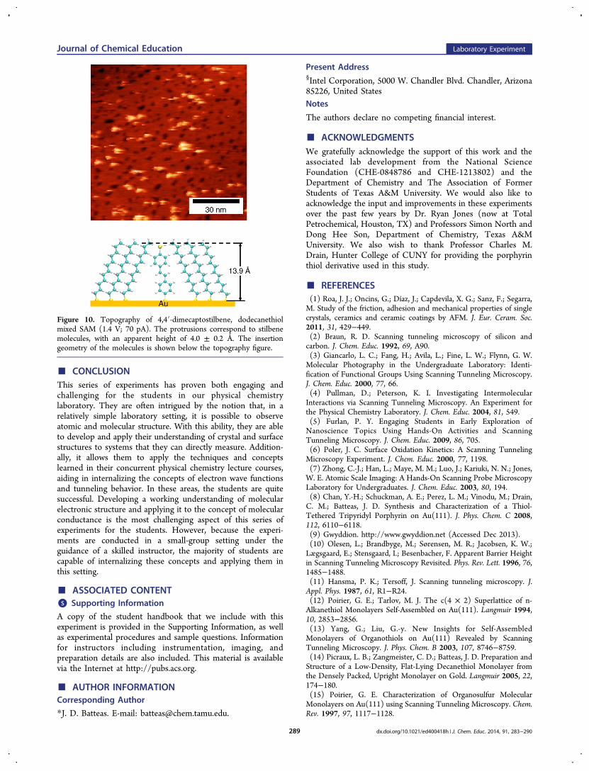
and considerable work has been conducted examining theeffects of chemical21 and conformational structure.22 Thegreatest challenge of studying single-molecule electron trans-port is adequately controlling the geometry and environment ofthe molecule. Forming SAMs of the molecule of interest23 orembedding the molecule in SAM support matrix8,24 have beenused successfully. The first experiment reported here wasperformed on a tailor-made molecule; however, at the end ofthis section, a commercially available alternative is alsopresented. Here, a SAM of dodecanethiol is used to controlthe orientation of the molecule and to act as a reference forstudying its electronic properties. The students prepare a mixedmonolayer of porphyrin with a thiol tether in a dodecanethiolmatrix8 (this is depicted in Figure 8C), and they image it inmuch the same manner as the alkanethiol SAMs. They areinstructed to collect the I−V spectra of the porphyrins as wellas images from which the apparent height of the porphyrins canbe determined. The I−V spectra are collected on thebackground monolayer as well, for use as a comparison.From the I−V spectra, they can begin to make assumptionsabout the charge transport characteristics. For example, for the
Figure 6. I−z spectroscopy of the decanethiol film (A) and thecorresponding semilog plot (B). A modest change in tunnelingefficiency is observed in the spectrum, corresponding to the transitionfrom the tip being above the monolayer (blue trend line) and withinthe monolayer (red trend line), as has been previously observed.13
Figure 7. (A) I−V spectra of decanethiol, dodecanethiol, andoctadecanethiol demonstrating the progressive decrease in currentflow, particularly at higher bias, indicative of greater tip sampleseparation. (B) The log of the current measured at 1.0 V from the I−Vspectra plotted as a function of film thickness, producing anerroneously high tunneling efficiency because the tip position is notdirectly related to the film thickness.
Figure 8. STM topographic image of the porphyrin moleculeembedded in the dodecanethiol matrix (A) and the correspondingcross section demonstrating an approximate apparent height of 3 Å(B). This apparent height may be used in conjunction with the knownphysical height of 7 Å, shown in (C), to determine the averagetunneling efficiency of the molecule by the double-layer tunneljunction model, resulting in an average tunneling efficiency of 1.2 Å−1,quite similar to that of an alkanethiol.
Journal of Chemical Education Laboratory Experiment
dx.doi.org/10.1021/ed400418h | J. Chem. Educ. 2014, 91, 283−290287
thiol-tethered porphyrin, they most often measure approx-imately higher current magnitude, with similar spectrum shape,shown in Figure 9. The greater current at higher bias suggests
that the porphyrin is more conductive at higher bias, but thesimilar spectral shape would suggest that the alkyl tether is thedominant structural feature in the conductance of thismolecule.The last measurement the students are instructed to make is
a measurement of the tunneling efficiency of the porphyrinusing the double-layer tunnel junction model.25 This methodprovides a measure of the tunneling efficiency of the moleculeas a whole and demonstrates the dominant transportmechanism present in the molecule. From this model, thetunneling efficiency of the molecule may be determined byusing the apparent height measured from STM imaging. Thefollowing equation may be used to determine the tunnelingefficiency, β
β β α δ δ= − −h h h h[ ( )]/DDT DDT STM Pn (2)
The dodecanethiol matrix acts as an internal standard, withits tunneling efficiency, βDDT, and thickness, hDDT, known (1.2Å−1 and 14 Å, respectively). A vacuum gap is assumed aboveboth the monolayer and the porphyrin, with tunnelingefficiency α (2.3 Å−1). The tunneling efficiency is ultimatelyreflected in the difference between the actual protrusion height,δh, and the apparent height measured by STM, δhSTM. Thestudents are guided through the determination of hPn, the totalheight of the porphyrin molecule based on its knownorientation and length, from which δh can be determined bydeducting the thickness of the film. The total height andphysical protrusion height are 21 Å and 7 Å, respectively. Fromthe measured apparent height, a tunneling efficiency of 1.2 Å−1
is obtained from the data shown here, in agreement with thereported value in the literature.8 For this molecule, a tunnelingefficiency very similar to that of alkanethiols is observed,8
further indicating that the tether is the dominant part of thecharge transport process. Because prior characterization isnecessary for the students to validate their results, the choice of
molecules is generally limited to those already examined in theliterature.25,26 One could envision, however, using this lab as away of exploring additional unknown molecules for comparisonto known systems.The charge transport characteristics are related to the
electronic structure of the molecule; therefore, to assist thestudents in rationalizing the charge transport properties of theporphyrins, it is necessary to discuss the electronic structure ofthe porphyrin. Understanding the relationship betweenchemical structure, electronic structure, and charge transportcharacteristics is a relatively new area of research; however,there are some general themes that are within the grasp of anew chemist. Most important to molecular electron transport isthe energy of the frontier orbitals and their localization on themolecule. In the case shown here, the HOMO and LUMO arelocalized to the porphyrin macrocycle itself, and they areroughly 2-fold degenerate. The HOMO−LUMO gap has beendetermined to be approximately 1.8 eV, determined by DFTcalculations, with the HOMO calculated to be displaced fromthe Au Fermi level by only 0.2 eV.8 Although this latter pointmay not be particularly accurate due to the inaccuracy ofabsolute energies by computation methods, at a bias of ±2.0 V,it is likely that one or both frontier orbitals is within the biaswindow and, therefore, resonant tunneling through theporphyrin ring should be possible. As is shown here, thetunneling efficiency of this thiol-tethered porphyrin iscomparable to the alkanethiol matrix, suggesting that tunnelingis dominated by the alkanethiol tether under the imagingconditions employed. This could be explained due to the factthat the frontier orbitals are decoupled from the substrate bythe alkanethiol tether, or they may not be present in the biaswindow at the imaging bias of 1.4 V. Because this research isgenerally performed using statistical analysis of a large numberof results over several samples and with several tips, it is notunlikely that the students will obtain results that vary; as such,we attempt to arm them with sufficient information that theycan use to rationalize their individual results as well as providingthem with sample data sets in case the results are tooincoherent for a reasonable analysis.To facilitate the broad dissemination of this experiment, an
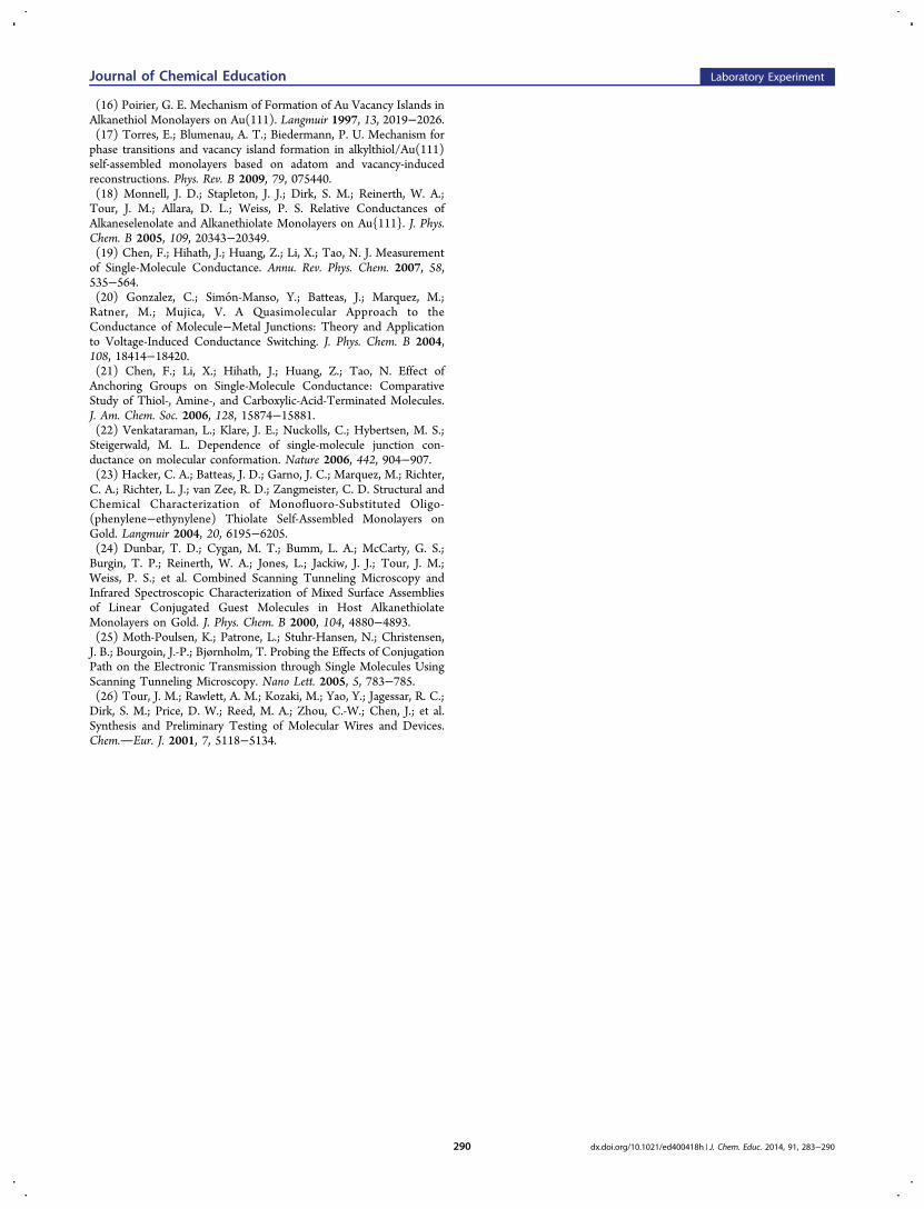
alternative, commercially available molecule, 4,4′-dimercaptos-tilbene, has also been examined. This molecule has beenpreviously characterized25 and behaves quite similarly to theporphyrin thiol molecule for the purposes of this experiment.An STM topographic image of the mixed monolayer is shownin Figure 10 with the corresponding insertion geometry. Fromthe image shown, the apparent height was measured to be 4.0 ű 0.2 Å, in perfect agreement with value reported in theliterature.25 The tilt of the molecule has not been directlycharacterized, as it does not protrude from the monolayer, butit is presumed to insert perpendicular to the surface, such thatits physical height is 13.9 Å, yielding a tunneling efficiency of0.6 Å−1. The significantly higher tunneling efficiency of thismolecule can be attributed to its entirely conjugated structure,which yields a small HOMO−LUMO gap and facilitateselectron transmission through the entire molecule. Investigatinga series of molecules with different dimensions and chemicalconnectivity allows for students to develop an appreciation forthe interplay between the physical dimensions of a moleculeand its electronic properties and how their properties combineto produce the observed apparent height of a molecule in anSTM image.
Figure 9. I−V spectra of the thiol-tethered porphyrin (black)superimposed over the spectrum of dodecanethiol (red), showinghigher, but not dramatically higher, current magnitude and similarspectrum shape, indicating dominance of the alkyl chain tether in theelectron tunneling process.
Journal of Chemical Education Laboratory Experiment
dx.doi.org/10.1021/ed400418h | J. Chem. Educ. 2014, 91, 283−290288
■ CONCLUSIONThis series of experiments has proven both engaging andchallenging for the students in our physical chemistrylaboratory. They are often intrigued by the notion that, in arelatively simple laboratory setting, it is possible to observeatomic and molecular structure. With this ability, they are ableto develop and apply their understanding of crystal and surfacestructures to systems that they can directly measure. Addition-ally, it allows them to apply the techniques and conceptslearned in their concurrent physical chemistry lecture courses,aiding in internalizing the concepts of electron wave functionsand tunneling behavior. In these areas, the students are quitesuccessful. Developing a working understanding of molecularelectronic structure and applying it to the concept of molecularconductance is the most challenging aspect of this series ofexperiments for the students. However, because the experi-ments are conducted in a small-group setting under theguidance of a skilled instructor, the majority of students arecapable of internalizing these concepts and applying them inthis setting.
■ ASSOCIATED CONTENT*S Supporting Information
A copy of the student handbook that we include with thisexperiment is provided in the Supporting Information, as wellas experimental procedures and sample questions. Informationfor instructors including instrumentation, imaging, andpreparation details are also included. This material is availablevia the Internet at http://pubs.acs.org.
■ AUTHOR INFORMATIONCorresponding Author
*J. D. Batteas. E-mail: [email protected].
Present Address§Intel Corporation, 5000 W. Chandler Blvd. Chandler, Arizona85226, United StatesNotes
The authors declare no competing financial interest.
■ ACKNOWLEDGMENTSWe gratefully acknowledge the support of this work and theassociated lab development from the National ScienceFoundation (CHE-0848786 and CHE-1213802) and theDepartment of Chemistry and The Association of FormerStudents of Texas A&M University. We would also like toacknowledge the input and improvements in these experimentsover the past few years by Dr. Ryan Jones (now at TotalPetrochemical, Houston, TX) and Professors Simon North andDong Hee Son, Department of Chemistry, Texas A&MUniversity. We also wish to thank Professor Charles M.Drain, Hunter College of CUNY for providing the porphyrinthiol derivative used in this study.
■ REFERENCES(1) Roa, J. J.; Oncins, G.; Díaz, J.; Capdevila, X. G.; Sanz, F.; Segarra,M. Study of the friction, adhesion and mechanical properties of singlecrystals, ceramics and ceramic coatings by AFM. J. Eur. Ceram. Soc.2011, 31, 429−449.(2) Braun, R. D. Scanning tunneling microscopy of silicon andcarbon. J. Chem. Educ. 1992, 69, A90.(3) Giancarlo, L. C.; Fang, H.; Avila, L.; Fine, L. W.; Flynn, G. W.Molecular Photography in the Undergraduate Laboratory: Identi-fication of Functional Groups Using Scanning Tunneling Microscopy.J. Chem. Educ. 2000, 77, 66.(4) Pullman, D.; Peterson, K. I. Investigating IntermolecularInteractions via Scanning Tunneling Microscopy. An Experiment forthe Physical Chemistry Laboratory. J. Chem. Educ. 2004, 81, 549.(5) Furlan, P. Y. Engaging Students in Early Exploration ofNanoscience Topics Using Hands-On Activities and ScanningTunneling Microscopy. J. Chem. Educ. 2009, 86, 705.(6) Poler, J. C. Surface Oxidation Kinetics: A Scanning TunnelingMicroscopy Experiment. J. Chem. Educ. 2000, 77, 1198.(7) Zhong, C.-J.; Han, L.; Maye, M. M.; Luo, J.; Kariuki, N. N.; Jones,W. E. Atomic Scale Imaging: A Hands-On Scanning Probe MicroscopyLaboratory for Undergraduates. J. Chem. Educ. 2003, 80, 194.(8) Chan, Y.-H.; Schuckman, A. E.; Perez, L. M.; Vinodu, M.; Drain,C. M.; Batteas, J. D. Synthesis and Characterization of a Thiol-Tethered Tripyridyl Porphyrin on Au(111). J. Phys. Chem. C 2008,112, 6110−6118.(9) Gwyddion. http://www.gwyddion.net (Accessed Dec 2013).(10) Olesen, L.; Brandbyge, M.; Sørensen, M. R.; Jacobsen, K. W.;Lægsgaard, E.; Stensgaard, I.; Besenbacher, F. Apparent Barrier Heightin Scanning Tunneling Microscopy Revisited. Phys. Rev. Lett. 1996, 76,1485−1488.(11) Hansma, P. K.; Tersoff, J. Scanning tunneling microscopy. J.Appl. Phys. 1987, 61, R1−R24.(12) Poirier, G. E.; Tarlov, M. J. The c(4 × 2) Superlattice of n-Alkanethiol Monolayers Self-Assembled on Au(111). Langmuir 1994,10, 2853−2856.(13) Yang, G.; Liu, G.-y. New Insights for Self-AssembledMonolayers of Organothiols on Au(111) Revealed by ScanningTunneling Microscopy. J. Phys. Chem. B 2003, 107, 8746−8759.(14) Picraux, L. B.; Zangmeister, C. D.; Batteas, J. D. Preparation andStructure of a Low-Density, Flat-Lying Decanethiol Monolayer fromthe Densely Packed, Upright Monolayer on Gold. Langmuir 2005, 22,174−180.(15) Poirier, G. E. Characterization of Organosulfur MolecularMonolayers on Au(111) using Scanning Tunneling Microscopy. Chem.Rev. 1997, 97, 1117−1128.
Figure 10. Topography of 4,4′-dimecaptostilbene, dodecanethiolmixed SAM (1.4 V; 70 pA). The protrusions correspond to stilbenemolecules, with an apparent height of 4.0 ± 0.2 Å. The insertiongeometry of the molecules is shown below the topography figure.
Journal of Chemical Education Laboratory Experiment
dx.doi.org/10.1021/ed400418h | J. Chem. Educ. 2014, 91, 283−290289
(16) Poirier, G. E. Mechanism of Formation of Au Vacancy Islands inAlkanethiol Monolayers on Au(111). Langmuir 1997, 13, 2019−2026.(17) Torres, E.; Blumenau, A. T.; Biedermann, P. U. Mechanism forphase transitions and vacancy island formation in alkylthiol/Au(111)self-assembled monolayers based on adatom and vacancy-inducedreconstructions. Phys. Rev. B 2009, 79, 075440.(18) Monnell, J. D.; Stapleton, J. J.; Dirk, S. M.; Reinerth, W. A.;Tour, J. M.; Allara, D. L.; Weiss, P. S. Relative Conductances ofAlkaneselenolate and Alkanethiolate Monolayers on Au{111}. J. Phys.Chem. B 2005, 109, 20343−20349.(19) Chen, F.; Hihath, J.; Huang, Z.; Li, X.; Tao, N. J. Measurementof Single-Molecule Conductance. Annu. Rev. Phys. Chem. 2007, 58,535−564.(20) Gonzalez, C.; Simon-Manso, Y.; Batteas, J.; Marquez, M.;Ratner, M.; Mujica, V. A Quasimolecular Approach to theConductance of Molecule−Metal Junctions: Theory and Applicationto Voltage-Induced Conductance Switching. J. Phys. Chem. B 2004,108, 18414−18420.(21) Chen, F.; Li, X.; Hihath, J.; Huang, Z.; Tao, N. Effect ofAnchoring Groups on Single-Molecule Conductance: ComparativeStudy of Thiol-, Amine-, and Carboxylic-Acid-Terminated Molecules.J. Am. Chem. Soc. 2006, 128, 15874−15881.(22) Venkataraman, L.; Klare, J. E.; Nuckolls, C.; Hybertsen, M. S.;Steigerwald, M. L. Dependence of single-molecule junction con-ductance on molecular conformation. Nature 2006, 442, 904−907.(23) Hacker, C. A.; Batteas, J. D.; Garno, J. C.; Marquez, M.; Richter,C. A.; Richter, L. J.; van Zee, R. D.; Zangmeister, C. D. Structural andChemical Characterization of Monofluoro-Substituted Oligo-(phenylene−ethynylene) Thiolate Self-Assembled Monolayers onGold. Langmuir 2004, 20, 6195−6205.(24) Dunbar, T. D.; Cygan, M. T.; Bumm, L. A.; McCarty, G. S.;Burgin, T. P.; Reinerth, W. A.; Jones, L.; Jackiw, J. J.; Tour, J. M.;Weiss, P. S.; et al. Combined Scanning Tunneling Microscopy andInfrared Spectroscopic Characterization of Mixed Surface Assembliesof Linear Conjugated Guest Molecules in Host AlkanethiolateMonolayers on Gold. J. Phys. Chem. B 2000, 104, 4880−4893.(25) Moth-Poulsen, K.; Patrone, L.; Stuhr-Hansen, N.; Christensen,J. B.; Bourgoin, J.-P.; Bjørnholm, T. Probing the Effects of ConjugationPath on the Electronic Transmission through Single Molecules UsingScanning Tunneling Microscopy. Nano Lett. 2005, 5, 783−785.(26) Tour, J. M.; Rawlett, A. M.; Kozaki, M.; Yao, Y.; Jagessar, R. C.;Dirk, S. M.; Price, D. W.; Reed, M. A.; Zhou, C.-W.; Chen, J.; et al.Synthesis and Preliminary Testing of Molecular Wires and Devices.Chem.Eur. J. 2001, 7, 5118−5134.
Journal of Chemical Education Laboratory Experiment
dx.doi.org/10.1021/ed400418h | J. Chem. Educ. 2014, 91, 283−290290