Embed Size (px)
Citation preview

Wide Band Gap Semiconductor Based Highpower ATT Diodes In The MM-wave and THz Regime: Device Reliability, Experimental Feasibility and Photo-sensitivity 113
Wide Band Gap Semiconductor Based Highpower ATT Diodes In The MM-wave and THz Regime: Device Reliability, Experimental Feasibility and Photo-sensitivity
Moumita Mukherjee
X
Wide Band Gap Semiconductor Based High-power ATT Diodes In The MM-wave and THz
Regime: Device Reliability, Experimental Feasibility and Photo-sensitivity
Moumita Mukherjee
Centre of MM-Wave Semiconductor Devices & Systems(CMSDS), Centre of Advanced Study in Radio Physics & Electronics, University of Calcutta,
INDIA
1. Introduction
Avalanche Transit Time (ATT) Diodes which include IMPATTs, TRAPATTs, BARITTs and so on are potential solid-state sources for Microwave power. Among these devices, IMPATTs are by far the most important in view of their frequency range and power output and show great promise of increasing application in the twenty first century. During the initial phases of development of IMPATT devices in the late sixties and early seventies, Ge (Germanium) and Si (Silicon) were mainly used as semiconducting materials for IMPATT fabrication. In view of their low power capability, Ge IMPATTs have now become obsolete. In the seventies the rapid development of Si technology has made possible the emergence of Si SDR and DDR IMPATTs which can provide power at microwave and MM-wave frequency bands. GaAs (Gallium Arsenide) also emerged as a highly suitable material for fabricating IMPATT diodes in the lower microwave frequency range. Now-a-days IMPATT devices are used in microwave and MM-wave digital and analog communication systems, high power RADARs, missile seekers, and in many other defence systems. In recent years, the development of sources for Terahertz frequency regime are being extensively explored worldwide, for applications in short-range terrestrial and airborne communications, spectroscopy, imaging, space-based communications and atmospheric sensing. To meet the rising demand of high-power, high-frequency solid-state sources, extensive research is being carried out for development of high-power IMPATT devices in MM-wave and Terahertz regime. The material parameters responsible for heat generation and dissipation in IMPATT diodes play a vital role in limiting the output power of conventional Si and GaAs IMPATT diodes at a particular frequency. Among several approaches for realizing high-power, high-frequency IMPATT sources, one option is to develop IMPATT devices based on Wide-Band-Gap (WBG) semiconductors (e.g. SiC and GaN) having high critical electric field (EC), high carrier saturation velocity (vS) as well as high thermal conductivity (K) (Table 1) [Trew et al.], since RF power output from an
7
www.intechopen.com

Advanced Microwave and Millimeter Wave Technologies: Semiconductor Devices, Circuits and Systems114
IMPATT is proportional to EC2 vs2. Moreover, high value of K is essential to ensure good thermal stability for high-power operation of the devices. All these intrinsic material parameters of WBG semiconductors are favorable for realizing smaller transit time, an essential criterion for developing THz devices. The expected excellent performances of WBG devices can also be expressed by figures of merit (FOM).
Table 1. Material properties of Si, GaAs, InP and important Wide Bandgap semiconductors. The Baliga FOM is important for evaluation of high frequency application and Johnson’s FOM considers the high-frequency and high-power capability of devices. Taking Baliga and Johnson’s FOM for Si as unity, the Baliga and Johnson’s FOM for GaAs are 11.0 and 7.1, respectively, while those for WBG semiconductor SiC are 29.0 and 278 and those for GaN are 77.8 and 756. Hence, SiC and GaN are found to be superior to both conventional Si and GaAs for high-frequency and high-power operation. Thus, in a bid to find single small-sized MM-wave and THz power sources, it is interesting to study the prospects of WBG semiconductor based IMPATT diodes.
Semiconductor
Si GaAs 6H-SiC 4H-SiC 3C-SiC
WZ-GaN
ZB-GaN
InP Diamond
Bandgap (Eg) (eV)
1.12 1.43 3.03 3.26 2.2 3.45 3.28 1.35 5.45
Critical Electric Breakdown field (EC) (107 V.m-1)
3.0 4.0 25.0 ( to c-axis)
22.0 ( to c-axis)
21.2 20.0 20.0 5.0 100.0
Relative dielectric constant (€r)
11.9 13.1 9.66 9.7 9.7 8.9 9.7 12.5 5.5
Electron mobility (µn) (m2 V-1s-1)
0.15 0.85 0.04 ( to c-axis) 0.05 ( to c- axis)
0.10 (both and to c- axis)
0.075
0.125 0.100 0.54 0.22
Hole mobility (µp) (m2 V-1s-1)
0.06 0.04 0.01 0.01 0.004 0.085 0.035 0.02 0.085
Saturated carrier drift velocity (vs) ( to c-axis) (105 ms-1)
1.0 1.2 2.0 2.0 2.2 2.5 2.0 2.2 2.7
Thermal Conductivity (K) (Wm-1 K-1)
150.0 46.0 490.0 490.0 320.0 225.0 130.0 69.0 2200.0
In this Chapter, the DC and high-frequency characteristics of SiC and GaN based IMPATT devices at MM-wave and THz region will be presented first. This will be followed by the photo-sensitivity and experimental feasibility studies of the new-class of IMPATT devices.
2. IMPATT diode: brief history of development.
IMPATT is an acronym of IMPact ionization Avalanche Transit Time, which reflects the mechanism of its operation. In its simplest form, an IMPATT is a p-n junction diode reversed biased to breakdown, in which an avalanche of electron-hole pair is produced in the high-field region of the device depletion layer by ‘impact ionization’. The transit of the carriers through the depletion layer leads to generation of microwave and MM-waves when the device is tuned in a suitable microwave and MM-wave cavity. These diodes exhibit negative resistance at microwave and MM-wave frequencies due to two electronic delays, viz., (i) ‘avalanche build-up delay’ due to ‘impact ionization’ leading to avalanche multiplication of charge carriers and (ii) ‘transit time delay’ due to the saturation of drift velocity of charge carriers moving under the influence of a high electric field. The working principles of the device were first described by Read in 1958. However, the idea of obtaining a negative resistance from a reversed biased p-n junction dates back to an earlier paper (1954) by Shockley, in which he showed that when an electron bunch from a forward biased cathode is injected into the depletion layer of a reversed biased p-n junction a ‘transit time negative resistance’ is produced as the electrons drift across the high field region. The negative resistance from such early devices was found to be small and microwave power output was low. Read showed that an improved negative resistance is obtained when impact ionization is used to inject the electrons. He showed that the properties of charge carriers in a semiconductor i.e. (i) avalanche multiplication by impact ionization and (ii) transit time delay of charge carriers due to saturation of drift velocity at high electric fields, could be suitably combined in a reverse-biased p-n junction to produce a microwave negative resistance. By exploiting the time delay required to build up an avalanche discharge by impact ionization, coupled with Shockley’s transit time delay, he showed that efficient microwave oscillation could be realized in his proposed p+ n i n+ diode. However, due to the complicated nature of the Read structure, it was not until 1965 that the first experimental Read diode was fabricated. In the early 1965 Johnston et al., from Bell Laboratories, first made a successful experimental observation of microwave oscillations from a simple Si p-n junction diode. This study showed that the complicated Read structure was not essential required for generating microwave oscillations. On the basis of a small-signal analysis, T. Misawa showed that negative resistance would occur in a reverse biased p-n junction of any arbitrary doping profile. Since then, rapid advances have been made towards further development of various IMPATT structures, fabrication techniques as well as optimum circuit design for IMPATT oscillators and amplifiers. The frequency range of IMPATT devices can be pushed easily to MM and sub-MM wave ranges at which comparable amount of RF power generation is hardly possible by other two-terminal solid-state devices.
www.intechopen.com

Wide Band Gap Semiconductor Based Highpower ATT Diodes In The MM-wave and THz Regime: Device Reliability, Experimental Feasibility and Photo-sensitivity 115
IMPATT is proportional to EC2 vs2. Moreover, high value of K is essential to ensure good thermal stability for high-power operation of the devices. All these intrinsic material parameters of WBG semiconductors are favorable for realizing smaller transit time, an essential criterion for developing THz devices. The expected excellent performances of WBG devices can also be expressed by figures of merit (FOM).
Table 1. Material properties of Si, GaAs, InP and important Wide Bandgap semiconductors. The Baliga FOM is important for evaluation of high frequency application and Johnson’s FOM considers the high-frequency and high-power capability of devices. Taking Baliga and Johnson’s FOM for Si as unity, the Baliga and Johnson’s FOM for GaAs are 11.0 and 7.1, respectively, while those for WBG semiconductor SiC are 29.0 and 278 and those for GaN are 77.8 and 756. Hence, SiC and GaN are found to be superior to both conventional Si and GaAs for high-frequency and high-power operation. Thus, in a bid to find single small-sized MM-wave and THz power sources, it is interesting to study the prospects of WBG semiconductor based IMPATT diodes.
Semiconductor
Si GaAs 6H-SiC 4H-SiC 3C-SiC
WZ-GaN
ZB-GaN
InP Diamond
Bandgap (Eg) (eV)
1.12 1.43 3.03 3.26 2.2 3.45 3.28 1.35 5.45
Critical Electric Breakdown field (EC) (107 V.m-1)
3.0 4.0 25.0 ( to c-axis)
22.0 ( to c-axis)
21.2 20.0 20.0 5.0 100.0
Relative dielectric constant (€r)
11.9 13.1 9.66 9.7 9.7 8.9 9.7 12.5 5.5
Electron mobility (µn) (m2 V-1s-1)
0.15 0.85 0.04 ( to c-axis) 0.05 ( to c- axis)
0.10 (both and to c- axis)
0.075
0.125 0.100 0.54 0.22
Hole mobility (µp) (m2 V-1s-1)
0.06 0.04 0.01 0.01 0.004 0.085 0.035 0.02 0.085
Saturated carrier drift velocity (vs) ( to c-axis) (105 ms-1)
1.0 1.2 2.0 2.0 2.2 2.5 2.0 2.2 2.7
Thermal Conductivity (K) (Wm-1 K-1)
150.0 46.0 490.0 490.0 320.0 225.0 130.0 69.0 2200.0
In this Chapter, the DC and high-frequency characteristics of SiC and GaN based IMPATT devices at MM-wave and THz region will be presented first. This will be followed by the photo-sensitivity and experimental feasibility studies of the new-class of IMPATT devices.
2. IMPATT diode: brief history of development.
IMPATT is an acronym of IMPact ionization Avalanche Transit Time, which reflects the mechanism of its operation. In its simplest form, an IMPATT is a p-n junction diode reversed biased to breakdown, in which an avalanche of electron-hole pair is produced in the high-field region of the device depletion layer by ‘impact ionization’. The transit of the carriers through the depletion layer leads to generation of microwave and MM-waves when the device is tuned in a suitable microwave and MM-wave cavity. These diodes exhibit negative resistance at microwave and MM-wave frequencies due to two electronic delays, viz., (i) ‘avalanche build-up delay’ due to ‘impact ionization’ leading to avalanche multiplication of charge carriers and (ii) ‘transit time delay’ due to the saturation of drift velocity of charge carriers moving under the influence of a high electric field. The working principles of the device were first described by Read in 1958. However, the idea of obtaining a negative resistance from a reversed biased p-n junction dates back to an earlier paper (1954) by Shockley, in which he showed that when an electron bunch from a forward biased cathode is injected into the depletion layer of a reversed biased p-n junction a ‘transit time negative resistance’ is produced as the electrons drift across the high field region. The negative resistance from such early devices was found to be small and microwave power output was low. Read showed that an improved negative resistance is obtained when impact ionization is used to inject the electrons. He showed that the properties of charge carriers in a semiconductor i.e. (i) avalanche multiplication by impact ionization and (ii) transit time delay of charge carriers due to saturation of drift velocity at high electric fields, could be suitably combined in a reverse-biased p-n junction to produce a microwave negative resistance. By exploiting the time delay required to build up an avalanche discharge by impact ionization, coupled with Shockley’s transit time delay, he showed that efficient microwave oscillation could be realized in his proposed p+ n i n+ diode. However, due to the complicated nature of the Read structure, it was not until 1965 that the first experimental Read diode was fabricated. In the early 1965 Johnston et al., from Bell Laboratories, first made a successful experimental observation of microwave oscillations from a simple Si p-n junction diode. This study showed that the complicated Read structure was not essential required for generating microwave oscillations. On the basis of a small-signal analysis, T. Misawa showed that negative resistance would occur in a reverse biased p-n junction of any arbitrary doping profile. Since then, rapid advances have been made towards further development of various IMPATT structures, fabrication techniques as well as optimum circuit design for IMPATT oscillators and amplifiers. The frequency range of IMPATT devices can be pushed easily to MM and sub-MM wave ranges at which comparable amount of RF power generation is hardly possible by other two-terminal solid-state devices.
www.intechopen.com

Advanced Microwave and Millimeter Wave Technologies: Semiconductor Devices, Circuits and Systems116
3. IMPATT structures and doping profiles
The typical doping profile of a Read diode makes its realization very difficult in practice. There are several other structures with simpler doping profiles which also exhibits microwave negative resistance due to IMPATT action. In practically realizable structures, the avalanche region is not very thin as was in case of Read diode and also there is no distinct demarcation between avalanche and drift regions. Single Drift Region (SDR) and Double Drift Region (DDR) IMPATTs are now commonly used belong to this category. Single drift IMPATT (SDR) structure is based on a one-sided abrupt p-n junction of the form p+ n n+ or n+ p p+. These diodes have a single avalanche zone of finite width located at one end of the depletion layer near the junction followed by a single drift region. The doping profile at the junction and at the interface of substrate and epitaxy are approximated by use of appropriate exponential and error function. The schematic doping profile of a typical SDR diode is shown in Figure 1. Conventional SDR diodes are fabricated with Si and GaAs as base semiconductor material. SDR p+ n n+ IMPATT structure is better than n+ p p+ structure because technology of n+ substrate is more advanced and better understood than p+ substrate. Further, the extent of the un-depleted region between the edge of the depletion region and interface of epitaxy and substrate (un-swept epitaxy), which contributes positive series resistance and thereby dissipates microwave power, is smaller in p+ n n+ structure than complimentary n+ p p+ structure, since, compared to hole mobility, mobility of electrons in most of the semiconductors are much larger owing to its lower effective mass. The fabrication of GaAs and InP SDR IMPATTs has been mostly reported with p+ n n+ structure because of the advantages of better avalanche characteristics, lower loss due to un-swept epitaxy and advanced n+ substrate technology. Double Drift IMPATT diode is another type of structure. A DDR diode is basically a p+ p n n+ (or its complementary) multilayer structure usually with a symmetrical step junction. A typical flat profile DDR along with its schematic doping profile and E(x) profile are shown in Figure 2. The E(x) profile is characterized by a centrally located high field (> 107 Vm-1) around the metallurgical junction along with two low field drift regions, for electrons and holes, on either side. The holes generated in the avalanche region drift through the drift region on the p-side while the generated electrons drift through the drift region on the n-side. In comparison to the SDR structure, in case of the DDR structure contribution to microwave power comes from the two drift regions. The second drift region in the DDR diode, improves the efficiency, RF power density and impedance per unit area. The impedance of an IMPATT diode can be approximated by a simple equivalent circuit which consists of a series combination of negative resistance (RD) and reactance (XD). In the oscillating frequency range, the magnitude of RD < XD, and thus the device reactance is approximately that of the capacitance formed by the depletion layer of the device. In the DDR structure, the added drift region increases the depletion layer width resulting in a smaller capacitance and hence a large reactance per unit area. Thus, the impedance level of a DDR diode is high as compared to that of the SDR diode. Several workers have previously suggested that the efficiency and RF power output of SDR or DDR diodes can be enhanced by modifying the epi-layer doping profile. The introduction of an impurity bump i.e. the region of high doping density, considerably improves the device efficiency. Impurity bumps can be suitably introduced in the depletion region by Molecular Beam Epitaxy (MBE) or by ion implantation to produce high-efficieny IMPATT diodes.
Fig. 1. Schematic diode structure, electric field and droping profiles of n++ pp++ and p++ n+
SDR diodes
Fig. 2. The schematic diode structure, doping profile and field profile of a Double Drift flat profile diode
www.intechopen.com

Wide Band Gap Semiconductor Based Highpower ATT Diodes In The MM-wave and THz Regime: Device Reliability, Experimental Feasibility and Photo-sensitivity 117
3. IMPATT structures and doping profiles
The typical doping profile of a Read diode makes its realization very difficult in practice. There are several other structures with simpler doping profiles which also exhibits microwave negative resistance due to IMPATT action. In practically realizable structures, the avalanche region is not very thin as was in case of Read diode and also there is no distinct demarcation between avalanche and drift regions. Single Drift Region (SDR) and Double Drift Region (DDR) IMPATTs are now commonly used belong to this category. Single drift IMPATT (SDR) structure is based on a one-sided abrupt p-n junction of the form p+ n n+ or n+ p p+. These diodes have a single avalanche zone of finite width located at one end of the depletion layer near the junction followed by a single drift region. The doping profile at the junction and at the interface of substrate and epitaxy are approximated by use of appropriate exponential and error function. The schematic doping profile of a typical SDR diode is shown in Figure 1. Conventional SDR diodes are fabricated with Si and GaAs as base semiconductor material. SDR p+ n n+ IMPATT structure is better than n+ p p+ structure because technology of n+ substrate is more advanced and better understood than p+ substrate. Further, the extent of the un-depleted region between the edge of the depletion region and interface of epitaxy and substrate (un-swept epitaxy), which contributes positive series resistance and thereby dissipates microwave power, is smaller in p+ n n+ structure than complimentary n+ p p+ structure, since, compared to hole mobility, mobility of electrons in most of the semiconductors are much larger owing to its lower effective mass. The fabrication of GaAs and InP SDR IMPATTs has been mostly reported with p+ n n+ structure because of the advantages of better avalanche characteristics, lower loss due to un-swept epitaxy and advanced n+ substrate technology. Double Drift IMPATT diode is another type of structure. A DDR diode is basically a p+ p n n+ (or its complementary) multilayer structure usually with a symmetrical step junction. A typical flat profile DDR along with its schematic doping profile and E(x) profile are shown in Figure 2. The E(x) profile is characterized by a centrally located high field (> 107 Vm-1) around the metallurgical junction along with two low field drift regions, for electrons and holes, on either side. The holes generated in the avalanche region drift through the drift region on the p-side while the generated electrons drift through the drift region on the n-side. In comparison to the SDR structure, in case of the DDR structure contribution to microwave power comes from the two drift regions. The second drift region in the DDR diode, improves the efficiency, RF power density and impedance per unit area. The impedance of an IMPATT diode can be approximated by a simple equivalent circuit which consists of a series combination of negative resistance (RD) and reactance (XD). In the oscillating frequency range, the magnitude of RD < XD, and thus the device reactance is approximately that of the capacitance formed by the depletion layer of the device. In the DDR structure, the added drift region increases the depletion layer width resulting in a smaller capacitance and hence a large reactance per unit area. Thus, the impedance level of a DDR diode is high as compared to that of the SDR diode. Several workers have previously suggested that the efficiency and RF power output of SDR or DDR diodes can be enhanced by modifying the epi-layer doping profile. The introduction of an impurity bump i.e. the region of high doping density, considerably improves the device efficiency. Impurity bumps can be suitably introduced in the depletion region by Molecular Beam Epitaxy (MBE) or by ion implantation to produce high-efficieny IMPATT diodes.
Fig. 1. Schematic diode structure, electric field and droping profiles of n++ pp++ and p++ n+
SDR diodes
Fig. 2. The schematic diode structure, doping profile and field profile of a Double Drift flat profile diode
www.intechopen.com

Advanced Microwave and Millimeter Wave Technologies: Semiconductor Devices, Circuits and Systems118
Two types of such modified structures are generally possible, (i) lo-hi-lo, characterized by three step doping profiles and (ii) hi-lo, characterized by two step doping profiles. Owing to some of their similarities with Read structures, such as narrow localized avalanche zone, these diodes are also called ‘Quasi Read’ diodes. Figures 3 (a-b) show the typical doping profile, E(x) profiles of hi-lo, lo-hi-lo SDR and DDR diodes.
Fig. 3. (a) (i) Schematic diagram of Single Drift ‚high-low‘ structure, doping profile and field profile (ii) Schematic diagram of Single Drift ‚low-high-low‘ structure, doping profile and field profile
Fig. 3. (b): The schematic diode structure, doping profile and typical field profile of (i) High-Low DDR and (ii) Low-High-Low DDR IMPATT diodes
4. Basic operation principle of IMPATT diodes.
Microwave generation in an IMPATT diode can be explained on the basis of a simple Single Drift Region (SDR) structure (Read or p+ n n+ or p+ p n+). If a sinusoidal electric field is applied to the device biased to the threshold of dc breakdown, an avalanche of e-h pair is created in the avalanche region. The number of e-h pair reaches its peak after the peak of the ac field has passed. This is because the number of e-h pairs created is proportional to the product of ionization rate of an individual carrier, which is highest at the instant of the peak field, and the number density of charge carrier presents at that time. Since the number density goes on increasing as long as the applied field is added to the dc field, the peak of e-h pair generation is delayed with respect to the ac field by a phase angle of approximately 900. This delay is known as avalanche build up delay. The current pulse of carriers thus formed are injected into the drift zone, where the magnitude of the electric field is such (106 – 107 V m-1) that the carriers are able to drift with saturated velocity but unable to produce additional carriers through impact ionization. This charge pulse crosses the ionization-free drift zone with saturated velocity and produces a constant induced current in the external circuit during the time of transit, W/vS. The external current is approximately a rectangular wave and it develops between the phase of π to 2π (Figure 4). The width of the drift region is so adjusted that the transit time of carriers is half the period of the ac cycle. Thus the total phase lag between applied RF voltage and external RF current is 1800, which gives rise to negative resistance. One may get the first hand idea of frequency of oscillation from the approximate equation: f0 = vs/2W .
Fig. 4. Waveform of RF voltage, avalanche current and induced external current in a IMPATT diode
5. Simulation scheme for DC and high-frequency analysis of un-illuminated and iluminated IMPATT diodes of any doping profile
Numerical simulations have immense importance in producing guidelines for device design and materials research. Moreover, computer studies are essential for understanding the
www.intechopen.com

Wide Band Gap Semiconductor Based Highpower ATT Diodes In The MM-wave and THz Regime: Device Reliability, Experimental Feasibility and Photo-sensitivity 119
Two types of such modified structures are generally possible, (i) lo-hi-lo, characterized by three step doping profiles and (ii) hi-lo, characterized by two step doping profiles. Owing to some of their similarities with Read structures, such as narrow localized avalanche zone, these diodes are also called ‘Quasi Read’ diodes. Figures 3 (a-b) show the typical doping profile, E(x) profiles of hi-lo, lo-hi-lo SDR and DDR diodes.
Fig. 3. (a) (i) Schematic diagram of Single Drift ‚high-low‘ structure, doping profile and field profile (ii) Schematic diagram of Single Drift ‚low-high-low‘ structure, doping profile and field profile
Fig. 3. (b): The schematic diode structure, doping profile and typical field profile of (i) High-Low DDR and (ii) Low-High-Low DDR IMPATT diodes
4. Basic operation principle of IMPATT diodes.
Microwave generation in an IMPATT diode can be explained on the basis of a simple Single Drift Region (SDR) structure (Read or p+ n n+ or p+ p n+). If a sinusoidal electric field is applied to the device biased to the threshold of dc breakdown, an avalanche of e-h pair is created in the avalanche region. The number of e-h pair reaches its peak after the peak of the ac field has passed. This is because the number of e-h pairs created is proportional to the product of ionization rate of an individual carrier, which is highest at the instant of the peak field, and the number density of charge carrier presents at that time. Since the number density goes on increasing as long as the applied field is added to the dc field, the peak of e-h pair generation is delayed with respect to the ac field by a phase angle of approximately 900. This delay is known as avalanche build up delay. The current pulse of carriers thus formed are injected into the drift zone, where the magnitude of the electric field is such (106 – 107 V m-1) that the carriers are able to drift with saturated velocity but unable to produce additional carriers through impact ionization. This charge pulse crosses the ionization-free drift zone with saturated velocity and produces a constant induced current in the external circuit during the time of transit, W/vS. The external current is approximately a rectangular wave and it develops between the phase of π to 2π (Figure 4). The width of the drift region is so adjusted that the transit time of carriers is half the period of the ac cycle. Thus the total phase lag between applied RF voltage and external RF current is 1800, which gives rise to negative resistance. One may get the first hand idea of frequency of oscillation from the approximate equation: f0 = vs/2W .
Fig. 4. Waveform of RF voltage, avalanche current and induced external current in a IMPATT diode
5. Simulation scheme for DC and high-frequency analysis of un-illuminated and iluminated IMPATT diodes of any doping profile
Numerical simulations have immense importance in producing guidelines for device design and materials research. Moreover, computer studies are essential for understanding the
www.intechopen.com

Advanced Microwave and Millimeter Wave Technologies: Semiconductor Devices, Circuits and Systems120
properties of devices, as analytical methods do not provide accurate information regarding the dc and high frequency parameters of these devices. In the present thesis, a generalized, simple and more accurate dc computer simulation method that involves simultaneous computer solution of the nonlinear Poisson’s and carrier continuity equations, as proposed by Roy et al. [15], has been adopted. DC modeling of the IMPATT devices has been made realistic by considering the effects of mobile space charge, inequality of ionization rates and drift velocities of charge carriers of the base materials and also their electric field and temperature dependence. The optimum depletion layer widths for a particular design frequency (fo) are chosen from the simple transit time formula W = 0.37 vsn,sp/ fo [16]. Here vsn and vsp are the saturated drift velocities of electrons and holes respectively. DC field and carrier current profiles for various IMPATT structures can be obtained by starting the computation from the field maximum position, at the metallurgical junction. The simulation method consists of two parts: (i) DC analysis and (ii) small-signal analysis. In the dc method, Poisson and carrier continuity equations are simultaneously solved at each point in the depletion layer, subject to appropriate boundary conditions, as described elsewhere [Roy et al (1985), Mukherjee et al (2007a)]. A very small space step is considered for the accurate numerical simulation of the equations. The DC to RF conversion efficiency () [Namordi et al. (1980)] is calculated from the semi-quantitative formula,
(%) = (VD x 100) /( x VB) (1) where, VD = voltage drop across the drift region. Also, VD = VB-VA, where, VA = voltage drop across the avalanche region and VB = Breakdown voltage. The small-signal analysis of the IMPATT diode provides significant insight into the device physics and intrinsic properties of the devices. The range of frequencies exhibiting negative conductance of the diode can easily be computed by the Gummel-Blue method [Gummel Blue (1967)]. From the dc field and current profiles, the spatially dependent ionization rates that appear in the Gummel-Blue equations are evaluated and fed as input data for the high-frequency analysis. The edges of the depletion layer of the diode, which are fixed by the dc analysis, are taken as the starting and end points for the high-frequency analysis. The spatial variation of high frequency negative resistivity and reactivity in the depletion layer of the diode are obtained under small-signal conditions by solving two second order differential equations in R(x, ) and X(x, ). R(x, ω) and X(x, ω) are the real and imaginary parts of the diode impedance Z (x,), such that Z (x,) = R(x, ω) + j X(x, ω). A generalized computer algorithm for simulation of the negative resistivity and reactivity in the space charge region is used in the analysis and described elsewhere [Roy et al (1985), Mukherjee et al (2007a)]. The total integrated diode negative resistance (ZR) and reactance (Z x) at a particular frequency (ω) and current density JDC, are computed from numerical integration of the R(x) and X(x) profiles over the active space-charge layer. The high-frequency admittance characteristics, negative resistivity profiles and device quality factor (Q) of the optimized diodes are determined by this technique after satisfying the appropriate boundary conditions for R and X, as described elsewhere [Roy et al (1985), Mukherjee et al (2007a)]. The diode quality factor (QP) at the peak frequency, is defined as the ratio of the imaginary part of the admittance to the real part of the admittance (at the peak frequency), i.e.,
-Qp = (Bp /-Gp) (2) The maximum output power density (Poutput) from the device is obtained from the expression [Eisele et al. (1997)]:
Poutput = (VRF 2. |-GP |)/2 (3) The diode negative conductance at the optimum frequency |-GP | is normalized to the area of the diode. VRF (amplitude of the RF swing) is taken as VB/2, assuming a 50% modulation of the breakdown voltage, VB. The value of series resistance (RS) is determined from the admittance characteristics using a realistic analysis by Gummel-Blue [Gummel Blue (1967)] and Adlerstein [Adlerstein et al (1983)]. Under small-signal approximation, the steady state condition for oscillations is given by:
GL (ω) = |-G (ω)| – [B (ω)] 2 RS (ω) (4) where GL is the load conductance. This relation provides minimum uncertainty in GL at low power oscillation threshold. Therefore, RS can be calculated from equation (4), considering the value of GL as nearly equal to the diode conductance (-G) at resonance. The leakage current (Js), entering the depletion region of the reversed biased p-n junction of an IMPATT diode, is normally due to thermally-generated electrons and holes [JS = Jns (th) + Jps (th)] and it is so small that current multiplication factor
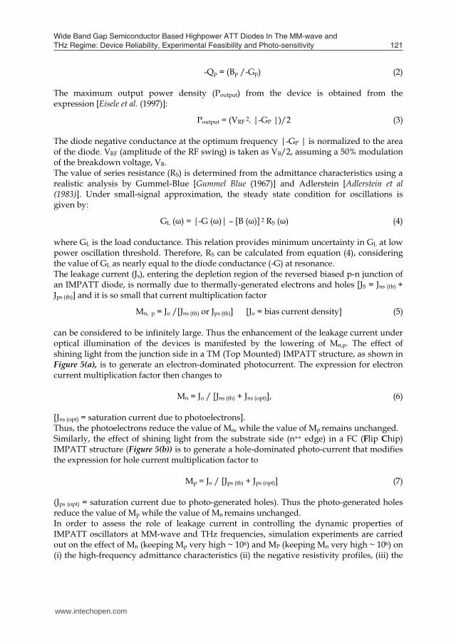
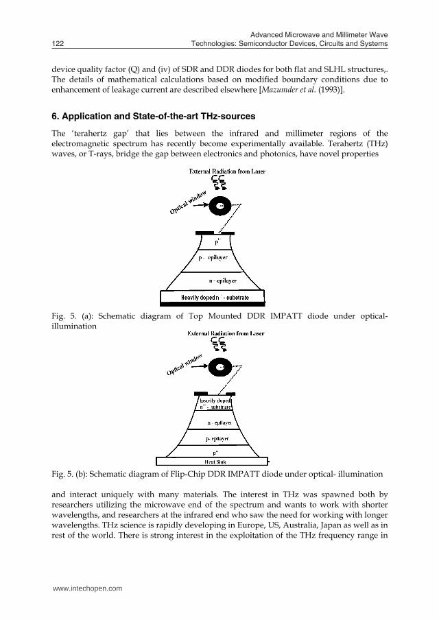
Mn, p = Jo /[Jns (th) or Jps (th)] [Jo = bias current density] (5) can be considered to be infinitely large. Thus the enhancement of the leakage current under optical illumination of the devices is manifested by the lowering of Mn,p. The effect of shining light from the junction side in a TM (Top Mounted) IMPATT structure, as shown in Figure 5(a), is to generate an electron-dominated photocurrent. The expression for electron current multiplication factor then changes to
Mn = Jo / [Jns (th) + Jns (opt)], (6) [Jns (opt) = saturation current due to photoelectrons]. Thus, the photoelectrons reduce the value of Mn, while the value of Mp remains unchanged. Similarly, the effect of shining light from the substrate side (n++ edge) in a FC (Flip Chip) IMPATT structure (Figure 5(b)) is to generate a hole-dominated photo-current that modifies the expression for hole current multiplication factor to
Mp = Jo / [Jps (th) + Jps (opt)] (7) (Jps (opt) = saturation current due to photo-generated holes). Thus the photo-generated holes reduce the value of Mp while the value of Mn remains unchanged. In order to assess the role of leakage current in controlling the dynamic properties of IMPATT oscillators at MM-wave and THz frequencies, simulation experiments are carried out on the effect of Mn (keeping Mp very high ~ 106) and MP (keeping Mn very high ~ 106) on (i) the high-frequency admittance characteristics (ii) the negative resistivity profiles, (iii) the
www.intechopen.com
Wide Band Gap Semiconductor Based Highpower ATT Diodes In The MM-wave and THz Regime: Device Reliability, Experimental Feasibility and Photo-sensitivity 121
properties of devices, as analytical methods do not provide accurate information regarding the dc and high frequency parameters of these devices. In the present thesis, a generalized, simple and more accurate dc computer simulation method that involves simultaneous computer solution of the nonlinear Poisson’s and carrier continuity equations, as proposed by Roy et al. [15], has been adopted. DC modeling of the IMPATT devices has been made realistic by considering the effects of mobile space charge, inequality of ionization rates and drift velocities of charge carriers of the base materials and also their electric field and temperature dependence. The optimum depletion layer widths for a particular design frequency (fo) are chosen from the simple transit time formula W = 0.37 vsn,sp/ fo [16]. Here vsn and vsp are the saturated drift velocities of electrons and holes respectively. DC field and carrier current profiles for various IMPATT structures can be obtained by starting the computation from the field maximum position, at the metallurgical junction. The simulation method consists of two parts: (i) DC analysis and (ii) small-signal analysis. In the dc method, Poisson and carrier continuity equations are simultaneously solved at each point in the depletion layer, subject to appropriate boundary conditions, as described elsewhere [Roy et al (1985), Mukherjee et al (2007a)]. A very small space step is considered for the accurate numerical simulation of the equations. The DC to RF conversion efficiency () [Namordi et al. (1980)] is calculated from the semi-quantitative formula,
(%) = (VD x 100) /( x VB) (1) where, VD = voltage drop across the drift region. Also, VD = VB-VA, where, VA = voltage drop across the avalanche region and VB = Breakdown voltage. The small-signal analysis of the IMPATT diode provides significant insight into the device physics and intrinsic properties of the devices. The range of frequencies exhibiting negative conductance of the diode can easily be computed by the Gummel-Blue method [Gummel Blue (1967)]. From the dc field and current profiles, the spatially dependent ionization rates that appear in the Gummel-Blue equations are evaluated and fed as input data for the high-frequency analysis. The edges of the depletion layer of the diode, which are fixed by the dc analysis, are taken as the starting and end points for the high-frequency analysis. The spatial variation of high frequency negative resistivity and reactivity in the depletion layer of the diode are obtained under small-signal conditions by solving two second order differential equations in R(x, ) and X(x, ). R(x, ω) and X(x, ω) are the real and imaginary parts of the diode impedance Z (x,), such that Z (x,) = R(x, ω) + j X(x, ω). A generalized computer algorithm for simulation of the negative resistivity and reactivity in the space charge region is used in the analysis and described elsewhere [Roy et al (1985), Mukherjee et al (2007a)]. The total integrated diode negative resistance (ZR) and reactance (Z x) at a particular frequency (ω) and current density JDC, are computed from numerical integration of the R(x) and X(x) profiles over the active space-charge layer. The high-frequency admittance characteristics, negative resistivity profiles and device quality factor (Q) of the optimized diodes are determined by this technique after satisfying the appropriate boundary conditions for R and X, as described elsewhere [Roy et al (1985), Mukherjee et al (2007a)]. The diode quality factor (QP) at the peak frequency, is defined as the ratio of the imaginary part of the admittance to the real part of the admittance (at the peak frequency), i.e.,
-Qp = (Bp /-Gp) (2) The maximum output power density (Poutput) from the device is obtained from the expression [Eisele et al. (1997)]:
Poutput = (VRF 2. |-GP |)/2 (3) The diode negative conductance at the optimum frequency |-GP | is normalized to the area of the diode. VRF (amplitude of the RF swing) is taken as VB/2, assuming a 50% modulation of the breakdown voltage, VB. The value of series resistance (RS) is determined from the admittance characteristics using a realistic analysis by Gummel-Blue [Gummel Blue (1967)] and Adlerstein [Adlerstein et al (1983)]. Under small-signal approximation, the steady state condition for oscillations is given by:
GL (ω) = |-G (ω)| – [B (ω)] 2 RS (ω) (4) where GL is the load conductance. This relation provides minimum uncertainty in GL at low power oscillation threshold. Therefore, RS can be calculated from equation (4), considering the value of GL as nearly equal to the diode conductance (-G) at resonance. The leakage current (Js), entering the depletion region of the reversed biased p-n junction of an IMPATT diode, is normally due to thermally-generated electrons and holes [JS = Jns (th) + Jps (th)] and it is so small that current multiplication factor
Mn, p = Jo /[Jns (th) or Jps (th)] [Jo = bias current density] (5) can be considered to be infinitely large. Thus the enhancement of the leakage current under optical illumination of the devices is manifested by the lowering of Mn,p. The effect of shining light from the junction side in a TM (Top Mounted) IMPATT structure, as shown in Figure 5(a), is to generate an electron-dominated photocurrent. The expression for electron current multiplication factor then changes to
Mn = Jo / [Jns (th) + Jns (opt)], (6) [Jns (opt) = saturation current due to photoelectrons]. Thus, the photoelectrons reduce the value of Mn, while the value of Mp remains unchanged. Similarly, the effect of shining light from the substrate side (n++ edge) in a FC (Flip Chip) IMPATT structure (Figure 5(b)) is to generate a hole-dominated photo-current that modifies the expression for hole current multiplication factor to
Mp = Jo / [Jps (th) + Jps (opt)] (7) (Jps (opt) = saturation current due to photo-generated holes). Thus the photo-generated holes reduce the value of Mp while the value of Mn remains unchanged. In order to assess the role of leakage current in controlling the dynamic properties of IMPATT oscillators at MM-wave and THz frequencies, simulation experiments are carried out on the effect of Mn (keeping Mp very high ~ 106) and MP (keeping Mn very high ~ 106) on (i) the high-frequency admittance characteristics (ii) the negative resistivity profiles, (iii) the
www.intechopen.com
Advanced Microwave and Millimeter Wave Technologies: Semiconductor Devices, Circuits and Systems122
device quality factor (Q) and (iv) of SDR and DDR diodes for both flat and SLHL structures,. The details of mathematical calculations based on modified boundary conditions due to enhancement of leakage current are described elsewhere [Mazumder et al. (1993)].
6. Application and State-of-the-art THz-sources
The ‘terahertz gap’ that lies between the infrared and millimeter regions of the electromagnetic spectrum has recently become experimentally available. Terahertz (THz) waves, or T-rays, bridge the gap between electronics and photonics, have novel properties
Fig. 5. (a): Schematic diagram of Top Mounted DDR IMPATT diode under optical-illumination
Fig. 5. (b): Schematic diagram of Flip-Chip DDR IMPATT diode under optical- illumination and interact uniquely with many materials. The interest in THz was spawned both by researchers utilizing the microwave end of the spectrum and wants to work with shorter wavelengths, and researchers at the infrared end who saw the need for working with longer wavelengths. THz science is rapidly developing in Europe, US, Australia, Japan as well as in rest of the world. There is strong interest in the exploitation of the THz frequency range in
virtually all fields of basic natural science (physics, chemistry, biology) as well as medicine [Trew (2005)]. Across Europe, a number of research groups at universities and in industry are working on THz science and technologies. Indeed, in the last few years the U.S. Army and the Department of Defence have focused on the advancements of THz-frequency electronic technology and on novel applications of THz-frequency sensing. Since 1999, Terahertz imaging [Wang et al. (2003)] has become a very important application, since it may make possible a single step removal process. This will enable improved detection rates of unhealthy tissue during surgery and should lead to a decrease in the number of repeat surgeries and in morbidity. Material spectroscopy and Biomedical sensing [Naftaly et al. (2005) and Watanabe et al (2004)] is perhaps the most rapidly developing of all THz applications. THz imaging of pathogens such as anthrax is also possible and that provides novel approaches for counter-terrorism. Terahertz imaging techniques are also used for planetary and cometary sensing as well in the earth-based studies which include monitoring of ozone depletion. Spectroscopy was among the first applications of THz technology, for instance, in the development of basic THz fingerprints of simple molecules, such as water, carbon monoxide and ozone. Various rotational, vibrational and translational modes of complex organic molecules, including bio-molecules are within the THz range. These modes are unique to a particular molecule, and thus it is possible to obtain a ‘Terahertz fingerprint’ allowing for the identification of those chemical substances. The application of T-rays opens the possibilities for fast DNA analysis — in both areas of disease detection and forensics. Since THz radiation is non-ionizing, it has many potential medical applications. Apart from spectroscopic characterization, T-rays can also provide X-ray-like images. In fact, Terahertz medical imaging presents a unique solution for a variety of health-related problem, such as tissue identification through its water content, dental cavity detection and liver cancer detection [Nishizawa et al. (2005)]. The most important fact is that, as the photon energy of THz is much less compared to X-ray, it is not considered intrinsically harmful to living tissues as are of X-ray. It has the ability to penetrate a few millimeters of the uppermost skin layer, and thus the early detection of skin cancer is possible. Scientists believe that the Terahertz spectrum is one of the critical technologies for defence against suicide bombers and other terrorist activities [Karpowicz et al. (2005)]. Now-a-days, researchers have focused their attention on the potential applications of Terahertz rays for directly detecting and imaging concealed weapons and explosives. Terahertz radiation can be transmitted through most non-metallic and non-polar mediums. When a Terahertz system is used properly, people can see through concealing barriers such as packaging, corrugated cardboard, walls, clothing, shoes, book bags, pill coatings, etc. Once the rays penetrate those materials, they can also characterize what might be hidden –be they explosives, chemical agents or others, based on a spectral fingerprint. Undoubtedly, security systems of the near future will incorporate THz technologies. It will be increasingly necessary to scan for biological, chemical and other weapons in a manner that is non-invasive and fast. Terahertz sensing provides advantages to short-range radar sensing, as they can penetrate through fog further than optical radiation. The wavelength being short enough, it provides significantly higher bandwidth than microwaves. However, the wavelength is long enough than infrared to reduce Rayleigh scattering and thus it find its application in short-range battlefield communication, where smoke prevails the infrared transmission. The advantage of THz over IR for indoor applications is that it occupies an
www.intechopen.com

Wide Band Gap Semiconductor Based Highpower ATT Diodes In The MM-wave and THz Regime: Device Reliability, Experimental Feasibility and Photo-sensitivity 123
device quality factor (Q) and (iv) of SDR and DDR diodes for both flat and SLHL structures,. The details of mathematical calculations based on modified boundary conditions due to enhancement of leakage current are described elsewhere [Mazumder et al. (1993)].
6. Application and State-of-the-art THz-sources
The ‘terahertz gap’ that lies between the infrared and millimeter regions of the electromagnetic spectrum has recently become experimentally available. Terahertz (THz) waves, or T-rays, bridge the gap between electronics and photonics, have novel properties
Fig. 5. (a): Schematic diagram of Top Mounted DDR IMPATT diode under optical-illumination
Fig. 5. (b): Schematic diagram of Flip-Chip DDR IMPATT diode under optical- illumination and interact uniquely with many materials. The interest in THz was spawned both by researchers utilizing the microwave end of the spectrum and wants to work with shorter wavelengths, and researchers at the infrared end who saw the need for working with longer wavelengths. THz science is rapidly developing in Europe, US, Australia, Japan as well as in rest of the world. There is strong interest in the exploitation of the THz frequency range in
virtually all fields of basic natural science (physics, chemistry, biology) as well as medicine [Trew (2005)]. Across Europe, a number of research groups at universities and in industry are working on THz science and technologies. Indeed, in the last few years the U.S. Army and the Department of Defence have focused on the advancements of THz-frequency electronic technology and on novel applications of THz-frequency sensing. Since 1999, Terahertz imaging [Wang et al. (2003)] has become a very important application, since it may make possible a single step removal process. This will enable improved detection rates of unhealthy tissue during surgery and should lead to a decrease in the number of repeat surgeries and in morbidity. Material spectroscopy and Biomedical sensing [Naftaly et al. (2005) and Watanabe et al (2004)] is perhaps the most rapidly developing of all THz applications. THz imaging of pathogens such as anthrax is also possible and that provides novel approaches for counter-terrorism. Terahertz imaging techniques are also used for planetary and cometary sensing as well in the earth-based studies which include monitoring of ozone depletion. Spectroscopy was among the first applications of THz technology, for instance, in the development of basic THz fingerprints of simple molecules, such as water, carbon monoxide and ozone. Various rotational, vibrational and translational modes of complex organic molecules, including bio-molecules are within the THz range. These modes are unique to a particular molecule, and thus it is possible to obtain a ‘Terahertz fingerprint’ allowing for the identification of those chemical substances. The application of T-rays opens the possibilities for fast DNA analysis — in both areas of disease detection and forensics. Since THz radiation is non-ionizing, it has many potential medical applications. Apart from spectroscopic characterization, T-rays can also provide X-ray-like images. In fact, Terahertz medical imaging presents a unique solution for a variety of health-related problem, such as tissue identification through its water content, dental cavity detection and liver cancer detection [Nishizawa et al. (2005)]. The most important fact is that, as the photon energy of THz is much less compared to X-ray, it is not considered intrinsically harmful to living tissues as are of X-ray. It has the ability to penetrate a few millimeters of the uppermost skin layer, and thus the early detection of skin cancer is possible. Scientists believe that the Terahertz spectrum is one of the critical technologies for defence against suicide bombers and other terrorist activities [Karpowicz et al. (2005)]. Now-a-days, researchers have focused their attention on the potential applications of Terahertz rays for directly detecting and imaging concealed weapons and explosives. Terahertz radiation can be transmitted through most non-metallic and non-polar mediums. When a Terahertz system is used properly, people can see through concealing barriers such as packaging, corrugated cardboard, walls, clothing, shoes, book bags, pill coatings, etc. Once the rays penetrate those materials, they can also characterize what might be hidden –be they explosives, chemical agents or others, based on a spectral fingerprint. Undoubtedly, security systems of the near future will incorporate THz technologies. It will be increasingly necessary to scan for biological, chemical and other weapons in a manner that is non-invasive and fast. Terahertz sensing provides advantages to short-range radar sensing, as they can penetrate through fog further than optical radiation. The wavelength being short enough, it provides significantly higher bandwidth than microwaves. However, the wavelength is long enough than infrared to reduce Rayleigh scattering and thus it find its application in short-range battlefield communication, where smoke prevails the infrared transmission. The advantage of THz over IR for indoor applications is that it occupies an
www.intechopen.com
Advanced Microwave and Millimeter Wave Technologies: Semiconductor Devices, Circuits and Systems124
extremely quiet band without noise or background clutter. Conventional wireless techniques for communication use microwaves at very low power. THz could increase the rate of information transfer as well as the volume. Now-a-days wireless communication technology requires more bandwidth for communication and data transfer. Although the high atmospheric attenuation at terahertz frequencies makes it difficult to have a long range mobile-communication, however a high-bandwidth, short-range and line of sight wireless link is completely realizable [Nagatsuma et al. (2004)]. On the other hand, atmospheric attenuation has an advantage in the reduction of coverage range of the signal in military applications to avoid communication being overheard or in frequency re-use application to avoid signal interfering. Although all other areas of the electromagnetic spectrum are used in current technologies, development of technologies in the THz region is very difficult. The reason for this lies in the lack of suitable THz sources and receivers. Thus a critical roadblock to full exploitation of the THz band is lack of reliable, powerful (0.1W – 10.0 W CW), efficient, compact and relatively inexpensive THz radiation sources. Some of the existing THz sources are: electron beam sources, optically pumped far-infrared gas lasers, frequency multipliers, photoconductive emitters, terahertz semiconductor lasers, terahertz photo-mixers, solid-state sources, etc. Among electron beam sources, Gyrotrons [Flech et al. (1999)], free electron lasers [Krishnagopal et al. (2004)], backward wave oscillators (BWO) [Dobroiu et al. (2004)] are capable of generating high-power at THz frequency region. Gyrotrons with 1 MW power at 140 GHz [Dammertz et al. (2002)] is feasible. Free electron lasers (FEL) are capable of operating virtually over the entire electromagnetic spectrum. A free electron laser at the University of California works at far infrared region and can generate 1 KW quasi-continuous wave signal at 300 GHz. BWOs can generate 50.0 mW of power at 300 GHz down to a few mW at 1 THz [Schmidt et al. (2002)]. The commercially available systems provided by Russian Company ISTOK can generate 1- 10 mW output power within the frequency range 177 GHz – 1.1 THz. Complete systems are heavy and large and need high bias voltage and water cooling systems [Ives et al. (2003)] , but the systems are much smaller than FEL and Gyrotrons. Electron beam devices are bulky and needs extremely high fields as well as high current densities which are main disadvantages of these devices. Optically pumped far infrared gas lasers can produce terahertz signals. These THz sources consists of CO2 pump laser injected into a cavity filled with a gas that help to produce THz signal [Chao et al. (2009)]. Semiconductor lasers show great promise for narrowband THz generation. Such lasers have many inherent limitations including low efficiency, low output power and the need for cryogenic cooling to maintain lasing conditions. The Quantum Cascade Laser (QCL) is the most promising THz semiconductor laser. Barbieri et al. has fabricated a continuous wave QCL that can generate 25 µW power at 4.4 THz at 52 K [Barbieri et al.(2003)]. Recently, the highest power THz source, pumped by an eye-safe, narrow band fiber laser system with an output of 26.4 mW, has been developed [Leigh et al. (2009)]. Among all two terminal solid-state sources, higher RF power levels of 23 µW at the fundamental frequency of 342 GHz and 0.6 µW at the third harmonic frequency of 1.02 THz is measured with Resonant Tunneling Diode (RTD) in the GaInAs/AlAs material systems, but these devices were operated in a “quasi CW mode” with a pulse length of 0.3 ms and a repetition rate of 300 Hz [Orihashi et al. (2005)]. State-of-the-art Gunn devices generate 0.2 – 5
µW power at 400 – 560 GHz frequencies [Eisele et al. (2005)]. Presently the maximum operating frequency range of TUNNETT devices is 355 GHz with power output of 140 µW [Eisele (2005)]. IMPact Avalanche Transit Time (IMPATT) diodes are recognized as the most powerful two terminal sources. Higher RF power and oscillation frequency were achieved from these devices by cooling he heat-sink of the diode and the waveguide circuit to 77K (liquid nitrogen) [2.11]. State-of-the-art IMPATT devices generate 2 mW- 7.5 mW power in the 300-400 GHz frequency range [Ishibashi et al. (1977)]. The above review shows that compact, low-cost but high-power and efficient THz sources are still lacking. Researchers have focused their attention in developing such THz sources to overcome the present limitation of THz systems. Research is continuing to increase the frequency and power level of conventional Si and GaAs based IMPATT devices to reach the THz region and also using alternate semiconductor material, such as, SiC and GaN together with improved fabrication techniques.
7. WBG semiconductors for fabricating high-power IMPATTs
The material parameters of the base semiconductors play an important role in deciding the operating frequency and output power level of IMPATT devices. So, the base semiconductor material should be chosen selectively to design high-power, high-frequency devices. The classification of WBG semiconductors is varied. Since the primary physical properties of a semiconductor scale to a certain degree with the energy gap, this parameter provides a reasonable classification scheme. However, comparison with Si and GaAs are common, because of the importance of these common materials. So, in general a WBG semiconductor is classified as a material with a bandgap at least twice the bandgap of Si. This gives a range from about 2eV (with InN and 3C-SiC) up to 6 eV (with AlN and diamond). WBG semiconductors, especially the Silicon Carbide (SiC) family and III-Nitride (GaN and its compounds) family are relatively attractive for developing new generation devices. Although the properties of these materials are very favorable, they are not as technologically mature as Si and GaAs. Rapid progress has been made in resolving the technological problems of the wide band gap semiconductors related to crystal growth, contact formation, material purity and quality. SiC is recognized as a semiconductor of great importance in electronic applications because of its distinct properties, the possibility of easy growth on a native oxide, and the presence of numerous polytypes [Elasser et al. (2002)]. The SiC family of semiconductor contains the same semiconductor material grown in many polytypes. The most commonly grown SiC materials are 4H-SiC, 6H-SiC, 3C-SiC. SiC, although of varied polytypes, generally have high carrier saturation velocity and high thermal conductivity, which make them suitable for high-temperature (above 800K), high-frequency (Terahertz region) applications. Cree Research Inc. was the first commercial vendor of SiC wafers which are commercially available as 4–inch wafers of 4H-SiC. It is well known that SiC wafer quality deficiencies are delaying the realization of outstandingly superior 4H-SiC high-power semiconductor devices. While efforts to date have centered on eradicating micropipes, 4H-SiC wafers and epilayers also contain elementary screw dislocations in densities of the order of thousands per cm2, nearly 100 fold micropipe densities [Dudley et al. (1995)]. While not nearly as detrimental to SiC device performances as micropipes, it was shown earlier that diodes containing elementary screw dislocations exhibit a 5% to 35% reduction in breakdown
www.intechopen.com

Wide Band Gap Semiconductor Based Highpower ATT Diodes In The MM-wave and THz Regime: Device Reliability, Experimental Feasibility and Photo-sensitivity 125
extremely quiet band without noise or background clutter. Conventional wireless techniques for communication use microwaves at very low power. THz could increase the rate of information transfer as well as the volume. Now-a-days wireless communication technology requires more bandwidth for communication and data transfer. Although the high atmospheric attenuation at terahertz frequencies makes it difficult to have a long range mobile-communication, however a high-bandwidth, short-range and line of sight wireless link is completely realizable [Nagatsuma et al. (2004)]. On the other hand, atmospheric attenuation has an advantage in the reduction of coverage range of the signal in military applications to avoid communication being overheard or in frequency re-use application to avoid signal interfering. Although all other areas of the electromagnetic spectrum are used in current technologies, development of technologies in the THz region is very difficult. The reason for this lies in the lack of suitable THz sources and receivers. Thus a critical roadblock to full exploitation of the THz band is lack of reliable, powerful (0.1W – 10.0 W CW), efficient, compact and relatively inexpensive THz radiation sources. Some of the existing THz sources are: electron beam sources, optically pumped far-infrared gas lasers, frequency multipliers, photoconductive emitters, terahertz semiconductor lasers, terahertz photo-mixers, solid-state sources, etc. Among electron beam sources, Gyrotrons [Flech et al. (1999)], free electron lasers [Krishnagopal et al. (2004)], backward wave oscillators (BWO) [Dobroiu et al. (2004)] are capable of generating high-power at THz frequency region. Gyrotrons with 1 MW power at 140 GHz [Dammertz et al. (2002)] is feasible. Free electron lasers (FEL) are capable of operating virtually over the entire electromagnetic spectrum. A free electron laser at the University of California works at far infrared region and can generate 1 KW quasi-continuous wave signal at 300 GHz. BWOs can generate 50.0 mW of power at 300 GHz down to a few mW at 1 THz [Schmidt et al. (2002)]. The commercially available systems provided by Russian Company ISTOK can generate 1- 10 mW output power within the frequency range 177 GHz – 1.1 THz. Complete systems are heavy and large and need high bias voltage and water cooling systems [Ives et al. (2003)] , but the systems are much smaller than FEL and Gyrotrons. Electron beam devices are bulky and needs extremely high fields as well as high current densities which are main disadvantages of these devices. Optically pumped far infrared gas lasers can produce terahertz signals. These THz sources consists of CO2 pump laser injected into a cavity filled with a gas that help to produce THz signal [Chao et al. (2009)]. Semiconductor lasers show great promise for narrowband THz generation. Such lasers have many inherent limitations including low efficiency, low output power and the need for cryogenic cooling to maintain lasing conditions. The Quantum Cascade Laser (QCL) is the most promising THz semiconductor laser. Barbieri et al. has fabricated a continuous wave QCL that can generate 25 µW power at 4.4 THz at 52 K [Barbieri et al.(2003)]. Recently, the highest power THz source, pumped by an eye-safe, narrow band fiber laser system with an output of 26.4 mW, has been developed [Leigh et al. (2009)]. Among all two terminal solid-state sources, higher RF power levels of 23 µW at the fundamental frequency of 342 GHz and 0.6 µW at the third harmonic frequency of 1.02 THz is measured with Resonant Tunneling Diode (RTD) in the GaInAs/AlAs material systems, but these devices were operated in a “quasi CW mode” with a pulse length of 0.3 ms and a repetition rate of 300 Hz [Orihashi et al. (2005)]. State-of-the-art Gunn devices generate 0.2 – 5
µW power at 400 – 560 GHz frequencies [Eisele et al. (2005)]. Presently the maximum operating frequency range of TUNNETT devices is 355 GHz with power output of 140 µW [Eisele (2005)]. IMPact Avalanche Transit Time (IMPATT) diodes are recognized as the most powerful two terminal sources. Higher RF power and oscillation frequency were achieved from these devices by cooling he heat-sink of the diode and the waveguide circuit to 77K (liquid nitrogen) [2.11]. State-of-the-art IMPATT devices generate 2 mW- 7.5 mW power in the 300-400 GHz frequency range [Ishibashi et al. (1977)]. The above review shows that compact, low-cost but high-power and efficient THz sources are still lacking. Researchers have focused their attention in developing such THz sources to overcome the present limitation of THz systems. Research is continuing to increase the frequency and power level of conventional Si and GaAs based IMPATT devices to reach the THz region and also using alternate semiconductor material, such as, SiC and GaN together with improved fabrication techniques.
7. WBG semiconductors for fabricating high-power IMPATTs
The material parameters of the base semiconductors play an important role in deciding the operating frequency and output power level of IMPATT devices. So, the base semiconductor material should be chosen selectively to design high-power, high-frequency devices. The classification of WBG semiconductors is varied. Since the primary physical properties of a semiconductor scale to a certain degree with the energy gap, this parameter provides a reasonable classification scheme. However, comparison with Si and GaAs are common, because of the importance of these common materials. So, in general a WBG semiconductor is classified as a material with a bandgap at least twice the bandgap of Si. This gives a range from about 2eV (with InN and 3C-SiC) up to 6 eV (with AlN and diamond). WBG semiconductors, especially the Silicon Carbide (SiC) family and III-Nitride (GaN and its compounds) family are relatively attractive for developing new generation devices. Although the properties of these materials are very favorable, they are not as technologically mature as Si and GaAs. Rapid progress has been made in resolving the technological problems of the wide band gap semiconductors related to crystal growth, contact formation, material purity and quality. SiC is recognized as a semiconductor of great importance in electronic applications because of its distinct properties, the possibility of easy growth on a native oxide, and the presence of numerous polytypes [Elasser et al. (2002)]. The SiC family of semiconductor contains the same semiconductor material grown in many polytypes. The most commonly grown SiC materials are 4H-SiC, 6H-SiC, 3C-SiC. SiC, although of varied polytypes, generally have high carrier saturation velocity and high thermal conductivity, which make them suitable for high-temperature (above 800K), high-frequency (Terahertz region) applications. Cree Research Inc. was the first commercial vendor of SiC wafers which are commercially available as 4–inch wafers of 4H-SiC. It is well known that SiC wafer quality deficiencies are delaying the realization of outstandingly superior 4H-SiC high-power semiconductor devices. While efforts to date have centered on eradicating micropipes, 4H-SiC wafers and epilayers also contain elementary screw dislocations in densities of the order of thousands per cm2, nearly 100 fold micropipe densities [Dudley et al. (1995)]. While not nearly as detrimental to SiC device performances as micropipes, it was shown earlier that diodes containing elementary screw dislocations exhibit a 5% to 35% reduction in breakdown
www.intechopen.com
Advanced Microwave and Millimeter Wave Technologies: Semiconductor Devices, Circuits and Systems126
voltage, higher pre-breakdown reverse leakage current, softer reverse breakdown I-V knee and concentrated microplasmic breakdown current filaments when measured under DC testing conditions. The cubic phase, 3C-SiC, however, is difficult to grow because of lack of a suitable substrate, thus it receives less interest. However, in recent years, there has been some little interest in 3C-SiC, resulting in both experimental and theoretical works. The most difficult to grow is 2H-SiC, because of its high formation energy. The most common donors in SiC are nitrogen (N) and phosphorous (P). N substitutes on C sites in the lattice, while P on Si sites. The most common acceptors are aluminum (Al) and boron (B) which substitutes on Si sites. SiC was considered to be a promising material for fabrication of IMPATT diodes for the first time in 1973 by Keys [Keys (1973)]. Historically, the first simulation work on modeling and analysis of SiC IMPATT devices was done by Mehdi [Mehdi et al. (1988)]. They adopted the drift-diffusion method for analyzing the microwave and MM-wave characteristics of these diodes. The device operating characteristics and the power generating capabilities of the devices were studied at four different operating frequencies, 10 GHz, 35 GHz, 60 GHz and 94 GHz. Many material parameters, such as, field and temperature dependent saturation velocities and ionization coefficients of charge carriers in SiC were not available at that time and hence these were not considered in the simulation scheme. Their study however predicted that performances of SiC devices are superior to Si devices under CW mode of operation. In 1998, Meng et al. [Meng et al. (1998)] carried out a Read-type simulation analysis of p+n Single Drift flat profile MM-Wave IMPATT devices at 800K. The simulation demonstrates that the efficiency (DC power density) for the device is 12.4% (6.7MW cm-2), 15% (4.5 MW cm-2) and 15.8% (3.3MW cm-2) for frequencies of 200, 100 and 50 GHz, respectively. A Read diode analysis is less accurate at the efficiency fall-off frequencies because there is no well defined avalanche region at the frequencies where efficiencies falls off. However, the study confirms the efficiency and power advantages of MM-Wave SiC IMPATT oscillators. Later, Zhao [Zhao et al. (2000)] have reported the Monte Carlo Particle simulation of 4H-SiC based hi-lo SDR IMPATT diode at 200 GHz. A low voltage (Vdc = 74 V) 4H-SiC IMPATT diode was designed by them to offer an efficiency of 10% at around 200 GHz with a peak output power of 11 W. These promising theoretical results attracted the attention of experimentalists. Several research groups started the realization of 4H-SiC based IMPATT. In 1998, Konstantinov et al. fabricated epitaxial p-n diodes in 4H-SiC with uniform avalanche multiplications and breakdown [Konstantinov et al. (1998)]. They have performed photo-multiplication measurement to determine electron and hole ionization rates. P-n junction diodes were fabricated from p+ -n0 -n+ epitaxial structures grown by vapor phase epitaxy (VPE); n0 and n+ layers were deposited on the p+ substrates. The substrates were oriented in (0001) crystal plane with a small off-orientation angle, 3.50 or lower. The photo-multiplication measurement revealed that impact ionization in 4H-SiC appears to be dominated by holes, a hole to electron ionization co-efficient ratio up to 40-50 was observed. This ionization rate asymmetry was related to band-structure effects, to the discontinuity of the conduction band or the electron momentum along the c-direction. The results had a qualitative agreement with earlier studies of impact ionization in 6H-SiC. In 6H-SiC also, electron impact ionization was strongly suppressed and that was contributed to the discontinuity of the electron energy spectrum in the conduction band. Earlier problems in SiC device development due to poor material quality and immature device processing techniques was
greatly overcome with the availability of production-quality substrates and the progress made in the processing technology. Though excellent microwave performances were demonstrated in SiC MESFETs and Static Induction transistors (SIT) [Brandt (1998)], no experimental work was reported for SiC IMPATT devices before 2000. First experimental success of 4H-SiC based pulsed mode IMPATT was achieved by Yuan et al. (2001). The DC characteristics of the high-low diodes exhibited hard, sustainable avalanche breakdown, as required for IMPATT operation. The fabricated 75 µm diameter SiC diodes were found to oscillate at 7.75 GHz at a power level of 1 mW. However, the output power level was significantly lower than the expected simulated value. They pointed out that the low-power problem is related to the measurement systems, particularly the design of the bias line. Optimization of the microwave circuit, in which the diode is embedded, is very important to properly evaluate the device performance. Any dispute in circuit optimization causes severe reduction in output power level. Thus, Yuan et al. made a comment that the measured low power, as obtained by their group, does not reflect the true power capability of SiC IMPATT. Vassilevski et al. (2001) also fabricated 4H-SiC based IMPATT. Microwave pulsed power of 300 mW was measured at 10 GHz. Though a comparatively higher power level was achieved, the power conversion efficiency was found to be very low ~0.3%. To increase the output power level, Ono et al. (2005) introduced a highly resistive guard ring that surrounds the diode periphery. The advantage of this guard ring is to reduce the electric field at the p-n junction edge of the junction periphery. A high current can thus be supplied through the diode without any destruction. Output power of 1.8W at 11.93 GHz was obtained from their fabricated diode and which is till date the highest reported output power from 4H-SiC IMPATT diodes. Nevertheless this power level is much lower than that expected. To increase the output power level, as expected from simulation studies, the residual series resistance should be minimized. No theoretical or experimental works on lo-hi-lo type 4H-SiC-based diodes are published by other workers. To the best of author’s knowledge, no experimental results are available for 6H-SiC based IMPATTs. Hence, it was established that at MM-wave region, 6H-SiC is another suitable candidate for developing high-power IMPATT devices. The III-Nitride family of semiconductors can fill the emerging market for semiconductor optoelectronic devices. One of the important advantages of GaN over SiC is the ability to form heterojunctions. The fact that GaN together with InN and AlN, allows the formation of heterostructures provides some interesting device possibilities. The III-Nitride family consists of the binary semiconductors; InN, AlN and GaN, and the ternaries composed of them, Alx G1-x N and Inx Al1-x N. GaN can be grown in two phases: zinc-blende (cubic) and wurtzite (hexagonal), while the remaining III-Nitride semiconductors only have the wurtzite polytype. The III-Nitride family of materials has gain interest in both opto-electronic and high-power solid-state devices. Their technological immaturity is mainly due to fabrication problems; however in recent years, advances have been made in the wurtzite-phase versions. Again as with the SiC family, wurtzite-phase materials receive most of the attention because of the relative ease of growth when compared to zinc-blende GaN. Commercial GaN based devices are grown heteroepitaxially on substrates like Sapphire and SiC. Recently, Si has been considered as a substrate for GaN growth for its low price, high crystalline quality and potential capabilities for integration with traditional Si-based electronic technology. MOCVD has become the technique of choice
www.intechopen.com
Wide Band Gap Semiconductor Based Highpower ATT Diodes In The MM-wave and THz Regime: Device Reliability, Experimental Feasibility and Photo-sensitivity 127
voltage, higher pre-breakdown reverse leakage current, softer reverse breakdown I-V knee and concentrated microplasmic breakdown current filaments when measured under DC testing conditions. The cubic phase, 3C-SiC, however, is difficult to grow because of lack of a suitable substrate, thus it receives less interest. However, in recent years, there has been some little interest in 3C-SiC, resulting in both experimental and theoretical works. The most difficult to grow is 2H-SiC, because of its high formation energy. The most common donors in SiC are nitrogen (N) and phosphorous (P). N substitutes on C sites in the lattice, while P on Si sites. The most common acceptors are aluminum (Al) and boron (B) which substitutes on Si sites. SiC was considered to be a promising material for fabrication of IMPATT diodes for the first time in 1973 by Keys [Keys (1973)]. Historically, the first simulation work on modeling and analysis of SiC IMPATT devices was done by Mehdi [Mehdi et al. (1988)]. They adopted the drift-diffusion method for analyzing the microwave and MM-wave characteristics of these diodes. The device operating characteristics and the power generating capabilities of the devices were studied at four different operating frequencies, 10 GHz, 35 GHz, 60 GHz and 94 GHz. Many material parameters, such as, field and temperature dependent saturation velocities and ionization coefficients of charge carriers in SiC were not available at that time and hence these were not considered in the simulation scheme. Their study however predicted that performances of SiC devices are superior to Si devices under CW mode of operation. In 1998, Meng et al. [Meng et al. (1998)] carried out a Read-type simulation analysis of p+n Single Drift flat profile MM-Wave IMPATT devices at 800K. The simulation demonstrates that the efficiency (DC power density) for the device is 12.4% (6.7MW cm-2), 15% (4.5 MW cm-2) and 15.8% (3.3MW cm-2) for frequencies of 200, 100 and 50 GHz, respectively. A Read diode analysis is less accurate at the efficiency fall-off frequencies because there is no well defined avalanche region at the frequencies where efficiencies falls off. However, the study confirms the efficiency and power advantages of MM-Wave SiC IMPATT oscillators. Later, Zhao [Zhao et al. (2000)] have reported the Monte Carlo Particle simulation of 4H-SiC based hi-lo SDR IMPATT diode at 200 GHz. A low voltage (Vdc = 74 V) 4H-SiC IMPATT diode was designed by them to offer an efficiency of 10% at around 200 GHz with a peak output power of 11 W. These promising theoretical results attracted the attention of experimentalists. Several research groups started the realization of 4H-SiC based IMPATT. In 1998, Konstantinov et al. fabricated epitaxial p-n diodes in 4H-SiC with uniform avalanche multiplications and breakdown [Konstantinov et al. (1998)]. They have performed photo-multiplication measurement to determine electron and hole ionization rates. P-n junction diodes were fabricated from p+ -n0 -n+ epitaxial structures grown by vapor phase epitaxy (VPE); n0 and n+ layers were deposited on the p+ substrates. The substrates were oriented in (0001) crystal plane with a small off-orientation angle, 3.50 or lower. The photo-multiplication measurement revealed that impact ionization in 4H-SiC appears to be dominated by holes, a hole to electron ionization co-efficient ratio up to 40-50 was observed. This ionization rate asymmetry was related to band-structure effects, to the discontinuity of the conduction band or the electron momentum along the c-direction. The results had a qualitative agreement with earlier studies of impact ionization in 6H-SiC. In 6H-SiC also, electron impact ionization was strongly suppressed and that was contributed to the discontinuity of the electron energy spectrum in the conduction band. Earlier problems in SiC device development due to poor material quality and immature device processing techniques was
greatly overcome with the availability of production-quality substrates and the progress made in the processing technology. Though excellent microwave performances were demonstrated in SiC MESFETs and Static Induction transistors (SIT) [Brandt (1998)], no experimental work was reported for SiC IMPATT devices before 2000. First experimental success of 4H-SiC based pulsed mode IMPATT was achieved by Yuan et al. (2001). The DC characteristics of the high-low diodes exhibited hard, sustainable avalanche breakdown, as required for IMPATT operation. The fabricated 75 µm diameter SiC diodes were found to oscillate at 7.75 GHz at a power level of 1 mW. However, the output power level was significantly lower than the expected simulated value. They pointed out that the low-power problem is related to the measurement systems, particularly the design of the bias line. Optimization of the microwave circuit, in which the diode is embedded, is very important to properly evaluate the device performance. Any dispute in circuit optimization causes severe reduction in output power level. Thus, Yuan et al. made a comment that the measured low power, as obtained by their group, does not reflect the true power capability of SiC IMPATT. Vassilevski et al. (2001) also fabricated 4H-SiC based IMPATT. Microwave pulsed power of 300 mW was measured at 10 GHz. Though a comparatively higher power level was achieved, the power conversion efficiency was found to be very low ~0.3%. To increase the output power level, Ono et al. (2005) introduced a highly resistive guard ring that surrounds the diode periphery. The advantage of this guard ring is to reduce the electric field at the p-n junction edge of the junction periphery. A high current can thus be supplied through the diode without any destruction. Output power of 1.8W at 11.93 GHz was obtained from their fabricated diode and which is till date the highest reported output power from 4H-SiC IMPATT diodes. Nevertheless this power level is much lower than that expected. To increase the output power level, as expected from simulation studies, the residual series resistance should be minimized. No theoretical or experimental works on lo-hi-lo type 4H-SiC-based diodes are published by other workers. To the best of author’s knowledge, no experimental results are available for 6H-SiC based IMPATTs. Hence, it was established that at MM-wave region, 6H-SiC is another suitable candidate for developing high-power IMPATT devices. The III-Nitride family of semiconductors can fill the emerging market for semiconductor optoelectronic devices. One of the important advantages of GaN over SiC is the ability to form heterojunctions. The fact that GaN together with InN and AlN, allows the formation of heterostructures provides some interesting device possibilities. The III-Nitride family consists of the binary semiconductors; InN, AlN and GaN, and the ternaries composed of them, Alx G1-x N and Inx Al1-x N. GaN can be grown in two phases: zinc-blende (cubic) and wurtzite (hexagonal), while the remaining III-Nitride semiconductors only have the wurtzite polytype. The III-Nitride family of materials has gain interest in both opto-electronic and high-power solid-state devices. Their technological immaturity is mainly due to fabrication problems; however in recent years, advances have been made in the wurtzite-phase versions. Again as with the SiC family, wurtzite-phase materials receive most of the attention because of the relative ease of growth when compared to zinc-blende GaN. Commercial GaN based devices are grown heteroepitaxially on substrates like Sapphire and SiC. Recently, Si has been considered as a substrate for GaN growth for its low price, high crystalline quality and potential capabilities for integration with traditional Si-based electronic technology. MOCVD has become the technique of choice
www.intechopen.com

Advanced Microwave and Millimeter Wave Technologies: Semiconductor Devices, Circuits and Systems128
for the epitaxial growth of GaN material and devices [Pearton (2000)]. In MOCVD growth, Si and Mg are used as donor and acceptor impurities, respectively. Very recently, halide-hydride vapor phase epitaxy (HVPE) is considered as a promising technique for the fabrication of GaN based device structures, particularly for the GaN/SiC heterostructure. Reliable low-resistance ohmic contacts are essential for efficient device operation. Ohmic contact processing is still a challenging area in device technology. P- and n- type ohmic contact resistances of SiC and GaN will be discussed in the relevant chapters of the thesis. Despite decades of study, only recently GaN-based materials have moved from research laboratories to commercial markets. This change was due to a rapid progression of improvements in epitaxial growth, demonstration of p-type conductivity and the fabrication of commercially viable devices. The fabrication of highly efficient blue and green LEDs and diode lasers is driving the development of GaN-technology. The robust and versatile properties of GaN make it an excellent candidate for high-speed and high-power electronics. Interest in GaN has exploded in past few years, leading to an expansion of its potential applications on an almost monthly basis [Kuzuhara et al. (2009)]. This broad spectrum of applications has led some to predict that GaN will eventually become the third most important semiconductor material, behind Si and GaAs. High-power handeling of GaN power transistors have already been demonstrated by fabrication of GaN High Electron Mobility Transistors (HEMT) and Field Effect Transistor (FET) devices [Pearton (2000)]. No experimental work, however, has been reported for GaN IMPATT diodes, despite the fact that the diodes are easier to fabricate than transistors. Till date, only a few simulation results on GaN based IMPATT have been reported in published journals. Meng et al. (1999) studied the MM-Wave performances of the wurtzite phase and zinc-blende phase GaN IMPATT devices at 800K by a Read-type modeling approach. The simulations showed that GaN wurtzite-phase p-n single drift flat-profile IMPATT oscillators at 300 GHz have an efficiency of 11% and an RF power density of 1.6 MW.cm-2. Their studies confirm the efficiency and power density advantages of GaN IMPATT oscillators. A. K. Panda et al. (2001) designed and studied the performances of GaN based IMPATTs in the D-band. The maximum power that may be obtained from their designed diode was 3.775 W with an efficiency of 12.5%. Moreover, their study predicted that the wurtzite-phase GaN based IMPATT is better than its zinc- blend counterpart, as far as breakdown voltage, power output and efficiency are concerned. Later, Reklaitis et al. (2005) performed a Monte Carlo simulation of Wz-GaN based near-terahertz IMPATT diode. Their analysis predicted that the device may generate a RF power of ~ 3W at 0.45 THz with an efficiency of 18%. The diodes were found to be more efficient than that was designed by Panda et al. This study, on the other hand, predicted the possibilities of GaN based IMPATT diodes as efficient near-THz power sources. Alekseev et al. (2000) performed theoretical and experimental studies for the development and optimization of GaN based Gunn devices in the THz frequency region. GaN Gunn-diode oscillators at 750 GHz are expected to generate power density of 3x10⁵W cm-2. Before an attempt is made to fabricate GaN based IMPATT devices at Terahertz region, reliable modeling and better understanding of high-frequency properties of such devices are essential. Thus the author has studied the DC and Terahertz -frequency characteristics of the GaN based flat and lo-hi-lo types IMPATT
devices at elevated junction temperature and the results will be discussed in the concerned chapters. Unlike GaAs, wurtzite phase GaN have different ionization rates for electrons and holes (αn ≠ αP). So from the ionization point of view, as discussed in sub-section 2.5.3, wurtzite GaN IMPATT is expected to be noisier than GaAs IMPATT. Panda et al. [2.188] showed that GaN based devices generate equal noise as Si-based IMPATTs, but higher by 6-8 dB noise values compared with GaAs based devices under the same operating conditions. However, for increased operation temperature, the noise is found to decrease [A. K. Panda et al. (2001)]. Reklaitis et al. [Reklaitis et al.(2005)] later studied the current voltage characteristics and the associated current noise in GaN double drift IMPATT diodes, by Monte Carlo simulations. For values of current multiplication factor greater than ten they observed a giant suppression of avalanche noise down to three orders of magnitude with respect to the standard excess noise factor. The negative feedback between fluctuations in space-charge and in number of generated e-h pairs is found to be responsible of such a giant suppression.
8. Superiority of WBG semiconductor based IMPATTs over Conventional diodes
4H-SiC based SDR (p++ n n++) IMPATT diodes with flat and SLHL doping profiles are designed by Mukherjee et al. (2008 a) at around Ka-band. In order to make a comparison, Si based SDR IMPATT diode is also designed at Ka-band. The comparison reveals that 4H-SiC based SDR diodes are capable of generating a RF power of 870.0 x 10⁹ Wm-2 with an efficiency of 20.0 %, far better than their Si counterpart [Mukherjee et al. (2008)]. Thereafter, the DDR IMPATT diodes are designed and studied thoroughly by Mukherjee et al. (2009 a) at three different window frequencies: 35 GHz (Ka-band), 140 GHz (D-band) and 220 GHz (Y-band) and the corresponding admittance plots are shown in Figures 6 (a-c). Comparative studies of SLHL and flat-profile diodes at MM-wave window frequencies by Mukherjee et al. (2009) reveal that the Quasi Read SLHL diodes are superior to their flat profile counterparts in terms of power output, efficiency and negative-resistance.
Fig. 6. (a) admittance plots of 4H-SiC DDR IMPATT at Ka--band
www.intechopen.com

Wide Band Gap Semiconductor Based Highpower ATT Diodes In The MM-wave and THz Regime: Device Reliability, Experimental Feasibility and Photo-sensitivity 129
for the epitaxial growth of GaN material and devices [Pearton (2000)]. In MOCVD growth, Si and Mg are used as donor and acceptor impurities, respectively. Very recently, halide-hydride vapor phase epitaxy (HVPE) is considered as a promising technique for the fabrication of GaN based device structures, particularly for the GaN/SiC heterostructure. Reliable low-resistance ohmic contacts are essential for efficient device operation. Ohmic contact processing is still a challenging area in device technology. P- and n- type ohmic contact resistances of SiC and GaN will be discussed in the relevant chapters of the thesis. Despite decades of study, only recently GaN-based materials have moved from research laboratories to commercial markets. This change was due to a rapid progression of improvements in epitaxial growth, demonstration of p-type conductivity and the fabrication of commercially viable devices. The fabrication of highly efficient blue and green LEDs and diode lasers is driving the development of GaN-technology. The robust and versatile properties of GaN make it an excellent candidate for high-speed and high-power electronics. Interest in GaN has exploded in past few years, leading to an expansion of its potential applications on an almost monthly basis [Kuzuhara et al. (2009)]. This broad spectrum of applications has led some to predict that GaN will eventually become the third most important semiconductor material, behind Si and GaAs. High-power handeling of GaN power transistors have already been demonstrated by fabrication of GaN High Electron Mobility Transistors (HEMT) and Field Effect Transistor (FET) devices [Pearton (2000)]. No experimental work, however, has been reported for GaN IMPATT diodes, despite the fact that the diodes are easier to fabricate than transistors. Till date, only a few simulation results on GaN based IMPATT have been reported in published journals. Meng et al. (1999) studied the MM-Wave performances of the wurtzite phase and zinc-blende phase GaN IMPATT devices at 800K by a Read-type modeling approach. The simulations showed that GaN wurtzite-phase p-n single drift flat-profile IMPATT oscillators at 300 GHz have an efficiency of 11% and an RF power density of 1.6 MW.cm-2. Their studies confirm the efficiency and power density advantages of GaN IMPATT oscillators. A. K. Panda et al. (2001) designed and studied the performances of GaN based IMPATTs in the D-band. The maximum power that may be obtained from their designed diode was 3.775 W with an efficiency of 12.5%. Moreover, their study predicted that the wurtzite-phase GaN based IMPATT is better than its zinc- blend counterpart, as far as breakdown voltage, power output and efficiency are concerned. Later, Reklaitis et al. (2005) performed a Monte Carlo simulation of Wz-GaN based near-terahertz IMPATT diode. Their analysis predicted that the device may generate a RF power of ~ 3W at 0.45 THz with an efficiency of 18%. The diodes were found to be more efficient than that was designed by Panda et al. This study, on the other hand, predicted the possibilities of GaN based IMPATT diodes as efficient near-THz power sources. Alekseev et al. (2000) performed theoretical and experimental studies for the development and optimization of GaN based Gunn devices in the THz frequency region. GaN Gunn-diode oscillators at 750 GHz are expected to generate power density of 3x10⁵W cm-2. Before an attempt is made to fabricate GaN based IMPATT devices at Terahertz region, reliable modeling and better understanding of high-frequency properties of such devices are essential. Thus the author has studied the DC and Terahertz -frequency characteristics of the GaN based flat and lo-hi-lo types IMPATT
devices at elevated junction temperature and the results will be discussed in the concerned chapters. Unlike GaAs, wurtzite phase GaN have different ionization rates for electrons and holes (αn ≠ αP). So from the ionization point of view, as discussed in sub-section 2.5.3, wurtzite GaN IMPATT is expected to be noisier than GaAs IMPATT. Panda et al. [2.188] showed that GaN based devices generate equal noise as Si-based IMPATTs, but higher by 6-8 dB noise values compared with GaAs based devices under the same operating conditions. However, for increased operation temperature, the noise is found to decrease [A. K. Panda et al. (2001)]. Reklaitis et al. [Reklaitis et al.(2005)] later studied the current voltage characteristics and the associated current noise in GaN double drift IMPATT diodes, by Monte Carlo simulations. For values of current multiplication factor greater than ten they observed a giant suppression of avalanche noise down to three orders of magnitude with respect to the standard excess noise factor. The negative feedback between fluctuations in space-charge and in number of generated e-h pairs is found to be responsible of such a giant suppression.
8. Superiority of WBG semiconductor based IMPATTs over Conventional diodes
4H-SiC based SDR (p++ n n++) IMPATT diodes with flat and SLHL doping profiles are designed by Mukherjee et al. (2008 a) at around Ka-band. In order to make a comparison, Si based SDR IMPATT diode is also designed at Ka-band. The comparison reveals that 4H-SiC based SDR diodes are capable of generating a RF power of 870.0 x 10⁹ Wm-2 with an efficiency of 20.0 %, far better than their Si counterpart [Mukherjee et al. (2008)]. Thereafter, the DDR IMPATT diodes are designed and studied thoroughly by Mukherjee et al. (2009 a) at three different window frequencies: 35 GHz (Ka-band), 140 GHz (D-band) and 220 GHz (Y-band) and the corresponding admittance plots are shown in Figures 6 (a-c). Comparative studies of SLHL and flat-profile diodes at MM-wave window frequencies by Mukherjee et al. (2009) reveal that the Quasi Read SLHL diodes are superior to their flat profile counterparts in terms of power output, efficiency and negative-resistance.
Fig. 6. (a) admittance plots of 4H-SiC DDR IMPATT at Ka--band
www.intechopen.com
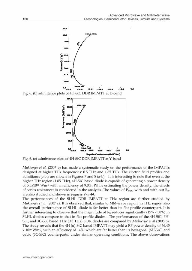
Advanced Microwave and Millimeter Wave Technologies: Semiconductor Devices, Circuits and Systems130
Fig. 6. (b) admittance plots of 4H-SiC DDR IMPATT at D-band
Fig. 6. (c) admittance plots of 4H-SiC DDR IMPATT at Y-band Mukherjee et al. (2007 b) has made a systematic study on the performance of the IMPATTs designed at higher THz frequencies: 0.5 THz and 1.85 THz. The electric field profiles and admittance plots are shown in Figures 7 and 8 (a-b). It is interesting to note that even at the higher THz region (1.85 THz), 4H-SiC based diode is capable of generating a power density of 5.0x10¹¹ Wm-2 with an efficiency of 9.0%. While estimating the power density, the effects of series resistances is considered in the analysis. The values of Pmax, with and with-out RS, are also studied and shown in Figures 9 (a-b). The performances of the SLHL DDR IMPATT at THz region are further studied by Mukherjee et al. (2007 c). It is observed that, similar to MM-wave region, in THz region also the overall performance of SLHL diode is far better than its flat profile counterpart. It is further interesting to observe that the magnitude of RS reduces significantly (15% - 30%) in SLHL diodes compare to that in flat profile diodes. The performances of the 4H-SiC, 6H-SiC, and 3C-SiC based THz (0.3 THz) DDR diodes are compared by Mukherjee et al (2008 b). The study reveals that the 4H (α)-SiC based IMPATT may yield a RF power density of 36.45 x 10¹⁰ Wm-2, with an efficiency of 14%, which are far better than its hexagonal (6H-SiC) and cubic (3C-SiC) counterparts, under similar operating conditions. The above observations
definitely establish the potential of SiC based IMPATTs at MM-wave as well in the THz region.
Fig. 7. E(x) profiles of 4H-SiC based Terabertz IMPATT diodes
Fig. 8. (a): Admittance characteristics of 4H-SiC IMPATT at 0.5 Terahertz.
www.intechopen.com

Wide Band Gap Semiconductor Based Highpower ATT Diodes In The MM-wave and THz Regime: Device Reliability, Experimental Feasibility and Photo-sensitivity 131
Fig. 6. (b) admittance plots of 4H-SiC DDR IMPATT at D-band
Fig. 6. (c) admittance plots of 4H-SiC DDR IMPATT at Y-band Mukherjee et al. (2007 b) has made a systematic study on the performance of the IMPATTs designed at higher THz frequencies: 0.5 THz and 1.85 THz. The electric field profiles and admittance plots are shown in Figures 7 and 8 (a-b). It is interesting to note that even at the higher THz region (1.85 THz), 4H-SiC based diode is capable of generating a power density of 5.0x10¹¹ Wm-2 with an efficiency of 9.0%. While estimating the power density, the effects of series resistances is considered in the analysis. The values of Pmax, with and with-out RS, are also studied and shown in Figures 9 (a-b). The performances of the SLHL DDR IMPATT at THz region are further studied by Mukherjee et al. (2007 c). It is observed that, similar to MM-wave region, in THz region also the overall performance of SLHL diode is far better than its flat profile counterpart. It is further interesting to observe that the magnitude of RS reduces significantly (15% - 30%) in SLHL diodes compare to that in flat profile diodes. The performances of the 4H-SiC, 6H-SiC, and 3C-SiC based THz (0.3 THz) DDR diodes are compared by Mukherjee et al (2008 b). The study reveals that the 4H (α)-SiC based IMPATT may yield a RF power density of 36.45 x 10¹⁰ Wm-2, with an efficiency of 14%, which are far better than its hexagonal (6H-SiC) and cubic (3C-SiC) counterparts, under similar operating conditions. The above observations
definitely establish the potential of SiC based IMPATTs at MM-wave as well in the THz region.
Fig. 7. E(x) profiles of 4H-SiC based Terabertz IMPATT diodes
Fig. 8. (a): Admittance characteristics of 4H-SiC IMPATT at 0.5 Terahertz.
www.intechopen.com
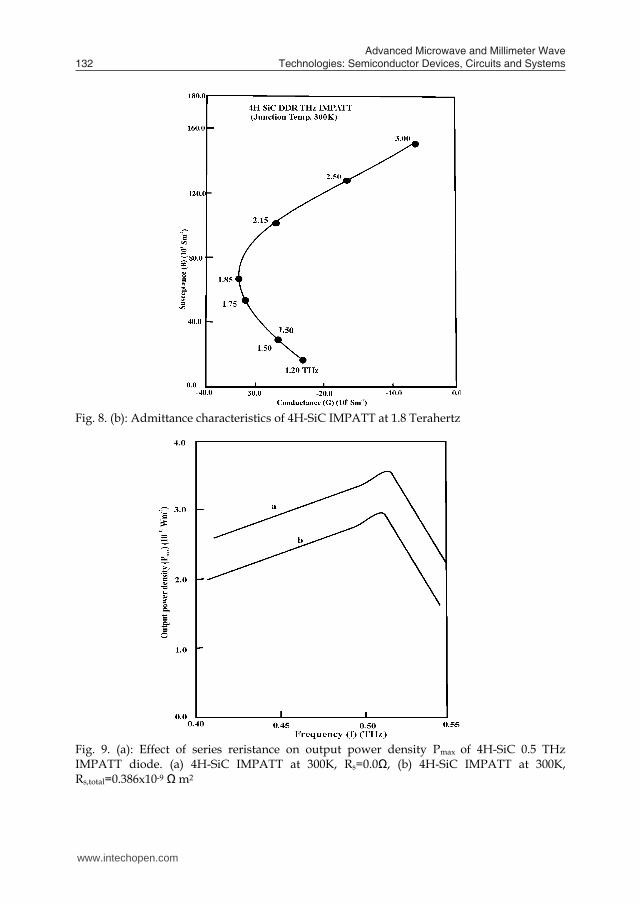
Advanced Microwave and Millimeter Wave Technologies: Semiconductor Devices, Circuits and Systems132
Fig. 8. (b): Admittance characteristics of 4H-SiC IMPATT at 1.8 Terahertz
Fig. 9. (a): Effect of series reristance on output power density Pmax of 4H-SiC 0.5 THz IMPATT diode. (a) 4H-SiC IMPATT at 300K, Rs=0.0Ω, (b) 4H-SiC IMPATT at 300K, Rs,total=0.386x10⁻⁹ Ω m2
Fig. 9. (b): Effect of series resistance on output power density (Pmax) of SiC THz IMPATT diodes. (a) 4H-SiC IMPATT at 300K, Rs=0.0Ω, (b) 4H-SiC IMPATT at 300K, Rs,total=2.2x10⁻¹¹ Ω m2
Fig. 10. Plots of electric field profile for (a) SLHL and (b) flat-type GaN (flat-profile) SDR IMPATT diodes. The distance of the n-side from the metallurgical junction has been considered as negative.
www.intechopen.com

Wide Band Gap Semiconductor Based Highpower ATT Diodes In The MM-wave and THz Regime: Device Reliability, Experimental Feasibility and Photo-sensitivity 133
Fig. 8. (b): Admittance characteristics of 4H-SiC IMPATT at 1.8 Terahertz
Fig. 9. (a): Effect of series reristance on output power density Pmax of 4H-SiC 0.5 THz IMPATT diode. (a) 4H-SiC IMPATT at 300K, Rs=0.0Ω, (b) 4H-SiC IMPATT at 300K, Rs,total=0.386x10⁻⁹ Ω m2
Fig. 9. (b): Effect of series resistance on output power density (Pmax) of SiC THz IMPATT diodes. (a) 4H-SiC IMPATT at 300K, Rs=0.0Ω, (b) 4H-SiC IMPATT at 300K, Rs,total=2.2x10⁻¹¹ Ω m2
Fig. 10. Plots of electric field profile for (a) SLHL and (b) flat-type GaN (flat-profile) SDR IMPATT diodes. The distance of the n-side from the metallurgical junction has been considered as negative.
www.intechopen.com
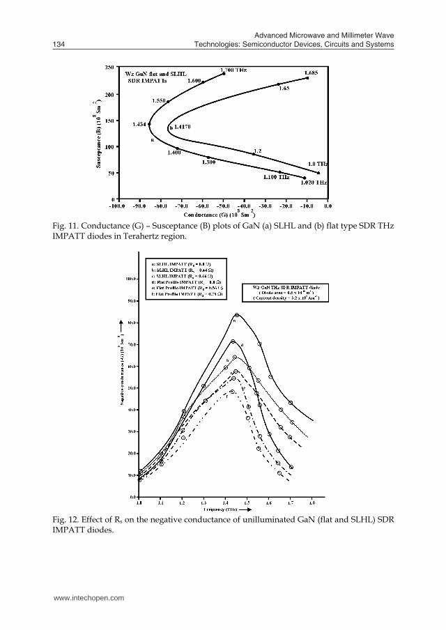
Advanced Microwave and Millimeter Wave Technologies: Semiconductor Devices, Circuits and Systems134
Fig. 11. Conductance (G) – Susceptance (B) plots of GaN (a) SLHL and (b) flat type SDR THz IMPATT diodes in Terahertz region.
Fig. 12. Effect of Rs on the negative conductance of unilluminated GaN (flat and SLHL) SDR IMPATT diodes.
Fig. 13. Effect of photo-illumination on FC and TM illumination configurations of SiC (3C, 4H and 6H types) based terahertz DDR IMPATT diodes at room temperature (300K). WZ-GaN based SDR (p++ n n++) IMPATT diode is designed and studied by Mukherjee et al. at around 140.0 GHz (D-band) frequency and the performances are compared with Si IMPATT. It is found that the GaN IMPATT may generate an output-power density of 5.6x10¹⁰ Wm-2 with an efficiency of 23.5% at 145.0 GHz, far better than Si IMPATT. The prospects of SDR flat and SLHL type GaN IMPATTs at 1.45 THz are simulated and the results are reported elsewhere [Mukherjee et al. (2007 a) ]. The studies indicate that GaN IMPATT diodes are capable of generating high power of ~2.5 W (assuming diode area = 0.5x10⁻¹⁰ m2) at around 1.45 THz with 17% -19.0 % efficiency. The effect of series resistance on the THz performance of the device is also studied by Mukherjee et al (2007 a). It is interesting to note that the presence of a charge bump in flatly doped SDR structure reduces the value of parasitic series resistance in GaN-IMPATT by ~ 22%. The electric field profiles, admittance charecteristics and effects of series resistance on Pmax of the GaN flat and SLHL diodes at 1.45 THz are shown in Figures 10, 11 and 12 [Mukherjee et al (2007 a)].
9. Photo-sensitivity of WBG semiconductor based IMPATTs
The effects of photo-illumination on the 4H-SiC, 6H-SiC and 3C-SiC based Top Mounted and Flip Chip diodes are studied by Mukherjee et al (2008 b) at THz region. It is found that the optimum frequency and THz characteristics undergo sufficient variation with increase of the intensity of optical radiation. It is interesting to note that in all the three types of SiC based IMPATTs, photo-generated leakage current dominated by holes (FC illimination configuration) is more important than that dominated by electrons (TM illumination configuration), in modulating the high frequency properties of the devices. This observation
www.intechopen.com

Wide Band Gap Semiconductor Based Highpower ATT Diodes In The MM-wave and THz Regime: Device Reliability, Experimental Feasibility and Photo-sensitivity 135
Fig. 11. Conductance (G) – Susceptance (B) plots of GaN (a) SLHL and (b) flat type SDR THz IMPATT diodes in Terahertz region.
Fig. 12. Effect of Rs on the negative conductance of unilluminated GaN (flat and SLHL) SDR IMPATT diodes.
Fig. 13. Effect of photo-illumination on FC and TM illumination configurations of SiC (3C, 4H and 6H types) based terahertz DDR IMPATT diodes at room temperature (300K). WZ-GaN based SDR (p++ n n++) IMPATT diode is designed and studied by Mukherjee et al. at around 140.0 GHz (D-band) frequency and the performances are compared with Si IMPATT. It is found that the GaN IMPATT may generate an output-power density of 5.6x10¹⁰ Wm-2 with an efficiency of 23.5% at 145.0 GHz, far better than Si IMPATT. The prospects of SDR flat and SLHL type GaN IMPATTs at 1.45 THz are simulated and the results are reported elsewhere [Mukherjee et al. (2007 a) ]. The studies indicate that GaN IMPATT diodes are capable of generating high power of ~2.5 W (assuming diode area = 0.5x10⁻¹⁰ m2) at around 1.45 THz with 17% -19.0 % efficiency. The effect of series resistance on the THz performance of the device is also studied by Mukherjee et al (2007 a). It is interesting to note that the presence of a charge bump in flatly doped SDR structure reduces the value of parasitic series resistance in GaN-IMPATT by ~ 22%. The electric field profiles, admittance charecteristics and effects of series resistance on Pmax of the GaN flat and SLHL diodes at 1.45 THz are shown in Figures 10, 11 and 12 [Mukherjee et al (2007 a)].
9. Photo-sensitivity of WBG semiconductor based IMPATTs
The effects of photo-illumination on the 4H-SiC, 6H-SiC and 3C-SiC based Top Mounted and Flip Chip diodes are studied by Mukherjee et al (2008 b) at THz region. It is found that the optimum frequency and THz characteristics undergo sufficient variation with increase of the intensity of optical radiation. It is interesting to note that in all the three types of SiC based IMPATTs, photo-generated leakage current dominated by holes (FC illimination configuration) is more important than that dominated by electrons (TM illumination configuration), in modulating the high frequency properties of the devices. This observation
www.intechopen.com

Advanced Microwave and Millimeter Wave Technologies: Semiconductor Devices, Circuits and Systems136
has been correlated with the relative ionization coefficients of charge carriers of SiC. The admittance characteristics and negative resistivity profiles of the un-illuminated and illuminated diodes are shown in Figures 13 and 14, respectively. The study reveals that the enhanced leakage current in illuminated devices, due to photo-illumination, degrades the output power density and negative resistance, but increases the tuning range of the devices. The optical illumination studies on the three types of SiC DDRs by Mukherjee et al. [Mukherjee et al (2008 b)] reveals that 4H-SiC based IMPATT is comparatively more photo-sensitive than its 6H- and 3C- counterparts. The photo-sensitivity of the 4H-SiC and 6H-SiC diodes at higher THz region (> 1 THz) are studied by Mukherjee et al. The admittance plots are shown in Figures 15 and 16. It is again found that in the higher THz region also, FC IMPATTs are more photo-sensitive than TM diodes. Compare to 4H-SiC IMPATT, 6H-SiC devices are found to be less promising in the THz region, as far as negative resistance, output power density, efficiencies and photo-sensitivity are concerned. However, it is worth mentioning that 6H-SiC based THz devices are definitely superior to conventional Si- and GaAs-based devices, since the latter categories of diodes could not reach the THz region. The effects of photo-illumination on the MM-wave and THz performances (Figures 17 and 18) of the GaN based diode are studied by Mukherjee et al. (2007 a) and (2009 b). The study reveals that negative conductance-GP of the diode decrease and at the same time, the frequency range over which the device exhibits negative conductance shifts towards higher frequencies with the increasing intensity of optical radiation. As expected, the upward shift in operating frequency is found to be more (~ 16 GHz) in case of the SLHL SDR IMPATT device. Illuminated FC diodes are found to be more photo-sensitive than their TM counterparts. The inequality in the magnitudes of electron and hole ionization rates in WZ-GaN have been found to be correlated with the above results. The study indicates GaN IMPATT is a promising photo-sensitive high power THz source.
Fig. 14. Effects of radiation on negative resistivity plots of SiC IMPATT diodes
Mukherjee et al. (2008 c) have made a comparative analysis of the THz frequency performances as well as photo-sensitivity of the hexagonal GaN and SiC (4H-) based diodes, under similar operating conditions. The extensive studies establish that, though the photo-sensitivity of 4H-SiC based IMPATT is higher than its GaN counterpart, the overall Terahertz performance of un-illuminated GaN IMPATT is far better than that of a 4H-SiC based THz device, as far as power density and efficiency are concerned [Mukherjee et al. (2008 c)].
Fig. 15. (a): Effect of electron dominated photo-current (TM illumination configuration) on 4H-SiC terahertz DDR IMPATT diode at room temperature (300K).
Fig. 15. (b): Effect of hole dominated photo-current (FC illumination configuration) on 4H-SiC terahertz DDR IMPATT diode at room temperature (300K).
www.intechopen.com
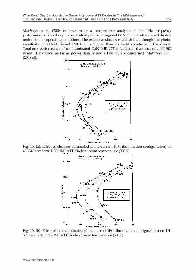
Wide Band Gap Semiconductor Based Highpower ATT Diodes In The MM-wave and THz Regime: Device Reliability, Experimental Feasibility and Photo-sensitivity 137
has been correlated with the relative ionization coefficients of charge carriers of SiC. The admittance characteristics and negative resistivity profiles of the un-illuminated and illuminated diodes are shown in Figures 13 and 14, respectively. The study reveals that the enhanced leakage current in illuminated devices, due to photo-illumination, degrades the output power density and negative resistance, but increases the tuning range of the devices. The optical illumination studies on the three types of SiC DDRs by Mukherjee et al. [Mukherjee et al (2008 b)] reveals that 4H-SiC based IMPATT is comparatively more photo-sensitive than its 6H- and 3C- counterparts. The photo-sensitivity of the 4H-SiC and 6H-SiC diodes at higher THz region (> 1 THz) are studied by Mukherjee et al. The admittance plots are shown in Figures 15 and 16. It is again found that in the higher THz region also, FC IMPATTs are more photo-sensitive than TM diodes. Compare to 4H-SiC IMPATT, 6H-SiC devices are found to be less promising in the THz region, as far as negative resistance, output power density, efficiencies and photo-sensitivity are concerned. However, it is worth mentioning that 6H-SiC based THz devices are definitely superior to conventional Si- and GaAs-based devices, since the latter categories of diodes could not reach the THz region. The effects of photo-illumination on the MM-wave and THz performances (Figures 17 and 18) of the GaN based diode are studied by Mukherjee et al. (2007 a) and (2009 b). The study reveals that negative conductance-GP of the diode decrease and at the same time, the frequency range over which the device exhibits negative conductance shifts towards higher frequencies with the increasing intensity of optical radiation. As expected, the upward shift in operating frequency is found to be more (~ 16 GHz) in case of the SLHL SDR IMPATT device. Illuminated FC diodes are found to be more photo-sensitive than their TM counterparts. The inequality in the magnitudes of electron and hole ionization rates in WZ-GaN have been found to be correlated with the above results. The study indicates GaN IMPATT is a promising photo-sensitive high power THz source.
Fig. 14. Effects of radiation on negative resistivity plots of SiC IMPATT diodes
Mukherjee et al. (2008 c) have made a comparative analysis of the THz frequency performances as well as photo-sensitivity of the hexagonal GaN and SiC (4H-) based diodes, under similar operating conditions. The extensive studies establish that, though the photo-sensitivity of 4H-SiC based IMPATT is higher than its GaN counterpart, the overall Terahertz performance of un-illuminated GaN IMPATT is far better than that of a 4H-SiC based THz device, as far as power density and efficiency are concerned [Mukherjee et al. (2008 c)].
Fig. 15. (a): Effect of electron dominated photo-current (TM illumination configuration) on 4H-SiC terahertz DDR IMPATT diode at room temperature (300K).
Fig. 15. (b): Effect of hole dominated photo-current (FC illumination configuration) on 4H-SiC terahertz DDR IMPATT diode at room temperature (300K).
www.intechopen.com

Advanced Microwave and Millimeter Wave Technologies: Semiconductor Devices, Circuits and Systems138
10. Experimental feasibility of new-class of WBG IMPATT diodes
Extensive studies, as discussed in previous section, have established the superiority of WBG IMPATT diodes as high power source at THz frequency regime. However, special efforts are required in the areas of GaN and SiC material growth, doping and device processing technologies, oscillator performance characterization, etc., before the full potential of GaN and SiC IMPATT diodes are utilized at THz region. Due to lack of any experimental data on WBG semiconductor based THz IMPATTs, the simulated results could not be compared. However, it is proposed that experimental validation of these results might be possible through the following steps.
Fig. 16. Effects of optical illumination on admittance plots of 6H-SiC based DDR IMPATT diode: (a-e = Junction temp. 300K), a‘-e‘=junction temperature T=500K).
Fig. 17. (a): Conductance (G) – Susceptance (B) plots of unilluminated GaN SDR IMPATT diode (a) and the illuminated diode (b-c) for different values of Mn.
Fig. 17. (b): Comductance (G) – Susceptance (B) platos of unilluminated GaN SDR IMPATT diode (a) and the illuminated diode (b-c) for different values of Mp.
Fig. 18. Conductance (G) – Susceptance (B) plots of unilluminated GaN flat profile SDR IMPATT diode (a) and the illuminated diode (b-d) for different values of Mn.
Fig. 19. Waveguide geometry: d=270 µm w=300.0 µm, and I=140.0mm Fabrication issues related to GaN IMPATT diode: (i) Growth of GaN p-n junction: GaN p-n junction can be obtained using metal organic chemical vapor deposition (MOCVD) technique and, to some extent, by molecular beam epitaxy (MBE). The most advanced results may be obtained by MOCVD technique, which
www.intechopen.com
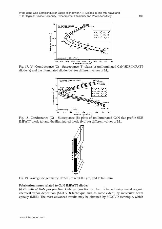
Wide Band Gap Semiconductor Based Highpower ATT Diodes In The MM-wave and THz Regime: Device Reliability, Experimental Feasibility and Photo-sensitivity 139
10. Experimental feasibility of new-class of WBG IMPATT diodes
Extensive studies, as discussed in previous section, have established the superiority of WBG IMPATT diodes as high power source at THz frequency regime. However, special efforts are required in the areas of GaN and SiC material growth, doping and device processing technologies, oscillator performance characterization, etc., before the full potential of GaN and SiC IMPATT diodes are utilized at THz region. Due to lack of any experimental data on WBG semiconductor based THz IMPATTs, the simulated results could not be compared. However, it is proposed that experimental validation of these results might be possible through the following steps.
Fig. 16. Effects of optical illumination on admittance plots of 6H-SiC based DDR IMPATT diode: (a-e = Junction temp. 300K), a‘-e‘=junction temperature T=500K).
Fig. 17. (a): Conductance (G) – Susceptance (B) plots of unilluminated GaN SDR IMPATT diode (a) and the illuminated diode (b-c) for different values of Mn.
Fig. 17. (b): Comductance (G) – Susceptance (B) platos of unilluminated GaN SDR IMPATT diode (a) and the illuminated diode (b-c) for different values of Mp.
Fig. 18. Conductance (G) – Susceptance (B) plots of unilluminated GaN flat profile SDR IMPATT diode (a) and the illuminated diode (b-d) for different values of Mn.
Fig. 19. Waveguide geometry: d=270 µm w=300.0 µm, and I=140.0mm Fabrication issues related to GaN IMPATT diode: (i) Growth of GaN p-n junction: GaN p-n junction can be obtained using metal organic chemical vapor deposition (MOCVD) technique and, to some extent, by molecular beam epitaxy (MBE). The most advanced results may be obtained by MOCVD technique, which
www.intechopen.com

Advanced Microwave and Millimeter Wave Technologies: Semiconductor Devices, Circuits and Systems140
includes the growth of GaN epitaxial layer from vapor phase. In this method, GaN may be grown from the vapor phase using metal organic gases as sources of Gallium and Nitrogen. For example, trimethylgallium (TMG) can be used as gallium source and Ammonia can be used as nitrogen source. Growth of GaN semiconductor may takes place in a reactor chamber on a substrate. During the growth, the substrate may be kept at growth temperature ranging from 800 to 1100° C. Single crystal wafers of Sapphire or SiC may serve as substrates for GaN deposition by MOCVD method. GaN THz device is found to be high power device. The large amount of current flowing in the device causes significant self-heating effect. If a very high quality GaN layer is grown on SiC substrate, SiC substrate will introduce the possibility of heat sink and that will result in a better heat-flow away from the active part of the diode. Using MOCVD process, thin layers (usually not thicker than 5 microns) of GaN can be grown on Sapphire or SiC substrates. In order to control the type of electrical conductivity in the grown material, electrically active impurities can be introduced in the reaction chamber during the growth. Undoped GaN layers usually exhibit n-type conductivity. The value of n-type conductivity can be controlled by introducing Si impurity (in form of SiH4 gas) in the reaction chamber during the growth. In order to obtain p-type GaN material by MOCVD method, Mg impurity can be introduced in the reactor chamber during the growth. Biscyclopentadienylmagnesium (Cp2 Mg) may be used as a Mg source for GaN doping. In order to form a n-p junction, at first, MOCVD growth process can be carried out using Si donor impurity, to form n-type layer of GaN on an n++ substrate, and after that p++-type cap layer can be grown on the n-layer by MOCVD process by doping high concentration of Mg impurity. However, MOCVD grown Mg-doped p++ layer, is highly resistive. In order to activate p-type conductivity, high temperature post-growth anneal in nitrogen atmosphere may be required. Since Mg requires large energy for ionization, in general, it is difficult to obtain heavily doped p++-type GaN with Mg. Beryllium (Be) may be used to achieve p++-type GaN, since the ionization energy of Be is low (~60 meV). Be-doped GaN layers may be obtained either by epitaxial growth methods, or by ion implantation. However, ion implantation may introduce severe lattice damage to the target material. Recently, Pastor et al (2007) assessed crystal damage of Be+-implanted GaN by UV Raman scattering and found a correlation between implantation dose and the extent of lattice damage caused to the target. The above mentioned procedure may be applied to form high quality GaN p-n junction. However, the MOCVD technology has a number of limitations: (1) This is expensive method requiring complicated growth equipment. In order to form GaN p-n junctions by MOCVD process, metal organic sources, for example TMG (Ga source) must be used. (2) Complicated chemical compounds have to be used as acceptor impurity sources, for example biscyclopentadienylmagnesium (Cp2 Mg) is usually used as a Mg-source. (3) In order to form high-quality GaN material on SiC substrates, MOCVD method requires to grow a buffer layer in-between SiC and GaN, which makes impossible to fabricate devices utilizing direct contact between SiC and GaN such as GaN/SiC p-n junction. Several experimental attempts have been taken to develop an alternative epitaxial growth technique to form GaN p-n junction. One method, which has been considered as a promising technique for the fabrication of GaN device structures, is hydride vapor phase
epitaxy (HVPE). The HVPE method is convenient for mass production of semiconductor devices due to its low cost, flexibility of growth conditions, and good reproducibility. In this method, Ga metal may be used as source material, thus HVPE technology does not require expensive source material. Furthermore, since these GaN layers can be grown directly on conducting SiC wafers without insulating buffer layers, diodes with n-GaN/p-SiC heterojunctions can be fabricated by HVPE. (ii) Formation of low resistive p++ and n++ ohmic contacts: Through photolithographic process, windows can be opened on p++ GaN layer for subsequent metal deposition. Using photolithography and lift-off techniques, low resistance contact metals, an alloy of Ni (20 nm)/Pd (20 nm) /Au (100 nm) [Chu et al (2000)], can be deposited inside the windows by an electron beam evaporator. The metal contacts should then be annealed in air, nitrogen and oxygen ambient conditions at different annealing temperatures ranging from 350 to 650 0C. The measurement of specific contact resistance may be done by circular Transmission Line Measurement (CTLM) system. A specific contact resistance of 1.0x10⁻⁴Ωcm2 can be achieved in this technique. If the similar metal composition is deposited on Be-implanted p++ type GaN layer with a carrier density of 8.1x1019 cm-3, without further annealing process, the sample will show good ohmic contact with a contact resistance of 4.5x10⁻⁶Ω cm2 [Chu et al (2000)]. A new metallization scheme has recently been developed for obtaining very low ohmic contact to n-GaN [Burm et al (1997)]. A composite metal layer Ti/Au/Ni/Au (150Å/2200 Å/400 Å/500 Å) can be deposited on n++-GaN. Following an annealing process at 9000C for 30s, a specific contact resistance (measured from TLM data) of 8.9x10⁻⁸ Ωcm2 for a doping density of 4x1017 cm-3 can be obtained [Burm et al (1997)]. (iii) Formation of diode mesa using Reactive Ion Etching (RIE): Effective etching techniques are useful for diode fabrication. GaN has very high bond energy (8.9 eV/atom) and a wide-bandgap, which makes it almost inert to bases and acids, which are low cost and highly available wet etchants, used in Si technology. There are various methods of dry etching involving sources of external energy to initiate and sustain the break up of the high-energy bonds in GaN. A few of the dry etching techniques used for GaN include, ion milling and reactive ion etching (RIE). Ion milling relies upon physical sputtering and is not very practical for GaN because of low etch rates and extreme damage to the material caused by the purely physical process. The RIE method is a better technique of dry etching because it involves chemical etching in addition to physical etching. The etch rates for GaN using RIE with various etch chemistries range from 17 to 100 nm/min [Adesidac et al. (1999)]. Wet etching is an important complement to dry etching methods by providing low damage etching, low cost, and complexity. Since conventional acids and bases cannot be used to etch nitrides, a recently developed technique called photo-electrochemical (PEC) wet etching is found to etch GaN with significantly high etch rates [Adesidac et al. (1999)]. The PEC process, utilizes photo-generated electron-hole pairs to enhance oxidation and reduction reactions taking place in an electrochemical cell. For the PEC etching, the etch rate of about 400 nm/min for KOH solution and about 40 nm/min for HCL solution can be obtained. PEC etching is highly anisotropic etching of GaN. It is a very effective technique for forming mesa structure for design of GaN IMPATT diode. (iv) On-Wafer DC Testing: After finishing the fabrication process, on-wafer DC testing should be performed before the diodes are packaged. DC testing will serve as the initial screening step of the device and the test results will be used for process evaluation.
www.intechopen.com

Wide Band Gap Semiconductor Based Highpower ATT Diodes In The MM-wave and THz Regime: Device Reliability, Experimental Feasibility and Photo-sensitivity 141
includes the growth of GaN epitaxial layer from vapor phase. In this method, GaN may be grown from the vapor phase using metal organic gases as sources of Gallium and Nitrogen. For example, trimethylgallium (TMG) can be used as gallium source and Ammonia can be used as nitrogen source. Growth of GaN semiconductor may takes place in a reactor chamber on a substrate. During the growth, the substrate may be kept at growth temperature ranging from 800 to 1100° C. Single crystal wafers of Sapphire or SiC may serve as substrates for GaN deposition by MOCVD method. GaN THz device is found to be high power device. The large amount of current flowing in the device causes significant self-heating effect. If a very high quality GaN layer is grown on SiC substrate, SiC substrate will introduce the possibility of heat sink and that will result in a better heat-flow away from the active part of the diode. Using MOCVD process, thin layers (usually not thicker than 5 microns) of GaN can be grown on Sapphire or SiC substrates. In order to control the type of electrical conductivity in the grown material, electrically active impurities can be introduced in the reaction chamber during the growth. Undoped GaN layers usually exhibit n-type conductivity. The value of n-type conductivity can be controlled by introducing Si impurity (in form of SiH4 gas) in the reaction chamber during the growth. In order to obtain p-type GaN material by MOCVD method, Mg impurity can be introduced in the reactor chamber during the growth. Biscyclopentadienylmagnesium (Cp2 Mg) may be used as a Mg source for GaN doping. In order to form a n-p junction, at first, MOCVD growth process can be carried out using Si donor impurity, to form n-type layer of GaN on an n++ substrate, and after that p++-type cap layer can be grown on the n-layer by MOCVD process by doping high concentration of Mg impurity. However, MOCVD grown Mg-doped p++ layer, is highly resistive. In order to activate p-type conductivity, high temperature post-growth anneal in nitrogen atmosphere may be required. Since Mg requires large energy for ionization, in general, it is difficult to obtain heavily doped p++-type GaN with Mg. Beryllium (Be) may be used to achieve p++-type GaN, since the ionization energy of Be is low (~60 meV). Be-doped GaN layers may be obtained either by epitaxial growth methods, or by ion implantation. However, ion implantation may introduce severe lattice damage to the target material. Recently, Pastor et al (2007) assessed crystal damage of Be+-implanted GaN by UV Raman scattering and found a correlation between implantation dose and the extent of lattice damage caused to the target. The above mentioned procedure may be applied to form high quality GaN p-n junction. However, the MOCVD technology has a number of limitations: (1) This is expensive method requiring complicated growth equipment. In order to form GaN p-n junctions by MOCVD process, metal organic sources, for example TMG (Ga source) must be used. (2) Complicated chemical compounds have to be used as acceptor impurity sources, for example biscyclopentadienylmagnesium (Cp2 Mg) is usually used as a Mg-source. (3) In order to form high-quality GaN material on SiC substrates, MOCVD method requires to grow a buffer layer in-between SiC and GaN, which makes impossible to fabricate devices utilizing direct contact between SiC and GaN such as GaN/SiC p-n junction. Several experimental attempts have been taken to develop an alternative epitaxial growth technique to form GaN p-n junction. One method, which has been considered as a promising technique for the fabrication of GaN device structures, is hydride vapor phase
epitaxy (HVPE). The HVPE method is convenient for mass production of semiconductor devices due to its low cost, flexibility of growth conditions, and good reproducibility. In this method, Ga metal may be used as source material, thus HVPE technology does not require expensive source material. Furthermore, since these GaN layers can be grown directly on conducting SiC wafers without insulating buffer layers, diodes with n-GaN/p-SiC heterojunctions can be fabricated by HVPE. (ii) Formation of low resistive p++ and n++ ohmic contacts: Through photolithographic process, windows can be opened on p++ GaN layer for subsequent metal deposition. Using photolithography and lift-off techniques, low resistance contact metals, an alloy of Ni (20 nm)/Pd (20 nm) /Au (100 nm) [Chu et al (2000)], can be deposited inside the windows by an electron beam evaporator. The metal contacts should then be annealed in air, nitrogen and oxygen ambient conditions at different annealing temperatures ranging from 350 to 650 0C. The measurement of specific contact resistance may be done by circular Transmission Line Measurement (CTLM) system. A specific contact resistance of 1.0x10⁻⁴Ωcm2 can be achieved in this technique. If the similar metal composition is deposited on Be-implanted p++ type GaN layer with a carrier density of 8.1x1019 cm-3, without further annealing process, the sample will show good ohmic contact with a contact resistance of 4.5x10⁻⁶Ω cm2 [Chu et al (2000)]. A new metallization scheme has recently been developed for obtaining very low ohmic contact to n-GaN [Burm et al (1997)]. A composite metal layer Ti/Au/Ni/Au (150Å/2200 Å/400 Å/500 Å) can be deposited on n++-GaN. Following an annealing process at 9000C for 30s, a specific contact resistance (measured from TLM data) of 8.9x10⁻⁸ Ωcm2 for a doping density of 4x1017 cm-3 can be obtained [Burm et al (1997)]. (iii) Formation of diode mesa using Reactive Ion Etching (RIE): Effective etching techniques are useful for diode fabrication. GaN has very high bond energy (8.9 eV/atom) and a wide-bandgap, which makes it almost inert to bases and acids, which are low cost and highly available wet etchants, used in Si technology. There are various methods of dry etching involving sources of external energy to initiate and sustain the break up of the high-energy bonds in GaN. A few of the dry etching techniques used for GaN include, ion milling and reactive ion etching (RIE). Ion milling relies upon physical sputtering and is not very practical for GaN because of low etch rates and extreme damage to the material caused by the purely physical process. The RIE method is a better technique of dry etching because it involves chemical etching in addition to physical etching. The etch rates for GaN using RIE with various etch chemistries range from 17 to 100 nm/min [Adesidac et al. (1999)]. Wet etching is an important complement to dry etching methods by providing low damage etching, low cost, and complexity. Since conventional acids and bases cannot be used to etch nitrides, a recently developed technique called photo-electrochemical (PEC) wet etching is found to etch GaN with significantly high etch rates [Adesidac et al. (1999)]. The PEC process, utilizes photo-generated electron-hole pairs to enhance oxidation and reduction reactions taking place in an electrochemical cell. For the PEC etching, the etch rate of about 400 nm/min for KOH solution and about 40 nm/min for HCL solution can be obtained. PEC etching is highly anisotropic etching of GaN. It is a very effective technique for forming mesa structure for design of GaN IMPATT diode. (iv) On-Wafer DC Testing: After finishing the fabrication process, on-wafer DC testing should be performed before the diodes are packaged. DC testing will serve as the initial screening step of the device and the test results will be used for process evaluation.
www.intechopen.com

Advanced Microwave and Millimeter Wave Technologies: Semiconductor Devices, Circuits and Systems142
(v)GaN IMPATT Device Packaging: The packaging should provide a low thermal resistance between the GaN diode chip and wave guide mount and should be mechanically rugged and hermetically sealed. The device can be bonded to a pill-type package. In pill-type configuration, the diode is bonded to a heat sink, which is usually gold plated. A ceramic or quartz ring encloses the diode and separates the heat sink from the package cap. Fabrication issues related to SiC IMPATT diode: SiC epiwafer (n++ substrate and n-type epilayer) can be procured from Cree Inc., Durham, NC, USA. The n-type doping is usually realized at Cree using nitrogen gas as the precursor. A SiC IMPATT device can be fabricated on the epiwafer following the process steps described below:
(i) Growth of p++ 4H-SiC layer: In order to assist p-type ohmic contact formation, the p++ 4H-SiC layer can be grown on top of the n-type film by Al2+ ion implantation; the doping concentration should be NA ≥ 2 x 1019 cm-3. The post-implantation annealing may be performed at ≈ 1600 º C for 45 minutes in argon atmosphere.
(ii) Formation of low resistive p++ and n++ contacts: The power dissipation of IMPATT devices strongly depend on the contact resistance. Following step (i), the samples may be cleaned by a “piranha” solution. After rinsing in DI water, the samples may be dipped in dilute hydrofluoric (HF) acid solution for 30 seconds and dried. Immediately after the cleaning, a SiO2 layer on the p++ side can be grown by Plasma Enhanced Chemical Vapor Deposition (PECVD) at 2850C. Through photolithographic process, windows can be opened inside the oxide layer. Using photolithography and lift-off techniques, contact metals (Al/Ti/Al) can then be deposited in the oxide windows by an electron beam evaporator. In order to obtain ohmic contacts the samples may be annealed for 3 minutes in a Rapid Thermal Anneal (RTA) furnace in nitrogen atmosphere at 950 0C. The post-deposition annealing at high temperature is generally preferred to reduce the specific contact resistance. As mentioned in the literature, Ni is the preferred material for ohmic contact on n-type SiC [Roccaforte et al (2006)]. Hence, for n++-type contact, a Ni layer of 200 nm thickness may be evaporated on the back-side (n++-side) of the wafer, followed by RTA treatment for 3 minutes at 950 0C. The choice of the metallic composition is based on the formation of Ni2Si alloy. As mentioned in several publications [Konishi et al (2003)], the higher the concentration of the Ni2Si in the contacts, the lower is the specific contact resistance. Finally, a composition of Ti/Au contact overlay is deposited on the p++-side by an electron beam evaporator. The specific contact resistance can be determined from transmission line measurement (TLM) data.
(iii) The oxide layer from the p++-side can then be removed by Buffered Oxide Etch (BOE).
(iv)Formation of diode mesa using Reactive Ion Etching (RIE): Si-C bonds show high chemical inertness, hence, wet etching is not efficient for reaching deep trenches. The more appropriate dry plasma etching, Reactive Ion Etching (RIE), may be used in separating diode mesa. Patterning of mesas may be carried out with photoresists: AZ 5214 (standard) and TI 35 ES (special photoresist for deep RIE Si etching) [Lazar et al (2006)]. A titanium/nickel (Ti/Ni) bilayer metal can be evaporated onto the sample. The metallic bilayer may be used as RIE mask that covers areas that will form mesa diodes. The dry etching can be performed in the Plasma Therm 790 reactor (say), an RIE reactor with a plasma (composed of SF6 and O2 gases) source generated at 13.56 MHz operating at a
maximum power of 300W. The depth and etch rate of the mask may be determined by profilometry measurements with a Tencor Alpha Step.
(v) On-Wafer DC Testing: After finishing the fabrication process, on-wafer DC testing are performed before the diodes are packaged. DC testing may serve as the initial screening step of the devices and the test results can be used for process evaluation.
(vi)SiC IMPATT Device Packaging: The packaging should provide a low thermal resistance between the SiC diode chip and wave guide mount and should be mechanically rugged and hermetically sealed. The device may be bonded to a pill-type package. The details of pill-type package are described earlier. C: Terahertz Transmission and Measurement: It is highly desirable that a THz transmission system should have low signal attenuation, low radiation loss, and high mode-confining property. Sommerfeld wires exhibit very low attenuation and dispersion, but suffers from large field extension into the surrounding medium. Moreover, it suffers from significant radiation loss at bendings. Metallic parallel plate waveguides, on the other hand, exhibit undistorted wave propagation of broadband sub-picosecond pulses even at bendings, but the propagating wave is confined in one transverse dimension giving rise to divergence loss. Transmission of THz signals from an IMPATT device may be possible with a dielectric coplanar wave guide, the device being an integral part of the waveguide. For THz (0.1-1 THz) signal transmission, a metallic slit waveguide, fabricated by sawing a 270 μm wide slit through a 140 mm wide and 300 μm thick silicon slabs may be used. The schematic diagram of waveguide is shown in Figure 19. The metallic slit waveguide shows dispersion less transmission of THz signals with very low attenuation. However, the residual edge roughness from wafer sawing [Wachter et al (2007)] can cause a small degree of radiation loss. For higher frequency (3 THz) power transfer, a ribbon-like structure fabricated from ceramic alumina may be utilized [Yeh et al (2005)]. The schematic diagrams of the structure are shown in Figures 20 (a-b). Measurements of THz power and frequency may be done with a THz VNA (Vector Network Analyzer) or, by employing Photoconductive Method. At Terahertz regime vector network measurements are challenging because of the reduced wavelength. Also, large phase errors resulting from temperature fluctuation can occur. In addition, flexing of the cable linking the scanning waveguide probe to the measurement equipment adds to the phase uncertainty. There are other systems for measurement and detection of THz signals for example Hot Electron Bolometer mixer- receiver and THz Time Domain Spectroscopy (THz-TDS). For detection and measurement of THz beam by photoconductive method, a THz-TDS set-up (Figure 21) may be used. The photoconductive setup can avoid the input and output coupling of free space Terahertz beams, giving rise to a compact and versatile setup. The details process was reported elsewhere [Yeh et al (2005)]. THz Time Domain Spectroscopy measurement (Figure 21) require multiple time delay scans, which is time consuming and can result in a systemic error caused by the intensity fluctuations of the THz beam. THz-TDS has smaller spectral range than Fourier Transform Spectroscopy (FTS) system and provide lower resolution than narrowband THz spectroscopy [Ferguson et al (2002)]. D: Proposed Experimental Scheme for Optical- Illumination of THz IMPATT Devices: In reality the diode under test may be mounted in a THz package, and can be sealed in ceramic sleeve with metallic contacts on each end. To expose the diode chip for illumination, a small groove can be cut in the ceramic sleeve. The diode package may be mounted in a
www.intechopen.com

Wide Band Gap Semiconductor Based Highpower ATT Diodes In The MM-wave and THz Regime: Device Reliability, Experimental Feasibility and Photo-sensitivity 143
(v)GaN IMPATT Device Packaging: The packaging should provide a low thermal resistance between the GaN diode chip and wave guide mount and should be mechanically rugged and hermetically sealed. The device can be bonded to a pill-type package. In pill-type configuration, the diode is bonded to a heat sink, which is usually gold plated. A ceramic or quartz ring encloses the diode and separates the heat sink from the package cap. Fabrication issues related to SiC IMPATT diode: SiC epiwafer (n++ substrate and n-type epilayer) can be procured from Cree Inc., Durham, NC, USA. The n-type doping is usually realized at Cree using nitrogen gas as the precursor. A SiC IMPATT device can be fabricated on the epiwafer following the process steps described below:
(i) Growth of p++ 4H-SiC layer: In order to assist p-type ohmic contact formation, the p++ 4H-SiC layer can be grown on top of the n-type film by Al2+ ion implantation; the doping concentration should be NA ≥ 2 x 1019 cm-3. The post-implantation annealing may be performed at ≈ 1600 º C for 45 minutes in argon atmosphere.
(ii) Formation of low resistive p++ and n++ contacts: The power dissipation of IMPATT devices strongly depend on the contact resistance. Following step (i), the samples may be cleaned by a “piranha” solution. After rinsing in DI water, the samples may be dipped in dilute hydrofluoric (HF) acid solution for 30 seconds and dried. Immediately after the cleaning, a SiO2 layer on the p++ side can be grown by Plasma Enhanced Chemical Vapor Deposition (PECVD) at 2850C. Through photolithographic process, windows can be opened inside the oxide layer. Using photolithography and lift-off techniques, contact metals (Al/Ti/Al) can then be deposited in the oxide windows by an electron beam evaporator. In order to obtain ohmic contacts the samples may be annealed for 3 minutes in a Rapid Thermal Anneal (RTA) furnace in nitrogen atmosphere at 950 0C. The post-deposition annealing at high temperature is generally preferred to reduce the specific contact resistance. As mentioned in the literature, Ni is the preferred material for ohmic contact on n-type SiC [Roccaforte et al (2006)]. Hence, for n++-type contact, a Ni layer of 200 nm thickness may be evaporated on the back-side (n++-side) of the wafer, followed by RTA treatment for 3 minutes at 950 0C. The choice of the metallic composition is based on the formation of Ni2Si alloy. As mentioned in several publications [Konishi et al (2003)], the higher the concentration of the Ni2Si in the contacts, the lower is the specific contact resistance. Finally, a composition of Ti/Au contact overlay is deposited on the p++-side by an electron beam evaporator. The specific contact resistance can be determined from transmission line measurement (TLM) data.
(iii) The oxide layer from the p++-side can then be removed by Buffered Oxide Etch (BOE).
(iv)Formation of diode mesa using Reactive Ion Etching (RIE): Si-C bonds show high chemical inertness, hence, wet etching is not efficient for reaching deep trenches. The more appropriate dry plasma etching, Reactive Ion Etching (RIE), may be used in separating diode mesa. Patterning of mesas may be carried out with photoresists: AZ 5214 (standard) and TI 35 ES (special photoresist for deep RIE Si etching) [Lazar et al (2006)]. A titanium/nickel (Ti/Ni) bilayer metal can be evaporated onto the sample. The metallic bilayer may be used as RIE mask that covers areas that will form mesa diodes. The dry etching can be performed in the Plasma Therm 790 reactor (say), an RIE reactor with a plasma (composed of SF6 and O2 gases) source generated at 13.56 MHz operating at a
maximum power of 300W. The depth and etch rate of the mask may be determined by profilometry measurements with a Tencor Alpha Step.
(v) On-Wafer DC Testing: After finishing the fabrication process, on-wafer DC testing are performed before the diodes are packaged. DC testing may serve as the initial screening step of the devices and the test results can be used for process evaluation.
(vi)SiC IMPATT Device Packaging: The packaging should provide a low thermal resistance between the SiC diode chip and wave guide mount and should be mechanically rugged and hermetically sealed. The device may be bonded to a pill-type package. The details of pill-type package are described earlier. C: Terahertz Transmission and Measurement: It is highly desirable that a THz transmission system should have low signal attenuation, low radiation loss, and high mode-confining property. Sommerfeld wires exhibit very low attenuation and dispersion, but suffers from large field extension into the surrounding medium. Moreover, it suffers from significant radiation loss at bendings. Metallic parallel plate waveguides, on the other hand, exhibit undistorted wave propagation of broadband sub-picosecond pulses even at bendings, but the propagating wave is confined in one transverse dimension giving rise to divergence loss. Transmission of THz signals from an IMPATT device may be possible with a dielectric coplanar wave guide, the device being an integral part of the waveguide. For THz (0.1-1 THz) signal transmission, a metallic slit waveguide, fabricated by sawing a 270 μm wide slit through a 140 mm wide and 300 μm thick silicon slabs may be used. The schematic diagram of waveguide is shown in Figure 19. The metallic slit waveguide shows dispersion less transmission of THz signals with very low attenuation. However, the residual edge roughness from wafer sawing [Wachter et al (2007)] can cause a small degree of radiation loss. For higher frequency (3 THz) power transfer, a ribbon-like structure fabricated from ceramic alumina may be utilized [Yeh et al (2005)]. The schematic diagrams of the structure are shown in Figures 20 (a-b). Measurements of THz power and frequency may be done with a THz VNA (Vector Network Analyzer) or, by employing Photoconductive Method. At Terahertz regime vector network measurements are challenging because of the reduced wavelength. Also, large phase errors resulting from temperature fluctuation can occur. In addition, flexing of the cable linking the scanning waveguide probe to the measurement equipment adds to the phase uncertainty. There are other systems for measurement and detection of THz signals for example Hot Electron Bolometer mixer- receiver and THz Time Domain Spectroscopy (THz-TDS). For detection and measurement of THz beam by photoconductive method, a THz-TDS set-up (Figure 21) may be used. The photoconductive setup can avoid the input and output coupling of free space Terahertz beams, giving rise to a compact and versatile setup. The details process was reported elsewhere [Yeh et al (2005)]. THz Time Domain Spectroscopy measurement (Figure 21) require multiple time delay scans, which is time consuming and can result in a systemic error caused by the intensity fluctuations of the THz beam. THz-TDS has smaller spectral range than Fourier Transform Spectroscopy (FTS) system and provide lower resolution than narrowband THz spectroscopy [Ferguson et al (2002)]. D: Proposed Experimental Scheme for Optical- Illumination of THz IMPATT Devices: In reality the diode under test may be mounted in a THz package, and can be sealed in ceramic sleeve with metallic contacts on each end. To expose the diode chip for illumination, a small groove can be cut in the ceramic sleeve. The diode package may be mounted in a
www.intechopen.com
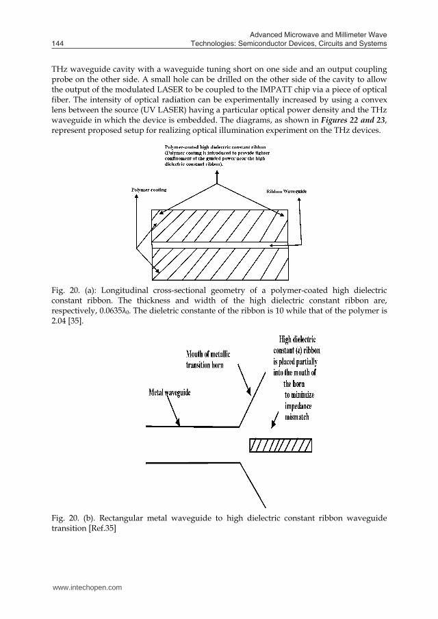
Advanced Microwave and Millimeter Wave Technologies: Semiconductor Devices, Circuits and Systems144
THz waveguide cavity with a waveguide tuning short on one side and an output coupling probe on the other side. A small hole can be drilled on the other side of the cavity to allow the output of the modulated LASER to be coupled to the IMPATT chip via a piece of optical fiber. The intensity of optical radiation can be experimentally increased by using a convex lens between the source (UV LASER) having a particular optical power density and the THz waveguide in which the device is embedded. The diagrams, as shown in Figures 22 and 23, represent proposed setup for realizing optical illumination experiment on the THz devices.
Fig. 20. (a): Longitudinal cross-sectional geometry of a polymer-coated high dielectric constant ribbon. The thickness and width of the high dielectric constant ribbon are, respectively, 0.0635λ0. The dieletric constante of the ribbon is 10 while that of the polymer is 2.04 [35].
Fig. 20. (b). Rectangular metal waveguide to high dielectric constant ribbon waveguide transition [Ref.35]
Fig. 21. Detection of Terahertz beam by photo-conductive method
Fig. 22. Experimental setup for optical illumination experiment on 4H-SiC IMPATT diode at THz region
www.intechopen.com

Wide Band Gap Semiconductor Based Highpower ATT Diodes In The MM-wave and THz Regime: Device Reliability, Experimental Feasibility and Photo-sensitivity 145
THz waveguide cavity with a waveguide tuning short on one side and an output coupling probe on the other side. A small hole can be drilled on the other side of the cavity to allow the output of the modulated LASER to be coupled to the IMPATT chip via a piece of optical fiber. The intensity of optical radiation can be experimentally increased by using a convex lens between the source (UV LASER) having a particular optical power density and the THz waveguide in which the device is embedded. The diagrams, as shown in Figures 22 and 23, represent proposed setup for realizing optical illumination experiment on the THz devices.
Fig. 20. (a): Longitudinal cross-sectional geometry of a polymer-coated high dielectric constant ribbon. The thickness and width of the high dielectric constant ribbon are, respectively, 0.0635λ0. The dieletric constante of the ribbon is 10 while that of the polymer is 2.04 [35].
Fig. 20. (b). Rectangular metal waveguide to high dielectric constant ribbon waveguide transition [Ref.35]
Fig. 21. Detection of Terahertz beam by photo-conductive method
Fig. 22. Experimental setup for optical illumination experiment on 4H-SiC IMPATT diode at THz region
www.intechopen.com

Advanced Microwave and Millimeter Wave Technologies: Semiconductor Devices, Circuits and Systems146
Fig. 23. Experimental setup for shining light on THz IMPATT diode
11. Conclusions
The prospects of WBG Wz-GaN and SiC (4H- and 6H-) based IMPATT devices of different structures and doping profiles were thoroughly examined both in the MM-wave and sub-millimeter wave (THz) region. The study established the potential of these WBG semiconductors in fabricating high-power and high-frequency IMPATT devices, in MM-wave as well as THz region. Si- based devices were also examined in these two regimes. The results showed that GaN and SiC based devices had superior performance over InP, in THz regime. A comparison of device properties of the 4H and 6H-SiC IMPATTs, revealed that the former is superior in terms of efficiency, output power generation capabilities and high temperature operation. Studies were also carried out on effects of parasitic series resistance and optical illumination effects due to photo-generated carriers in the designed TM and FC diodes. The effects of optical illumination on the different semiconductor (4H- and 6H- SiC, Wz-GaN) based diodes were examined for the two different illumination configurations: TM and FC. The results indicated that device negative resistance and Q-factor degraded, resulting in decrease of power density, along with an up-shift in the frequency of operation, due to the variation of incident illumination intensity. Moreover, it was observed that the predominant hole photo-current in FC illumination configuration, had more pronounced effect in modulating the high-frequency properties of illuminated SiC and GaN devices, while illuminated Si IMPATT showed opposite behavior. There is no doubt that, with the continuing progress in MM-wave and THz-device technology, the predictive simulation and proposed experimental feasibility of WBG semiconductor based IMPATT devices will become increasingly important for the success of research in modern high-power electronics.
12. References
Adesidac et al. (1999) “Dry and wet etching for group III nitrides”, MRS Internet J. Nitride Semiconductor Res.” 4S1, G1.4.
Adlerstein, M.G., Holway, L.H. ; Chu, S.L ; (1983)‘Measurement of series resistance in IMPATT diodes’, IEEE Trans. Electron Devices , vol. ED-30, pp. 179-182.
Alekseev, E ; and Pavlidis, D ; (2000) “GaN Gunn diodes for THz signal generation”, IEEE MTT-S International Microwave Symposium Digest., 2000, vol. 3, pp. 1905 – 1908.
Barbieri, S. et al. ; (2003) “Continuous-Wave Operation of Terahertz Quantum-Cascade Lasers,” IEEE J. Quantum Elec., vol. 39, no. 4, pp. 586–591.
Brandt, R. C. et al. ; (1998) « SiC for applications in high-power electronics”, in Semiconductors and Semimetals, Editor – Y. S. Park, New York, Academic, vol. 52, pp. 195 – 236.
Burm, J ; Chu, K ; Davis, W. A ; Schaff, W. J ; Eastman L. F ; and Eustis, T. J ; (1997)“Ultra-low resistive ohmic contacts on n-GaN using Si implantation”, Appl. Phys. Lett.,vol. 70, p.464.
Chao, Q. C. et al., (2009) “Generation of intense THz pulsed lasers pumped strongly by CO2 pulsed lasers”, Chinese Physics Letters, vol. 26, p. 064201.
Chu, C. F ; Yu, C. C ; Wang, Y. K ; Tsai, J. Y ; Lai, F. I ; and Wang, S. C ; (2000)“Low-resistance ohmic contacts on p-type GaN using Ni/Pd/Au metallization”, Appl. Phys. Lett. Vol. 77, pp. 3423-3425.
Dammertz, G ; et. al., (2002) “Development of a 140-GHz 1-MW Continuous Wave Gyrotron for the W7-X Stellarator,” IEEE Trans. Plasma Sci., vol. 30, no. 3,pp. 808–818.
Dobroiu, A. ; Yamashita, M ; Ohshima, Y. N. ; Morita, Y ; Otani, C ; and Kawase, K. ; (2004) “Terahertz imaging system based on a backward-wave-oscillator”, Applied Optics, vol. 43, p. 5637.
Dudley, M. ; Wang, S. ; Huang, W. ; Carter, Jr., C. H. and Fazi, C. ; (1995) J. Phys. D , vol. 28 pp. A63-A68.
Eisele, H. ; Naftaly, M. ; and Kamoua, R ; (2005) “Generation of submillimeter-wave radiation with GaAs TUNNETT diodes and InP Gunn devices in a second or higher harmonic mode,” Int. J. Infrared Millim. Waves, vol. 26, no. 1, pp.1–14.
Eisele, H. ; (2005) “355 GHz oscillator with GaAs TUNNETT diode,” Electron. Letts.,vol. 41, no. 6, pp. 55–56.
Elasser A. and Chow, T. P. (2002) “Silicon carbide benefits and advantages for power electronics circuits and systems,” Proceedings of the IEEE, vol. 90, no. 6, pp. 969–86.
Eisele, H and Haddad, G.I ; (1997) ‘Microwave Semiconductor Device Physics ‘, Ed. S. M. Sze, Wiley, New York, p. 343.
Ferguson B ; and Zhang, X ; (2002) “Materials for THz science and technology”, Nat. Matr, vol. 1, pp.26-33.
Flech, K ; Danly, G ; Jory, H. R. ; Kreischer,K. E. ; Lawson, W. ; Levush, B. and Temkin, R. J. (1999) “Characteristics and Applications of Fast-Wave Gyrodevices,” Proceedings of IEEE, vol. 87, no. 5, pp. 752–781.
Gummel, H.K. ; and Blue, J.L ; (1967) ‘A small signal theory of avalanche noise in IMPATT Diodes, IEEE Trans. Electron Devices’, vol. ED –14, pp. 569-580.
Ishibashi T. et al., (1977) “Liquid nitrogen cooled sub-millimeter wave Si IMPATT diodes”, Electronics Lett., vol. 13, p. 299.
www.intechopen.com
Wide Band Gap Semiconductor Based Highpower ATT Diodes In The MM-wave and THz Regime: Device Reliability, Experimental Feasibility and Photo-sensitivity 147
Fig. 23. Experimental setup for shining light on THz IMPATT diode
11. Conclusions
The prospects of WBG Wz-GaN and SiC (4H- and 6H-) based IMPATT devices of different structures and doping profiles were thoroughly examined both in the MM-wave and sub-millimeter wave (THz) region. The study established the potential of these WBG semiconductors in fabricating high-power and high-frequency IMPATT devices, in MM-wave as well as THz region. Si- based devices were also examined in these two regimes. The results showed that GaN and SiC based devices had superior performance over InP, in THz regime. A comparison of device properties of the 4H and 6H-SiC IMPATTs, revealed that the former is superior in terms of efficiency, output power generation capabilities and high temperature operation. Studies were also carried out on effects of parasitic series resistance and optical illumination effects due to photo-generated carriers in the designed TM and FC diodes. The effects of optical illumination on the different semiconductor (4H- and 6H- SiC, Wz-GaN) based diodes were examined for the two different illumination configurations: TM and FC. The results indicated that device negative resistance and Q-factor degraded, resulting in decrease of power density, along with an up-shift in the frequency of operation, due to the variation of incident illumination intensity. Moreover, it was observed that the predominant hole photo-current in FC illumination configuration, had more pronounced effect in modulating the high-frequency properties of illuminated SiC and GaN devices, while illuminated Si IMPATT showed opposite behavior. There is no doubt that, with the continuing progress in MM-wave and THz-device technology, the predictive simulation and proposed experimental feasibility of WBG semiconductor based IMPATT devices will become increasingly important for the success of research in modern high-power electronics.
12. References
Adesidac et al. (1999) “Dry and wet etching for group III nitrides”, MRS Internet J. Nitride Semiconductor Res.” 4S1, G1.4.
Adlerstein, M.G., Holway, L.H. ; Chu, S.L ; (1983)‘Measurement of series resistance in IMPATT diodes’, IEEE Trans. Electron Devices , vol. ED-30, pp. 179-182.
Alekseev, E ; and Pavlidis, D ; (2000) “GaN Gunn diodes for THz signal generation”, IEEE MTT-S International Microwave Symposium Digest., 2000, vol. 3, pp. 1905 – 1908.
Barbieri, S. et al. ; (2003) “Continuous-Wave Operation of Terahertz Quantum-Cascade Lasers,” IEEE J. Quantum Elec., vol. 39, no. 4, pp. 586–591.
Brandt, R. C. et al. ; (1998) « SiC for applications in high-power electronics”, in Semiconductors and Semimetals, Editor – Y. S. Park, New York, Academic, vol. 52, pp. 195 – 236.
Burm, J ; Chu, K ; Davis, W. A ; Schaff, W. J ; Eastman L. F ; and Eustis, T. J ; (1997)“Ultra-low resistive ohmic contacts on n-GaN using Si implantation”, Appl. Phys. Lett.,vol. 70, p.464.
Chao, Q. C. et al., (2009) “Generation of intense THz pulsed lasers pumped strongly by CO2 pulsed lasers”, Chinese Physics Letters, vol. 26, p. 064201.
Chu, C. F ; Yu, C. C ; Wang, Y. K ; Tsai, J. Y ; Lai, F. I ; and Wang, S. C ; (2000)“Low-resistance ohmic contacts on p-type GaN using Ni/Pd/Au metallization”, Appl. Phys. Lett. Vol. 77, pp. 3423-3425.
Dammertz, G ; et. al., (2002) “Development of a 140-GHz 1-MW Continuous Wave Gyrotron for the W7-X Stellarator,” IEEE Trans. Plasma Sci., vol. 30, no. 3,pp. 808–818.
Dobroiu, A. ; Yamashita, M ; Ohshima, Y. N. ; Morita, Y ; Otani, C ; and Kawase, K. ; (2004) “Terahertz imaging system based on a backward-wave-oscillator”, Applied Optics, vol. 43, p. 5637.
Dudley, M. ; Wang, S. ; Huang, W. ; Carter, Jr., C. H. and Fazi, C. ; (1995) J. Phys. D , vol. 28 pp. A63-A68.
Eisele, H. ; Naftaly, M. ; and Kamoua, R ; (2005) “Generation of submillimeter-wave radiation with GaAs TUNNETT diodes and InP Gunn devices in a second or higher harmonic mode,” Int. J. Infrared Millim. Waves, vol. 26, no. 1, pp.1–14.
Eisele, H. ; (2005) “355 GHz oscillator with GaAs TUNNETT diode,” Electron. Letts.,vol. 41, no. 6, pp. 55–56.
Elasser A. and Chow, T. P. (2002) “Silicon carbide benefits and advantages for power electronics circuits and systems,” Proceedings of the IEEE, vol. 90, no. 6, pp. 969–86.
Eisele, H and Haddad, G.I ; (1997) ‘Microwave Semiconductor Device Physics ‘, Ed. S. M. Sze, Wiley, New York, p. 343.
Ferguson B ; and Zhang, X ; (2002) “Materials for THz science and technology”, Nat. Matr, vol. 1, pp.26-33.
Flech, K ; Danly, G ; Jory, H. R. ; Kreischer,K. E. ; Lawson, W. ; Levush, B. and Temkin, R. J. (1999) “Characteristics and Applications of Fast-Wave Gyrodevices,” Proceedings of IEEE, vol. 87, no. 5, pp. 752–781.
Gummel, H.K. ; and Blue, J.L ; (1967) ‘A small signal theory of avalanche noise in IMPATT Diodes, IEEE Trans. Electron Devices’, vol. ED –14, pp. 569-580.
Ishibashi T. et al., (1977) “Liquid nitrogen cooled sub-millimeter wave Si IMPATT diodes”, Electronics Lett., vol. 13, p. 299.
www.intechopen.com

Advanced Microwave and Millimeter Wave Technologies: Semiconductor Devices, Circuits and Systems148
Ives, R. L ; Marsden, D. ; Caplan, M. ; Kory, C ; Neilson, J ; and Schwartzkopf, S ; (2003) “Advanced terahertz backward wave oscillators,” in 4th IEEE International Conference on Vacuum Electronics, pp. 20–21.
Johnston, R. L. ; De Loach, B. C ; Cohen, B. G, (1965) “A silicon diode microwave oscillator”, Bell. Syst. Tech. J., vol. 44, p. 369.
Karpowicz, N. ; Zhong, H. ; Zhang, C. ; Lin, K-I ; Hwang, J-S ; Xu, J ; and Zhang, X.-C. ; (2005) “Compact continuous-wave subterahertz system for inspection applications,” Appl. Phys. Lett., vol. 86, no. 5, pp. 54 105–3.
Keyes, R. W. ; (1973) “Silicon Carbide from the prospective of physical limits on semiconductor devices”, Proc. Silicon Carbide Conference: 1973, pp. 534 -542.
Konstantinov, A. O. ; Waheb, Q. ; Nordell N. ; and Lindefelt, U ; (1998) “Ionization rates and critical fields in 4H-SiC junction devices”, Mat. Sci. Forum, vol. 264 -268, pp. 513-515.
Konishi, R ; et al. (2003) “Development of Ni/Al and Ni/Ti/Al ohmic contact materials for p-type 4H-SiC” Mater. Sci. & Eng. B, vol. 98, pp. 286-293.
Krishnagopal, S ; and Kumar, V ; (2004) “Free-electron lasers,” Radiat. Phys. Chem., vol. 70, no. 4-5, pp. 559–569.
Kuzuhara, M. ; “Device technology based on new III-Nitride heterostructures”, Proc. CS MANTECH Conference, May 18th – 21st, 2009, Tampa, Florida, USA, 2009.
Lazar, M ; et al. (2006) “Deep SiC etching with RIE”, Supperlattices and Microstructures, vol. 40, pp. 388-392.
Leigh, M. A. et al ; (2009)“Narrowband pulsed THz source using eyesafe region fiber lasers and a non-linear crystal”, IEEE Photonics Technology Letters, vol. 21, no. 1, pp. 27-29.
Mazumder, N ; and Roy, S.K ; (1993) ‘Control of millimeter wave properties of high efficiency double drift region IMPATTs through enhancement of saturation current’, Phy.Status Solidi (a), vol. 137, pp. 267-275.
Mehdi, I ; Haddad G. I ; and Mains, R. K. ; (1998) “Microwave and millimeter-wave power generation in silicon carbide avalanche devices”, J. Appl. Phys., Vol. 64, No. 3, pp. 1533-1540.
Meng C. C. and Liao, G. R. (1998) “Analysis of SiC IMPATT device in Millimeter-Wave frequencies”, Microwave and Optical Technology Letters, vol. 18, p. 167.
Meng C. C. ; Liao G. R. ; and Chen, J. W. (1999) “Analysis of Millimeter-Wave GaN IMPATT oscillator at elevated temperature”, Microwave and Optical Technology Letters, vol. 23, p. 257.
Misawa, T ; (1966) “Negative resistance in p-n junctions under avalanche breakdown conditions: part II, IEEE Trans. Electron Dev., vol. ED-13, p. 143.
Mukherjee, M ; and Mazumder, N ; (2006), ‘Optically illuminated 4H-SiC THz IMPATT devices’, Egyptian J. of Solids, vol. 30, p. 85.
Mukherjee, M ; Mazumder, N ; Roy, S. K ; and Goswami, K ; (2007a) ‘GaN-IMPATT diode : a photo-sensitive high power THz source’, Semiconductor Science and Technology, vol. 22, p. 1258.
Mukherjee, M ; and Mazumder, N ; Dasgupta , A ; (2007 b), ‘Radiation effect on a high efficiency double drift region 4H-SiC Terahertz IMPATT diode’, Proceedings of IEEE 5th International Conference on Microwave and Millimeter Wave Technology (IEEE- ICMMT 2007), April 19 -22, 2007, Tsinghua University, Guilin, China, pp. 655-658.
Mukherjee, M ; Mazumder, N ; (2008 a) ‘Simulation experiment on optical modulation of 4H-SiC millimeter-wave high power IMPATT Oscillator”, Int. Journal of the European Microwave Association (EuMA Publishing - UK), vol. 4, 2008, pp. 276-282.
Mukherjee, M ; and Roy, S. K ; (2008b) ‘Design and Terahertz characteristics of hexagonal and cubic SiC based photo-irradiated IMPATT oscillators’, Proc. of IEEE Asia Pacific Microwave Conference 2008, IEEE-APMC 2008, Hong Kong, China, 16th – 19th December, 2008, China, Paper no. 1963.
Mukherjee, M ; Mazumder, N ;, Roy, S. K ; (2008 c), ‘Photosensitivity analysis of Gallium Nitride and Silicon Carbide Terahertz IMPATT oscillators: comparison of theoretical reliability and study on experimental feasibility’, IEEE Trans. Device and Materials Reliability, vol. 8, p. 608.
Mukherjee, M ; and Roy, S.K ; (2009b) ‘Optically modulated III-V Nitride based high-power IMPATT oscillator at MM-wave window frequency’, EuMA Int. J. Microwave and Wireless Technogy, accepted for publication.
Mukherjee, M ; Mazumder, N ; (2009) ‘Effect of charge-bump on high-frequency characteristics of α-SiC based double drift ATT diodes at MM-wave window frequencies”, J. IETE (India), vol. 55, p. 118.
Nagatsuma, T.; “Millimeter-Wave Photonic Technologies for Communications and Sensor Applications,” in New Photonics Technologies for the Information Age: The Dream of Ubiquitous Services, pp. 193–212, ed. by S. Sudo and K.Okamoto (Artech House, 2004).
Naftaly, M ; Foulds, A. P. ; Miles, R. E. and Davies, A. G. (2005) “Terahertz Transmission Spectroscopy of Nonpolar Materials and Relationship with Composition and Properties,” Int. J. Infrared Millim. Waves, vol. 26, no. 1, pp. 55–64.
Namordi, M. R. ; Coleman, D. J., (1980) ‘Design windows for low-high-low GaAs IMPATTs‘, IEEE Trans. Electron. Devices, vol. 27, p. 282.
Nishizawa, J.-I. ; Sasaki, T. ; Suto, K. ; Yamada, T. ; Tanabe, T. ; Tanno, T. ; Sawai, T. and Miura, Y. (2005) “THz imaging of nucleobases and cancerous tissue using a GaP THz-wave generator,” Opt. Commun., vol. 244, no. 1-6, pp. 469–474.
Ono, S ; Arai, M ; and Kimura, C ; (2005) “Demonstration of high power X-band oscillation in p+ n - n+ 4H-SiC IMPATT diodes with guard-ring termination”, Materials Science Forum, Vol. 981-984, pp. 483-485.
Orihashi, N. ; Suzuki S. and Asada, M. ; (2005) “One Terahertz harmonic oscillation of resonant tunneling Diodes”, Appl. Phys. Lett., vol. 87, p. 233501-1-3.
Panda, A. K. ; Pavlidis, D ; and Alekseev, E. A ; (2001) “Noise characteristics of GaN-based IMPATTs”, IEEE Trans. Electron Devices, vol. 48, pp.1473 -1475.
Pastor, D ; et al. (2007) “Crystal damage assessment of Be+-implanted GaN by UV Raman scattering”, Semicond. Sci. Tech., vol. 22, pp. 70-73, 2007 and references therein.
Pearton, S. J. ; Ren, F ; Zang A. P. and Lee, K. P. ; (2000) “Fabrication and performance of GaN electronic devices”, Materials Science and Engineering, vol. 250, pp. 1-158.
www.intechopen.com
Wide Band Gap Semiconductor Based Highpower ATT Diodes In The MM-wave and THz Regime: Device Reliability, Experimental Feasibility and Photo-sensitivity 149
Ives, R. L ; Marsden, D. ; Caplan, M. ; Kory, C ; Neilson, J ; and Schwartzkopf, S ; (2003) “Advanced terahertz backward wave oscillators,” in 4th IEEE International Conference on Vacuum Electronics, pp. 20–21.
Johnston, R. L. ; De Loach, B. C ; Cohen, B. G, (1965) “A silicon diode microwave oscillator”, Bell. Syst. Tech. J., vol. 44, p. 369.
Karpowicz, N. ; Zhong, H. ; Zhang, C. ; Lin, K-I ; Hwang, J-S ; Xu, J ; and Zhang, X.-C. ; (2005) “Compact continuous-wave subterahertz system for inspection applications,” Appl. Phys. Lett., vol. 86, no. 5, pp. 54 105–3.
Keyes, R. W. ; (1973) “Silicon Carbide from the prospective of physical limits on semiconductor devices”, Proc. Silicon Carbide Conference: 1973, pp. 534 -542.
Konstantinov, A. O. ; Waheb, Q. ; Nordell N. ; and Lindefelt, U ; (1998) “Ionization rates and critical fields in 4H-SiC junction devices”, Mat. Sci. Forum, vol. 264 -268, pp. 513-515.
Konishi, R ; et al. (2003) “Development of Ni/Al and Ni/Ti/Al ohmic contact materials for p-type 4H-SiC” Mater. Sci. & Eng. B, vol. 98, pp. 286-293.
Krishnagopal, S ; and Kumar, V ; (2004) “Free-electron lasers,” Radiat. Phys. Chem., vol. 70, no. 4-5, pp. 559–569.
Kuzuhara, M. ; “Device technology based on new III-Nitride heterostructures”, Proc. CS MANTECH Conference, May 18th – 21st, 2009, Tampa, Florida, USA, 2009.
Lazar, M ; et al. (2006) “Deep SiC etching with RIE”, Supperlattices and Microstructures, vol. 40, pp. 388-392.
Leigh, M. A. et al ; (2009)“Narrowband pulsed THz source using eyesafe region fiber lasers and a non-linear crystal”, IEEE Photonics Technology Letters, vol. 21, no. 1, pp. 27-29.
Mazumder, N ; and Roy, S.K ; (1993) ‘Control of millimeter wave properties of high efficiency double drift region IMPATTs through enhancement of saturation current’, Phy.Status Solidi (a), vol. 137, pp. 267-275.
Mehdi, I ; Haddad G. I ; and Mains, R. K. ; (1998) “Microwave and millimeter-wave power generation in silicon carbide avalanche devices”, J. Appl. Phys., Vol. 64, No. 3, pp. 1533-1540.
Meng C. C. and Liao, G. R. (1998) “Analysis of SiC IMPATT device in Millimeter-Wave frequencies”, Microwave and Optical Technology Letters, vol. 18, p. 167.
Meng C. C. ; Liao G. R. ; and Chen, J. W. (1999) “Analysis of Millimeter-Wave GaN IMPATT oscillator at elevated temperature”, Microwave and Optical Technology Letters, vol. 23, p. 257.
Misawa, T ; (1966) “Negative resistance in p-n junctions under avalanche breakdown conditions: part II, IEEE Trans. Electron Dev., vol. ED-13, p. 143.
Mukherjee, M ; and Mazumder, N ; (2006), ‘Optically illuminated 4H-SiC THz IMPATT devices’, Egyptian J. of Solids, vol. 30, p. 85.
Mukherjee, M ; Mazumder, N ; Roy, S. K ; and Goswami, K ; (2007a) ‘GaN-IMPATT diode : a photo-sensitive high power THz source’, Semiconductor Science and Technology, vol. 22, p. 1258.
Mukherjee, M ; and Mazumder, N ; Dasgupta , A ; (2007 b), ‘Radiation effect on a high efficiency double drift region 4H-SiC Terahertz IMPATT diode’, Proceedings of IEEE 5th International Conference on Microwave and Millimeter Wave Technology (IEEE- ICMMT 2007), April 19 -22, 2007, Tsinghua University, Guilin, China, pp. 655-658.
Mukherjee, M ; Mazumder, N ; (2008 a) ‘Simulation experiment on optical modulation of 4H-SiC millimeter-wave high power IMPATT Oscillator”, Int. Journal of the European Microwave Association (EuMA Publishing - UK), vol. 4, 2008, pp. 276-282.
Mukherjee, M ; and Roy, S. K ; (2008b) ‘Design and Terahertz characteristics of hexagonal and cubic SiC based photo-irradiated IMPATT oscillators’, Proc. of IEEE Asia Pacific Microwave Conference 2008, IEEE-APMC 2008, Hong Kong, China, 16th – 19th December, 2008, China, Paper no. 1963.
Mukherjee, M ; Mazumder, N ;, Roy, S. K ; (2008 c), ‘Photosensitivity analysis of Gallium Nitride and Silicon Carbide Terahertz IMPATT oscillators: comparison of theoretical reliability and study on experimental feasibility’, IEEE Trans. Device and Materials Reliability, vol. 8, p. 608.
Mukherjee, M ; and Roy, S.K ; (2009b) ‘Optically modulated III-V Nitride based high-power IMPATT oscillator at MM-wave window frequency’, EuMA Int. J. Microwave and Wireless Technogy, accepted for publication.
Mukherjee, M ; Mazumder, N ; (2009) ‘Effect of charge-bump on high-frequency characteristics of α-SiC based double drift ATT diodes at MM-wave window frequencies”, J. IETE (India), vol. 55, p. 118.
Nagatsuma, T.; “Millimeter-Wave Photonic Technologies for Communications and Sensor Applications,” in New Photonics Technologies for the Information Age: The Dream of Ubiquitous Services, pp. 193–212, ed. by S. Sudo and K.Okamoto (Artech House, 2004).
Naftaly, M ; Foulds, A. P. ; Miles, R. E. and Davies, A. G. (2005) “Terahertz Transmission Spectroscopy of Nonpolar Materials and Relationship with Composition and Properties,” Int. J. Infrared Millim. Waves, vol. 26, no. 1, pp. 55–64.
Namordi, M. R. ; Coleman, D. J., (1980) ‘Design windows for low-high-low GaAs IMPATTs‘, IEEE Trans. Electron. Devices, vol. 27, p. 282.
Nishizawa, J.-I. ; Sasaki, T. ; Suto, K. ; Yamada, T. ; Tanabe, T. ; Tanno, T. ; Sawai, T. and Miura, Y. (2005) “THz imaging of nucleobases and cancerous tissue using a GaP THz-wave generator,” Opt. Commun., vol. 244, no. 1-6, pp. 469–474.
Ono, S ; Arai, M ; and Kimura, C ; (2005) “Demonstration of high power X-band oscillation in p+ n - n+ 4H-SiC IMPATT diodes with guard-ring termination”, Materials Science Forum, Vol. 981-984, pp. 483-485.
Orihashi, N. ; Suzuki S. and Asada, M. ; (2005) “One Terahertz harmonic oscillation of resonant tunneling Diodes”, Appl. Phys. Lett., vol. 87, p. 233501-1-3.
Panda, A. K. ; Pavlidis, D ; and Alekseev, E. A ; (2001) “Noise characteristics of GaN-based IMPATTs”, IEEE Trans. Electron Devices, vol. 48, pp.1473 -1475.
Pastor, D ; et al. (2007) “Crystal damage assessment of Be+-implanted GaN by UV Raman scattering”, Semicond. Sci. Tech., vol. 22, pp. 70-73, 2007 and references therein.
Pearton, S. J. ; Ren, F ; Zang A. P. and Lee, K. P. ; (2000) “Fabrication and performance of GaN electronic devices”, Materials Science and Engineering, vol. 250, pp. 1-158.
www.intechopen.com
Advanced Microwave and Millimeter Wave Technologies: Semiconductor Devices, Circuits and Systems150
Read, W. T ; (1958)“A proposed high frequency negative resistance diode”, Bell. Syst. Tech. J., vol. 37, p. 401.
Reklaitis, A. ; and Reggiani, L. ; (2005) “Giant suppression of avalanche noise in GaN double drift impact diodes”, Solid-state Electronics, vol. 49, pp. 405 – 408.
Roccaforte, F ; et al. (2006) “SiC Materials and Devices; vol. 1, eds: M. Shur, S. Rumyantsev, and M. Levinshtein, World Scientific Publishing, p. 40, 2006.
Roy, S.K. ; M., Sridharan ; Ghosh , M ; and Pal B.B ; (1979) ‘Computer method for the dc field and carrier current profiles in the IMPATT device starting from the field extremum in the depletion layer’, Proc. 1st Conf. On Num Anal .Of Semiconductor Devices (NASECODE I) (Dublin: Boole) (Ed. J.H. Miller), p. 266.
Roy, S. K. ; Banerjee, J. P. and Pati, S. P; (1985) ”A Computer analysis of the distribution of high frequency negative resistance in the depletion layer of IMPATT Diodes”, Proc.4th Conf. on Num. Anal. of Semiconductor Devices (NASECODE IV) (Dublin) (Dublin: Boole), pp. 494-500.
Schmidt, L. P ; Biber, S ; Rehm, G ; and Huber, K ; (2002) “THz Measurement Technologies and applications,” 14th International Conference on Microwaves, Radar and Wireless Communications, vol. 2, pp. 581–587.
Shockley, W. ; (1954) “Negative resistance arising from transit time in semiconductor diode”, Bell. Syst. Tech. J, vol. 33, p. 799.
Vassilevski, K ; Zorenko, K ; (2001), “4H-SiC IMPATT diode fabrication and testing”, Tech. Digest of Int. Conf. on SiC and Related Materials- ICSCRM, Tsukuba, Japan, p. 713.
Wachter, M ; et al. (2007) “Metallic slit waveguide for dispersion-free low–loss terahertz signal transmission”, Applied Physics Letters, vol. 90, pp. 061111-061111-3.
Watanabe, Y ; Kawase, K ; Ikari, T ; Ito, H ; Ishikawa, Y ; and Minamide, H. (2004) “Component analysis of chemical mixtures using terahertz spectroscopic imaging,” Opt. Commun., vol. 234, no. 1-6, pp. 125–129.
Wang, S. ; Ferguson, B ; Abbott, D and Zhang, X.-C. (2003) “T-ray imaging and tomography,” J. Biol. Phys., vol. 29, no. 2-3, p. 247.
Yeh, C ; Shimabukuro, F ; and Siegel, P. H ; (2005) “Low-loss terahertz ribbon waveguides”, Applied Optics, vol.44, No.28, pp. 5937-5946.
Yuan, L ; Copper, J. A. ; Melloch M. R. ; and Webb, K. J. ; (2001) “Experimental demonstration of a Silicon Carbide IMPATT oscillator”, IEEE Electron Device Letters, vol. 22, pp. 266 -268.
Zhao, J. H. et al., (2000) “Monte Carlo simulation of 4H-SiC IMPATT diode”, Semicond. Sci. Technol., vol.15, pp.1093-1100.
www.intechopen.com
Advanced Microwave and Millimeter Wave TechnologiesSemiconductor Devices Circuits and SystemsEdited by Moumita Mukherjee
ISBN 978-953-307-031-5Hard cover, 642 pagesPublisher InTechPublished online 01, March, 2010Published in print edition March, 2010
InTech EuropeUniversity Campus STeP Ri Slavka Krautzeka 83/A 51000 Rijeka, Croatia Phone: +385 (51) 770 447 Fax: +385 (51) 686 166
InTech ChinaUnit 405, Office Block, Hotel Equatorial Shanghai No.65, Yan An Road (West), Shanghai, 200040, China
Phone: +86-21-62489820 Fax: +86-21-62489821
This book is planned to publish with an objective to provide a state-of-the-art reference book in the areas ofadvanced microwave, MM-Wave and THz devices, antennas and systemtechnologies for microwavecommunication engineers, Scientists and post-graduate students of electrical and electronics engineering,applied physicists. This reference book is a collection of 30 Chapters characterized in 3 parts: AdvancedMicrowave and MM-wave devices, integrated microwave and MM-wave circuits and Antennas and advancedmicrowave computer techniques, focusing on simulation, theories and applications. This book provides acomprehensive overview of the components and devices used in microwave and MM-Wave circuits, includingmicrowave transmission lines, resonators, filters, ferrite devices, solid state devices, transistor oscillators andamplifiers, directional couplers, microstripeline components, microwave detectors, mixers, converters andharmonic generators, and microwave solid-state switches, phase shifters and attenuators. Several applicationsarea also discusses here, like consumer, industrial, biomedical, and chemical applications of microwavetechnology. It also covers microwave instrumentation and measurement, thermodynamics, and applications innavigation and radio communication.
How to referenceIn order to correctly reference this scholarly work, feel free to copy and paste the following:
Moumita Mukherjee (2010). Wide Band Gap Semiconductor Based Highpower ATT Diodes In The MM-waveand THz Regime: Device Reliability, Experimental Feasibility and Photo-sensitivity, Advanced Microwave andMillimeter Wave Technologies Semiconductor Devices Circuits and Systems, Moumita Mukherjee (Ed.), ISBN:978-953-307-031-5, InTech, Available from: http://www.intechopen.com/books/advanced-microwave-and-millimeter-wave-technologies-semiconductor-devices-circuits-and-systems/wide-band-gap-semiconductor-based-highpower-att-diodes-in-the-mm-wave-and-thz-regime-device-reliabil
www.intechopen.com

www.intechopen.com

© 2010 The Author(s). Licensee IntechOpen. This chapter is distributedunder the terms of the Creative Commons Attribution-NonCommercial-ShareAlike-3.0 License, which permits use, distribution and reproduction fornon-commercial purposes, provided the original is properly cited andderivative works building on this content are distributed under the samelicense.


![Semiconductor Diodes [Demo]](https://img.pdfslide.net/doc/110x75/577d294d1a28ab4e1ea66956/semiconductor-diodes-demo.jpg)