Embed Size (px)
Citation preview
Wide-band lumped-element directional coupler withan arbitrary coupling coefficient
W.S. Tung and Y.C. Chiang
Abstract: A method of synthesising wide-band directional lumped-element couplers with anarbitrary coupling coefficient is presented. The proposed synthesis method can realise a co-directional type lumped-element coupler with a wider operational bandwidth than conventionaldesign methods while maintaining good amplitude and phase relationships of the output ports.Two coupler prototypes with coupling coefficients of 10 and 20dB are designed and fabricated toverify the design concept. The measurements are very close to the theoretical predictions.
1 Introduction
A Lange coupler is commonly used in the conventionalmicrowave integrated circuits (MICs) that are used toobtain the required circuit performance in balancedamplifiers and mixers. However, the Lange coupler consistsof several coupled quarter-wavelength microstrip lines, forMICs used at the lower end of the microwave band whichusually occupy a large chip area [1]. Thus, various methodsto design the lumped-element couplers in MICs ormonolithic MICs have been proposed [2–7]. Vogel pro-posed the design concept of realising a single-section orcascaded two-section ring-type coupler with an arbitrarycoupling coefficient for co-directional, contra-directionaland trans-directional couplers [3]. Recently, two methods ofsynthesising 3dB directional couplers with wide bandcharacteristics have been proposed [6–7]. Although thesynthetic technique in [7] can implement a two-sectionlumped coupler with a fractional bandwidth of about 42%,it is only applicable in realising a 3dB directional coupler;the operating frequency of the band is either below or abovethe designed frequency.
This study presents a synthesis method which extends [7].It is used to design a wide-band lumped-element couplerwith an arbitrary coupling coefficient. The design methodalso involves an algorithm to modify the values of same atthe elements previously obtained using a theoretical analysisin order to improve the return losses over a wider operatingbandwidth than the original bandwidth. This new set ofelements also ensures that the optimal operating band of thecoupler is near the designed frequency. In the proposeddesign method, a conventional even and odd half-circuitanalysis method will be used first to analyse the two-sectionlumped-element coupler. Then, a proposed set of designequations for synthesising a coupler with an arbitrarycoupling coefficient will be used to yield the values of theelements of the coupler. Finally, a set of modified values forthe elements will be obtained to improve the performance ofthe coupler.
A commercial microwave-circuit simulator will be usedto analyse the proposed couplers to verify the designconcept. Prototypes will be designed and fabricated on aconventional printed circuit board (PCB) substrate.
2 Synthetic method for the directional coupler
In developing the coupler synthesis method, a conventionaleven- and odd-mode analytical method is used to initially toanalyse the two-section lumped coupler shown in Fig. 1.The transmission matrices can then be derived for the even-and odd-mode half-circuits as follows:
Te;o
� �¼ T11e;o T12e;o
T21e;o T22e;o
� �
where the elements of the transmission matrices are:
T11e;o ¼1� 2XsBe;o 2� XsBe;o
� �þ j 1� XsBe;o
� �: XsY0 þ Be;oZ0 2� XsBe;o
� �� �ð1aÞ
T12e;o ¼ �j 1� XsBe;o
� �XsY0 � Be;oZ0 2� XsBe;o
� �� �ð1bÞ
T21e;o ¼ �T12e;o ð1cÞ
1
4
2
3
jXS
jXS jXS
jXS
jBpjBp
jBp jBp
jBmjBm
j2Bp
j2Bp
j2Bm
Fig. 1 Lumped-element directional coupler realised using coupledtwo-section p-networks
The authors are with the Institute and Department of Electronic Engineering,Chang Gung University, 259 Wen-Hwa 1st Road, Kwei-Shan, Tao-Yuan,Taiwan, ROC
r IEE, 2004
IEE Proceedings online no. 20040702
doi:10.1049/ip-map:20040702
Paper first received 29th October 2003 and in revised form 6th May 2004.Originally published online: 7th July 2004
IEE Proc.-Microw. Antennas Propag., Vol. 151, No. 4, August 2004 303
T22e;o ¼1� 2XsBe;o 2� XsBe;o
� �� j 1� XsBe;o
� �: XsY0 þ Be;oZ0 2� XsBe;o
� �� �ð1dÞ
and Be,o represent the admittances introduced by the shuntelements of even and odd half-circuits, and Be and Bo areequivalent to Bp and (Bp+2Bm), respectively.
According to the coupler design concept described in [3],a co-directional (i.e. S41¼ 0) coupler should have goodinput matching (S11¼ 0), and the following conditionshould be satisfied:
T12e ¼ T12o ¼ 0 ð2ÞSubstituting (1b) into (2), yields two solutions related to theelements of coupler:
XsBe;o ¼ 1 ð3Þand
XsY0 ¼ Be;oZ0ð2� XsBe;oÞ ð4ÞAssume that the desired phase difference between port 2and port 3 is 901 and that the power supplied to port 1 iscoupled to port 3 with a coupling coefficient C. Then S21
and S31 of the coupler can be taken as:
S21j j2þ S31j j2¼ 1 and yB ¼ yA þ ð2k þ 1Þ p2
k ¼ 0; �1; �2 � � � ð5aÞ
S21 ¼ffiffiffiffiffiffiffiffiffiffiffiffiffiffi1� C2p
ejyA S31 ¼ CejyB ð5bÞA set of equations, which extend the 3dB case reported in[7] to the case of an arbitrary coupling coefficient, is used torepresent T11e and T11o, which are:
T11e ¼ffiffiffiffiffiffiffiffiffiffiffiffiffiffi1� C2p
cos yA � C cos yB� � j
ffiffiffiffiffiffiffiffiffiffiffiffiffiffi1� C2p
sin yA � C sin yB�
ð6aÞ
T11o ¼ffiffiffiffiffiffiffiffiffiffiffiffiffiffi1� C2p
cos yA þ C cos yB� � j
ffiffiffiffiffiffiffiffiffiffiffiffiffiffi1� C2p
sin yA þ C sin yB�
ð6bÞ
Obviously, (6a) and (6b) satisfy the requirement shown in(5a) and (5b), and obeys the unitary principle for a losslessnetwork. The following equation also holds:
jT11ej2 ¼ jT11oj2 ¼ 1 ð7ÞSubstituting (3) or (4) into (1a) yields two probableequations for T11e,o:
T11e;o ¼ �1 ð8Þor
T11e;o ¼ 1� 2 XsY0ð Þ2þj2XsY0ð1� XsBe;oÞ ð9ÞSubstituting (8) or (9) to (6a) or (6b), yields four differentsituations in which the values of the elements can beobtained to realise a quadrature coupler with a couplingcoefficient C. These situations are discussed as follows:
Case 1: T11e,o¼�1.In this case, no difference exists between the even and
odd half-circuits, this result contradicts that obtained forpractical half-circuits using the even- and odd-modeexcitations. Therefore, no valid solution can be found.
Case 2: T11e;o ¼ 1� 2 XsY0ð Þ2þj2XsY0ð1� XsBe;oÞ.In this case, the real part of T11 for both the even-
and odd-mode half-circuits must be the same, so T11e andT11o are the complex conjugate of each other. Thus, yA and
yB in (6a) and (6b) should be:
yA ¼np yB ¼ yA þ ð2nþ 1Þ p2
n ¼0; �1; �2; � � �to satisfy such a requirement, so (6) can be simplified to:
T11e ¼ �ffiffiffiffiffiffiffiffiffiffiffiffiffiffi1� C2p
� jC ð10Þ
T11o ¼ �ffiffiffiffiffiffiffiffiffiffiffiffiffiffi1� C2p
� jC ð11ÞSubstituting (10) and (11) to (9), yields three equations forXs, Bm and Bp in Fig. 1. The values of the elements derivedfrom the previous equations are:
Xs ¼ �Z0
ffiffiffiffiffiffiffiffiffiffiffiffiffiffiffiffiffiffiffiffiffiffiffiffiffiffi1�
ffiffiffiffiffiffiffiffiffiffiffiffiffiffi1� C2p
2
s
Bm ¼ �C= 2X 2s Y0
� �and
Bp ¼ 2XsY0 � Cð Þ= 2X 2s Y0
� �
Case 3: T11e¼�1 and T11o ¼ 1� 2 XsY0ð Þ2þj2XsY0 �ð1� XsBoÞ.
In this case, Be¼ 1/Xs is obtained from T11e¼�1, andT11o in (6b) equals:
T11o ¼ 1þ 2ffiffiffiffiffiffiffiffiffiffiffiffiffiffi1� C2p
cos yA
� j 2ffiffiffiffiffiffiffiffiffiffiffiffiffiffi1� C2p
sin yA�
ð12Þ
According to the unitary principle, the magnitude of (12)must be unity, so an equation relating to the couplingcoefficient and the phase can be obtained as:
cos yA ¼ �ffiffiffiffiffiffiffiffiffiffiffiffiffiffi1� C2p
ð13Þand T11o can be rewritten as:
T11o ¼ 2C2 � 1� �
� j 2Cffiffiffiffiffiffiffiffiffiffiffiffiffiffi1� C2p�
ð14Þ
Substituting (14) to (9), yields the other set of equations fordetermining the values of the elements. Thus, in this case thevalues of the elements:
Xs ¼ffiffiffiffiffiffiffiffiffiffiffiffiffiffi1� C2p�
Z0 or � ðffiffiffiffiffiffiffiffiffiffiffiffiffiffi1� C2p
ÞZ0
Bm ¼� Y0Cð Þ= 2ffiffiffiffiffiffiffiffiffiffiffiffiffiffi1� C2p�
or � Y0Cð Þ= 2ffiffiffiffiffiffiffiffiffiffiffiffiffiffi1� C2p�
Bp ¼Y0=ffiffiffiffiffiffiffiffiffiffiffiffiffiffi1� C2p
or � Y0=ffiffiffiffiffiffiffiffiffiffiffiffiffiffi1� C2p
Case 4: T11o¼�1; T11e ¼ 1� 2 XsY0ð Þ2þj2XsY0 �ð1� XsBeÞ.
A similar design procedure to that in case 3, but withswitched equations for even- and odd-mode half-circuits,yields the following values for the elements in realisingcoupler with a coupling coefficient of C:
Xs ¼ffiffiffiffiffiffiffiffiffiffiffiffiffiffi1� C2p�
Z0 or �ffiffiffiffiffiffiffiffiffiffiffiffiffiffi1� C2p�
Z0
Bm ¼� Y0Cð Þ= 2ffiffiffiffiffiffiffiffiffiffiffiffiffiffi1� C2p�
or � Y0Cð Þ= 2ffiffiffiffiffiffiffiffiffiffiffiffiffiffi1� C2p�
Bp ¼ 1� Cð ÞY0=ffiffiffiffiffiffiffiffiffiffiffiffiffiffi1� C2p
or � 1� Cð ÞY0=ffiffiffiffiffiffiffiffiffiffiffiffiffiffi1� C2p
The previous analysis results yielded three sets of values forthe elements to realise the coupler. A commercial micro-wave-circuit simulator, Ansoft Serenade, is applied toevaluate the performances of the couplers realised usingthese three sets of elements. The elements obtained in case 2are the same as those reported in [3] and those in cases 3
304 IEE Proc.-Microw. Antennas Propag., Vol. 151, No. 4, August 2004
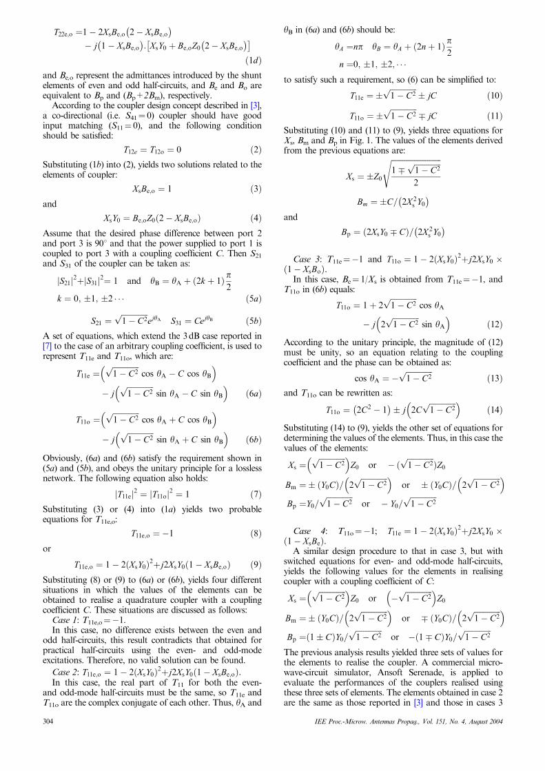
and 4 are the same results as in [7] for a coupler with a 3 dBcoupling coefficient. Circles and squares in Fig. 2 representthe computer-simulated input return losses of the 3dBcouplers realised using the elements obtained in cases 3 and4, respectively. As shown, these couplers indeed demon-strate wide band characteristics, but the optimal operatingbands are above and below the designed frequency of 1.0f0.
Inspecting the values of the element derived from cases 3and 4 reveals that the values, with the exception Bp, are thesame, possibly implying that these values, reveal a strongperformance of a coupler over a wide frequency region,such as from 0.75f0 to 1.45f0, as depicted in Fig. 2.Therefore, the values of Xs and Bm are fixed to those incases 3 and 4, and the value of Bp is changed to observeany performance variation of the coupler. The values
of Bp namely: �Y0=ffiffiffiffiffiffiffiffiffiffiffiffiffiffi1� C2p
and � 1� Cð ÞY0=ffiffiffiffiffiffiffiffiffiffiffiffiffiffi1� C2p
,represent the lower and upper bounds for implementing thecoupler. When Bp falls outside this range, the operatingbandwidth of the coupler is decreased. When the value ofBp is varied within this range, the operating bandwidth andinput return loss vary accordingly. The optimum solutionfor realising the coupler is that Bp is the arithmetic mean of
�Y0=ffiffiffiffiffiffiffiffiffiffiffiffiffiffi1� C2p
and � 1� Cð ÞY0=ffiffiffiffiffiffiffiffiffiffiffiffiffiffi1� C2p
. The triangles inFig. 2 represent the coupler’s input return loss realised bysuch a set of elements; the operating bandwidth is alsoindicated. As shown, the coupler that is realised using theoptimum set of elements has a 5% better operating band-width than that in case 3. Although the operating band-width is almost the same as in case 4, better return losses areobtained in the designed operating band. The optimal ope-rating band of the coupler realised using the new element setis near the designed frequency, thereby increasing the caseof design for the practical circuit of the coupler.
However, the values of all but one of the elementsdescribed in the previous three different cases remain fixedas the coupling coefficient C is decreased, resulting in anarrow band and characteristics. Thus, the proposedcoupler design method will be more useful in designinga weakly coupled structures. Two prototypes with 10 and20dB couplings will now be used to verify the proposedsynthetic method.
3 Experimental results
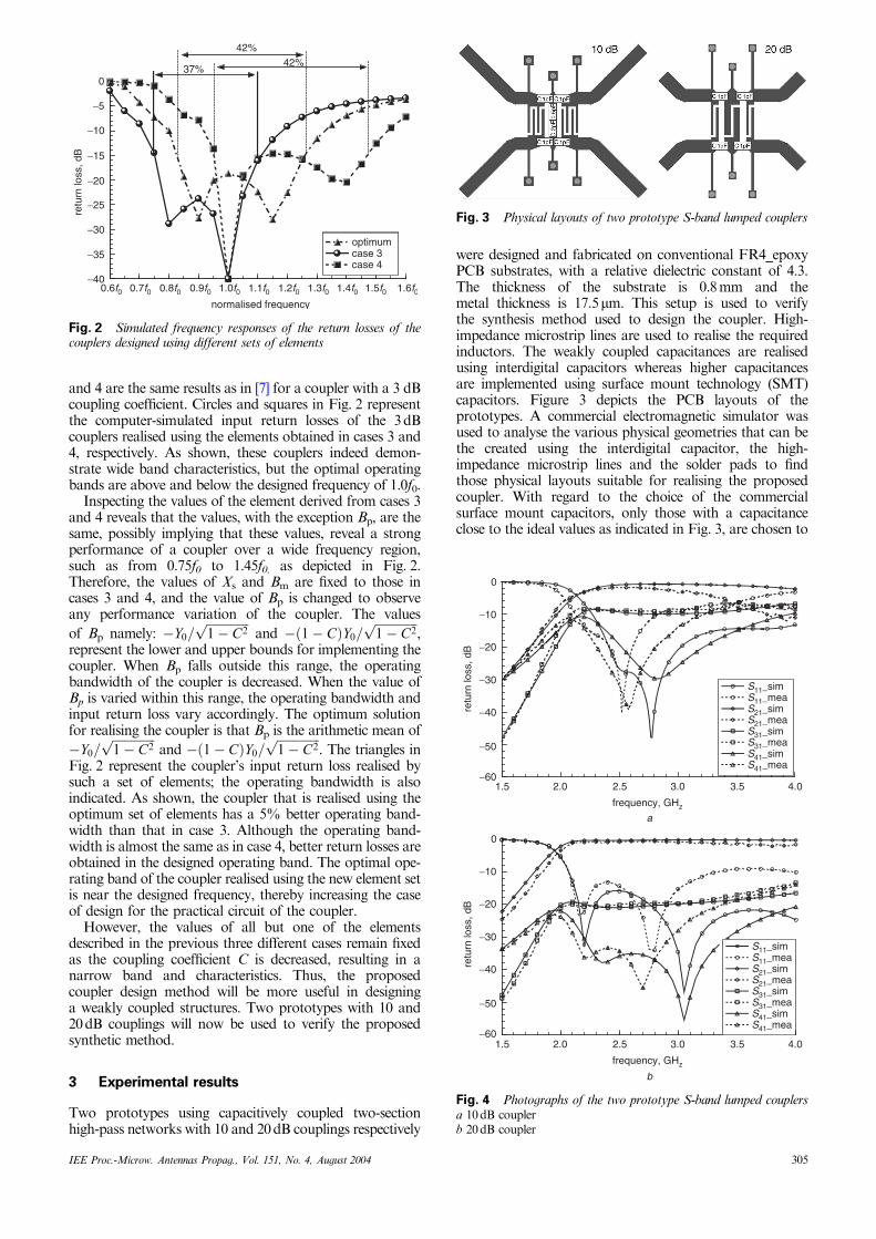
Two prototypes using capacitively coupled two-sectionhigh-pass networks with 10 and 20dB couplings respectively
were designed and fabricated on conventional FR4_epoxyPCB substrates, with a relative dielectric constant of 4.3.The thickness of the substrate is 0.8mm and themetal thickness is 17.5mm. This setup is used to verifythe synthesis method used to design the coupler. High-impedance microstrip lines are used to realise the requiredinductors. The weakly coupled capacitances are realisedusing interdigital capacitors whereas higher capacitancesare implemented using surface mount technology (SMT)capacitors. Figure 3 depicts the PCB layouts of theprototypes. A commercial electromagnetic simulator wasused to analyse the various physical geometries that can bethe created using the interdigital capacitor, the high-impedance microstrip lines and the solder pads to findthose physical layouts suitable for realising the proposedcoupler. With regard to the choice of the commercialsurface mount capacitors, only those with a capacitanceclose to the ideal values as indicated in Fig. 3, are chosen to
0.6f0 0.7f0 0.8f0 0.9f0 1.0f0 1.1f0 1.2f0 1.3f0 1.4f0 1.5f0 1.6f0normalised frequency
−10
−15
−20
−25
−30
−35
−40
−5
0re
turn
loss
, dB
optimumcase 3case 4
37%
42%42%
Fig. 2 Simulated frequency responses of the return losses of thecouplers designed using different sets of elements
Fig. 3 Physical layouts of two prototype S-band lumped couplers
S11_simS11_meaS21_simS21_meaS31_simS31_meaS41_simS41_mea
1.5 2.0 2.5 3.0 3.5 4.0
frequency, GHz
1.5 2.0 2.5 3.0 3.5 4.0
frequency, GHz
−10
−20
−30
−40
−50
−60
0
retu
rn lo
ss, d
B
−10
−20
−30
−40
−50
−60
0
retu
rn lo
ss, d
B
S11_simS11_meaS21_simS21_meaS31_simS31_meaS41_simS41_mea
a
b
Fig. 4 Photographs of the two prototype S-band lumped couplersa 10dB couplerb 20dB coupler
IEE Proc.-Microw. Antennas Propag., Vol. 151, No. 4, August 2004 305
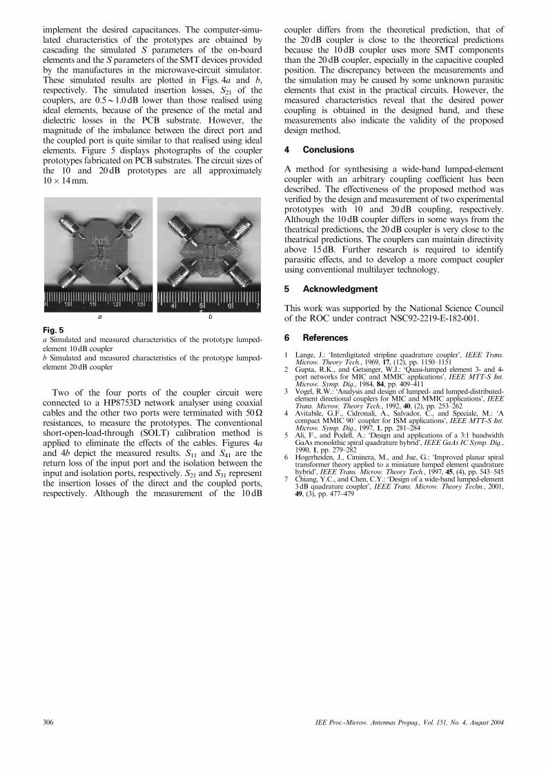
implement the desired capacitances. The computer-simu-lated characteristics of the prototypes are obtained bycascading the simulated S parameters of the on-boardelements and the S parameters of the SMT devices providedby the manufactures in the microwave-circuit simulator.These simulated results are plotted in Figs. 4a and b,respectively. The simulated insertion losses, S21 of thecouplers, are 0.5B1.0dB lower than those realised usingideal elements, because of the presence of the metal anddielectric losses in the PCB substrate. However, themagnitude of the imbalance between the direct port andthe coupled port is quite similar to that realised using idealelements. Figure 5 displays photographs of the couplerprototypes fabricated on PCB substrates. The circuit sizes ofthe 10 and 20dB prototypes are all approximately10� 14mm.
Two of the four ports of the coupler circuit wereconnected to a HP8753D network analyser using coaxialcables and the other two ports were terminated with 50Oresistances, to measure the prototypes. The conventionalshort-open-load-through (SOLT) calibration method isapplied to eliminate the effects of the cables. Figures 4aand 4b depict the measured results. S11 and S41 are thereturn loss of the input port and the isolation between theinput and isolation ports, respectively. S21 and S31 representthe insertion losses of the direct and the coupled ports,respectively. Although the measurement of the 10dB
coupler differs from the theoretical prediction, that ofthe 20dB coupler is close to the theoretical predictionsbecause the 10dB coupler uses more SMT componentsthan the 20dB coupler, especially in the capacitive coupledposition. The discrepancy between the measurements andthe simulation may be caused by some unknown parasiticelements that exist in the practical circuits. However, themeasured characteristics reveal that the desired powercoupling is obtained in the designed band, and thesemeasurements also indicate the validity of the proposeddesign method.
4 Conclusions
A method for synthesising a wide-band lumped-elementcoupler with an arbitrary coupling coefficient has beendescribed. The effectiveness of the proposed method wasverified by the design and measurement of two experimentalprototypes with 10 and 20dB coupling, respectively.Although the 10dB coupler differs in some ways from thetheatrical predictions, the 20dB coupler is very close to thetheatrical predictions. The couplers can maintain directivityabove 15dB. Further research is required to identifyparasitic effects, and to develop a more compact couplerusing conventional multilayer technology.
5 Acknowledgment
This work was supported by the National Science Councilof the ROC under contract NSC92-2219-E-182-001.
6 References
1 Lange, J.: ‘Interdigitated stripline quadrature coupler’, IEEE Trans.Microw. Theory Tech., 1969, 17, (12), pp. 1150–1151
2 Gupta, R.K., and Getsinger, W.J.: ‘Quasi-lumped element 3- and 4-port networks for MIC and MMIC applications’, IEEE MTT-S Int.Microw. Symp. Dig., 1984, 84, pp. 409–411
3 Vogel, R.W.: ‘Analysis and design of lumped- and lumped-distributed-element directional couplers for MIC and MMIC applications’, IEEETrans. Microw. Theory Tech., 1992, 40, (2), pp. 253–262
4 Avitabile, G.F., Cidronali, A., Salvador, C., and Speciale, M.: ‘Acompact MMIC 901 coupler for ISM applications’, IEEE MTT-S Int.Microw. Symp. Dig., 1997, 1, pp. 281–284
5 Ali, F., and Podell, A.: ‘Design and applications of a 3:1 bandwidthGaAs monolithic spiral quadrature hybrid’, IEEE GaAs IC Symp. Dig.,1990, 1, pp. 279–282
6 Hogerheiden, J., Ciminera, M., and Jue, G.: ‘Improved planar spiraltransformer theory applied to a miniature lumped element quadraturehybrid’, IEEE Trans. Microw. Theory Tech., 1997, 45, (4), pp. 543–545
7 Chiang, Y.C., and Chen, C.Y.: ‘Design of a wide-band lumped-element3dB quadrature coupler’, IEEE Trans. Microw. Theory Techn., 2001,49, (3), pp. 477–479
Fig. 5a Simulated and measured characteristics of the prototype lumped-element 10dB couplerb Simulated and measured characteristics of the prototype lumped-element 20dB coupler
306 IEE Proc.-Microw. Antennas Propag., Vol. 151, No. 4, August 2004