Embed Size (px)
Citation preview

Wide Bandgap Semiconductors for Microwave Power Devices
Dr. C. E. Weitzel Consultant: Wide Bandgap Power Devices

Presentation Outline
• Why Wide Bandgap Semiconductors?
• SiC Microwave Power Devices
• What are FET Field‐Plates?
• AlGaN/GaN Microwave Power Devices

The Rest of the Wide Bandgap story
• SiC produced the first commercial BLUE LED’s • GaN produced first high brightness BLUE LED’s • GaN based materials enabled and dominate the LED commercial market • Low intrinsic carrier concentraKon enables significantly higher operaKng temperatures • GaN‐on‐Si looks promising for Switching Power
Devices to compete with silicon IGBT’s, silicon MOSFET’s, and SiC MOSFET’s.

Why Wide Bandgap Semiconductors?
B. Ozpineci and L.M. Tolbert, “Comparison of Wide‐Bandgap Semiconductors for Power Electronic ApplicaKons,” Oak Ridge NaKonal Laboratory, December 12, 2003
RelaKve Cost $ $$ $$$$$ $$$$$ $$$$ $$$$$$$$$$

• Wide bandgap enables high breakdown voltages • This enables a tradeoff between operaKng voltage and
current, but in either case boosts power handling capability B. Ozpineci and L.M. Tolbert, “Comparison of Wide‐Bandgap Semiconductors for Power Electronic ApplicaKons,” Oak Ridge NaKonal Laboratory, December 12, 2003
Diode Breakdown Voltages
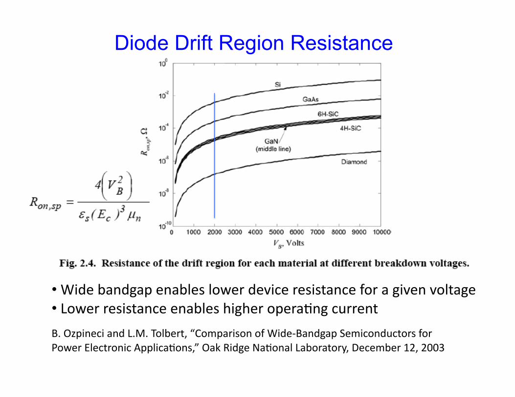
• Wide bandgap enables lower device resistance for a given voltage • Lower resistance enables higher operaKng current B. Ozpineci and L.M. Tolbert, “Comparison of Wide‐Bandgap Semiconductors for Power Electronic ApplicaKons,” Oak Ridge NaKonal Laboratory, December 12, 2003
Diode Drift Region Resistance
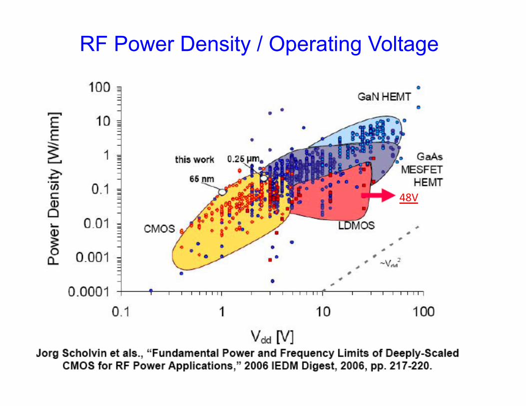
RF Power Density / Operating Voltage
48V

Micropipes Result from Screw Dislocation

Reduction of Micropipe Density / Wafer Size

Very Low Micropipe Density SiC Wafer

SiC MESFET --- the first wide bandgap
microwave power transistor
SiC MESFET’s, SiC MOSFET’s & SiC SIT’s


Probably Highest SiC MESFET power density ever reported I would certainly like to know more details about this device


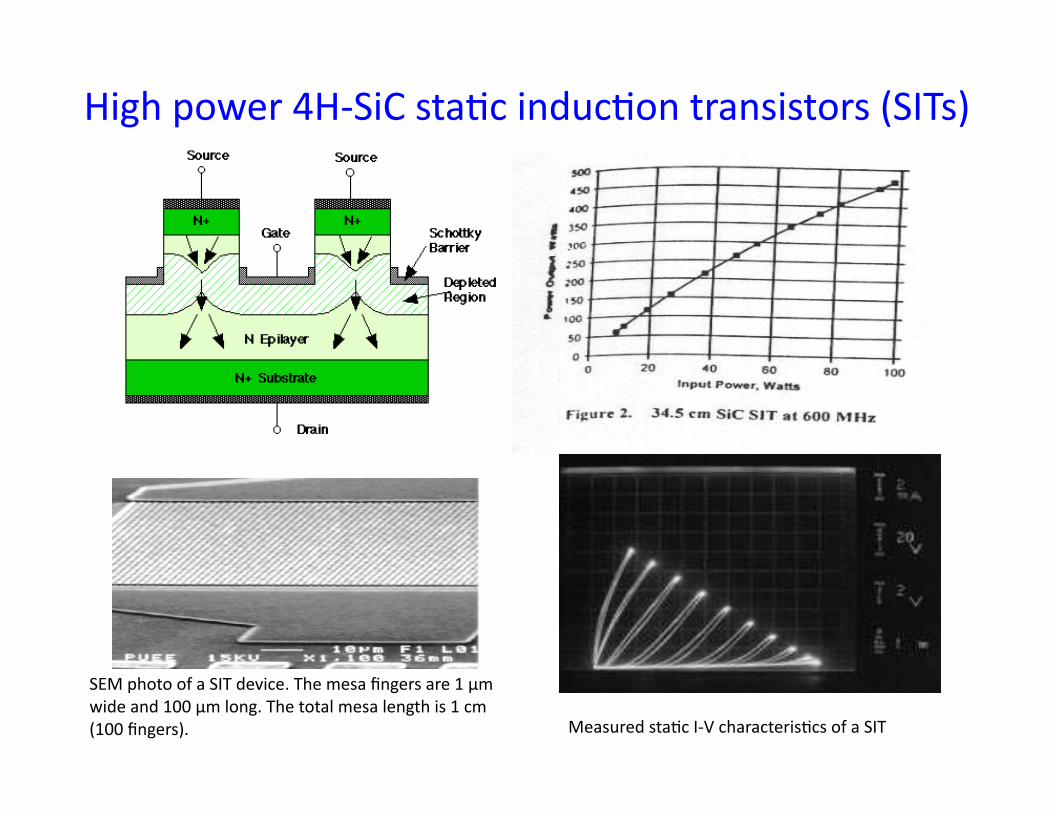
High power 4H‐SiC staKc inducKon transistors (SITs)
Measured staKc I‐V characterisKcs of a SIT
SEM photo of a SIT device. The mesa fingers are 1 µm wide and 100 µm long. The total mesa length is 1 cm (100 fingers).

Microsemi introduced a 2.2kW SiC SIT in Sept. 2010

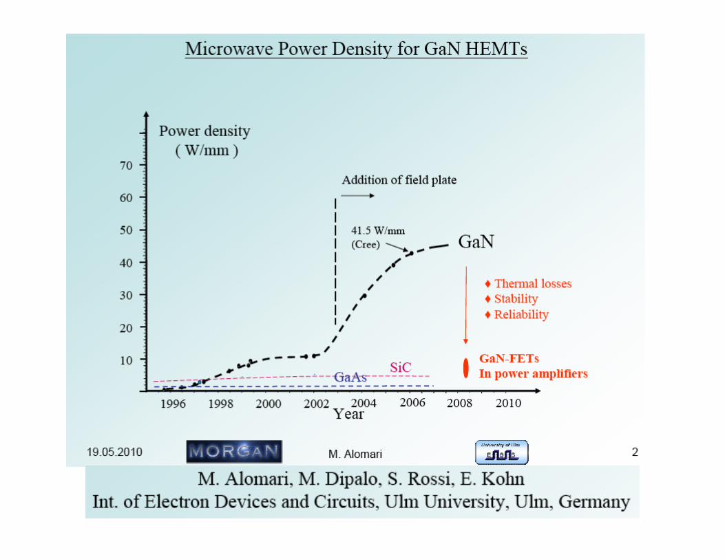
What are Field-Plates? aka - Step-Gates, Faraday Shields,
Source connected Field-Plates
Field‐plate is a metal structure added to a FET between the gate and drain that increases the microwave gain and/or breakdown voltage (Si, GaAs, SiC, GaN).
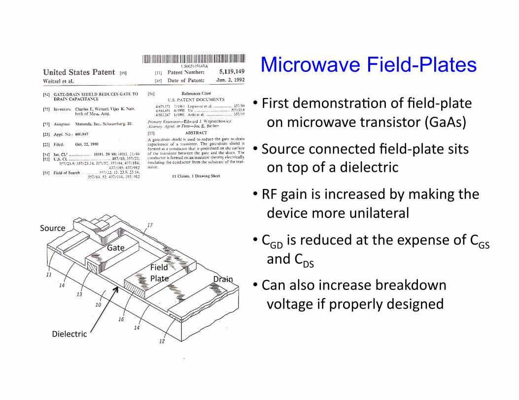
Microwave Field-Plates
• First demonstraKon of field‐plate on microwave transistor (GaAs)
• Source connected field‐plate sits on top of a dielectric
• RF gain is increased by making the device more unilateral
• CGD is reduced at the expense of CGS and CDS
• Can also increase breakdown voltage if properly designed
Source
Drain
Gate
Field Plate
Dielectric

Field‐Plate increases small signal gain approx. 3 dB

1.7 W/mm 1.5 GHz Vds = 35V

2003


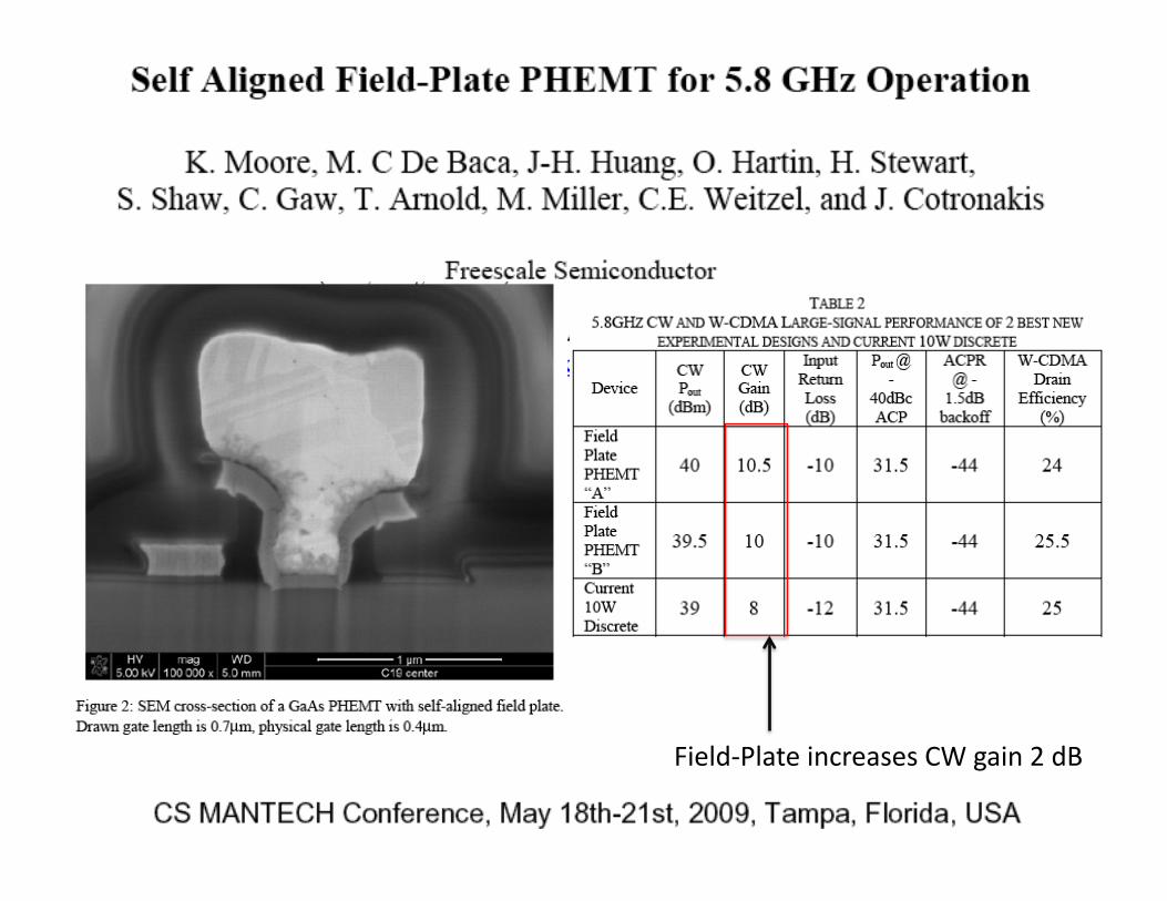
Field‐Plate increases CW gain 2 dB

AlGaN–GaN Field Effect Transistor
‐ the SiC MESFET “KILLER”

Basic AlGaN‐GaN HeterojuncKon FET
Substrate: Sapphire, SiC, or Silicon
+++++++++++++++++++++
Spontaneous and Piezoelectric PolarizaKon cause +++ charge in the AlGaN. The band structure forms a quantum well at the AlGaN‐GaN interface. Electrons fill the quantum well to a very high density > 1E7 cm‐2. There is no intenKonal doping.

Small Signal GaN HFET reported at SiC Conference in Kyoto, Japan


12.6 mm AlGaN/GaN HFET 48 V 2.14 GHz 74 W 5.9 W/mm No Field Plate IMS 2006


AlGaN/GaN HFET 30 V 15 GHz 60 W ~ 3 W/mm IMS 2010

Wide Bandgap Summary • Material properKes:
‐ high operaKng voltages ‐ high thermal conducKvity (SiC substrate)
• SiC MESFET first wide bandgap microwave power transistor
• Field Plates: ‐ increased RF gain ‐ even higher operaKng voltages
• AlGaN/GaN heterojuncKon achieves current density > 1 x 10¹³ A/cm2 (SiC MESFET “killer”)
• Heavily supported for US defense applicaKons, but is there a “killer” commercial applicaKon??