Embed Size (px)
Citation preview
Wide VIN 1A Synchronous Buck Regulator ISL85410The ISL85410 is a 1A synchronous buck regulator with an input range of 3V to 36V. It provides an easy to use, high efficiency low BOM count solution for a variety of applications.
The ISL85410 integrates both high-side and low-side NMOS FETs and features a PFM mode for improved efficiency at light loads. This feature can be disabled if a forced PWM mode is desired. The part switches at a default frequency of 500kHz but may also be programmed using an external resistor from 300kHz to 2MHz. The ISL85410 has the ability to utilize internal or external compensation. By integrating both NMOS devices and providing internal configuration options, minimal external components are required, reducing BOM count and complexity of design.
With the wide VIN range and reduced BOM, the part provides an easy to implement design solution for a variety of applications while giving superior performance. It will provide a very robust design for high voltage industrial applications as well as an efficient solution for battery powered applications.
The part is available in a small Pb-free 4mmx3mm DFN plastic package with a full-range industrial temperature of -40°C to +125°C.
Related Literature• AN1905, “ISL85410EVAL1Z, ISL85418EVAL1Z Wide VIN 1A,
800mA Synchronous Buck Regulator”
• AN1908, “ISL85410DEMO1Z, ISL85418DEMO1Z Wide VIN 1A, 800mA Synchronous Buck Regulator”
Features• Wide input voltage range 3V to 36V
• Synchronous operation for high efficiency
• No compensation required
• Integrated high-side and low-side NMOS devices
• Selectable PFM or forced PWM mode at light loads
• Internal fixed (500kHz) or adjustable switching frequency 300kHz to 2MHz
• Continuous output current up to 1A
• Internal or external soft-start
• Minimal external components required
• Power-good and enable functions available
Applications• Industrial control
• Medical devices
• Portable instrumentation
• Distributed power supplies
• Cloud infrastructure
FIGURE 1. TYPICAL APPLICATION FIGURE 2. EFFICIENCY vs LOAD, PFM, VOUT = 3.3V
GNDCBOOT
100nF
CFB
R3
R2
PHASE
SS
SYNC
BOOT
VIN
PGND
FS
COMP
FB
VCC
PG
EN
CVCC
1µF
CVIN
10µF
L1
22µH
1
2
3
4
5
6
9
10
11
12
INTERNAL DEFAULT PARAMETER SELECTION
COUT
10µF
VOUT
50
55
60
65
70
75
80
85
90
95
100VIN = 5V
VIN = 15V
VIN = 24V
VIN = 12V
VIN = 33V
OUTPUT LOAD (A)
EF
FIC
IEN
CY
(%
)
0 0.1 0.2 0.3 0.4 0.5 0.6 0.7 0.8 0.9 1.0
1 CAUTION: These devices are sensitive to electrostatic discharge; follow proper IC Handling Procedures.1-888-INTERSIL or 1-888-468-3774 | Copyright Intersil Americas LLC 2013, 2014. All Rights Reserved
Intersil (and design) is a trademark owned by Intersil Corporation or one of its subsidiaries.All other trademarks mentioned are the property of their respective owners.
July 24, 2014FN8375.5
ISL85410
Table of ContentsPin Configuration. . . . . . . . . . . . . . . . . . . . . . . . . . . . . . . . . . . . . . . . . . . . . . . . . . . . . . . . . . . . . . . . . . . . . . . . . . . . . . . . . . . . . . . . . . . . 3
Pin Descriptions. . . . . . . . . . . . . . . . . . . . . . . . . . . . . . . . . . . . . . . . . . . . . . . . . . . . . . . . . . . . . . . . . . . . . . . . . . . . . . . . . . . . . . . . . . . . . 3
Typical Application Schematics. . . . . . . . . . . . . . . . . . . . . . . . . . . . . . . . . . . . . . . . . . . . . . . . . . . . . . . . . . . . . . . . . . . . . . . . . . . . . . . . 4
Functional Block Diagram . . . . . . . . . . . . . . . . . . . . . . . . . . . . . . . . . . . . . . . . . . . . . . . . . . . . . . . . . . . . . . . . . . . . . . . . . . . . . . . . . . . . 5
Ordering Information . . . . . . . . . . . . . . . . . . . . . . . . . . . . . . . . . . . . . . . . . . . . . . . . . . . . . . . . . . . . . . . . . . . . . . . . . . . . . . . . . . . . . . . . 5
Absolute Maximum Ratings . . . . . . . . . . . . . . . . . . . . . . . . . . . . . . . . . . . . . . . . . . . . . . . . . . . . . . . . . . . . . . . . . . . . . . . . . . . . . . . . . . . 6
Thermal Information . . . . . . . . . . . . . . . . . . . . . . . . . . . . . . . . . . . . . . . . . . . . . . . . . . . . . . . . . . . . . . . . . . . . . . . . . . . . . . . . . . . . . . . . . 6
Recommended Operating Conditions . . . . . . . . . . . . . . . . . . . . . . . . . . . . . . . . . . . . . . . . . . . . . . . . . . . . . . . . . . . . . . . . . . . . . . . . . . 6
Electrical Specifications . . . . . . . . . . . . . . . . . . . . . . . . . . . . . . . . . . . . . . . . . . . . . . . . . . . . . . . . . . . . . . . . . . . . . . . . . . . . . . . . . . . . . 6
Efficiency Curves . . . . . . . . . . . . . . . . . . . . . . . . . . . . . . . . . . . . . . . . . . . . . . . . . . . . . . . . . . . . . . . . . . . . . . . . . . . . . . . . . . . . . . . . . . . . 8
Measurements . . . . . . . . . . . . . . . . . . . . . . . . . . . . . . . . . . . . . . . . . . . . . . . . . . . . . . . . . . . . . . . . . . . . . . . . . . . . . . . . . . . . . . . . . . . . . 10
Detailed Description . . . . . . . . . . . . . . . . . . . . . . . . . . . . . . . . . . . . . . . . . . . . . . . . . . . . . . . . . . . . . . . . . . . . . . . . . . . . . . . . . . . . . . . . 14Power-On Reset . . . . . . . . . . . . . . . . . . . . . . . . . . . . . . . . . . . . . . . . . . . . . . . . . . . . . . . . . . . . . . . . . . . . . . . . . . . . . . . . . . . . . . . . . . . . . . . . . 14Soft-Start. . . . . . . . . . . . . . . . . . . . . . . . . . . . . . . . . . . . . . . . . . . . . . . . . . . . . . . . . . . . . . . . . . . . . . . . . . . . . . . . . . . . . . . . . . . . . . . . . . . . . . . 14Power-Good . . . . . . . . . . . . . . . . . . . . . . . . . . . . . . . . . . . . . . . . . . . . . . . . . . . . . . . . . . . . . . . . . . . . . . . . . . . . . . . . . . . . . . . . . . . . . . . . . . . . 14PWM Control Scheme . . . . . . . . . . . . . . . . . . . . . . . . . . . . . . . . . . . . . . . . . . . . . . . . . . . . . . . . . . . . . . . . . . . . . . . . . . . . . . . . . . . . . . . . . . . . 14Light Load Operation. . . . . . . . . . . . . . . . . . . . . . . . . . . . . . . . . . . . . . . . . . . . . . . . . . . . . . . . . . . . . . . . . . . . . . . . . . . . . . . . . . . . . . . . . . . . . 15Output Voltage Selection . . . . . . . . . . . . . . . . . . . . . . . . . . . . . . . . . . . . . . . . . . . . . . . . . . . . . . . . . . . . . . . . . . . . . . . . . . . . . . . . . . . . . . . . . 15
Protection Features. . . . . . . . . . . . . . . . . . . . . . . . . . . . . . . . . . . . . . . . . . . . . . . . . . . . . . . . . . . . . . . . . . . . . . . . . . . . . . . . . . . . . . . . . 15Overcurrent Protection . . . . . . . . . . . . . . . . . . . . . . . . . . . . . . . . . . . . . . . . . . . . . . . . . . . . . . . . . . . . . . . . . . . . . . . . . . . . . . . . . . . . . . . . . . . 15Negative Current Limit . . . . . . . . . . . . . . . . . . . . . . . . . . . . . . . . . . . . . . . . . . . . . . . . . . . . . . . . . . . . . . . . . . . . . . . . . . . . . . . . . . . . . . . . . . . 16Over-Temperature Protection. . . . . . . . . . . . . . . . . . . . . . . . . . . . . . . . . . . . . . . . . . . . . . . . . . . . . . . . . . . . . . . . . . . . . . . . . . . . . . . . . . . . . . 16Boot Undervoltage Protection . . . . . . . . . . . . . . . . . . . . . . . . . . . . . . . . . . . . . . . . . . . . . . . . . . . . . . . . . . . . . . . . . . . . . . . . . . . . . . . . . . . . . 16
Application Guidelines . . . . . . . . . . . . . . . . . . . . . . . . . . . . . . . . . . . . . . . . . . . . . . . . . . . . . . . . . . . . . . . . . . . . . . . . . . . . . . . . . . . . . . 16Simplifying the Design . . . . . . . . . . . . . . . . . . . . . . . . . . . . . . . . . . . . . . . . . . . . . . . . . . . . . . . . . . . . . . . . . . . . . . . . . . . . . . . . . . . . . . . . . . . 16Operating Frequency . . . . . . . . . . . . . . . . . . . . . . . . . . . . . . . . . . . . . . . . . . . . . . . . . . . . . . . . . . . . . . . . . . . . . . . . . . . . . . . . . . . . . . . . . . . . . 16Synchronization Control . . . . . . . . . . . . . . . . . . . . . . . . . . . . . . . . . . . . . . . . . . . . . . . . . . . . . . . . . . . . . . . . . . . . . . . . . . . . . . . . . . . . . . . . . . 16Output Inductor Selection. . . . . . . . . . . . . . . . . . . . . . . . . . . . . . . . . . . . . . . . . . . . . . . . . . . . . . . . . . . . . . . . . . . . . . . . . . . . . . . . . . . . . . . . . 16Buck Regulator Output Capacitor Selection. . . . . . . . . . . . . . . . . . . . . . . . . . . . . . . . . . . . . . . . . . . . . . . . . . . . . . . . . . . . . . . . . . . . . . . . . . 17Loop Compensation Design . . . . . . . . . . . . . . . . . . . . . . . . . . . . . . . . . . . . . . . . . . . . . . . . . . . . . . . . . . . . . . . . . . . . . . . . . . . . . . . . . . . . . . . 17Layout Considerations. . . . . . . . . . . . . . . . . . . . . . . . . . . . . . . . . . . . . . . . . . . . . . . . . . . . . . . . . . . . . . . . . . . . . . . . . . . . . . . . . . . . . . . . . . . . 19
Revision History. . . . . . . . . . . . . . . . . . . . . . . . . . . . . . . . . . . . . . . . . . . . . . . . . . . . . . . . . . . . . . . . . . . . . . . . . . . . . . . . . . . . . . . . . . . . 20
About Intersil . . . . . . . . . . . . . . . . . . . . . . . . . . . . . . . . . . . . . . . . . . . . . . . . . . . . . . . . . . . . . . . . . . . . . . . . . . . . . . . . . . . . . . . . . . . . . . 20
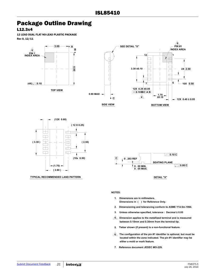
Package Outline Drawing . . . . . . . . . . . . . . . . . . . . . . . . . . . . . . . . . . . . . . . . . . . . . . . . . . . . . . . . . . . . . . . . . . . . . . . . . . . . . . . . . . . . 21
2 FN8375.5July 24, 2014
Submit Document Feedback
ISL85410
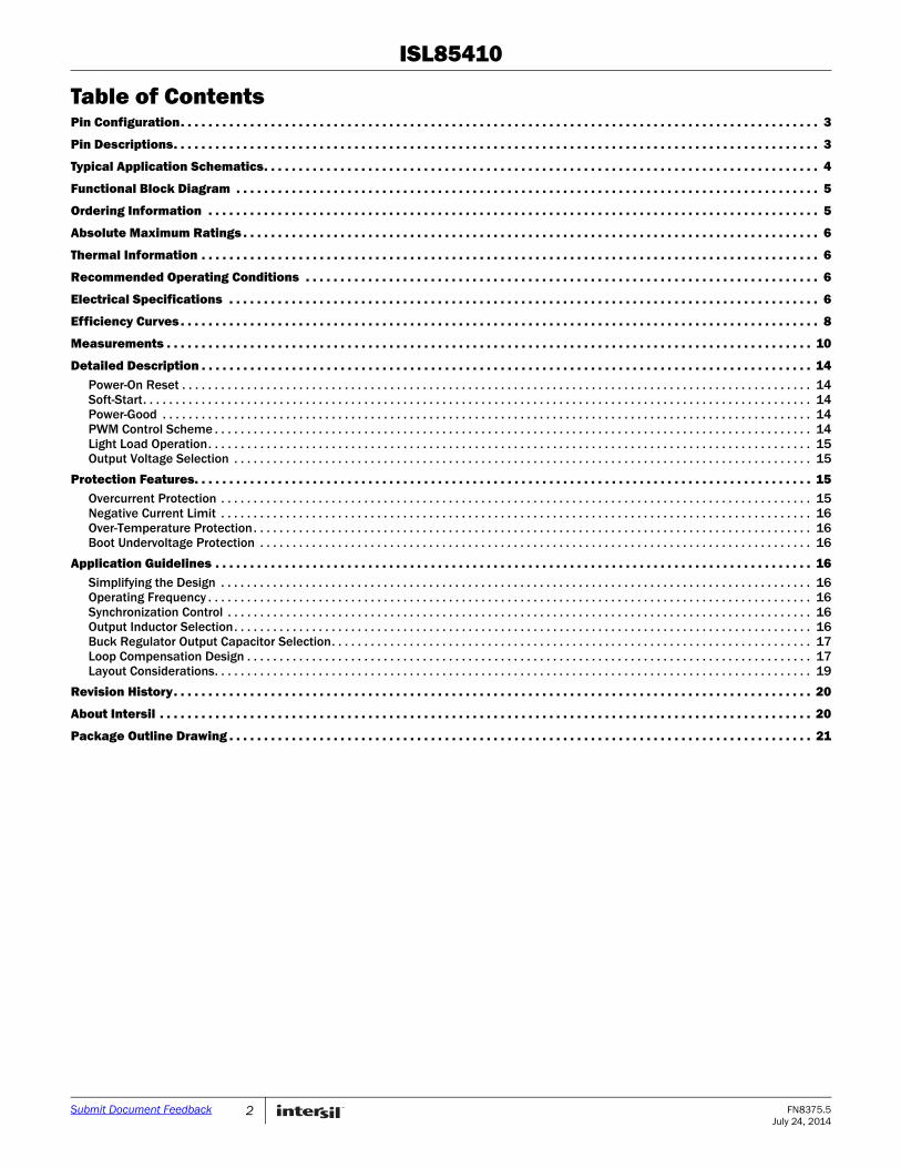
Pin ConfigurationISL85410
(12 LD 3x4 DFN)TOP VIEW
VCC
EN
VIN
FB
PHASE
BOOT
COMP
1
2
3
4
5
12
11
10
9
8 PG
SS FS
PGND 6
GND
7
SYNC
Pin DescriptionsPIN NUMBER SYMBOL PIN DESCRIPTION
1 SS The SS pin controls the soft-start ramp time of the output. A single capacitor from the SS pin to ground determines the output ramp rate. See “Soft-Start” on page 14 for soft-start details. If the SS pin is tied to VCC, an internal soft-start of 2ms will be used.
2 SYNC Synchronization and light load operational mode selection input. Connect to logic high or VCC for PWM mode. Connect to logic low or ground for PFM mode. Logic ground enables the IC to automatically choose PFM or PWM operation. Connect to an external clock source for synchronization with positive edge trigger. Sync source must be higher than the programmed IC frequency. There is an internal 5MΩ pull-down resistor to prevent an undefined logic state if SYNC is left floating.
3 BOOT Floating bootstrap supply pin for the power MOSFET gate driver. The bootstrap capacitor provides the necessary charge to turn on the internal N-Channel MOSFET. Connect an external 100nF capacitor from this pin to PHASE.
4 VIN The input supply for the power stage of the regulator and the source for the internal linear bias regulator. Place a minimum of 4.7µF ceramic capacitance from VIN to GND and close to the IC for decoupling.
5 PHASE Switch node output. It connects the switching FETs with the external output inductor.
6 PGND Power ground connection. Connect directly to the system GND plane.
7 EN Regulator enable input. The regulator and bias LDO are held off when the pin is pulled to ground. When the voltage on this pin rises above 1V, the chip is enabled. Connect this pin to VIN for automatic start-up. Do not connect EN pin to VCC since the LDO is controlled by EN voltage.
8 PG Open-drain power-good output that is pulled to ground when the output voltage is below regulation limits or during the soft-start interval. There is an internal 5MΩ internal pull-up resistor.
9 VCC Output of the internal 5V linear bias regulator. Decouple to PGND with a 1µF ceramic capacitor at the pin.
10 FB Feedback pin for the regulator. FB is the inverting input to the voltage loop error amplifier. COMP is the output of the error amplifier. The output voltage is set by an external resistor divider connected to FB. In addition, the PWM regulator’s power-good and UVLO circuits use FB to monitor the regulator output voltage.
11 COMP COMP is the output of the error amplifier. When it is tied to VCC, internal compensation is used. When only an RC network is connected from COMP to GND, external compensation is used. See “Loop Compensation Design” on page 17 for more details.
12 FS Frequency selection pin. Tie to VCC for 500kHz switching frequency. Connect a resistor to GND for adjustable frequency from 300kHz to 2MHz.
EPAD GND Signal ground connections. Connect to application board GND plane with at least 5 vias. All voltage levels are measured with respect to this pin. The EPAD MUST NOT float.
3 FN8375.5July 24, 2014
Submit Document Feedback

ISL85410
Typical Application Schematics
FIGURE 3. INTERNAL DEFAULT PARAMETER SELECTION
FIGURE 4. USER PROGRAMMABLE PARAMETER SELECTION
GNDCBOOT
100nF
CFB
R3
R2
PHASE
SS
SYNC
BOOT
VIN
PGND
FS
COMP
FB
VCC
PG
EN
CVCC
1µF
CVIN
10µF
L1
22µH
1
2
3
4
5
6
9
10
11
12
COUT
10µF
VOUT
GNDCBOOT
100nF
CFB
R3
R2
CSS
CCOMP
RCOMP
RFS
PHASE
SS
SYNC
BOOT
VIN
PGND
FS
COMP
FB
VCC
PG
EN
CVIN
10µFCVCC
1µF
L1
22µHCOUT
10µF
1
2
3
4
5
6
9
10
11
12
VOUT
TABLE 1. EXTERNAL COMPONENT SELECTION
VOUT(V)
L1(µH)
COUT(µF)
R2(kΩ)
R3(kΩ)
CFB(pF)
RFS(kΩ)
RCOMP(kΩ)
CCOMP(pF)
12 22 2 x 22 90.9 4.75 22 115 150 470
5 22 47 + 22 90.9 12.4 27 DNP (Note 1) 100 470
3.3 22 47 + 22 90.9 20 27 DNP (Note 1) 100 470
2.5 22 47 + 22 90.9 28.7 27 DNP (Note 1) 100 470
1.8 12 47 + 22 90.9 45.5 27 DNP (Note 1) 70 470
NOTE:1. Connect FS to VCC.
4 FN8375.5July 24, 2014
Submit Document Feedback
ISL85410
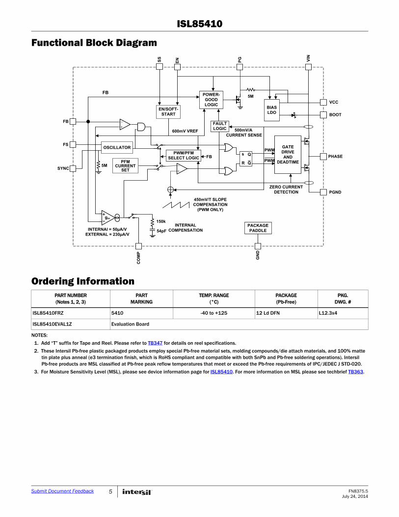
Functional Block Diagram
GATE DRIVE AND
DEADTIME
BIAS LDO
OSCILLATOR
PFM CURRENT
SET
FAULTLOGIC
450mV/T SLOPE COMPENSATION
(PWM ONLY)
500mV/A CURRENT SENSE
PWM/PFM SELECT LOGIC
EN/SOFT- START
ZERO CURRENT DETECTION
PWM
PWM
600mV VREF
gm150k
54pFINTERNAL
COMPENSATION
s
R
Q
Q
POWER- GOOD LOGIC
FB
INTERNAl = 50µA/VEXTERNAL = 230µA/V
5M
5M
PGND
PHASE
BOOT
VCC
VIN
EN
FB
FS
SYNC
CO
MP
PG
GN
D
PACKAGE PADDLE
SS
FB
Ordering InformationPART NUMBER(Notes 1, 2, 3)
PART MARKING
TEMP. RANGE (°C)
PACKAGE(Pb-Free)
PKG.DWG. #
ISL85410FRZ 5410 -40 to +125 12 Ld DFN L12.3x4
ISL85410EVAL1Z Evaluation Board
NOTES:
1. Add “T” suffix for Tape and Reel. Please refer to TB347 for details on reel specifications.
2. These Intersil Pb-free plastic packaged products employ special Pb-free material sets, molding compounds/die attach materials, and 100% matte tin plate plus anneal (e3 termination finish, which is RoHS compliant and compatible with both SnPb and Pb-free soldering operations). Intersil Pb-free products are MSL classified at Pb-free peak reflow temperatures that meet or exceed the Pb-free requirements of IPC/JEDEC J STD-020.
3. For Moisture Sensitivity Level (MSL), please see device information page for ISL85410. For more information on MSL please see techbrief TB363.
5 FN8375.5July 24, 2014
Submit Document Feedback
ISL85410
Absolute Maximum Ratings Thermal InformationVIN to GND. . . . . . . . . . . . . . . . . . . . . . . . . . . . . . . . . . . . . . . . . -0.3V to +42VPHASE to GND. . . . . . . . . . . . . . . . . . . . . . . . . . . . . . . -0.3V to VIN+0.3V (DC)PHASE to GND. . . . . . . . . . . . . . . . . . . . . . . . . . . . . . . . . . . -2V to 43V (20ns)EN to GND . . . . . . . . . . . . . . . . . . . . . . . . . . . . . . . . . . . . . . . . . -0.3V to +42VBOOT to PHASE. . . . . . . . . . . . . . . . . . . . . . . . . . . . . . . . . . . . . -0.3V to +5.5VCOMP, FS, PG, SYNC, SS, VCC to GND . . . . . . . . . . . . . . . . . . -0.3V to +5.9VFB to GND . . . . . . . . . . . . . . . . . . . . . . . . . . . . . . . . . . . . . . . . -0.3V to +2.95VESD Rating
Human Body Model (Tested per JESD22-A114) . . . . . . . . . . . . . . . . . 2kV Charged Device Model (Tested per JESD22-C101E). . . . . . . . . . . . .1.5kV Latch Up (Tested per JESD-78A; Class 2, Level A) . . . . . . . . . . . . 100mA
Thermal Resistance JA (°C/W) JC (°C/W)DFN Package (Notes 4, 5) . . . . . . . . . . . . . . 42 4.5
Maximum Junction Temperature (Plastic Package) . . . . . . . . . . . .+150°CMaximum Storage Temperature Range . . . . . . . . . . . . . .-65°C to +150°CAmbient Temperature Range . . . . . . . . . . . . . . . . . . . . . . .-40°C to +125°COperating Junction Temperature Range . . . . . . . . . . . . . .-40°C to +125°CPb-Free Reflow Profile . . . . . . . . . . . . . . . . . . . . . . . . . . . . . . . . . . see TB493
Recommended Operating ConditionsTemperature . . . . . . . . . . . . . . . . . . . . . . . . . . . . . . . . . . . . .-40°C to +125°CSupply Voltage . . . . . . . . . . . . . . . . . . . . . . . . . . . . . . . . . . . . . . . . . 3V to 36V
CAUTION: Do not operate at or near the maximum ratings listed for extended periods of time. Exposure to such conditions may adversely impact productreliability and result in failures not covered by warranty.
NOTES:
4. JA is measured in free air with the component mounted on a high effective thermal conductivity test board with “direct attach” features. See Tech Brief TB379 for details.
5. For JC, the “case temp” location is the center of the exposed metal pad on the package underside.
Electrical Specifications TA = -40°C to +125°C, VIN = 3V to 36V, unless otherwise noted. Typical values are at TA = +25°C. Boldface limits apply across the junction temperature range, -40°C to +125°C
PARAMETER SYMBOL TEST CONDITIONSMIN
(Note 8) TYPMAX
(Note 8) UNITS
SUPPLY VOLTAGE
VIN Voltage Range VIN 3 36 V
VIN Quiescent Supply Current IQ VFB = 0.7V, SYNC = 0V, fSW = VCC 80 µA
VIN Shutdown Supply Current ISD EN = 0V, VIN = 36V (Note 6) 2 4 µA
VCC Voltage VCC VIN = 6V, IOUT = 0 to 10mA 4.5 5.1 5.7 V
POWER-ON RESET
VCC POR Threshold Rising edge 2.75 2.95 V
Falling edge 2.35 2.6 V
OSCILLATOR
Nominal Switching Frequency fSW FS pin = VCC 430 500 570 kHz
Resistor from FS pin to GND = 340kΩ 240 300 360 kHz
Resistor from FS pin to GND = 32.4kΩ 2000 kHz
Minimum Off-Time tOFF VIN = 3V 150 ns
Minimum On-Time tON (Note 9) 90 ns
FS Voltage VFS RFS = 100k 0.39 0.4 0.41 V
Synchronization Frequency SYNC 300 2000 kHz
SYNC Pulse Width 100 ns
ERROR AMPLIFIER
Error Amplifier Transconductance Gain gm External compensation 165 230 295 µA/V
Internal compensation 50 µA/V
FB Leakage Current VFB = 0.6V 1 150 nA
Current Sense Amplifier Gain RT 0.46 0.5 0.54 V/A
FB Voltage TA = -40°C to +85°C 0.590 0.599 0.606 V
TA = -40°C to +125°C 0.590 0.599 0.607 V
6 FN8375.5July 24, 2014
Submit Document Feedback
ISL85410
POWER-GOOD
Lower PG Threshold - VFB Rising 90 94 %
Lower PG Threshold - VFB Falling 82.5 86 %
Upper PG Threshold - VFB Rising 116.5 120 %
Upper PG Threshold - VFB Falling 107 112 %
PG Propagation Delay Percentage of the soft-start time 10 %
PG Low Voltage ISINK = 3mA, EN = VCC, VFB = 0V 0.05 0.3 V
TRACKING AND SOFT-START
Soft-Start Charging Current ISS 4.2 5.5 6.5 µA
Internal Soft-Start Ramp Time EN/SS = VCC 1.5 2.4 3.4 ms
FAULT PROTECTION
Thermal Shutdown Temperature TSD Rising threshold 150 °C
THYS Hysteresis 20 °C
Current Limit Blanking Time tOCON 17 Clock pulses
Overcurrent and Auto Restart Period tOCOFF 8 SS cycle
Positive Peak Current Limit IPLIMIT (Note 7) 1.3 1.5 1.7 A
PFM Peak Current Limit IPK_PFM 0.34 0.4 0.5 A
Zero Cross Threshold 15 mA
Negative Current Limit INLIMIT (Note 7) -0.67 -0.6 -0.53 A
POWER MOSFET
High-side RHDS IPHASE = 100mA, VCC = 5V 250 350 mΩ
Low-side RLDS IPHASE = 100mA, VCC = 5V 90 130 mΩ
PHASE Leakage Current EN = PHASE = 0V 300 nA
PHASE Rise Time tRISE VIN = 36V 10 ns
EN/SYNC
Input Threshold Falling edge, logic low 0.4 1 V
Rising edge, logic high 1.2 1.4 V
EN Logic Input Leakage Current EN = 0V/36V -0.5 0.5 µA
SYNC Logic Input Leakage Current SYNC = 0V 10 100 nA
SYNC = 5V 1.0 1.55 µA
NOTES:
6. Test Condition: VIN = 36V, FB forced above regulation point (0.6V), no switching, and power MOSFET gate charging current not included.
7. Established by both current sense amplifier gain test and current sense amplifier output test at IL = 0A.
8. Parameters with MIN and/or MAX limits are 100% tested at +25°C, unless otherwise specified. Temperature limits established by characterization and are not production tested.
9. Minimum On-Time required to maintain loop stability.
Electrical Specifications TA = -40°C to +125°C, VIN = 3V to 36V, unless otherwise noted. Typical values are at TA = +25°C. Boldface limits apply across the junction temperature range, -40°C to +125°C (Continued)
PARAMETER SYMBOL TEST CONDITIONSMIN
(Note 8) TYPMAX
(Note 8) UNITS
7 FN8375.5July 24, 2014
Submit Document Feedback
ISL85410
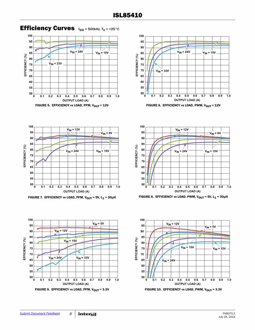
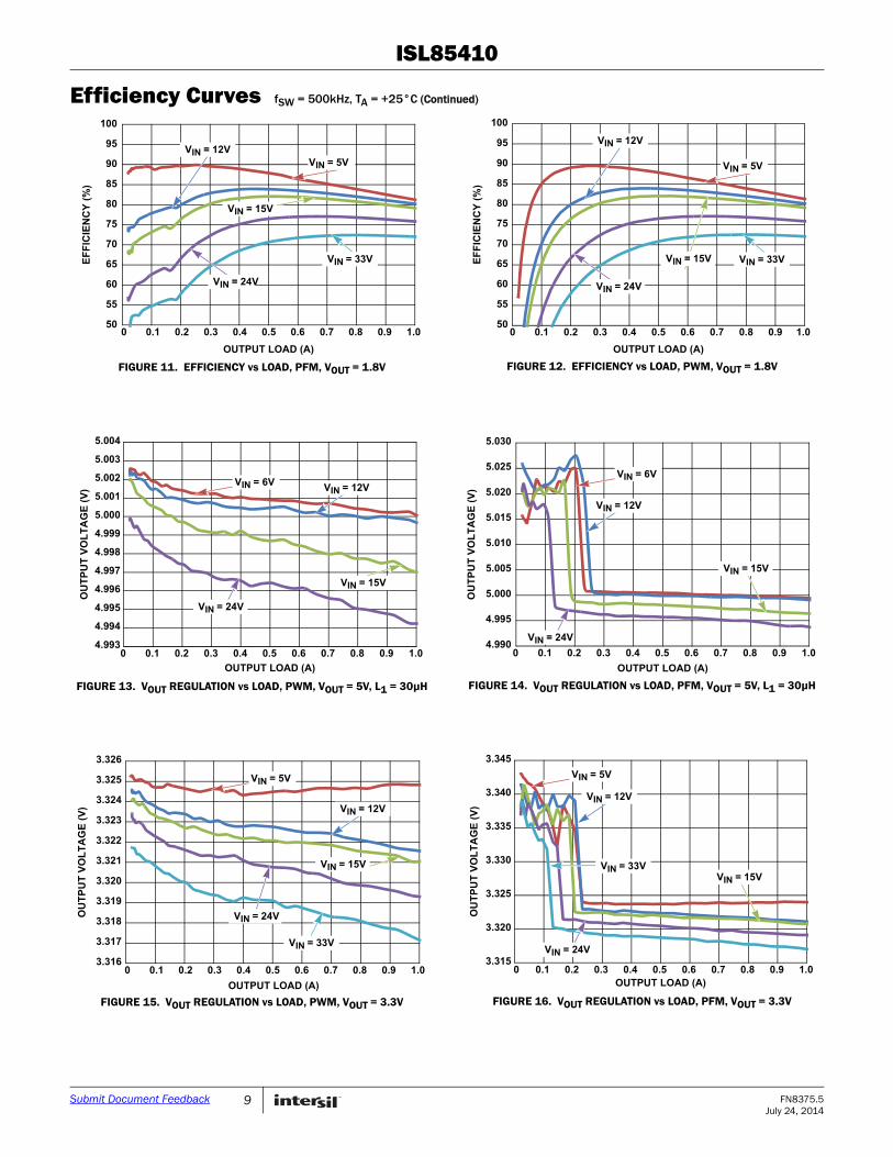
Efficiency Curves fSW = 500kHz, TA = +25°C
FIGURE 5. EFFICIENCY vs LOAD, PFM, VOUT = 12V FIGURE 6. EFFICIENCY vs LOAD, PWM, VOUT = 12V
FIGURE 7. EFFICIENCY vs LOAD, PFM, VOUT = 5V, L1 = 30µH FIGURE 8. EFFICIENCY vs LOAD, PWM, VOUT = 5V, L1 = 30µH
FIGURE 9. EFFICIENCY vs LOAD, PFM, VOUT = 3.3V FIGURE 10. EFFICIENCY vs LOAD, PWM, VOUT = 3.3V
50
55
60
65
70
75
80
85
90
95
100
0 0.1 0.2 0.3 0.4 0.5 0.6 0.7 0.8 0.9 1.0
VIN = 15V VIN = 24V
VIN = 33V
OUTPUT LOAD (A)
EF
FIC
IEN
CY
(%
)
50
55
60
65
70
75
80
85
90
95
100
0 0.1 0.2 0.3 0.4 0.5 0.6 0.7 0.8 0.9 1.0
VIN = 15V VIN = 24V
VIN = 33V
OUTPUT LOAD (A)
EF
FIC
IEN
CY
(%
)
50
55
60
65
70
75
80
85
90
95
100
0 0.1 0.2 0.3 0.4 0.5 0.6 0.7 0.8 0.9 1.0
OUTPUT LOAD (A)
EF
FIC
IEN
CY
(%
)
VIN = 6V
VIN = 15V VIN = 24V
VIN = 12V
50
55
60
65
70
75
80
85
90
95
100
0 0.1 0.2 0.3 0.4 0.5 0.6 0.7 0.8 0.9 1.0
OUTPUT LOAD (A)
EF
FIC
IEN
CY
(%
)VIN = 6V
VIN = 15V VIN = 24V
VIN = 12V
50
55
60
65
70
75
80
85
90
95
100VIN = 5V
VIN = 15V
VIN = 24V
VIN = 12V
VIN = 33V
OUTPUT LOAD (A)
EF
FIC
IEN
CY
(%
)
0 0.1 0.2 0.3 0.4 0.5 0.6 0.7 0.8 0.9 1.0 50
55
60
65
70
75
80
85
90
95
100
0 0.1 0.2 0.3 0.4 0.5 0.6 0.7 0.8 0.9 1.0
OUTPUT LOAD (A)
EF
FIC
IEN
CY
(%
)
VIN = 5V
VIN = 15V
VIN = 24V
VIN = 12V
VIN = 33V
8 FN8375.5July 24, 2014
Submit Document Feedback
ISL85410
FIGURE 11. EFFICIENCY vs LOAD, PFM, VOUT = 1.8V FIGURE 12. EFFICIENCY vs LOAD, PWM, VOUT = 1.8V
FIGURE 13. VOUT REGULATION vs LOAD, PWM, VOUT = 5V, L1 = 30µH FIGURE 14. VOUT REGULATION vs LOAD, PFM, VOUT = 5V, L1 = 30µH
FIGURE 15. VOUT REGULATION vs LOAD, PWM, VOUT = 3.3V FIGURE 16. VOUT REGULATION vs LOAD, PFM, VOUT = 3.3V
Efficiency Curves fSW = 500kHz, TA = +25°C (Continued)
50
55
60
65
70
75
80
85
90
95
100
0 0.1 0.2 0.3 0.4 0.5 0.6 0.7 0.8 0.9 1.0
VIN = 5V
VIN = 15V
VIN = 24V
VIN = 12V
VIN = 33V
OUTPUT LOAD (A)
EF
FIC
IEN
CY
(%
)
0 0.1 0.2 0.3 0.4 0.5 0.6 0.7 0.8 0.9 1.0 50
55
60
65
70
75
80
85
90
95
100
VIN = 5V
VIN = 15V
VIN = 24V
VIN = 12V
VIN = 33V
OUTPUT LOAD (A)
EF
FIC
IEN
CY
(%
)
4.993
4.994
4.995
4.996
4.997
4.998
4.999
5.000
5.001
5.002
5.003
5.004
0 0.1 0.2 0.3 0.4 0.5 0.6 0.7 0.8 0.9 1.0
OUTPUT LOAD (A)
OU
TP
UT
VO
LT
AG
E (
V)
VIN = 6V
VIN = 15V
VIN = 24V
VIN = 12V
4.990
4.995
5.000
5.005
5.010
5.015
5.020
5.025
5.030
0 0.1 0.2 0.3 0.4 0.5 0.6 0.7 0.8 0.9 1.0
OUTPUT LOAD (A)
OU
TP
UT
VO
LT
AG
E (
V)
VIN = 6V
VIN = 15V
VIN = 24V
VIN = 12V
3.316
3.317
3.318
3.319
3.320
3.321
3.322
3.323
3.324
3.325
3.326
0 0.1 0.2 0.3 0.4 0.5 0.6 0.7 0.8 0.9 1.0
OUTPUT LOAD (A)
OU
TP
UT
VO
LT
AG
E (
V)
VIN = 5V
VIN = 15V
VIN = 12V
VIN = 33V
VIN = 24V
3.315
3.320
3.325
3.330
3.335
3.340
3.345
0 0.1 0.2 0.3 0.4 0.5 0.6 0.7 0.8 0.9 1.0 OUTPUT LOAD (A)
OU
TP
UT
VO
LT
AG
E (
V)
VIN = 5V
VIN = 15V
VIN = 24V
VIN = 12V
VIN = 33V
9 FN8375.5July 24, 2014
Submit Document Feedback
ISL85410
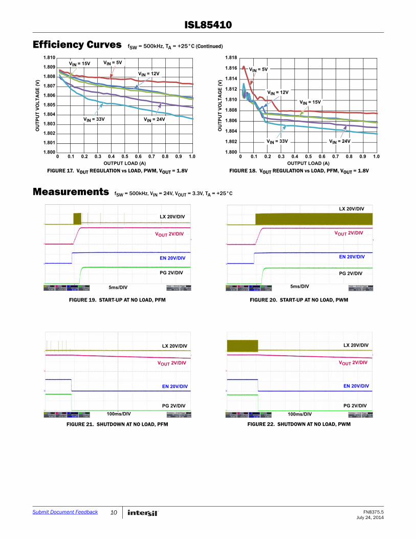
FIGURE 17. VOUT REGULATION vs LOAD, PWM, VOUT = 1.8V FIGURE 18. VOUT REGULATION vs LOAD, PFM, VOUT = 1.8V
Efficiency Curves fSW = 500kHz, TA = +25°C (Continued)
1.800
1.801
1.802
1.803
1.804
1.805
1.806
1.807
1.808
1.809
1.810
0 0.1 0.2 0.3 0.4 0.5 0.6 0.7 0.8 0.9 1.0
VIN = 5V VIN = 15V
VIN = 24V VIN = 33V
VIN = 12V
OUTPUT LOAD (A)
OU
TP
UT
VO
LT
AG
E (
V)
1.800
1.802
1.804
1.806
1.808
1.810
1.812
1.814
1.816
1.818
0 0.1 0.2 0.3 0.4 0.5 0.6 0.7 0.8 0.9 1.0
OUTPUT LOAD (A)
OU
TP
UT
VO
LT
AG
E (
V)
VIN = 5V
VIN = 15V
VIN = 24V VIN = 33V
VIN = 12V
Measurements fSW = 500kHz, VIN = 24V, VOUT = 3.3V, TA = +25°C
FIGURE 19. START-UP AT NO LOAD, PFM FIGURE 20. START-UP AT NO LOAD, PWM
FIGURE 21. SHUTDOWN AT NO LOAD, PFM FIGURE 22. SHUTDOWN AT NO LOAD, PWM
LX 20V/DIV
VOUT 2V/DIV
EN 20V/DIV
PG 2V/DIV
5ms/DIV
LX 20V/DIV
VOUT 2V/DIV
EN 20V/DIV
PG 2V/DIV
5ms/DIV
LX 20V/DIV
VOUT 2V/DIV
EN 20V/DIV
PG 2V/DIV
100ms/DIV
LX 20V/DIV
VOUT 2V/DIV
EN 20V/DIV
PG 2V/DIV
100ms/DIV
10 FN8375.5July 24, 2014
Submit Document Feedback

ISL85410
FIGURE 23. START-UP AT 1A, PWM FIGURE 24. SHUTDOWN AT 1A, PWM
FIGURE 25. START-UP AT 1A, PFM FIGURE 26. SHUTDOWN AT 1A, PFM
FIGURE 27. JITTER AT NO LOAD, PWM FIGURE 28. JITTER AT 1A LOAD, PWM
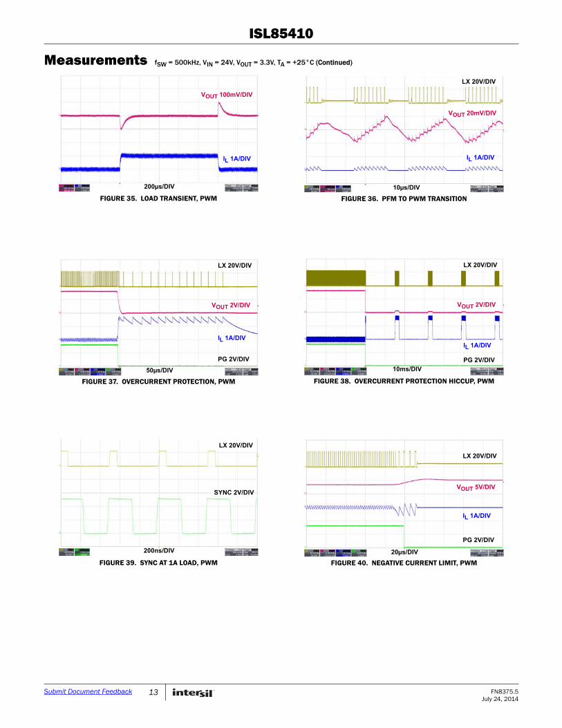
Measurements fSW = 500kHz, VIN = 24V, VOUT = 3.3V, TA = +25°C (Continued)
LX 20V/DIV
VOUT 2V/DIV
IL 500mA/DIV
PG 2V/DIV
5ms/DIV
LX 20V/DIV
VOUT 2V/DIV
IL 500mA/DIV
PG 2V/DIV
200µs/DIV
LX 20V/DIV
VOUT 2V/DIV
IL 500mA/DIV
PG 2V/DIV
5ms/DIV
LX 20V/DIV
VOUT 2V/DIV
IL 500mA/DIV
PG 2V/DIV
200µs/DIV
LX 5V/DIV
5ns/DIV
LX 5V/DIV
5ns/DIV
11 FN8375.5July 24, 2014
Submit Document Feedback

ISL85410
FIGURE 29. STEADY STATE AT NO LOAD, PFM FIGURE 30. STEADY STATE AT NO LOAD, PWM
FIGURE 31. STEADY STATE AT 1A, PWM FIGURE 32. LIGHT LOAD OPERATION AT 20mA, PFM
FIGURE 33. LIGHT LOAD OPERATION AT 20mA, PWM FIGURE 34. LOAD TRANSIENT, PFM
Measurements fSW = 500kHz, VIN = 24V, VOUT = 3.3V, TA = +25°C (Continued)
LX 20V/DIV
VOUT 20mV/DIV
IL 20mA/DIV
10ms/DIV
LX 20V/DIV
VOUT 20mV/DIV
IL 20mA/DIV
1µs/DIV
LX 20V/DIV
IL 1A/DIV
1µs/DIV
VOUT 20mV/DIV
LX 20V/DIV
IL 200mA/DIV
10µs/DIV
VOUT 50mV/DIV
LX 20V/DIV
IL 200mA/DIV
1µs/DIV
VOUT 10mV/DIV
IL 1A/DIV
200µs/DIV
VOUT 100mV/DIV
12 FN8375.5July 24, 2014
Submit Document Feedback
ISL85410
FIGURE 35. LOAD TRANSIENT, PWM FIGURE 36. PFM TO PWM TRANSITION
FIGURE 37. OVERCURRENT PROTECTION, PWM FIGURE 38. OVERCURRENT PROTECTION HICCUP, PWM
FIGURE 39. SYNC AT 1A LOAD, PWM FIGURE 40. NEGATIVE CURRENT LIMIT, PWM
Measurements fSW = 500kHz, VIN = 24V, VOUT = 3.3V, TA = +25°C (Continued)
IL 1A/DIV
200µs/DIV
VOUT 100mV/DIV
LX 20V/DIV
IL 1A/DIV
VOUT 20mV/DIV
10µs/DIV
LX 20V/DIV
VOUT 2V/DIV
IL 1A/DIV
PG 2V/DIV
50µs/DIV
LX 20V/DIV
VOUT 2V/DIV
IL 1A/DIV
PG 2V/DIV
10ms/DIV
LX 20V/DIV
SYNC 2V/DIV
200ns/DIV
LX 20V/DIV
VOUT 5V/DIV
IL 1A/DIV
PG 2V/DIV
20µs/DIV
13 FN8375.5July 24, 2014
Submit Document Feedback
ISL85410
Detailed DescriptionThe ISL85410 combines a synchronous buck PWM controller with integrated power switches. The buck controller drives internal high-side and low-side N-channel MOSFETs to deliver load current up to 1A. The buck regulator can operate from an unregulated DC source, such as a battery, with a voltage ranging from +3V to +36V. An internal LDO provides bias to the low voltage portions of the IC.
Peak current mode control is utilized to simplify feedback loop compensation and reject input voltage variation. User selectable internal feedback loop compensation further simplifies design. The ISL85410 switches at a default 500kHz.
The buck regulator is equipped with an internal current sensing circuit and the peak current limit threshold is typically set at 1.5A.
Power-On ResetThe ISL85410 automatically initializes upon receipt of the input power supply and continually monitors the EN pin state. If EN is held below its logic rising threshold, the IC is held in shutdown and consumes typically 2µA from the VIN supply. If EN exceeds its logic rising threshold, the regulator will enable the bias LDO and begin to monitor the VCC pin voltage. When the VCC pin voltage clears its rising POR threshold, the controller will initialize the switching regulator circuits. If VCC never clears the rising POR threshold, the controller will not allow the switching regulator to operate. If VCC falls below its falling POR threshold while the switching regulator is operating, the switching regulator will be shut down until VCC returns.
Soft-StartTo avoid large in-rush current, VOUT is slowly increased at start-up to its final regulated value. Soft-start time is determined by the SS pin connection. If SS is pulled to VCC, an internal 2ms timer is selected for soft-start. For other soft-start times, simply connect a capacitor from SS to GND. In this case, a 5.5µA current pulls up the SS voltage and the FB pin will follow this ramp until it reaches the 600mV reference level. Soft-start time for this case is described by Equation 1:
Power-GoodPG is the open-drain output of a window comparator that continuously monitors the buck regulator output voltage via the FB pin. PG is actively held low when EN is low and during the buck regulator soft-start period. After the soft-start period completes, PG becomes high impedance provided the FB pin is within the range specified in the “Electrical Specifications” on page 7. Should FB exit the specified window, PG will be pulled low until FB returns. Over-temperature faults also force PG low until the fault condition is cleared by an attempt to soft-start. There is an internal 5MΩ internal pull-up resistor.
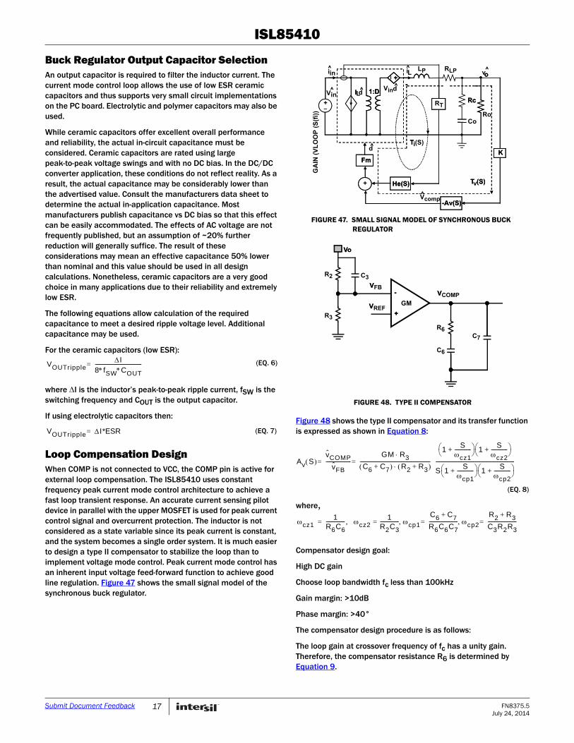
PWM Control SchemeThe ISL85410 employs peak current-mode pulse-width modulation (PWM) control for fast transient response and pulse-by-pulse current limiting, as shown in the “Functional Block Diagram” on page 5. The current loop consists of the current sensing circuit, slope compensation ramp, PWM comparator, oscillator and latch. Current sense trans-resistance is typically 500mV/A and slope compensation rate, Se, is typically 450mV/T where T is the switching cycle period. The control reference for the current loop comes from the error amplifier’s output (VCOMP).
A PWM cycle begins when a clock pulse sets the PWM latch and the upper FET is turned on. Current begins to ramp up in the upper FET and inductor. This current is sensed (VCSA), converted to a voltage and summed with the slope compensation signal. This combined signal is compared to VCOMP and when the signal is equal to VCOMP, the latch is reset. Upon latch reset, the upper FET is turned off and the lower FET turned on allowing current to ramp down in the inductor. The lower FET will remain on until the clock initiates another PWM cycle. Figure 44 shows the typical operating waveforms during the PWM operation. The dotted lines illustrate the sum of the current sense and slope compensation signal.
Output voltage is regulated as the error amplifier varies VCOMP and thus output inductor current. The error amplifier is a transconductance type and its output (COMP) is terminated with a series RC network to GND. This termination is internal (150k/54pF) if the COMP pin is tied to VCC. Additionally, the transconductance for COMP = VCC is 50µA/V vs 230µA/V for external RC connection. Its noninverting input is internally connected to a 600mV reference voltage and its inverting input is connected to the output voltage via the FB pin and its associated divider network.
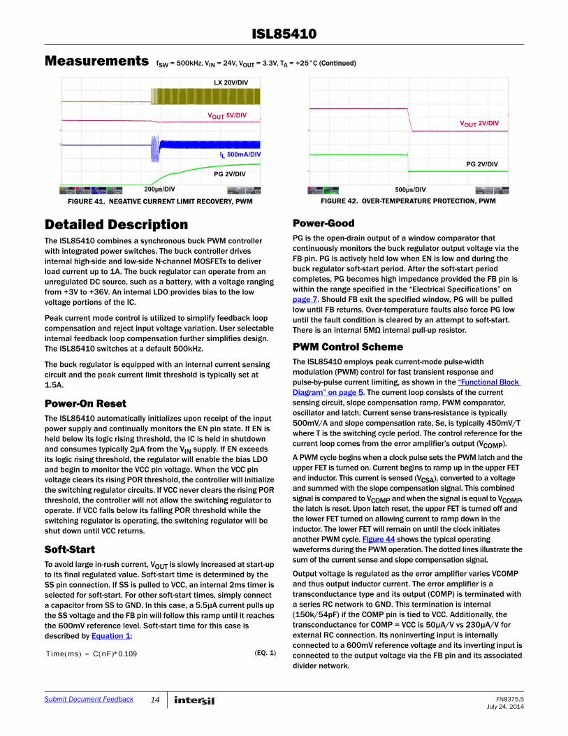
FIGURE 41. NEGATIVE CURRENT LIMIT RECOVERY, PWM FIGURE 42. OVER-TEMPERATURE PROTECTION, PWM
Measurements fSW = 500kHz, VIN = 24V, VOUT = 3.3V, TA = +25°C (Continued)
LX 20V/DIV
VOUT 5V/DIV
IL 500mA/DIV
PG 2V/DIV
200µs/DIV
VOUT 2V/DIV
PG 2V/DIV
500µs/DIV
Time ms C nF 0.109= (EQ. 1)
14 FN8375.5July 24, 2014
Submit Document Feedback
ISL85410
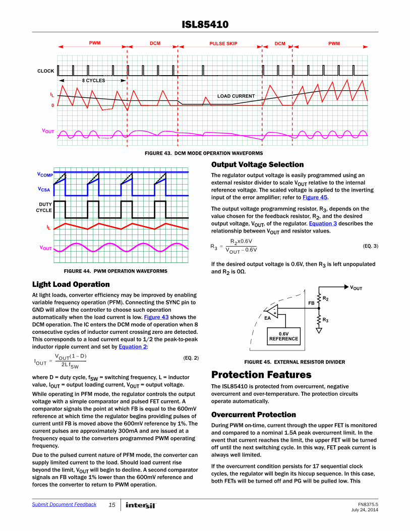
Light Load OperationAt light loads, converter efficiency may be improved by enabling variable frequency operation (PFM). Connecting the SYNC pin to GND will allow the controller to choose such operation automatically when the load current is low. Figure 43 shows the DCM operation. The IC enters the DCM mode of operation when 8 consecutive cycles of inductor current crossing zero are detected. This corresponds to a load current equal to 1/2 the peak-to-peak inductor ripple current and set by Equation 2:
where D = duty cycle, fSW = switching frequency, L = inductor value, IOUT = output loading current, VOUT = output voltage.
While operating in PFM mode, the regulator controls the output voltage with a simple comparator and pulsed FET current. A comparator signals the point at which FB is equal to the 600mV reference at which time the regulator begins providing pulses of current until FB is moved above the 600mV reference by 1%. The current pulses are approximately 300mA and are issued at a frequency equal to the converters programmed PWM operating frequency.
Due to the pulsed current nature of PFM mode, the converter can supply limited current to the load. Should load current rise beyond the limit, VOUT will begin to decline. A second comparator signals an FB voltage 1% lower than the 600mV reference and forces the converter to return to PWM operation.
Output Voltage SelectionThe regulator output voltage is easily programmed using an external resistor divider to scale VOUT relative to the internal reference voltage. The scaled voltage is applied to the inverting input of the error amplifier; refer to Figure 45.
The output voltage programming resistor, R3, depends on the value chosen for the feedback resistor, R2, and the desired output voltage, VOUT, of the regulator. Equation 3 describes the relationship between VOUT and resistor values.
If the desired output voltage is 0.6V, then R3 is left unpopulated and R2 is 0Ω.
Protection FeaturesThe ISL85410 is protected from overcurrent, negative overcurrent and over-temperature. The protection circuits operate automatically.
Overcurrent ProtectionDuring PWM on-time, current through the upper FET is monitored and compared to a nominal 1.5A peak overcurrent limit. In the event that current reaches the limit, the upper FET will be turned off until the next switching cycle. In this way, FET peak current is always well limited.
If the overcurrent condition persists for 17 sequential clock cycles, the regulator will begin its hiccup sequence. In this case, both FETs will be turned off and PG will be pulled low. This
FIGURE 43. DCM MODE OPERATION WAVEFORMS
CLOCK
IL
VOUT
0
8 CYCLES
PWM DCM PWM
LOAD CURRENT
PULSE SKIP DCM
FIGURE 44. PWM OPERATION WAVEFORMS
VCOMP
VCSA
DUTYCYCLE
IL
VOUT
IOUT
VOUT 1 D–
2L fSW-----------------------------------=
(EQ. 2)
R3
R2x0.6V
VOUT 0.6V–----------------------------------= (EQ. 3)
R2
R3
0.6V
EA
REFERENCE
+-
VOUT
FIGURE 45. EXTERNAL RESISTOR DIVIDER
FB
15 FN8375.5July 24, 2014
Submit Document Feedback

ISL85410
condition will be maintained for 8 soft-start periods after which the regulator will attempt a normal soft-start.
Should the output fault persist, the regulator will repeat the hiccup sequence indefinitely. There is no danger even if the output is shorted during soft-start.
If VOUT is shorted very quickly, FB may collapse below 5/8ths of its target value before 17 cycles of overcurrent are detected. The ISL85410 recognizes this condition and will begin to lower its switching frequency proportional to the FB pin voltage. This insures that under no circumstance (even with VOUT near 0V) will the inductor current run away.
Negative Current LimitShould an external source somehow drive current into VOUT, the controller will attempt to regulate VOUT by reversing its inductor current to absorb the externally sourced current. In the event that the external source is low impedance, current may be reversed to unacceptable levels and the controller will initiate its negative current limit protection. Similar to normal overcurrent, the negative current protection is realized by monitoring the current through the lower FET. When the valley point of the inductor current reaches negative current limit, the lower FET is turned off and the upper FET is forced on until current reaches the POSITIVE current limit or an internal clock signal is issued. At this point, the lower FET is allowed to operate. Should the current again be pulled to the negative limit on the next cycle, the upper FET will again be forced on and current will be forced to 1/6th of the positive current limit. At this point the controller will turn off both FET’s and wait for COMP to indicate return to normal operation. During this time, the controller will apply a 100Ω load from PHASE to PGND and attempt to discharge the output. Negative current limit is a pulse-by-pulse style operation and recovery is automatic.
Over-Temperature ProtectionOver-temperature protection limits maximum junction temperature in the ISL85410. When junction temperature (TJ) exceeds +150°C, both FETs are turned off and the controller waits for temperature to decrease by approximately 20°C. During this time PG is pulled low. When temperature is within an acceptable range, the controller will initiate a normal soft-start sequence. For continuous operation, the +125°C junction temperature rating should not be exceeded.
Boot Undervoltage ProtectionIf the boot capacitor voltage falls below 1.8V, the boot undervoltage protection circuit will turn on the lower FET for 400ns to recharge the capacitor. This operation may arise during long periods of no switching such as PFM no load situations. In PWM operation near dropout (VIN near VOUT), the regulator may hold the upper FET on for multiple clock cycles. To prevent the boot capacitor from discharging, the lower FET is forced on for approximately 200ns every 10 clock cycles.
Application GuidelinesSimplifying the DesignWhile the ISL85410 offers user programmed options for most parameters, the easiest implementation with fewest components involves selecting internal settings for SS, COMP
and FS. Table 1 on page 4 provides component value selections for a variety of output voltages and will allow the designer to implement solutions with a minimum of effort.
Operating FrequencyThe ISL85410 operates at a default switching frequency of 500kHz if the FS pin is tied to VCC. Tie a resistor from the FS pin to GND to program the switching frequency from 300kHz to 2MHz, as shown in Equation 4.
Where:
t is the switching period in µs.
Synchronization ControlThe frequency of operation can be synchronized up to 2MHz by an external signal applied to the SYNC pin. The rising edge on the SYNC triggers the rising edge of PHASE. To properly sync, the external source must be at least 10% greater than the programmed free running IC frequency.
Output Inductor SelectionThe inductor value determines the converter’s ripple current. Choosing an inductor current requires a somewhat arbitrary choice of ripple current, I. A reasonable starting point is 30% of total load current. The inductor value can then be calculated using Equation 5:
Increasing the value of inductance reduces the ripple current and thus, the ripple voltage. However, the larger inductance value may reduce the converter’s response time to a load transient. The inductor current rating should be such that it will not saturate in overcurrent conditions. For typical ISL85410 applications, inductor values generally lie in the 10µH to 47µH range. In general, higher VOUT will mean higher inductance.
RFS k 108.75k t 0.2s 1s–= (EQ. 4)
FIGURE 46. RFS SELECTION vs fSW
300
200
100
0500 750 1000 1250 1500 1750 2000
fSW (kHz)
RF
S (
kΩ
)
400
250
(EQ. 5)LVIN VOUT–
fSW I--------------------------------
VOUTVIN
----------------=
16 FN8375.5July 24, 2014
Submit Document Feedback
ISL85410
Buck Regulator Output Capacitor Selection An output capacitor is required to filter the inductor current. The current mode control loop allows the use of low ESR ceramic capacitors and thus supports very small circuit implementations on the PC board. Electrolytic and polymer capacitors may also be used.
While ceramic capacitors offer excellent overall performance and reliability, the actual in-circuit capacitance must be considered. Ceramic capacitors are rated using large peak-to-peak voltage swings and with no DC bias. In the DC/DC converter application, these conditions do not reflect reality. As a result, the actual capacitance may be considerably lower than the advertised value. Consult the manufacturers data sheet to determine the actual in-application capacitance. Most manufacturers publish capacitance vs DC bias so that this effect can be easily accommodated. The effects of AC voltage are not frequently published, but an assumption of ~20% further reduction will generally suffice. The result of these considerations may mean an effective capacitance 50% lower than nominal and this value should be used in all design calculations. Nonetheless, ceramic capacitors are a very good choice in many applications due to their reliability and extremely low ESR.
The following equations allow calculation of the required capacitance to meet a desired ripple voltage level. Additional capacitance may be used.
For the ceramic capacitors (low ESR):
where I is the inductor’s peak-to-peak ripple current, fSW is the switching frequency and COUT is the output capacitor.
If using electrolytic capacitors then:
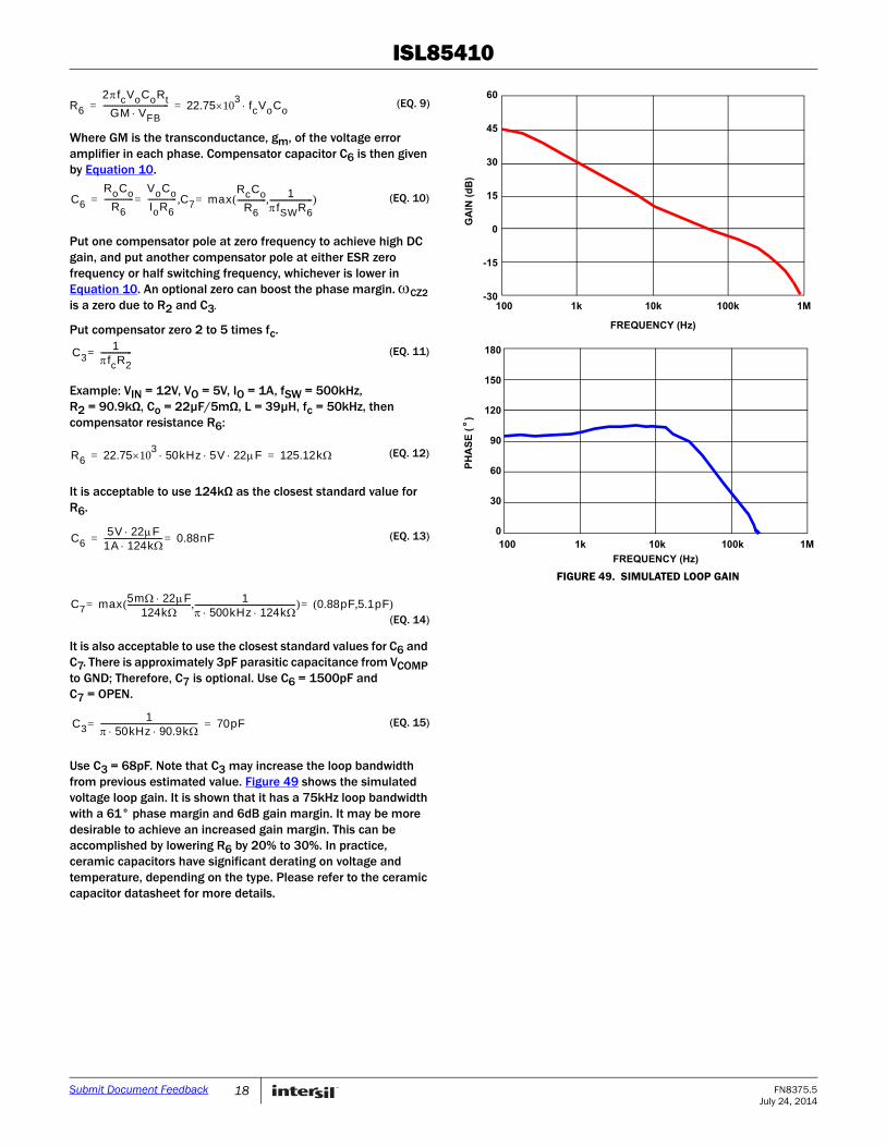
Loop Compensation DesignWhen COMP is not connected to VCC, the COMP pin is active for external loop compensation. The ISL85410 uses constant frequency peak current mode control architecture to achieve a fast loop transient response. An accurate current sensing pilot device in parallel with the upper MOSFET is used for peak current control signal and overcurrent protection. The inductor is not considered as a state variable since its peak current is constant, and the system becomes a single order system. It is much easier to design a type II compensator to stabilize the loop than to implement voltage mode control. Peak current mode control has an inherent input voltage feed-forward function to achieve good line regulation. Figure 47 shows the small signal model of the synchronous buck regulator.
Figure 48 shows the type II compensator and its transfer function is expressed as shown in Equation 8:
where,
Compensator design goal:
High DC gain
Choose loop bandwidth fc less than 100kHz
Gain margin: >10dB
Phase margin: >40°
The compensator design procedure is as follows:
The loop gain at crossover frequency of fc has a unity gain. Therefore, the compensator resistance R6 is determined by Equation 9.
VOUTrippleI
8fSWCOUT
-------------------------------------= (EQ. 6)
VOUTripple I*ESR= (EQ. 7)
dVindILin
ini
+
1:D
+ Li
Co
Rc
-Av(S)
d
Vcomp
Fm
He(S)+
Ti(S)
K
ov
Tv(S)
I
LP
+
1:D
+
Rc
Ro
-Av(S)
RT
Fm
He(S)
T
K
o
T (S)
^ ^
V̂ ^
^
^
^
^
FIGURE 47. SMALL SIGNAL MODEL OF SYNCHRONOUS BUCK REGULATOR
RLP
GA
IN (
VL
OO
P (
S(f
i))
-
+
R6
V
V
Vo
GM
V
C7
-
+
C6
VREF
VFB
Vo
VCOMP
FIGURE 48. TYPE II COMPENSATOR
C3R2
R3
Av S v̂COMP
v̂FB--------------------
GM R3
C6 C7+ R2 R3+ --------------------------------------------------------
1S
cz1-------------+
1S
cz2-------------+
S 1S
cp1-------------+
1S
cp2-------------+
---------------------------------------------------------------==
(EQ. 8)
cz11
R6C6--------------- cz2
1R2C3---------------= cp1
C6 C7+
R6C6C7----------------------- cp2
R2 R3+
C3R2R3-----------------------==,=
17 FN8375.5July 24, 2014
Submit Document Feedback
ISL85410
Where GM is the transconductance, gm, of the voltage error amplifier in each phase. Compensator capacitor C6 is then given by Equation 10.
Put one compensator pole at zero frequency to achieve high DC gain, and put another compensator pole at either ESR zero frequency or half switching frequency, whichever is lower in Equation 10. An optional zero can boost the phase margin. CZ2 is a zero due to R2 and C3
Put compensator zero 2 to 5 times fc.
Example: VIN = 12V, VO = 5V, IO = 1A, fSW = 500kHz, R2 = 90.9kΩ, Co = 22µF/5mΩ, L = 39µH, fc = 50kHz, then compensator resistance R6:
It is acceptable to use 124kΩas theclosest standard value for R6.
It is also acceptable to use the closest standard values for C6 and C7. There is approximately 3pF parasitic capacitance from VCOMP to GND; Therefore, C7 is optional. Use C6 = 1500pF and C7 = OPEN.
Use C3 = 68pF. Note that C3 may increase the loop bandwidth from previous estimated value. Figure 49 shows the simulated voltage loop gain. It is shown that it has a 75kHz loop bandwidth with a 61° phase margin and 6dB gain margin. It may be more desirable to achieve an increased gain margin. This can be accomplished by lowering R6 by 20% to 30%. In practice, ceramic capacitors have significant derating on voltage and temperature, depending on the type. Please refer to the ceramic capacitor datasheet for more details.
R6
2fcVoCoRtGM VFB
---------------------------------- 22.75310 fcVoCo= = (EQ. 9)
C6
RoCoR6
---------------VoCoIoR6--------------- C7 max
RcCoR6
--------------- 1fSWR6----------------------( , )=,== (EQ. 10)
C31
fcR2----------------= (EQ. 11)
R6 22.75310 50kHz 5V 22F 125.12k= = (EQ. 12)
C65V 22 F
1A 124k------------------------------ 0.88nF== (EQ. 13)
C7 max 5m 22F124k
--------------------------------- 1 500kHz 124k ----------------------------------------------------( , ) 0.88pF 5.1pF( , )==
(EQ. 14)
C31
50kHz 90.9k --------------------------------------------------= 70pF= (EQ. 15)
FIGURE 49. SIMULATED LOOP GAIN
60
45
30
15
0
-15
-30100 1k 10k 100k 1M
FREQUENCY (Hz)
180
150
120
90
60
30
0100 1k 10k 100k 1M
FREQUENCY (Hz)
PH
AS
E (°
)G
AIN
(d
B)
18 FN8375.5July 24, 2014
Submit Document Feedback
ISL85410
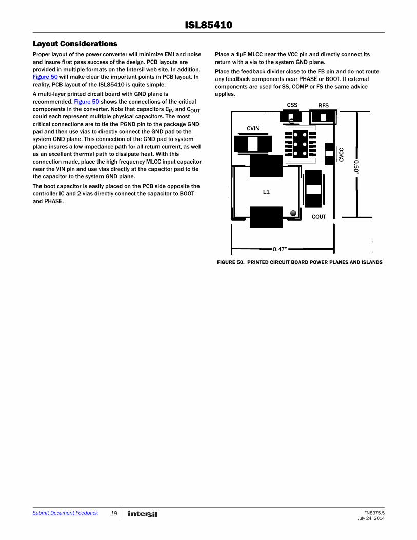
Layout ConsiderationsProper layout of the power converter will minimize EMI and noise and insure first pass success of the design. PCB layouts are provided in multiple formats on the Intersil web site. In addition, Figure 50 will make clear the important points in PCB layout. In reality, PCB layout of the ISL85410 is quite simple.
A multi-layer printed circuit board with GND plane is recommended. Figure 50 shows the connections of the critical components in the converter. Note that capacitors CIN and COUT could each represent multiple physical capacitors. The most critical connections are to tie the PGND pin to the package GND pad and then use vias to directly connect the GND pad to the system GND plane. This connection of the GND pad to system plane insures a low impedance path for all return current, as well as an excellent thermal path to dissipate heat. With this connection made, place the high frequency MLCC input capacitor near the VIN pin and use vias directly at the capacitor pad to tie the capacitor to the system GND plane.
The boot capacitor is easily placed on the PCB side opposite the controller IC and 2 vias directly connect the capacitor to BOOT and PHASE.
Place a 1µF MLCC near the VCC pin and directly connect its return with a via to the system GND plane.
Place the feedback divider close to the FB pin and do not route any feedback components near PHASE or BOOT. If external components are used for SS, COMP or FS the same advice applies.
L1
COUT
CVIN
CSS RFS
CVCC
FIGURE 50. PRINTED CIRCUIT BOARD POWER PLANES AND ISLANDS
RFSCSS
CVIN
L1
COUT
CVC
C
0.5
0”
0.47”
19 FN8375.5July 24, 2014
Submit Document Feedback
ISL85410
Intersil products are manufactured, assembled and tested utilizing ISO9001 quality systems as notedin the quality certifications found at www.intersil.com/en/support/qualandreliability.html
Intersil products are sold by description only. Intersil Corporation reserves the right to make changes in circuit design, software and/or specifications at any time without notice. Accordingly, the reader is cautioned to verify that data sheets are current before placing orders. Information furnished by Intersil is believed to be accurate and reliable. However, no responsibility is assumed by Intersil or its subsidiaries for its use; nor for any infringements of patents or other rights of third parties which may result from its use. No license is granted by implication or otherwise under any patent or patent rights of Intersil or its subsidiaries.
For information regarding Intersil Corporation and its products, see www.intersil.com
For additional products, see www.intersil.com/en/products.html
About IntersilIntersil Corporation is a leading provider of innovative power management and precision analog solutions. The company's products address some of the largest markets within the industrial and infrastructure, mobile computing and high-end consumer markets.
For the most updated datasheet, application notes, related documentation and related parts, please see the respective product information page found at www.intersil.com.
You may report errors or suggestions for improving this datasheet by visiting www.intersil.com/ask.
Reliability reports are also available from our website at www.intersil.com/support
Revision HistoryThe revision history provided is for informational purposes only and is believed to be accurate, but not warranted. Please go to web to make sure you have the latest revision.
DATE REVISION CHANGE
July 24, 2014 FN8375.5 Changed title of Figure 13, on page 9 from “Efficiency vs Load, PWM, VOUT = 5V, L1 = 30µH” to “VOUT Regulation vs Load, PWM, VOUT = 5V, L1 = 30µH”. Replaced Figure Figure 46, on page 16.Updated POD from L12.4x3 to L12.3x4
February 25, 2014 FN8375.4 “Power-On Reset” on page 14 changed 10µA to 2µA.
January 17, 2014 FN8375.3 “Functional Block Diagram” on page 5 changed Internal=50µs, External=230µsto Internal=50µA/V, External=230µA/V and 600mA/Amp to 500mV/A“Detailed Description” on page 14 changed 0.9A to 1.5A“Power-On Reset” on page 14 changed 1µA to 10µA“PWM Control Scheme” on page 14 changed in last paragraph 50µs vs 220µs to 50µA/V vs 230µA/V and 600mA/Amp to 500mV/A in 1st paragraph“Overcurrent Protection” on page 15 changed 0.9A to 1.5A
November 22, 2013 FN8375.2 Initial Release.
20 FN8375.5July 24, 2014
Submit Document Feedback
ISL85410
21 FN8375.5July 24, 2014
Submit Document Feedback
Package Outline DrawingL12.3x412 LEAD DUAL FLAT NO-LEAD PLASTIC PACKAGE
Rev 0, 12/11
BOTTOM VIEW
DETAIL "X"
SIDE VIEW
TYPICAL RECOMMENDED LAND PATTERN
TOP VIEW
located within the zone indicated. The pin #1 identifier may be
Unless otherwise specified, tolerance : Decimal ± 0.05
Tiebar shown (if present) is a non-functional feature.
The configuration of the pin #1 identifier is optional, but must be
between 0.15mm and 0.30mm from the terminal tip.
Dimension applies to the metallized terminal and is measured
Dimensions in ( ) for Reference Only.
Dimensioning and tolerancing conform to ASME Y14.5m-1994.
6.
either a mold or mark feature.
3.
5.
4.
2.
Dimensions are in millimeters.1.
NOTES:
3.00
4.0
0
AB
(4X) 0.10
6PIN 1
INDEX AREA
C 0 . 203 REF
0 . 05 MAX.0 . 00 MIN.
SEE DETAIL "X"
12 1
( 2.80 )
(1.70)
( 12 X 0.25)
(12X 0.60)
( 3.30 ) ( 2.50)
(10x 0.50)
0.10 C
0.08 CSEATING PLANE
0.90 MAX
C
PIN #1
10X 0.50
3.30 ±0.10
12X 0.40 ± 0.05
6
0.1012X 0.25 ±0.05
AM C B
4
2X 2.50
INDEX AREA
7 6
1.70±0.10
Reference document JEDEC MO-229.7.