Embed Size (px)
DESCRIPTION
Â
Citation preview
15Winter 2002 Yield Management Solutions
Defect Management for300 mm and 130 nmTechnologies
Part 3: Another Day, Another Yield Learning Cycle
Kurt Weiner, Todd Henry, Akella Satya, Gaurav Verma, Richard Wu, KLA-Tencor Corporation
Oliver Patterson, Brian Crevasse, Kris Cauffman, William Cauffman, Agere Systems
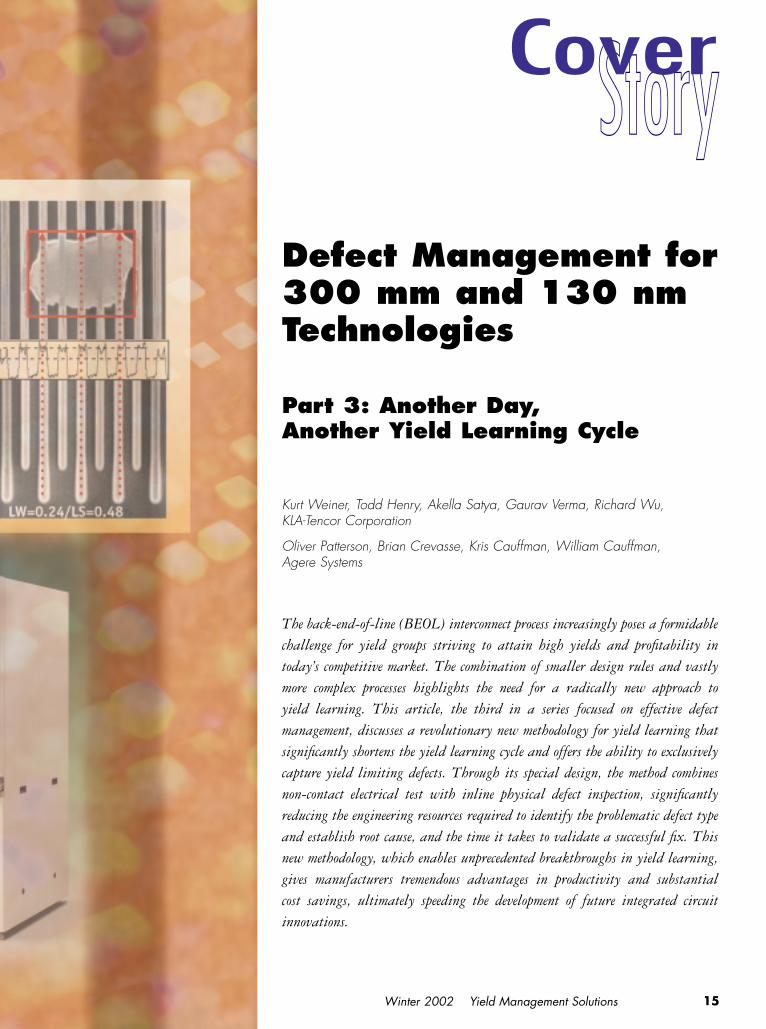
The back-end-of-line (BEOL) interconnect process increasingly poses a formidablechallenge for yield groups striving to attain high yields and profitability intoday’s competitive market. The combination of smaller design rules and vastlymore complex processes highlights the need for a radically new approach to yield learning. This article, the third in a series focused on effective defect management, discusses a revolutionary new methodology for yield learning thatsignificantly shortens the yield learning cycle and offers the ability to exclusivelycapture yield limiting defects. Through its special design, the method combinesnon-contact electrical test with inline physical defect inspection, significantlyreducing the engineering resources required to identify the problematic defect typeand establish root cause, and the time it takes to validate a successful fix. Thisnew methodology, which enables unprecedented breakthroughs in yield learning,gives manufacturers tremendous advantages in productivity and substantial cost savings, ultimately speeding the development of future integrated circuitinnovations.
SSttoorryyCover
16 Winter 2002 Yield Management Solutions
IntroductionSeveral years ago KLA-Tencor recog-nized a critical gap in a fab’s ability tominimize the time-to-market for a newtechnology: the speed and effective-ness of the yield learning methodologyfor the back-end-of-line. In response,KLA-Tencor developed a new approachbased on its powerful e-beam inspec-tion and defect review technologies.
KLA-Tencor’s µLoop technology,which enables faster yield learning,leverages existing engineeringresources to allow earlier technologyintroduction at significantly higheryields. Effective use of this technologyalso results in an accelerated yield rampand higher, mature technology yields.This earlier introduction of technol-ogy, coupled with an accelerated yieldramp, results in increased profitability,as semiconductor manufacturers areable to take advantage of the highermargins that are available early in thelife of new leading edge technologies.
What are the underlying market andtechnology factors driving the tran-sition to this new method?
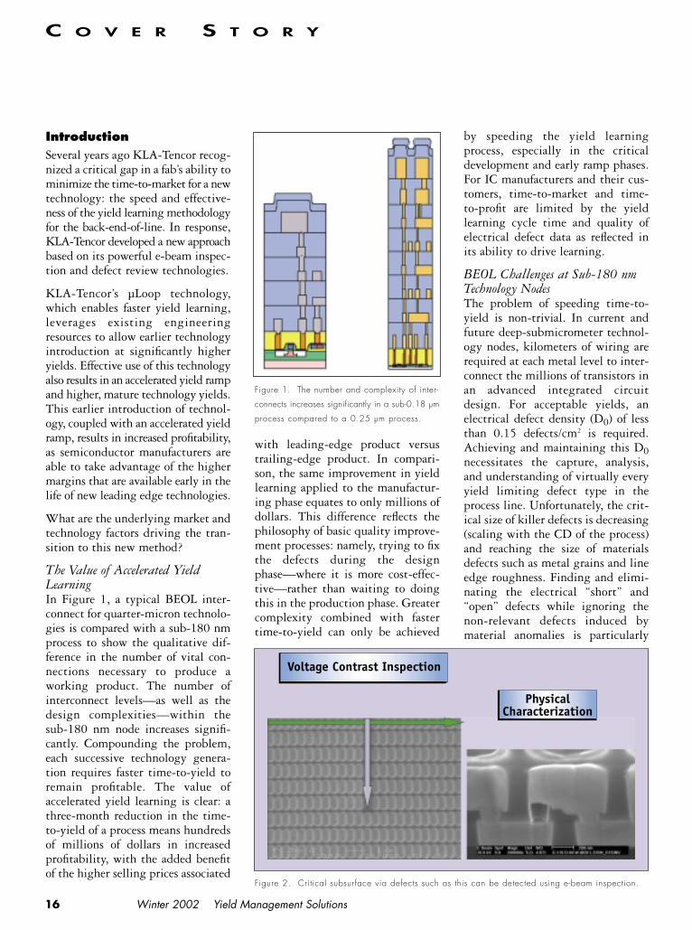
The Value of Accelerated YieldLearningIn Figure 1, a typical BEOL inter-connect for quarter-micron technolo-gies is compared with a sub-180 nmprocess to show the qualitative dif-ference in the number of vital con-nections necessary to produce aworking product. The number ofinterconnect levels—as well as thedesign complexities—within thesub-180 nm node increases signifi-cantly. Compounding the problem,each successive technology genera-tion requires faster time-to-yield toremain profitable. The value ofaccelerated yield learning is clear: athree-month reduction in the time-to-yield of a process means hundredsof millions of dollars in increasedprofitability, with the added benefitof the higher selling prices associated
by speeding the yield learningprocess, especially in the criticaldevelopment and early ramp phases.For IC manufacturers and their cus-tomers, time-to-market and time-to-profit are limited by the yieldlearning cycle time and quality ofelectrical defect data as reflected inits ability to drive learning.
BEOL Challenges at Sub-180 nmTechnology NodesThe problem of speeding time-to-yield is non-trivial. In current andfuture deep-submicrometer technol-ogy nodes, kilometers of wiring arerequired at each metal level to inter-connect the millions of transistors inan advanced integrated circuitdesign. For acceptable yields, anelectrical defect density (D0) of lessthan 0.15 defects/cm2 is required.Achieving and maintaining this D0necessitates the capture, analysis,and understanding of virtually everyyield limiting defect type in theprocess line. Unfortunately, the crit-ical size of killer defects is decreasing(scaling with the CD of the process)and reaching the size of materialsdefects such as metal grains and lineedge roughness. Finding and elimi-nating the electrical “short” and“open” defects while ignoring thenon-relevant defects induced bymaterial anomalies is particularly
with leading-edge product versustrailing-edge product. In compari-son, the same improvement in yieldlearning applied to the manufactur-ing phase equates to only millions ofdollars. This difference reflects thephilosophy of basic quality improve-ment processes: namely, trying to fixthe defects during the designphase—where it is more cost-effec-tive—rather than waiting to doingthis in the production phase. Greatercomplexity combined with fastertime-to-yield can only be achieved
C O V E R S T O R Y
Voltage Contrast Inspection
PhysicalCharacterization
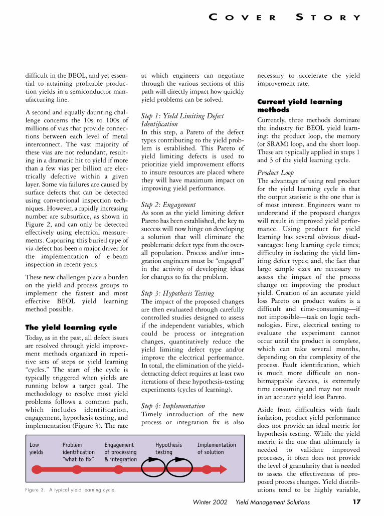
Figure 2. Critical subsurface via defects such as this can be detected using e-beam inspection.
Figure 1. The number and complexity of inter-
connects increases significantly in a sub-0.18 µm
process compared to a 0.25 µm process.
17Winter 2002 Yield Management Solutions
at which engineers can negotiatethrough the various sections of thispath will directly impact how quicklyyield problems can be solved.
Step 1: Yield Limiting DefectIdentificationIn this step, a Pareto of the defecttypes contributing to the yield prob-lem is established. This Pareto ofyield limiting defects is used to prioritize yield improvement effortsto insure resources are placed wherethey will have maximum impact onimproving yield performance.
Step 2: EngagementAs soon as the yield limiting defectPareto has been established, the key tosuccess will now hinge on developinga solution that will eliminate theproblematic defect type from the over-all population. Process and/or inte-gration engineers must be “engaged”in the activity of developing ideasfor changes to fix the problem.
Step 3: Hypothesis TestingThe impact of the proposed changesare then evaluated through carefullycontrolled studies designed to assessif the independent variables, whichcould be process or integrationchanges, quantitatively reduce theyield limiting defect type and/orimprove the electrical performance.In total, the elimination of the yield-detracting defect requires at least twoiterations of these hypothesis-testingexperiments (cycles of learning).
Step 4: ImplementationTimely introduction of the newprocess or integration fix is also
necessary to accelerate the yieldimprovement rate.
Current yield learningmethods Currently, three methods dominatethe industry for BEOL yield learn-ing: the product loop, the memory(or SRAM) loop, and the short loop.These are typically applied in steps 1and 3 of the yield learning cycle.
Product LoopThe advantage of using real productfor the yield learning cycle is thatthe output statistic is the one that isof most interest. Engineers want tounderstand if the proposed changeswill result in improved yield perfor-mance. Using product for yieldlearning has several obvious disad-vantages: long learning cycle times;difficulty in isolating the yield lim-iting defect types; and, the fact thatlarge sample sizes are necessary toassess the impact of the processchange on improving the productyield. Creation of an accurate yieldloss Pareto on product wafers is adifficult and time-consuming—ifnot impossible—task on logic tech-nologies. First, electrical testing toevaluate the experiment cannotoccur until the product is complete,which can take several months,depending on the complexity of theprocess. Fault identification, whichis much more difficult on non-bitmappable devices, is extremelytime consuming and may not resultin an accurate yield loss Pareto.
Aside from difficulties with faultisolation, product yield performancedoes not provide an ideal metric forhypothesis testing. While the yieldmetric is the one that ultimately isneeded to validate improvedprocesses, it often does not providethe level of granularity that is neededto assess the effectiveness of pro-posed process changes. Yield distrib-utions tend to be highly variable,
difficult in the BEOL, and yet essen-tial to attaining profitable produc-tion yields in a semiconductor man-ufacturing line.
A second and equally daunting chal-lenge concerns the 10s to 100s ofmillions of vias that provide connec-tions between each level of metalinterconnect. The vast majority ofthese vias are not redundant, result-ing in a dramatic hit to yield if morethan a few vias per billion are elec-trically defective within a givenlayer. Some via failures are caused bysurface defects that can be detectedusing conventional inspection tech-niques. However, a rapidly increasingnumber are subsurface, as shown inFigure 2, and can only be detectedeffectively using electrical measure-ments. Capturing this buried type ofvia defect has been a major driver forthe implementation of e-beaminspection in recent years.
These new challenges place a burdenon the yield and process groups toimplement the fastest and mosteffective BEOL yield learningmethod possible.
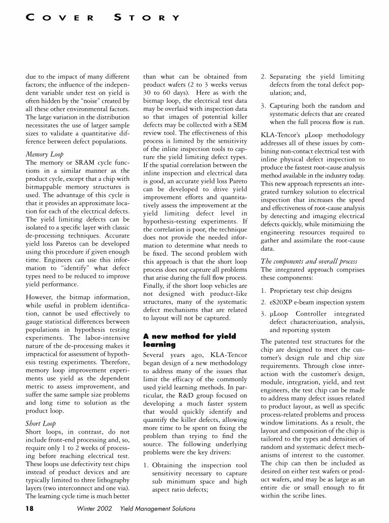
The yield learning cycleToday, as in the past, all defect issuesare resolved through yield improve-ment methods organized in repeti-tive sets of steps or yield learning“cycles.” The start of the cycle istypically triggered when yields arerunning below a target goal. Themethodology to resolve most yieldproblems follows a common path,which includes identification,engagement, hypothesis testing, andimplementation (Figure 3). The rate
C O V E R S T O R Y
Low Problem Engagement Hypothesis Implementationyields identification of processing testing of solution
“what to fix” & integration
Figure 3. A typical yield learning cycle.
18 Winter 2002 Yield Management Solutions
2. Separating the yield limitingdefects from the total defect pop-ulation; and,
3. Capturing both the random andsystematic defects that are createdwhen the full process flow is run.
KLA-Tencor’s µLoop methodologyaddresses all of these issues by com-bining non-contact electrical test withinline physical defect inspection toproduce the fastest root-cause analysismethod available in the industry today.This new approach represents an inte-grated turnkey solution to electricalinspection that increases the speedand effectiveness of root-cause analysisby detecting and imaging electricaldefects quickly, while minimizing theengineering resources required togather and assimilate the root-causedata.
The components and overall processThe integrated approach comprisesthese components:
1. Proprietary test chip designs
2. eS20XP e-beam inspection system
3. µLoop Controller integrateddefect characterization, analysis,and reporting system
The patented test structures for thechip are designed to meet the cus-tomer’s design rule and chip sizerequirements. Through close inter-action with the customer’s design,module, integration, yield, and testengineers, the test chip can be madeto address many defect issues relatedto product layout, as well as specificprocess-related problems and processwindow limitations. As a result, thelayout and composition of the chip istailored to the types and densities ofrandom and systematic defect mech-anisms of interest to the customer.The chip can then be included asdesired on either test wafers or prod-uct wafers, and may be as large as anentire die or small enough to fitwithin the scribe lines.
due to the impact of many differentfactors; the influence of the indepen-dent variable under test on yield isoften hidden by the “noise” created byall these other environmental factors.The large variation in the distributionnecessitates the use of larger samplesizes to validate a quantitative dif-ference between defect populations.
Memory LoopThe memory or SRAM cycle func-tions in a similar manner as theproduct cycle, except that a chip withbitmappable memory structures isused. The advantage of this cycle isthat it provides an approximate loca-tion for each of the electrical defects.The yield limiting defects can beisolated to a specific layer with classicde-processing techniques. Accurateyield loss Paretos can be developedusing this procedure if given enoughtime. Engineers can use this infor-mation to “identify” what defecttypes need to be reduced to improveyield performance.
However, the bitmap information,while useful in problem identifica-tion, cannot be used effectively togauge statistical differences betweenpopulations in hypothesis testingexperiments. The labor-intensivenature of the de-processing makes itimpractical for assessment of hypoth-esis testing experiments. Therefore,memory loop improvement experi-ments use yield as the dependentmetric to assess improvement, andsuffer the same sample size problemsand long time to solution as theproduct loop.
Short LoopShort loops, in contrast, do notinclude front-end processing and, so,require only 1 to 2 weeks of process-ing before reaching electrical test.These loops use defectivity test chipsinstead of product devices and aretypically limited to three lithographylayers (two interconnect and one via).The learning cycle time is much better
than what can be obtained fromproduct wafers (2 to 3 weeks versus30 to 60 days). Here as with thebitmap loop, the electrical test datamay be overlaid with inspection dataso that images of potential killerdefects may be collected with a SEMreview tool. The effectiveness of thisprocess is limited by the sensitivityof the inline inspection tools to cap-ture the yield limiting defect types.If the spatial correlation between theinline inspection and electrical datais good, an accurate yield loss Paretocan be developed to drive yieldimprovement efforts and quantita-tively assess the improvement at theyield limiting defect level inhypothesis-testing experiments. Ifthe correlation is poor, the techniquedoes not provide the needed infor-mation to determine what needs tobe fixed. The second problem withthis approach is that the short loopprocess does not capture all problemsthat arise during the full flow process.Finally, if the short loop vehicles arenot designed with product-likestructures, many of the systematicdefect mechanisms that are relatedto layout will not be captured.
A new method for yieldlearning Several years ago, KLA-Tencorbegan design of a new methodologyto address many of the issues thatlimit the efficacy of the commonlyused yield learning methods. In par-ticular, the R&D group focused ondeveloping a much faster systemthat would quickly identify andquantify the killer defects, allowingmore time to be spent on fixing theproblem than trying to find thesource. The following underlyingproblems were the key drivers:
1. Obtaining the inspection toolsensitivity necessary to capturesub minimum space and highaspect ratio defects;
C O V E R S T O R Y

19Winter 2002 Yield Management Solutions
of test structures optimized for per-formance and speed-of-inspectionusing KLA-Tencor’s e-beam technol-ogy (see the sidebar on voltage con-trast inspection). By using a set ofproprietary Area-Accelerated™ teststructures, throughput enhancementsof 10 to 25 times that of standardarea-based e-beam inspections areavailable. A simplified example ofthis new class of test structure isshown in Figure 5. In this structure,
which addresses interconnect opensand shorts, grounded and floating tinesare inter-digitated similar to a comb.Leveraging the properties of voltagecontrast inspection discussed in thesidebar, these new test structuresrequire inspection of only a smallregion at the bottom of the teststructure. Electrical defects presentalong the length of the tine are trans-mitted down the tine and sensedthrough a large voltage contrast defectthat appears as a deviation in thenormal alternating grounded/floatingtine pattern. Through this patenteddesign both shorts and opens can bedetected. The CD of the process setsthe minimum sensitivity of the teststructure measurement. Therefore,the test structures provide highthroughput (through sampling) athigh sensitivity (through voltagecontrast defect amplification).
Grounded via chains are an alternatetype of test structure that includelarge numbers of individual vias,offering a quantitative measurementof any systematic issue that causes aburied open in the via structure (alsosee the sidebar on random and sys-tematic defect types). These structuresare advantageous in that probing ofeach individual via is not required;again a voltage contrast defect willbe detected at the bottom of the teststructure if any via is open.
Figure 4 shows a general schematicof the µLoop cycle. The test chips aremanufactured with the standard BEOLwafer processing. Upon completion ofthe fabrication of each interconnectlayer, the eS20XP e-beam inspectionsystem first captures the criticaldefects, and then the µLoop Con-troller characterizes the defects andprovides customized defect and yieldsummary reports. These reports eitherhelp identify what defect problemneeds to be fixed, or help assess theeffectiveness of a process and/or inte-gration change on eliminating theproblematic defect type (steps 1 and 3in the yield learning cycle describedearlier). Experiments using the µLoopvehicle continue until the yieldproblem is resolved. Upon resolutionof the current problem, resources arerefocused on the next item on thePareto.
The test structures and e-beaminspectionThe µLoop solution is based on theconcept of voltage contrast inspection
C O V E R S T O R Y
Figure 4. µLoop uses custom test structures, e-beam inspection and an integrated defect charac-
terization and yield analysis system to complete the yield learning cycle.
Intralayer Shorts/OpensInterlayer Shorts Via Opens (chains) Via Opens (single)
Figure 5. This new class of test structure takes advantage of the properties inherent to voltage
contrast inspection.

20
Another key advantage of thismethodology is that it is non-con-tact. Because there is no need foractual probing, there is less risk ofcontamination induced by the mea-surement, and thus the same wafercan be probed at all levels of theinterconnect process.
µLoop Inspection MethodologyThe complete µLoop inspection usesa three-step process:
1. Assess
2. Identify
3. Classify
Winter 2002 Yield Management Solutions
Step 1) AssessThe assess step is an Area-Accelerated e-beam inspection thatquickly identifies the electrical defectsacross the entire wafer. The through-put of this inspection is maximizedthrough the design of the test chip;due to the nature of voltage contrast,a high-sensitivity inspection is notrequired, and all of the VC signa-tures for a particular type of struc-ture can be seen by sampling a smallarea of the chip. Because the teststructure is divided into thousandsof individual tines, rather than alarge-area comb, the exact locationof the defect in one dimension can bequickly identified. During this scan,both electrical and any type of phys-ical defect in the inspected area aredetected. Because physical defects areconsidered non-relevant in this stepof the µLoop methodology, they arefiltered out by the µLoop Controller,and the final result is a list of theelectrical defects and their locations.
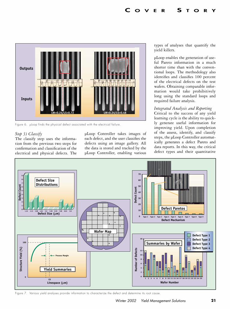
Step 2) IdentifyThe identify step finds the associatedphysical defects (see Figure 6). Theprevious step provided the x-coordi-nate of the physical defect, andalthough the y-location is not exact, itis bounded by the test structure height.Using this information, a customrecipe is automatically generated foreach wafer that is assessed. To facilitatethe identify inspection, the wafer isrotated 90 degrees. This custom recipeprovides an inspection test plan thatincludes only a small region aroundeach defect detected during theassessment scan. Because the numberof electrical defects is usually quitelow, the total area inspected is verysmall (typically much less than 1percent of the total wafer). The smallinspected area helps to offset theimpact on the throughput of thehigher sensitivity conditionsrequired for determining the exactlocation of the physical defects causingthe critical electrical failures.
C O V E R S T O R Y
Voltage contrast inspection Voltage contrast is inherent to all e-beam inspection technologies, but is onlycreated under specific kinds of conditions. During inspection, a conductivematerial is exposed to a beam of electrons, and a number of the incidentelectrons collide with the atoms of the metal. A certain fraction of the collisions (depending on the type of metal) produce “secondary” electrons,which are re-emitted from the surface of the conductor at a much lowerenergy than that of the incident beam. This fraction of secondary electrons isalso a function of the incident or “landing” energy of the primary electronbeam and can be controlled to be less than or greater than one. If the con-ductor is isolated or “floating,” the difference in secondary electrons emittedversus primary electrons absorbed produces a net charge over the entireconducting node. When the landing energy is set so that the charge accu-mulated on the floating conductor is positive (more secondary electronsemitted than primary electrons absorbed), the node builds up a charge untilthe potential is large enough to inhibit the emission of more secondaryelectrons, and the node attains a static voltage. Secondary electrons cancomprise up to 80 percent of the imaged electrons so, in this situation, thenode can appear dark when imaged. In contrast, if the node is connected toa source of electrons (such as a grounded substrate), electrons from thesource can flow to neutralize the charge build-up. This “grounded” nodenever builds a positive potential and so appears brighter than the floatingnode when imaged. This brightness difference between adjacent nodes canbe used to indicate the relative voltage difference between the nodes, andcan indicate the presence of an electrical defect.
Typically, voltage contrast detection is used to complement physical defectdetection in an e-beam inspector by providing some electrical informationon the product defectivity. Use of voltage contrast defect detection alone toanalyze overall product electrical yield is a complex process. However, voltagecontrast can be used effectively with specially designed test structures topreferentially detect electrical defects, while rejecting physical defects that donot cause electrical failures. In this mode, voltage contrast defect detectionhas two important advantages: first, the presence of voltage contrast is anaccurate indicator of an electrical failure on the node, providing a means forelectrical inspection. Second, because a conductive node assumes the samepotential across the entire node very quickly, regardless of size, voltage contrast can be used to both amplify very small physical defects into verylarge voltage contrast defects and to transmit the defect signature to a common region within the test structure. Using the defect amplificationand transmission traits of voltage contrast, a class of test structures that ishighly optimized for throughput and sensitivity can be designed.
21Winter 2002 Yield Management Solutions
Step 3) ClassifyThe classify step uses the informa-tion from the previous two steps forconfirmation and classification of theelectrical and physical defects. The
µLoop Controller takes images ofeach defect, and the user classifies thedefects using an image gallery. Allthe data is stored and tracked by theµLoop Controller, enabling various
types of analyses that quantify theyield killers.
µLoop enables the generation of use-ful Pareto information in a muchshorter time than with the conven-tional loops. The methodology alsoidentifies and classifies 100 percentof the electrical defects on the testwafers. Obtaining comparable infor-mation would take prohibitivelylong using the standard loops andrequired failure analysis.
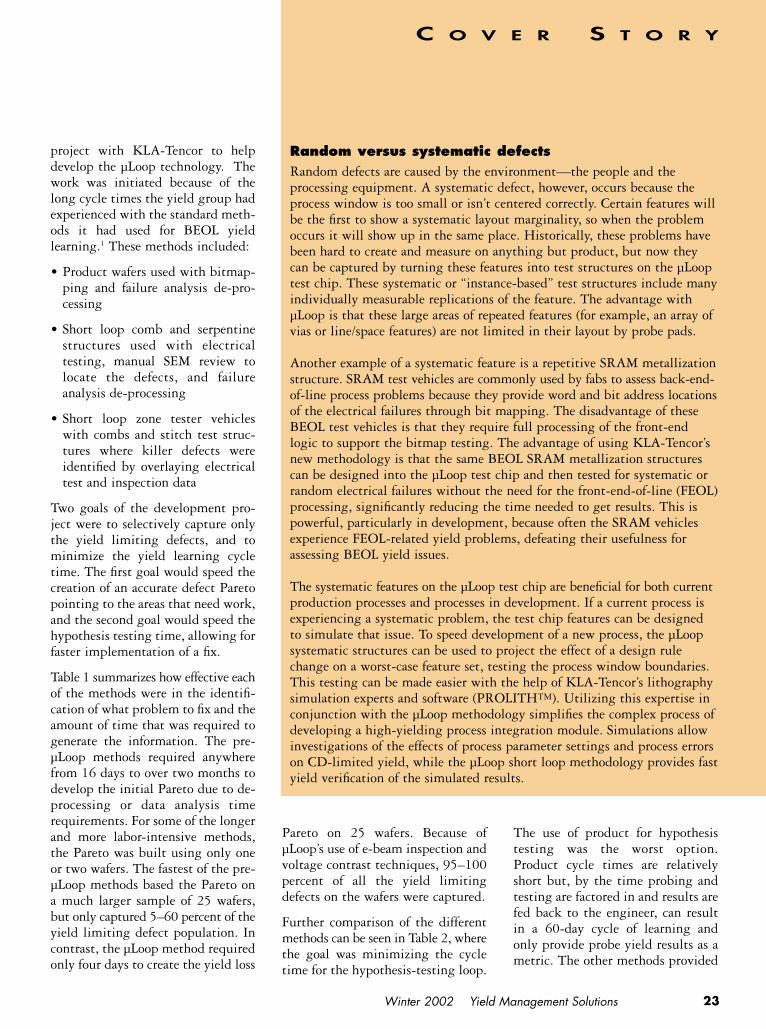
Integrated Analysis and ReportingCritical to the success of any yieldlearning cycle is the ability to quick-ly generate useful information forimproving yield. Upon completionof the assess, identify, and classifysteps, the µLoop Controller automat-ically generates a defect Pareto anddata reports. In this way, the criticaldefect types and their quantitative
C O V E R S T O R Y
Outputs
Inputs
LW=0.24/LS=0.72
251.00 248.00
15.00 13.00
LW=0.24/LS=0.48
Figure 6. µLoop finds the physical defect associated with the electrical failure.
Process Margin
Linespace (µm)
100
CD0
Stru
ctur
e Yi
eld
(%)
Yield Summaries
18
12
10
8
6
4
2
01 2 3 4 6 7 8 9 10 11 15 16 17 18 19 21 22 23 24 25
Wafer Number
Num
ber
of D
efec
ts
70
60
50
40
30
20
10
0 Type 1 Type 2 Type 3 Type 4 Type 5 Type 6 Type 7 Type 8 Type 9
Defect Mechanism
Defe
ct C
ount
9
8
7
6
5
4
3
2
1
01.16 2.12 3.08 4.04 5.0 5.96 6.92 7.88 8.84 9.8
Defect Size (µm)
Defe
ct C
ount
Defect SizeDistributions
Defect Paretos
Defect Type 1Defect Type 2Defect Type 3Defect Type 4
Summaries by Wafer
Wafer Map
Figure 7. Various yield analyses provide information to characterize the defect and determine its root cause.
22
contributions to yield loss are imme-diately known, eliminating days, oreven months, from the standardyield learning cycle. Analyses are alsoprepared based on the data stored bythe system, including yield sum-maries, defect densities, defectimages, defect size distributions,wafer maps (for spatial signaturestudy), and defect type summariesfor multiple wafers (see Figure 7).These reports are configurable andcan be automatically e-mailed to adistribution list if desired.
Application to yieldimprovement effortsHow should a fab use the powerfuldata provided by µLoop?
Providing FocusA typical problem less-experiencedyield groups run into is having toomuch data and not being sure whichproblems to focus on in order tomaximize the rate of yield improve-ment. Other groups become ineffec-tive when they try to resolve all yieldproblems. The data from µLoop canbe used to bring a more systematicand structured approach to yieldimprovement problems. This newmethodology results in a defect typeyield loss Pareto that quantifies thelargest contributors to yield loss.The best way to proceed is to use theinformation and systematically focuson the defects that are causing the
greatest percentage of yield loss. Asproblems are resolved, the engineerrefocuses on the next largest contrib-utors on the yield loss Pareto.
Yield LearningThe main use for µLoop (and the oneprimarily discussed in this article) isthe yield learning application, wherethe goal is to rapidly identify and fixproblems. Here, all three steps (assess,identify, classify) are used, along witha full report including the D0, Pareto,images, etc. The case studies in thesubsequent sections of this articleare all examples of using µLoop forthe yield learning application.
Yield MonitoringInline yield monitoring is anotherapplication of µLoop. The othershort loop methods do not provideinline electrical testing information;their testing comes at the end of theline, when processing is complete.The non-contact nature of µLoopallows electrical testing after eachcomplete interconnect level. In thisapplication, the three-step method-ology is abbreviated to only the firststep—the assess step—which givesthe density of electrical failures. Ifthis density is below a certain value,no further action is needed, and asimple inline monitoring report isgenerated. If there is an excursion ofelectrical failures, then the other twosteps can be completed, generatingthe full set of information, with a
Winter 2002 Yield Management Solutions
Pareto and images to help find thesource of the excursion.
Providing Evidence to Help EngageProcess GroupsThe yield group can use the infor-mation from µLoop to thoroughlycharacterize the primary killer defecttype, with the ultimate goal of per-suading the appropriate processand/or integration group(s) to engageand dedicate resources to fix theproblem. The difficulty of convincingthe process groups to assist should notbe underestimated as a potential hurdlein the yield improvement process.Often, the only way to accomplish itis to have thorough and quantitativecharacterization data showing specif-ically what percentage of the yield-limiting defects came from thatgroup’s process or equipment. Themain results from the µLoopmethodology (number of physicaldefects causing electrical failure, anda Pareto of those defect types) pro-vide the convincing evidence needed.
Tuning Inline InspectionsAnother use for the uLoop data is toevaluate inline optical inspectionrecipes for their ability to captureyield-limiting defects. The defects,captured with inline optical andlaser inspections can be character-ized and compared with the yieldlimiting defects captured with theµLoop process. Inspection recipes canbe optimized for use on productwafers to maximize the capture oftop yield limiting defects capturewith the µLoop process.
(See the sidebar on root cause analy-sis for further information about theintegration of µLoop with inlineinspection techniques.)
Comparison of the newmethod to previous methodsAgere Systems in Orlando, Florida,participated in a joint development
C O V E R S T O R Y
Root-cause analysis In some situations, images of a defect are all that are required to know itssource. Some yield and process groups have built up expertise over a periodof time that allows them to determine root cause accurately based only on adefect Pareto. But in many situations, particularly with new processes andprocessing equipment, that luxury is not available.
Using the µLoop methodology in conjunction with inline inspections canaccurately identify the specific layer at which the killer physical defects occur.All critical layers of the test wafer are inspected with KLA-Tencor opticaland/or e-beam tools, and then µLoop defect locations are overlaid with theinline inspection defect locations to determine the root cause.
23Winter 2002 Yield Management Solutions
project with KLA-Tencor to helpdevelop the µLoop technology. Thework was initiated because of thelong cycle times the yield group hadexperienced with the standard meth-ods it had used for BEOL yieldlearning.1 These methods included:
• Product wafers used with bitmap-ping and failure analysis de-pro-cessing
• Short loop comb and serpentinestructures used with electricaltesting, manual SEM review tolocate the defects, and failureanalysis de-processing
• Short loop zone tester vehicleswith combs and stitch test struc-tures where killer defects wereidentified by overlaying electricaltest and inspection data
Two goals of the development pro-ject were to selectively capture onlythe yield limiting defects, and tominimize the yield learning cycletime. The first goal would speed thecreation of an accurate defect Paretopointing to the areas that need work,and the second goal would speed thehypothesis testing time, allowing forfaster implementation of a fix.
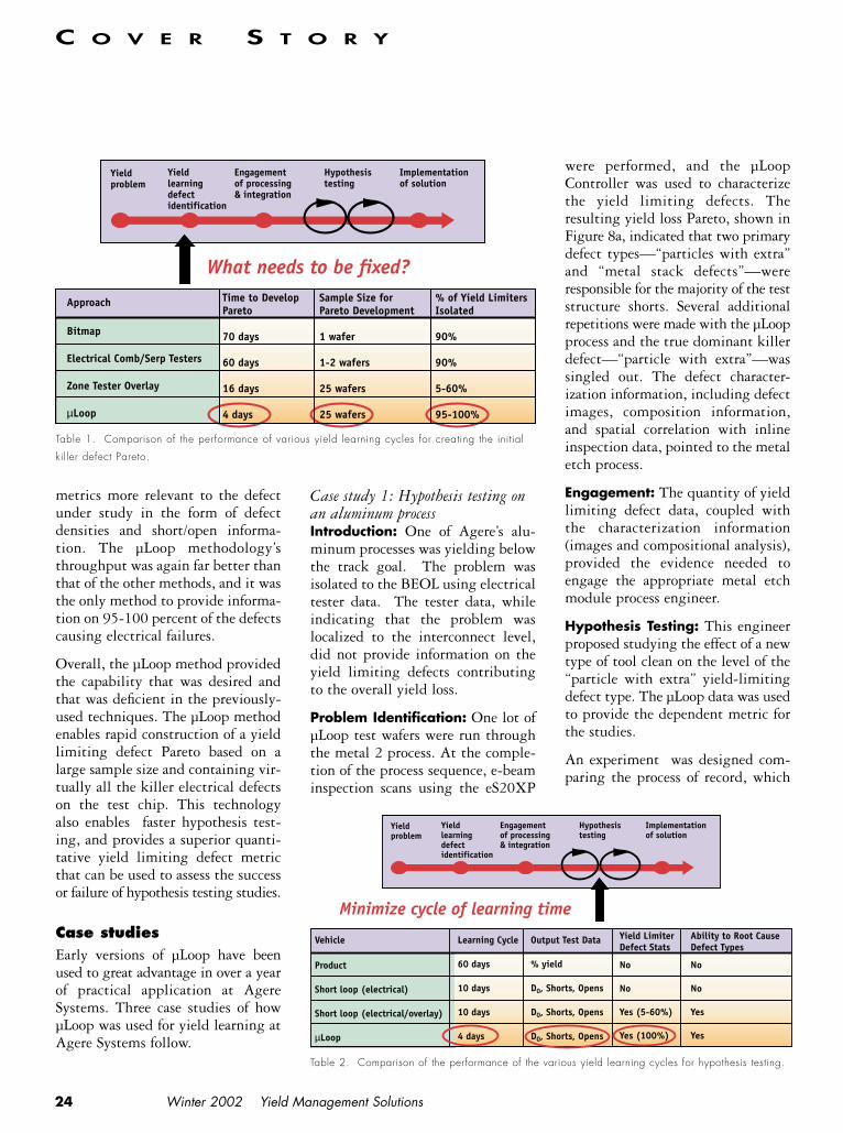
Table 1 summarizes how effective eachof the methods were in the identifi-cation of what problem to fix and theamount of time that was required togenerate the information. The pre-µLoop methods required anywherefrom 16 days to over two months todevelop the initial Pareto due to de-processing or data analysis timerequirements. For some of the longerand more labor-intensive methods,the Pareto was built using only oneor two wafers. The fastest of the pre-µLoop methods based the Pareto ona much larger sample of 25 wafers,but only captured 5–60 percent of theyield limiting defect population. Incontrast, the µLoop method requiredonly four days to create the yield loss
Pareto on 25 wafers. Because ofµLoop’s use of e-beam inspection andvoltage contrast techniques, 95–100percent of all the yield limitingdefects on the wafers were captured.
Further comparison of the differentmethods can be seen in Table 2, wherethe goal was minimizing the cycletime for the hypothesis-testing loop.
The use of product for hypothesistesting was the worst option.Product cycle times are relativelyshort but, by the time probing andtesting are factored in and results arefed back to the engineer, can resultin a 60-day cycle of learning andonly provide probe yield results as ametric. The other methods provided
Random versus systematic defects Random defects are caused by the environment—the people and the processing equipment. A systematic defect, however, occurs because theprocess window is too small or isn’t centered correctly. Certain features willbe the first to show a systematic layout marginality, so when the problemoccurs it will show up in the same place. Historically, these problems havebeen hard to create and measure on anything but product, but now theycan be captured by turning these features into test structures on the µLooptest chip. These systematic or “instance-based” test structures include manyindividually measurable replications of the feature. The advantage withµLoop is that these large areas of repeated features (for example, an array ofvias or line/space features) are not limited in their layout by probe pads.
Another example of a systematic feature is a repetitive SRAM metallizationstructure. SRAM test vehicles are commonly used by fabs to assess back-end-of-line process problems because they provide word and bit address locationsof the electrical failures through bit mapping. The disadvantage of theseBEOL test vehicles is that they require full processing of the front-endlogic to support the bitmap testing. The advantage of using KLA-Tencor’snew methodology is that the same BEOL SRAM metallization structurescan be designed into the µLoop test chip and then tested for systematic orrandom electrical failures without the need for the front-end-of-line (FEOL)processing, significantly reducing the time needed to get results. This ispowerful, particularly in development, because often the SRAM vehiclesexperience FEOL-related yield problems, defeating their usefulness forassessing BEOL yield issues.
The systematic features on the µLoop test chip are beneficial for both currentproduction processes and processes in development. If a current process isexperiencing a systematic problem, the test chip features can be designedto simulate that issue. To speed development of a new process, the µLoopsystematic structures can be used to project the effect of a design rulechange on a worst-case feature set, testing the process window boundaries.This testing can be made easier with the help of KLA-Tencor’s lithographysimulation experts and software (PROLITH™). Utilizing this expertise inconjunction with the µLoop methodology simplifies the complex process ofdeveloping a high-yielding process integration module. Simulations allowinvestigations of the effects of process parameter settings and process errorson CD-limited yield, while the µLoop short loop methodology provides fastyield verification of the simulated results.
C O V E R S T O R Y
24
metrics more relevant to the defectunder study in the form of defectdensities and short/open informa-tion. The µLoop methodology’sthroughput was again far better thanthat of the other methods, and it wasthe only method to provide informa-tion on 95-100 percent of the defectscausing electrical failures.
Overall, the µLoop method providedthe capability that was desired andthat was deficient in the previously-used techniques. The µLoop methodenables rapid construction of a yieldlimiting defect Pareto based on alarge sample size and containing vir-tually all the killer electrical defectson the test chip. This technologyalso enables faster hypothesis test-ing, and provides a superior quanti-tative yield limiting defect metricthat can be used to assess the successor failure of hypothesis testing studies.
Case studiesEarly versions of µLoop have beenused to great advantage in over a yearof practical application at AgereSystems. Three case studies of howµLoop was used for yield learning atAgere Systems follow.
Case study 1: Hypothesis testing onan aluminum processIntroduction: One of Agere’s alu-minum processes was yielding belowthe track goal. The problem wasisolated to the BEOL using electricaltester data. The tester data, whileindicating that the problem waslocalized to the interconnect level,did not provide information on theyield limiting defects contributingto the overall yield loss.
Problem Identification: One lot ofµLoop test wafers were run throughthe metal 2 process. At the comple-tion of the process sequence, e-beaminspection scans using the eS20XP
Winter 2002 Yield Management Solutions
were performed, and the µLoopController was used to characterizethe yield limiting defects. Theresulting yield loss Pareto, shown inFigure 8a, indicated that two primarydefect types—“particles with extra”and “metal stack defects”—wereresponsible for the majority of the teststructure shorts. Several additionalrepetitions were made with the µLoopprocess and the true dominant killerdefect—“particle with extra”—wassingled out. The defect character-ization information, including defectimages, composition information,and spatial correlation with inlineinspection data, pointed to the metaletch process.
Engagement: The quantity of yieldlimiting defect data, coupled withthe characterization information(images and compositional analysis),provided the evidence needed toengage the appropriate metal etchmodule process engineer.
Hypothesis Testing: This engineerproposed studying the effect of a newtype of tool clean on the level of the“particle with extra” yield-limitingdefect type. The µLoop data was usedto provide the dependent metric forthe studies.
An experiment was designed com-paring the process of record, which
Yieldproblem
Yieldlearningdefectidentification
Engagementof processing& integration
Hypothesistesting
Implementationof solution
What needs to be fixed?Time to DevelopPareto
70 days
60 days
16 days
4 days
Approach
Bitmap
Electrical Comb/Serp Testers
Zone Tester Overlay
µLoop
Sample Size forPareto Development
1 wafer
1-2 wafers
25 wafers
25 wafers
% of Yield LimitersIsolated
90%
90%
5-60%
95-100%
Yieldproblem
Yieldlearningdefectidentification
Engagementof processing& integration
Hypothesistesting
Implementationof solution
Minimize cycle of learning time
Learning Cycle
60 days
10 days
10 days
4 days
Vehicle
Product
Short loop (electrical)
Short loop (electrical/overlay)
µLoop
Output Test Data
% yield
D0, Shorts, Opens
D0, Shorts, Opens
D0, Shorts, Opens
Yield LimiterDefect Stats
No
No
Yes (5-60%)
Yes (100%)
Ability to Root CauseDefect Types
No
No
Yes
Yes
Table 1. Comparison of the performance of various yield learning cycles for creating the initial
killer defect Pareto.
Table 2. Comparison of the performance of the various yield learning cycles for hypothesis testing.
C O V E R S T O R Y

25Winter 2002 Yield Management Solutions
ran on tool A, with the new “in-situ”cleaning process, which ran on toolB. The metric for quantifying theresults was the density of “particlewith extra” defects on the µLoop testchips. Initially, one lot was split,with the wafer processing spread outover a period of time to evaluate theeffect of “chamber time since lastmajor tool clean” on the level ofyield limiting “particle with extra”defects.
The results in Figure 8b showeddegradation in the standard cleantool as more wafers were processedthrough it, leading to an increase in the“particle with extra” defect density.
In contrast, the tool with the exper-imental new clean did not show anyincrease over time. The same lot wasused again with the µLoop method-ology at the next metal layer; and, theadditional data confirmed the initialresults. Paretos were generated usingµLoop before and after this processchange was implemented. Figure 8cshows how the density killer defectschanged over this time period. Theimprovement was very clear.
Subsequently, “particles with extra”were still the dominant killer defecttype on the Pareto, though at a muchlower level, but now only a few wafersper lot showed high counts of thisdefect type. Additional µLoop exper-iments led to the discovery of astrong correlation between a certain
process variable and the “particlewith extra” defect count as illustratedin Figure 8d. Note, that for the datashown in Figure 8d, the correlationbetween the total number of killerdefects and this process variable wasnot significant because of an excur-sion of tungsten puddles; thisdemonstrates the value of being ableto break down the yield loss bydefect type. A process adjustment tokeep the level of this certain processvariable down was devised andproven in using µLoop.
Implementation: The decision wasmade to modify the process of recordto include the in-situ clean basedprimarily on the results obtained usingthe uLoop technology. At the time ofthe change, the results from productdata were inconclusive. µLoop greatlyaccelerated the implementation phasefor this first process change. The second change did not require boardapproval and was implemented soonafter the compelling results fromµLoop were obtained.
Summary: µLoop was used to quan-tify the contributions of the variousdefect types to the overall yield lossand to pinpoint the area needing themost work. Next, it was used to testseveral process improvements and theirability to reduce the level of yieldlimiting defects, and to track theireffectiveness over time. This studyhighlights how the use of the µLoopprocess offers a cycle of learning at
Defe
ct D
ensi
ty (
cm2 )
Defect Class
ParticleWithExtra
Stack Extra WPuddle
NotFound
Figure 8a. Results from µLoop showing the initial yield loss Pareto.
Part
icle
wit
h Ex
tra
Dens
ity
Wafer Count0 100 200 300
In-situ CleanNo Clean
Figure 8b. Results from µLoop showing the
degradation of the standard clean process
compared with the new clean.
1 2 3 4 5 6 7 8 9 10 11 12 13 14 15 16
April/May June/JulyLot
No In-situ Clean In-situ Clean
0.2
0.18
0.16
0.14
0.12
0.1
0.08
0.06
0.04
0.02
0
Defe
ct D
ensi
ty (
cm2 )
Etch Particle With Extra*W puddlesDeep or Litho Particle With ExtraStackOther * Defect of Interest
Figure 8c. Results from µLoop showing the
decrease in the critical killer defect type after
the implementation of the new clean.
Proc
ess
Vari
able
X (
Wat
t)
eS20
Par
ticl
e w
ith
Extr
a (P
WE)
300
250
200
150
100
50
0
18
15
12
9
6
3
00 2 4 6 8 10 12
Wafer # (Etch Sequence)
Process Variable XPWE's
Figure 8d. By-wafer correlation between
“particles with extra” and a process variable.
C O V E R S T O R Y
26
each interconnect level for a particu-lar lot. It led to a 4x improvement inthe time needed to implement theseprocess changes. With µLoop, thesechanges were implemented in onlyone and a half months; using theconventional methods they wouldhave taken at least six months.
Case study 2: Capture of a system-atic problem on an aluminum processIntroduction: The practice of peri-odically running µLoops for a numberof technologies to track and charac-terize the BEOL yield loss Pareto wasinstituted early in 2001 at AgereSystems. Often, these same wafers arealso used for hypothesis testingexperiments. The ability of the µLoopmethodology to break down yieldloss by defect type allows the same lotof data to be used for both purposes.
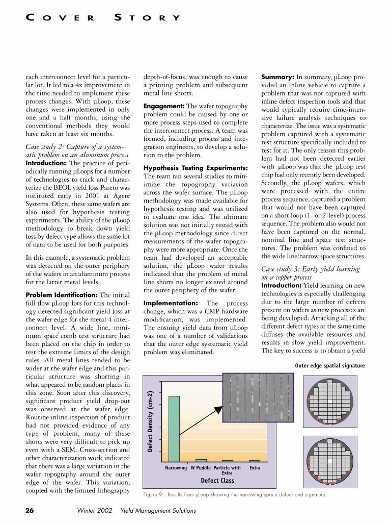
In this example, a systematic problemwas detected on the outer peripheryof the wafers in an aluminum processfor the latter metal levels.
Problem Identification: The initialfull flow µLoop lots for this technol-ogy detected significant yield loss atthe wafer edge for the metal 4 inter-connect level. A wide line, mini-mum space comb test structure hadbeen placed on the chip in order totest the extreme limits of the designrules. All metal lines tended to bewider at the wafer edge and this par-ticular structure was shorting inwhat appeared to be random places inthis zone. Soon after this discovery,significant product yield drop-outwas observed at the wafer edge.Routine inline inspection of producthad not provided evidence of anytype of problem; many of theseshorts were very difficult to pick upeven with a SEM. Cross-section andother characterization work indicatedthat there was a large variation in thewafer topography around the outeredge of the wafer. This variation,coupled with the limited lithography
depth-of-focus, was enough to causea printing problem and subsequentmetal line shorts.
Engagement: The wafer topographyproblem could be caused by one ormore process steps used to completethe interconnect process. A team wasformed, including process and inte-gration engineers, to develop a solu-tion to the problem.
Hypothesis Testing Experiments:The team ran several studies to min-imize the topography variationacross the wafer surface. The µLoopmethodology was made available forhypothesis testing and was utilizedto evaluate one idea. The ultimatesolution was not initially tested withthe µLoop methodology since directmeasurements of the wafer topogra-phy were more appropriate. Once theteam had developed an acceptablesolution, the µLoop wafer resultsindicated that the problem of metalline shorts no longer existed aroundthe outer periphery of the wafer.
Implementation: The processchange, which was a CMP hardwaremodification, was implemented.The ensuing yield data from µLoopwas one of a number of validationsthat the outer edge systematic yieldproblem was eliminated.
Winter 2002 Yield Management Solutions
Summary: In summary, µLoop pro-vided an inline vehicle to capture aproblem that was not captured withinline defect inspection tools and thatwould typically require time-inten-sive failure analysis techniques tocharacterize. The issue was a systematicproblem captured with a systematictest structure specifically included totest for it. The only reason this prob-lem had not been detected earlierwith µLoop was that the µLoop testchip had only recently been developed.Secondly, the µLoop wafers, whichwere processed with the entireprocess sequence, captured a problemthat would not have been capturedon a short loop (1- or 2-level) processsequence. The problem also would nothave been captured on the normal,nominal line and space test struc-tures. The problem was confined tothe wide line/narrow space structures.
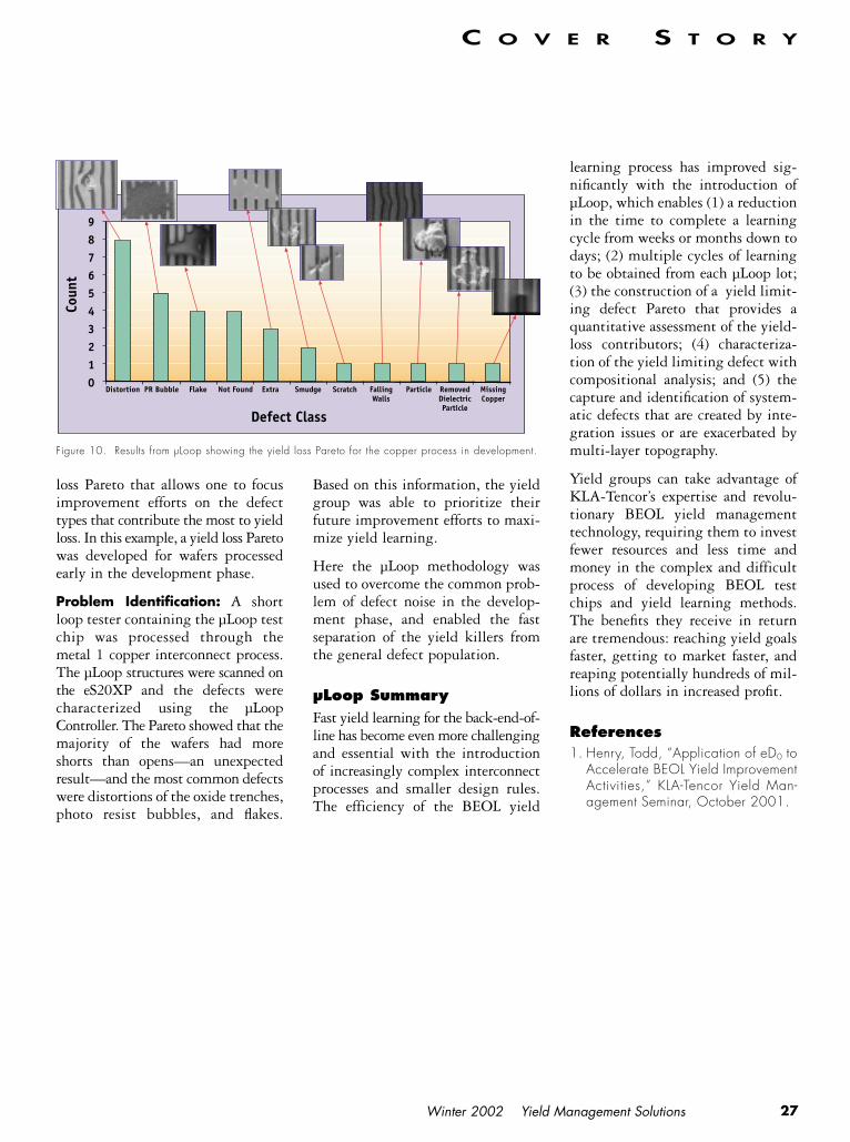
Case study 3: Early yield learningon a copper processIntroduction: Yield learning on newtechnologies is especially challengingdue to the large number of defectspresent on wafers as new processes arebeing developed. Attacking all of thedifferent defect types at the same timediffuses the available resources andresults in slow yield improvement.The key to success is to obtain a yield
Defe
ct D
ensi
ty (
cm-2
)
Outer edge spatial signature
Defect Class
Narrowing W Puddle Particle withExtra
Extra
Figure 9. Results from µLoop showing the narrowing space defect and signature.
C O V E R S T O R Y
27Winter 2002 Yield Management Solutions
loss Pareto that allows one to focusimprovement efforts on the defecttypes that contribute the most to yieldloss. In this example, a yield loss Paretowas developed for wafers processedearly in the development phase.
Problem Identification: A shortloop tester containing the µLoop testchip was processed through themetal 1 copper interconnect process.The µLoop structures were scanned onthe eS20XP and the defects werecharacterized using the µLoopController. The Pareto showed that themajority of the wafers had moreshorts than opens—an unexpectedresult—and the most common defectswere distortions of the oxide trenches,photo resist bubbles, and flakes.
Based on this information, the yieldgroup was able to prioritize theirfuture improvement efforts to maxi-mize yield learning.
Here the µLoop methodology wasused to overcome the common prob-lem of defect noise in the develop-ment phase, and enabled the fastseparation of the yield killers fromthe general defect population.
µLoop SummaryFast yield learning for the back-end-of-line has become even more challengingand essential with the introductionof increasingly complex interconnectprocesses and smaller design rules.The efficiency of the BEOL yield
learning process has improved sig-nificantly with the introduction ofµLoop, which enables (1) a reductionin the time to complete a learningcycle from weeks or months down todays; (2) multiple cycles of learningto be obtained from each µLoop lot;(3) the construction of a yield limit-ing defect Pareto that provides aquantitative assessment of the yield-loss contributors; (4) characteriza-tion of the yield limiting defect withcompositional analysis; and (5) thecapture and identification of system-atic defects that are created by inte-gration issues or are exacerbated bymulti-layer topography.
Yield groups can take advantage ofKLA-Tencor’s expertise and revolu-tionary BEOL yield managementtechnology, requiring them to investfewer resources and less time andmoney in the complex and difficultprocess of developing BEOL testchips and yield learning methods.The benefits they receive in returnare tremendous: reaching yield goalsfaster, getting to market faster, andreaping potentially hundreds of mil-lions of dollars in increased profit.
References1. Henry, Todd, “Application of eD0 to
Accelerate BEOL Yield ImprovementActivities,” KLA-Tencor Yield Man-agement Seminar, October 2001.
Coun
t
9876543210
Defect Class
Distortion PR Bubble Flake Not Found Extra Smudge Scratch FallingWalls
Particle RemovedDielectricParticle
MissingCopper
Figure 10. Results from µLoop showing the yield loss Pareto for the copper process in development.
C O V E R S T O R Y

in optimizing your manufacturing process. All strategically
formulated to enhance your bottom line. And put you on
the most efficient road to yield. For more information,
please visit us on the Web
at www.kla-tencor.com,
or call 1-800-450-5308.Accelerating Yield
©2001 KLA-Tencor Corporation
There are many paths to yield.
But these days, only the fastest route will do. That’s
why we focus relentlessly on shortening your journey.
With best-of-breed solutions designed to let process
control contribute directly to profitability. Yield
acceleration expertise that’s as deep as it is broad.
And industry neutrality, for unprecedented flexibility
YIELD