Embed Size (px)
Citation preview
Wireless Implantable Microsystems:High-Density Electronic Interfaces to theNervous System
K. D. WISE, FELLOW, IEEE, D. J. ANDERSON, J. F. HETKE, D. R. KIPKE, MEMBER, IEEE, AND
K. NAJAFI, FELLOW, IEEE
Invited Paper
This paper describes the development of a high-density electronicinterface to the central nervous system. Silicon micromachinedelectrode arrays now permit the long-term monitoring of neuralactivity in vivo as well as the insertion of electronic signalsinto neural networks at the cellular level. Efforts to understandand engineer the biology of the implant/tissue interface arealso underway. These electrode arrays are facilitating significantadvances in our understanding of the nervous system, and mergedwith on-chip circuitry, signal processing, microfluidics, and wirelessinterfaces, they are forming the basis for a family of neuralprostheses for the possible treatment of disorders such as blindness,deafness, paralysis, severe epilepsy, and Parkinson’s disease.
Keywords—Microelectrodes, microfluidics, micromachining,microsystems, nervous system, neural implants, sensors.
I. INTRODUCTION
Man has struggled to understand the nervous system anddevelop treatments for its disorders for centuries. BenjaminFranklin explored the use of electrical currents as an ap-proach to overcoming paralysis [1], but it was not until thelast century that investigations at the cellular level were re-ally possible. Today, both our understanding of the nervoussystem and our ability to treat a variety of its disorders usingneural prostheses appear ready to make dramatic progress asthe result of combining bioMEMS with microelectronics.
Manuscript received March 23, 2003; revised July 28, 2003. This workwas supported in part by the Neural Prosthesis Program of the National In-stitute of Neurological Disorders and Stroke, National Institutes of Health(NIH), in part by the NIH National Center for Research Resources, in partby the National Institute of Biomedical Imaging and Bioengineering, and inpart by the Engineering Research Centers Program, National Science Foun-dation under Award EEC-9 986 866.
The authors are with the Engineering Research Center for Wireless Inte-grated MicroSystems, University of Michigan, Ann Arbor, MI 48109-2122USA.
Digital Object Identifier 10.1109/JPROC.2003.820544
Beginning in the 1950s, the use of microelectrodes to-gether with electronic recording and signal processing beganto allow meaningful studies of the central nervous systemat the cellular level [2]. Gradually, a great deal was learnedabout the workings of single neurons. Serially moving sharp-ened wire electrodes in tissue also allowed considerable in-formation to be gained about the function of the nervoussystem at the circuit level, especially in sensory areas. How-ever, it was quickly clear that arrays of electrodes, and per-haps large arrays, would be needed to really understand thesignal processing performed in complex neural networks.Early experiments facilitated by gluing individual electrodestogether or using cutoff wire bundles [3], [4] to record si-multaneously from many points met with some success butwere limited in their geometries and reproducibility, causedconsiderable insertion damage, and tended to splay out intissue, making exact site placements uncertain. Nevertheless,they could be fabricated easily with available technology. Mi-crowire electrode arrays are still used extensively for bothacute and chronic extracellular recording [5]–[7].
In 1965, Prof. J. L. Moll at Stanford University, Stanford,CA, suggested that the lithographic techniques and siliconetching technology then being developed for beam-lead inte-grated circuits (ICs) [8] at Bell Telephone Laboratories mightbe used to produce electrode arrays capable of recordingfrom many points in tissue simultaneously and with no moredamage than a single metal microelectrode. Professor J. B.Angell led a project that soon demonstrated such electrodes[9]–[11]; however, at this point, the technologies availablefor silicon etching were not sufficiently precise to allow theprobes to be produced reproducibly with high yield. Theneeded technology was developed over the next two decadesas part of the more general development of integrated sen-sors and microelectromechanical systems (MEMS). During
0018-9219/04$20.00 © 2004 IEEE
76 PROCEEDINGS OF THE IEEE, VOL. 92, NO. 1, JANUARY 2004
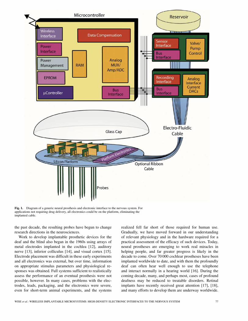
Fig. 1. Diagram of a generic neural prosthesis and electronic interface to the nervous system. Forapplications not requiring drug delivery, all electronics could be on the platform, eliminating theimplanted cable.
the past decade, the resulting probes have begun to changeresearch directions in the neurosciences.
Work to develop implantable prosthetic devices for thedeaf and the blind also began in the 1960s using arrays ofmetal electrodes implanted in the cochlea [12], auditorynerve [13], inferior colliculus [14], and visual cortex [15].Electrode placement was difficult in these early experimentsand all electronics was external, but over time, informationon appropriate stimulus parameters and physiological re-sponses was obtained. Full systems sufficient to realisticallyassess the performance of an eventual prosthesis were notpossible, however. In many cases, problems with the elec-trodes, leads, packaging, and the electronics were severe,even for short-term animal experiments, and the systems
realized fell far short of those required for human use.Gradually, we have moved forward in our understandingof relevant physiology and in the hardware required for apractical assessment of the efficacy of such devices. Today,neural prostheses are emerging to work real miracles inhelping people, and far greater progress is likely in thedecade to come. Over 70 000 cochlear prostheses have beenimplanted worldwide to date, and with them the profoundlydeaf can often hear well enough to use the telephoneand interact normally in a hearing world [16]. During thecoming decade, many, and perhaps most, cases of profounddeafness may be reduced to treatable disorders. Retinalimplants have recently received great attention [17], [18],and many efforts to develop them are underway worldwide.
WISE et al.: WIRELESS IMPLANTABLE MICROSYSTEMS: HIGH-DENSITY ELECTRONIC INTERFACES TO THE NERVOUS SYSTEM 77
Deep-brain electrodes for managing severe Parkinson’sdisease have proven remarkably effective [19], even thoughthe mechanisms by which they operate are not yet com-pletely understood. Devices for managing severe epilepsyare in development, and the first experiments aimed atcapturing motor control signals from the cortex to eventuallyrestore at least limited movement to quadriplegics have beenpromising [20]–[22].
All of these efforts to better understand the nervous systemand develop practical prostheses for its disorders depend onbuilding an electronic (and perhaps chemical) interface tothe cellular world. Fig. 1 shows one possible form for suchan interface, where a high-density three-dimensional (3-D)electrode array penetrates the tissue to monitor its electricalactivity (record), insert electrical signals (stimulate), or con-trol the local chemical environment (drug delivery). The in-dividual probe shanks supporting the recording, stimulating,and drug delivery sites should be small enough to be virtu-ally invisible to the tissue. The interface electronics is par-titioned here between the probes themselves, the platform,and in some cases, a remote electronics package. Excludingthe need for any chemical reservoir, the structure could beself-contained, remotely powered, monitored, and controlledusing a bidirectional RF telemetry link. While this systemcould take a number of physical forms, it is envisioned hereas a button-size implant with a diameter of a few millimetersand a height above the platform of no more than 1 mm. Thekey parts of any such system are the electrodes themselves,the interface electronics, the wireless link, and the packaging.This paper describes recent progress in each of these areas.
II. SILICON MICROMACHINED ELECTRODE ARRAYS
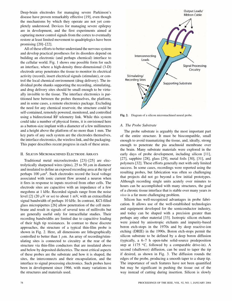
Traditional metal microelectrodes [23]–[25] are elec-trolytically sharpened wires (pins), 25 to 50 m in diameterand insulated to define an exposed recording area at the tip ofperhaps 100 m . Such electrodes record the local voltageassociated with ionic current flow around a neuron whenit fires in response to inputs received from other cells. Theelectrode sites are capacitive with an impedance of a fewmegohms at 1 kHz. Recorded signals range from the noiselevel [2] (20 V or so) to about 1 mV, with an extracellularsignal bandwidth of perhaps 10 kHz. In contrast, KCl-filledglass micropipettes [26] allow penetration of the cell mem-brane and result in signals of several tens of millivolts butare generally useful only for intracellular studies. Theirrecording bandwidths are limited due to capacitive loadingof their high tip resistances. In contrast to these discreteapproaches, the structure of a typical thin-film probe isshown in Fig. 2. Here, all dimensions are lithographicallycontrolled to better than 1 m. An array of recording/stim-ulating sites is connected to circuitry at the rear of thestructure via thin-film conductors that are insulated aboveand below by deposited dielectrics. The most critical aspectsof these probes are the substrate and how it is shaped, thesites, the interconnects and their encapsulation, and theinterface to signal processing electronics. Such probes havebeen in development since 1966, with many variations inthe structures and materials used.
Fig. 2. Diagram of a silicon micromachined neural probe.
A. The Probe Substrate
The probe substrate is arguably the most important partof the entire structure. It must be biocompatible, smallenough to avoid traumatizing the tissue, and, ideally, strongenough to penetrate the pia arachnoid membrane overthe brain. Many substrate materials were explored in theearly days of probe development, including silicon [11],[27], sapphire [28], glass [29], metal foils [30], [31], andpolymers [32]. These efforts generally met with only limitedsuccess. In some cases, recordings were reported using theresulting probes, but fabrication was often so challengingthat projects did not go beyond a few initial prototypes.Although recording single units acutely over minutes tohours can be accomplished with many structures, the goalof a chronic tissue interface that is stable over many years invivo is a far more challenging problem.
Silicon has well-recognized advantages in probe fabri-cation. It allows use of the well-established technologiesand equipment developed for the semiconductor industry,and today can be shaped with a precision greater thanperhaps any other material [33]. Isotropic silicon etchantswere joined by anisotropic etchants and impurity-basedboron etch-stops in the 1970s and by deep reactive-ionetching (DRIE) in the 1990s. Boron etch-stops permit thesilicon substrate to be defined by a deep boron diffusion(typically, a 6–7 h open-tube solid-source predepositionstep at 1175 C, followed by a comparable drive-in). Asecond (shallower) diffusion, can be used to taper the tipif desired, as shown in Fig. 3. The diffusion rounds theedges of the probe, producing a smooth taper to a sharp tip.The importance of such features have not been quantifiedbut may be significant in pushing the tissue out of theway instead of cutting during insertion. Silicon is slowly
78 PROCEEDINGS OF THE IEEE, VOL. 92, NO. 1, JANUARY 2004
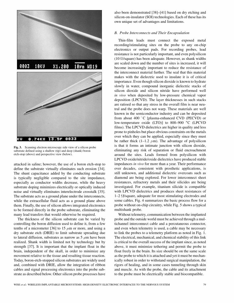
Fig. 3. Scanning electron microscopy side view of a silicon probesubstrate defined using a shallow (tip) and deep (shank) boronetch-stop (above) and perspective view (below).
attacked in saline; however, the use of a boron etch-stop todefine the substrate virtually eliminates such erosion [34].The shunt capacitance added by the conducting substrateis typically negligible compared to the site impedance,especially as conductor widths decrease, while the heavysubstrate doping minimizes electrically or optically inducednoise and virtually eliminates interelectrode crosstalk [35].The substrate acts as a ground plane under the interconnects,while the extracellular fluid acts as a ground plane abovethem. Finally, the use of silicon allows integrated electronicsto be formed directly in the probe substrate, eliminating themany lead transfers that would otherwise be required.
The thickness of the silicon substrate can be varied bycontrolling the boron diffusion used to define it, from a fewtenths of a micrometer [36] to 15 m or more, and using adry substrate etch (DRIE) to limit substrate spreading dueto lateral diffusion, substrates as narrow as 5 m have beenrealized. Shank width is limited not by technology but bystrength [37]. It is important that the implant float in thebrain, independent of the skull, in order to minimize anymovement relative to the tissue and resulting tissue reaction.Today, boron-etch-stopped silicon substrates are widely usedand, combined with DRIE, allow the integration of ribboncables and signal processing electronics into the probe sub-strate as described below. Other silicon probe processes have
also been demonstrated [38]–[41] based on dry etching andsilicon-on-insulator (SOI) technologies. Each of these has itsown unique set of advantages and limitations.
B. Probe Interconnects and Their Encapsulation
Thin-film leads must connect the exposed metalrecording/stimulating sites on the probe to any on-chipelectronics or output pads. For recording probes, leadresistance is not particularly important, and even polysilicon(10 /square) has been adequate. However, as shank widthsare scaled down and the number of sites is increased, it willbecome increasingly important to reduce the resistance ofthe interconnect material further. The seal that this materialmakes with the dielectric used to insulate it is of criticalimportance. Even though silicon dioxide is known to hydrateslowly in water, compound inorganic dielectric stacks ofsilicon dioxide and silicon nitride have performed wellin vivo when deposited by low-pressure chemical vapordeposition (LPCVD). The layer thicknesses in such stacksare ratioed so that any stress in the overall film is near neu-tral and the probe does not warp. These materials are wellknown in the semiconductor industry and can be depositedfrom about 400 C [plasma-enhanced CVD (PECVD) orlow-temperature oxide (LTO)] to 800–900 C (LPCVDfilms). The LPCVD dielectrics are higher in quality and lessprone to pinholes but place obvious constraints on the metalsover which they can be applied, especially since they mustbe rather thick (1–1.2 m). The advantage of polysiliconis that it forms an intimate junction with silicon dioxide,eliminating any risk of separation or fluid encroachmentaround the sites. Leads formed from polysilicon withLPCVD oxide/nitride/oxide dielectrics have produced stableimpedances in vivo for more than a year. Their performanceover decades, consistent with prosthetic applications, isstill unknown, and additional dielectric overcoats such asdiamond are being explored. For lower interconnect sheetresistances, refractory metals and their silicides are beinginvestigated. For example, titanium silicide is compatiblewith LPCVD dielectrics and produces sheet resistances of1–2 /square, adequate for most stimulating electrodes andsome cables. Fig. 4 summarizes the basic process flow for aprobe without on-chip circuitry, while Fig. 5 shows a typicalmultishank probe.
Without telemetry, communication between the implantedprobe and the outside world must be achieved through a mul-tichannel interconnect cable and a percutaneous connector,and even when telemetry is used, a cable may be necessaryto link the probes to a telemetry platform as noted in Fig. 1.The electrical, mechanical, and chemical stability of this linkis critical to the overall success of the implant since, as notedabove, it must minimize tethering and permit the probe tofloat freely in the brain. Its size should be on the same scaleas the probe to which it is attached and yet it must be mechan-ically robust in order to withstand surgical manipulation, therigors of healing, and in some cases tunneling through skinand muscle. As with the probe, the cable and its attachmentto the probe must be electrically stable and biocompatible.
WISE et al.: WIRELESS IMPLANTABLE MICROSYSTEMS: HIGH-DENSITY ELECTRONIC INTERFACES TO THE NERVOUS SYSTEM 79
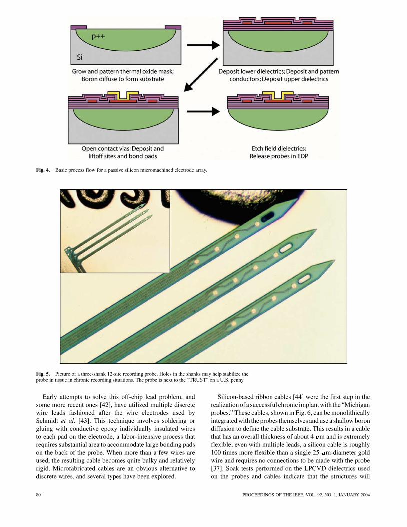
Fig. 4. Basic process flow for a passive silicon micromachined electrode array.
Fig. 5. Picture of a three-shank 12-site recording probe. Holes in the shanks may help stabilize theprobe in tissue in chronic recording situations. The probe is next to the “TRUST” on a U.S. penny.
Early attempts to solve this off-chip lead problem, andsome more recent ones [42], have utilized multiple discretewire leads fashioned after the wire electrodes used bySchmidt et al. [43]. This technique involves soldering orgluing with conductive epoxy individually insulated wiresto each pad on the electrode, a labor-intensive process thatrequires substantial area to accommodate large bonding padson the back of the probe. When more than a few wires areused, the resulting cable becomes quite bulky and relativelyrigid. Microfabricated cables are an obvious alternative todiscrete wires, and several types have been explored.
Silicon-based ribbon cables [44] were the first step in therealization of a successful chronic implant with the “Michiganprobes.” These cables, shown in Fig. 6, can be monolithicallyintegrated with the probes themselves and use a shallow borondiffusion to define the cable substrate. This results in a cablethat has an overall thickness of about 4 m and is extremelyflexible; even with multiple leads, a silicon cable is roughly100 times more flexible than a single 25- m-diameter goldwire and requires no connections to be made with the probe[37]. Soak tests performed on the LPCVD dielectrics usedon the probes and cables indicate that the structures will
80 PROCEEDINGS OF THE IEEE, VOL. 92, NO. 1, JANUARY 2004
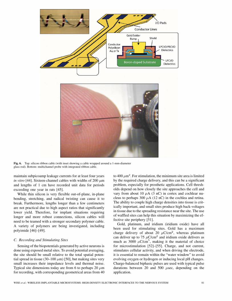
Fig. 6. Top: silicon ribbon cable (with inset showing a cable wrapped around a 1-mm-diameterglass rod). Bottom: multichannel probe with integrated ribbon cable.
maintain subpicoamp leakage currents for at least four yearsin vitro [44]. Sixteen-channel cables with widths of 200 mand lengths of 1 cm have recorded unit data for periodsexceeding one year in rats [45].
While thin silicon is very flexible out-of-plane, in-planebending, stretching, and radical twisting can cause it tobreak. Furthermore, lengths longer than a few centimetersare not practical due to high aspect ratios that significantlylower yield. Therefore, for implant situations requiringlonger and more robust connections, silicon cables willneed to be teamed with a stronger secondary polymer cable.A variety of polymers are being investigated, includingpolyimide [46]–[49].
C. Recording and Stimulating Sites
Sensing of the biopotentials generated by active neurons isdone using exposed metal sites. To avoid potential averaging,the site should be small relative to the total spatial poten-tial spread in tissue (30–100 m) [50], but making sites verysmall increases their impedance levels and thermal noise.Typical site dimensions today are from 6 to perhaps 20 mfor recording, with corresponding geometrical areas from 40
to 400 m . For stimulation, the minimum site area is limitedby the required charge delivery, and this can be a significantproblem, especially for prosthetic applications. Cell thresh-olds depend on how closely the site approaches the cell andvary from about 10 A (3 nC) in cortex and cochlear nu-cleus to perhaps 300 A (12 nC) in the cochlea and retina.The ability to couple high charge densities into tissue is crit-ically important, and small sites produce high back-voltagesin tissue due to the spreading resistance near the site. The useof waffled sites can help this situation by maximizing the ef-fective site periphery [51].
Gold, platinum, and iridium (iridium oxide) have allbeen used for stimulating sites. Gold has a maximumcharge delivery of about 20 C/cm , whereas platinumcan deliver up to 75 C/cm and iridium oxide delivers asmuch as 3000 C/cm , making it the material of choicefor microstimulation [52]–[55]. Charge, and not current,stimulates cellular activity, and when driving the electrode,it is essential to remain within the “water window” to avoidevolving oxygen or hydrogen or inducing local pH changes.Charge-balanced biphasic pulses are used with typical pulsedurations between 20 and 500 sec, depending on theapplication.
WISE et al.: WIRELESS IMPLANTABLE MICROSYSTEMS: HIGH-DENSITY ELECTRONIC INTERFACES TO THE NERVOUS SYSTEM 81
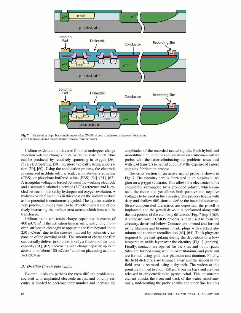
Fig. 7. Fabrication of probes containing on-chip CMOS circuitry: etch-stop and p-well formation;circuit fabrication and encapsulation; release from the wafer.
Iridium oxide is a multilayered film that undergoes chargeinjection valence changes in its oxidation state. Such filmscan be produced by reactively sputtering in oxygen [56],[57], electroplating [58], or, more typically, using anodiza-tion [59], [60]. Using the anodization process, the electrodeis immersed in dilute sulfuric acid, carbonate-buffered saline(CBS), or phosphate-buffered saline (PBS) [54], [61], [62].A triangular voltage is forced between the working electrodeand a saturated calomel electrode (SCE) reference and is cy-cled between limits set by hydrogen and oxygen evolution. Ahydrous oxide film builds in thickness on the iridium surfaceas the potential is continuously cycled. The hydrous oxide isvery porous, allowing water to be absorbed into it and effec-tively increasing the surface area across which ions can betransferred.
Iridium oxide can attain charge capacities in excess of400 mC/cm if the activation time is sufficiently long; how-ever, surface cracks begin to appear in the film beyond about250 mC/cm due to the stresses induced by volumetric ex-pansion of the growing oxide. The amount of charge the filmcan actually deliver to solution is only a fraction of the totalcapacity [61], [62], increasing with charge capacity up to anactivation of about 100 mC/cm and then plateauing at about1–3 mC/cm .
D. On-Chip Circuit Fabrication
External leads are perhaps the most difficult problem as-sociated with implanted electrode arrays, and on-chip cir-cuitry is needed to decrease their number and increase the
amplitudes of the recorded neural signals. Both hybrid andmonolithic circuit options are available on a silicon-substrateprobe, with the latter eliminating the problems associatedwith lead transfers to hybrid circuitry at the expense of a morecomplex fabrication process.
The cross section of an active neural probe is shown inFig. 7. The circuitry here is fabricated in an n-epitaxial re-gion on a p-type substrate. This allows the electronics to becompletely surrounded by a grounded p-layer, which con-tacts the tissue and yet allows both positive and negativevoltages to be used in the circuitry. The process begins withdeep and shallow diffusions to define the intended substrate.Stress-compensated dielectrics are deposited, the p-well isimplanted, and the p-well drive-in is performed along withthe last portion of the etch-stop diffusions [Fig. 7 (top)] [63].A standard p-well CMOS process is then used to form thecircuitry, described below. Contacts are opened and formedusing titanium and titanium nitride plugs with stacked alu-minum and titanium metallization [63], [64]. Thick plugs arerequired to prevent spiking during the deposition of a low-temperature oxide layer over the circuitry [Fig. 7 (center)].Finally, contacts are opened for the sites and output pads.Sites are formed using iridium over titanium, and pads andare formed using gold over platinum and titanium. Finally,the field dielectrics are trimmed away and the silicon in thefield area is recessed using a dry etch. The wafers at thispoint are thinned to about 150 m from the back and are thenreleased in ethylenediamine pyrocatechol. This anisotropicetchant attacks the front and back of the wafer simultane-ously, undercutting the probe shanks and other fine features
82 PROCEEDINGS OF THE IEEE, VOL. 92, NO. 1, JANUARY 2004
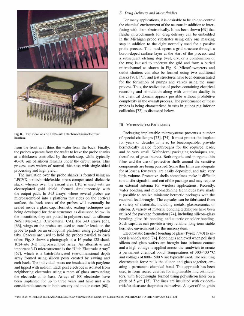
Fig. 8. Two views of a 3-D 1024-site 128-channel neuroelectronicinterface.
from the front as it thins the wafer from the back. Finally,the probes separate from the wafer to leave the probe shanksat a thickness controlled by the etch-stop, while typically40–50 m of silicon remains under the circuit areas. Thisprocess uses wafers of normal thickness with single-sidedprocessing and high yield.
The insulation over the probe shanks is formed using anLPCVD oxide/nitride/oxide stress-compensated dielectricstack, whereas over the circuit area LTO is used with anelectroplated gold shield, formed simultaneously withthe output pads. In 3-D arrays, where several probes aremicroassembled into a platform that rides on the corticalsurface, the back areas of the probes will eventually besealed inside a glass cap. Hermetic sealing techniques arebeing developed for these structures as discussed below; inthe meantime, they are potted in polymers such as siliconeNuSil Med-4211 (Carpenteria, CA). For 3-D arrays [65],[66], wings on the probes are used to transfer leads on theprobe to pads on an orthogonal platform using gold-platedtabs. Spacers are used to hold the probes parallel to eachother. Fig. 8 shows a photograph of a 16-probe 128-shank1024-site 3-D microassembled array. An alternative andimportant 3-D microstructure is the “Utah Electrode Array”[67], which is a batch-fabricated two-dimensional deptharray formed using silicon posts created by sawing andetch-back. The individual posts are insulated with paryleneand tipped with iridium. Each post electrode is isolated fromneighboring electrodes using a mote of glass surroundingthe electrode at its base. Arrays of 100 electrodes havebeen implanted for up to three years and have met withconsiderable success in both sensory and motor cortex [68].
E. Drug Delivery and Microfluidics
For many applications, it is desirable to be able to controlthe chemical environment of the neurons in addition to inter-facing with them electronically. It has been shown [69] thatfluidic microchannels for drug delivery can be embeddedin the Michigan probe substrates using only one maskingstep in addition to the eight normally used for a passiveprobe process. This mask opens a grid structure through aboron-doped surface layer at the start of the process, anda subsequent etching step (wet, dry, or a combination ofthe two) is used to undercut the grid and form a buriedmicrochannel as shown in Fig. 9. Microflowmeters andoutlet shutters can also be formed using two additionalmasks [70], [71], and test structures have been demonstratedfor the formation of pumps and valves using the sameprocess. Thus, the realization of probes containing electricalrecording and stimulation along with complete duality inthe chemical domain appears possible without prohibitivecomplexity in the overall process. The performance of theseprobes is being characterized in vivo in guinea pig inferiorcolliculus [72] as discussed below.
III. MICROSYSTEM PACKAGING
Packaging implantable microsystems presents a numberof special challenges [73], [74]. It must protect the implantfor years or decades in vivo, be biocompatible, providehermetically sealed feedthroughs for the required leads,and be very small. Wafer-level packaging techniques are,therefore, of great interest. Both organic and inorganic thinfilms and the use of protective shells around the sensitivecomponents are being pursued. Some thin films are adequatefor at least a few years, are easily deposited, and take verylittle volume. Protective shells sometimes make it difficultto transfer signals in and out of the package and may requirean external antenna for wireless applications. Recently,wafer bonding and micromachining techniques have madeit possible to realize miniature hermetic packages with therequired feedthroughs. The capsules can be fabricated froma variety of materials, including metals, glass/ceramic, orsilicon. A variety of material bonding techniques have beenutilized for package formation [74], including silicon–glassbonding, glass frit bonding, and eutectic or solder bonding.Such capsules can provide a very reliable, long-term stablehermetic environment for the microsystem.
Electrostatic (anodic) bonding of glass (Pyrex 7740) to sil-icon is widely used [74]. Bonding is achieved when polishedsilicon and glass wafers are brought into intimate contactand a high voltage is applied across the sandwich to createa permanent chemical bond. Temperatures of 300–400 Cand voltages of 800–1500 V are typically used. The resultingelectrostatic force pulls the silicon and glass together, cre-ating a permanent chemical bond. This approach has beenused to form sealed cavities for implantable microstimula-tors, with feedthroughs formed using polysilicon lines on apitch of 5 m [75]. The lines are insulated with oxide/ni-tride/oxide as are the probes themselves. A layer of fine-grain
WISE et al.: WIRELESS IMPLANTABLE MICROSYSTEMS: HIGH-DENSITY ELECTRONIC INTERFACES TO THE NERVOUS SYSTEM 83
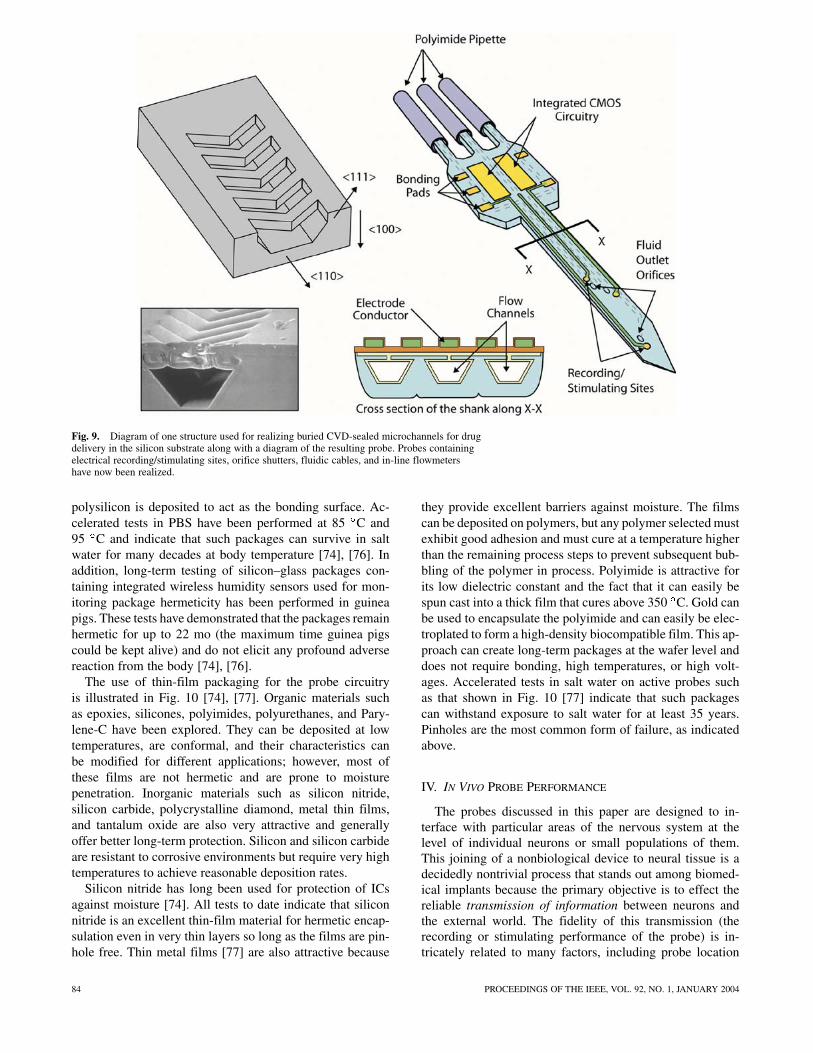
Fig. 9. Diagram of one structure used for realizing buried CVD-sealed microchannels for drugdelivery in the silicon substrate along with a diagram of the resulting probe. Probes containingelectrical recording/stimulating sites, orifice shutters, fluidic cables, and in-line flowmetershave now been realized.
polysilicon is deposited to act as the bonding surface. Ac-celerated tests in PBS have been performed at 85 C and95 C and indicate that such packages can survive in saltwater for many decades at body temperature [74], [76]. Inaddition, long-term testing of silicon–glass packages con-taining integrated wireless humidity sensors used for mon-itoring package hermeticity has been performed in guineapigs. These tests have demonstrated that the packages remainhermetic for up to 22 mo (the maximum time guinea pigscould be kept alive) and do not elicit any profound adversereaction from the body [74], [76].
The use of thin-film packaging for the probe circuitryis illustrated in Fig. 10 [74], [77]. Organic materials suchas epoxies, silicones, polyimides, polyurethanes, and Pary-lene-C have been explored. They can be deposited at lowtemperatures, are conformal, and their characteristics canbe modified for different applications; however, most ofthese films are not hermetic and are prone to moisturepenetration. Inorganic materials such as silicon nitride,silicon carbide, polycrystalline diamond, metal thin films,and tantalum oxide are also very attractive and generallyoffer better long-term protection. Silicon and silicon carbideare resistant to corrosive environments but require very hightemperatures to achieve reasonable deposition rates.
Silicon nitride has long been used for protection of ICsagainst moisture [74]. All tests to date indicate that siliconnitride is an excellent thin-film material for hermetic encap-sulation even in very thin layers so long as the films are pin-hole free. Thin metal films [77] are also attractive because
they provide excellent barriers against moisture. The filmscan be deposited on polymers, but any polymer selected mustexhibit good adhesion and must cure at a temperature higherthan the remaining process steps to prevent subsequent bub-bling of the polymer in process. Polyimide is attractive forits low dielectric constant and the fact that it can easily bespun cast into a thick film that cures above 350 C. Gold canbe used to encapsulate the polyimide and can easily be elec-troplated to form a high-density biocompatible film. This ap-proach can create long-term packages at the wafer level anddoes not require bonding, high temperatures, or high volt-ages. Accelerated tests in salt water on active probes suchas that shown in Fig. 10 [77] indicate that such packagescan withstand exposure to salt water for at least 35 years.Pinholes are the most common form of failure, as indicatedabove.
IV. IN VIVO PROBE PERFORMANCE
The probes discussed in this paper are designed to in-terface with particular areas of the nervous system at thelevel of individual neurons or small populations of them.This joining of a nonbiological device to neural tissue is adecidedly nontrivial process that stands out among biomed-ical implants because the primary objective is to effect thereliable transmission of information between neurons andthe external world. The fidelity of this transmission (therecording or stimulating performance of the probe) is in-tricately related to many factors, including probe location
84 PROCEEDINGS OF THE IEEE, VOL. 92, NO. 1, JANUARY 2004
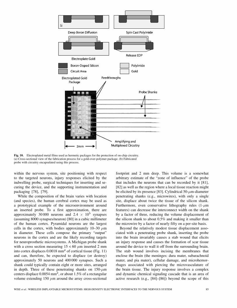
Fig. 10. Electroplated metal films used as hermetic packages for the protection of on-chip circuitry.(a) Cross-sectional view of the fabrication process for a gold-over-polymer package. (b) Fabricatedprobe with circuitry encapsulated using this process.
within the nervous system, site positioning with respectto the targeted neurons, injury responses elicited by theindwelling probe, surgical techniques for inserting and se-curing the device, and the supporting instrumentation andpackaging [78], [79].
While the composition of the brain varies with location(and species), the human cerebral cortex may be used asa prototypical example of the microenvironment aroundan inserted probe. To a first approximation, there areapproximately 30 000 neurons and 2.4 10 synapses(assuming 8000 synapses/neuron) [80] in a cubic millimeterof the human cortex. Pyramidal neurons are the largestcells in the cortex, with bodies approximately 10–30 min diameter. These cells compose the primary “output”neurons in the cortex and are the likely recording targetsfor neuroprosthetic microsystems. A Michigan probe shankwith a cross section measuring 15 60 m inserted 2 mminto cortex displaces 0.0018 mm of cortical tissue (Fig. 11)and can, therefore, be expected to displace (or destroy)approximately 50 neurons and 400 000 synapses. Such ashank could typically contain eight or more sites, arrangedin depth. Three of these penetrating shanks on 150- mcenters displace 0.0054 mm , or about 1.5% of a rectangularvolume extending 150 m around the array cross-sectional
footprint and 2 mm deep. This volume is a somewhatarbitrary estimate of the “zone of influence” of the probethat includes the neurons that can be recorded by it [81],[82] as well as the region where a local tissue reaction mightbe elicited by its presence [83]. Cylindrical 50- m-diameterpenetrating shanks (e.g., microwires), with only a singlesite, displace about twice the tissue of the silicon shank.Furthermore, even conservative lithography rules (1- mfeatures) can decrease the interconnect width on the shankby a factor of three, reducing the volume displacement ofthe silicon shank to about 0.5% and making it smaller thanthe microwire by a factor of nearly fifty on a per-site basis.
Beyond the relatively modest tissue displacement asso-ciated with a penetrating probe shank, inserting the probeinto the brain invariably causes a stab wound that elicitsan injury response and causes the formation of scar tissuearound the device to wall it off from the surrounding brain.The stab wound involves incising the membranes thatenclose the brain (the meninges: dura mater, subarachnoidmater, and pia mater), cellular damage, and microhemor-rhages associated with piercing the microvasculature ofthe brain tissue. The injury response involves a complexand dynamic chemical signaling cascade that is an area ofactive research (e.g., [84]–[86]) beyond the scope of this
WISE et al.: WIRELESS IMPLANTABLE MICROSYSTEMS: HIGH-DENSITY ELECTRONIC INTERFACES TO THE NERVOUS SYSTEM 85
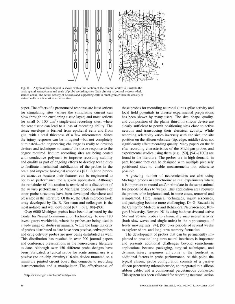
Fig. 11. A typical probe layout is shown with a thin section of the cerebral cortex to illustrate thebasic spatial arrangement and scale of probe recording sites (dark circles) to cortical neurons (darkstained cells). The actual density of neurons and supporting cells is much greater than the density ofstained cells in this cortical cross section.
paper. The effects of a pronounced response are least seriousfor stimulating sites (where the stimulating current canblow through the enveloping tissue layer) and most seriousfor small (< 100 m ) single-unit recording sites, wherethe scar tissue can lead to a loss of recording ability. Thetissue envelope is formed from epithelial cells and fromglia, with a total thickness of a few micrometers. Sincethe injury response can be mitigated—but not completelyeliminated—the engineering challenge is really to developdevices and techniques to control the tissue response to thedegree required. Iridium recording sites are being coatedwith conductive polymers to improve recording stabilityand quality as part of ongoing efforts to develop techniquesto facilitate mechanical stabilization of the probes in thebrain and improve biological responses [87]. Silicon probesare attractive because their features can be engineered tooptimize performance for a given application. Althoughthe remainder of this section is restricted to a discussion ofthe in vivo performance of Michigan probes, a number ofother probe structures have been developed elsewhere andpresented in the literature. Of these, the Utah microelectrodearray developed by Dr. R. Normann and colleagues is themost notable and well developed [67], [68], [88]–[93].
Over 6000 Michigan probes have been distributed by theCenter for Neural Communication Technology1 to over 180investigators worldwide, where the probes are being used ina wide range of studies in animals. While the large majorityof probes distributed to date have been passive, active probesand drug delivery probes are now being distributed as well.This distribution has resulted in over 200 journal papersand conference presentations in the neuroscience literatureto date. Although over 150 different probe designs havebeen fabricated, a typical probe for acute animal use is apassive (no on-chip circuitry) 16-site device mounted on aminiature printed circuit board that connects to recordinginstrumentation and a manipulator. The effectiveness of
1http://www.engin.umich.edu/facility/cnct/
these probes for recording neuronal (unit) spike activity andlocal field potentials in diverse experimental preparationshas been shown by many users. The size, shape, quality,and composition of the planar thin-film silicon device areclearly sufficient to permit positioning sites close to activeneurons and transducing their electrical activity. Whilerecording selectivity varies inversely with site size, the siteposition on the silicon substrate (tip, edge, middle) does notsignificantly affect recording quality. Many papers on the invivo recording characteristics of the Michigan probes andexperimental studies using them (e.g., [50], [94]–[100]) arefound in the literature. The probes are in high demand, inpart, because they can be designed with multiple preciselypositioned sites to enable measurements not otherwisepossible.
A growing number of neuroscientists are also usingMichigan probes in semichronic animal experiments whereit is important to record and/or stimulate in the same animalfor periods of days to weeks. This application area requiresthe probes to be implanted and, in some cases, removed andreimplanted. Here, surgical techniques, injury responses,and packaging become more challenging. Dr. G. Buzsaki inthe Center for Molecular and Behavioral Neuroscience, Rut-gers University, Newark, NJ, is using both passive and active64- and 96-site probes to chronically map neural activity(both slow-waves and single units) in the hippocampus offreely moving rats [94], [95] over periods of several weeksto explore short- and long-term memory formation.
The development of probes that can be permanently im-planted to provide long-term neural interfaces is importantand presents additional challenges beyond semichronicapplications because packaging, surgical techniques, anddynamic injury responses all come to the forefront asadditional factors in probe performance. At this point, thetypical chronic probe configuration consists of a passivesilicon penetrating microelectrode, an integrated thin siliconribbon cable, and a commercial percutaneous connector.This system has been validated for recording neuronal action
86 PROCEEDINGS OF THE IEEE, VOL. 92, NO. 1, JANUARY 2004
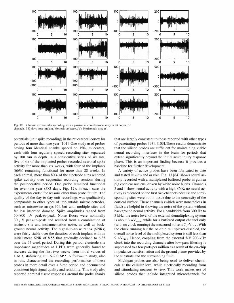
Fig. 12. Chronic extracellular recording with a passive silicon electrode array in rat cortex: 16channels, 383 days post implant. Vertical: voltage (�V); Horizontal: time (s).
potentials (unit spike recording) in the rat cerebral cortex forperiods of more than one year [101]. One study used probeshaving four identical shanks spaced on 150- m centers,each with four regularly spaced recording sites separatedby 100 m in depth. In a consecutive series of six rats,five of six of the implanted probes recorded neuronal spikeactivity for more than six weeks, with four of the implants(66%) remaining functional for more than 28 weeks. Ineach animal, more than 80% of the electrode sites recordedspike activity over sequential recording sessions duringthe postoperative period. One probe remained functionalfor over one year (383 days, Fig. 12); in each case theexperiments ended for reasons other than probe failure. Thequality of the day-to-day unit recordings was qualitativelycomparable to other types of implantable microelectrodes,such as microwire arrays [6], but with multiple sites andfar less insertion damage. Spike amplitudes ranged from50–800 V peak-to-peak. Noise floors were nominally30 V peak-to-peak and resulted from a combination ofintrinsic site and instrumentation noise, as well as back-ground neural activity. The signal-to-noise ratios (SNRs)were fairly stable over the duration of each implant with aninitial mean SNR of 8.55 that gradually declined to 6.35over the 54-week period. During this period, electrode siteimpedance magnitudes at 1 kHz were generally found toincrease during the first two weeks from initial values of1 M , stabilizing at 1.6–2.0 M . A follow-up study, alsoin rats, characterized the recording performance of theseprobes in more detail over a 3-mo period and documentedconsistent high signal quality and reliability. This study alsoreported nominal tissue responses around the probe shanks
that are largely consistent to those reported with other typesof penetrating probes [93], [103].These results demonstratethat the silicon probes are sufficient for maintaining viableneural recording interfaces in the brain for periods thatextend significantly beyond the initial acute injury responsephase. This is an important finding because it provides abaseline for further development.
A variety of active probes have been fabricated to dateand tested in vitro and in vivo. Fig. 13 [64] shows neural ac-tivity recorded with a multiplexed buffered probe in guineapig cochlear nucleus, driven by white noise bursts. Channels3 and 4 show neural activity with a high SNR; no neural ac-tivity is recorded on the first two channels because the corre-sponding sites were not in tissue due to the convexity of thecortical surface. These channels (which were nonetheless influid) are helpful in showing the noise of the system withoutbackground neural activity. For a bandwidth from 300 Hz to3 kHz, the noise level of the external demultiplexing systemis about 3 V , while for a buffered output channel only(with no clock running) the measured noise is 7 V . Withthe clock running but the on-chip multiplexer disabled, theoverall noise level of the multiplexed system is still less than9 V . Hence, coupling from the external 5-V 200-kHzclock into the recording channels after low-pass filtering issuppressed to a few parts per million as a result of the on-chipimpedance transformation and the ground planes provided bythe substrate and the surrounding fluid.
Michigan probes are also being used to deliver chemi-cals at the cellular level while electrically recording fromand stimulating neurons in vivo. This work makes use ofsilicon probes that include integrated microchannels for
WISE et al.: WIRELESS IMPLANTABLE MICROSYSTEMS: HIGH-DENSITY ELECTRONIC INTERFACES TO THE NERVOUS SYSTEM 87
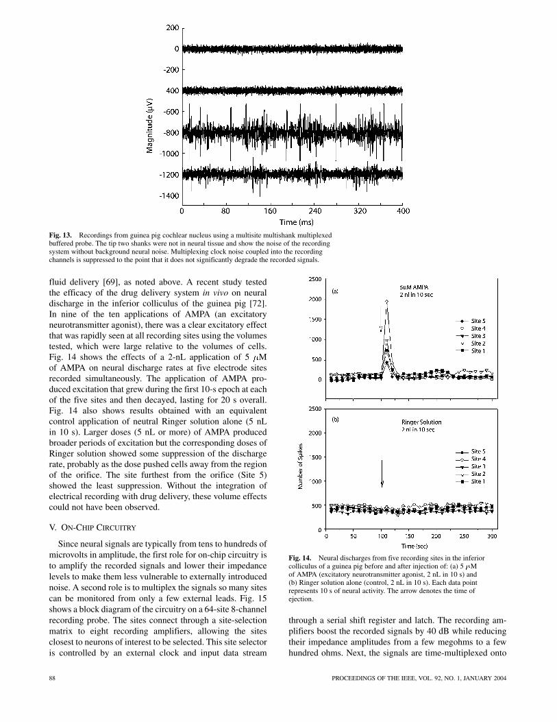
Fig. 13. Recordings from guinea pig cochlear nucleus using a multisite multishank multiplexedbuffered probe. The tip two shanks were not in neural tissue and show the noise of the recordingsystem without background neural noise. Multiplexing clock noise coupled into the recordingchannels is suppressed to the point that it does not significantly degrade the recorded signals.
fluid delivery [69], as noted above. A recent study testedthe efficacy of the drug delivery system in vivo on neuraldischarge in the inferior colliculus of the guinea pig [72].In nine of the ten applications of AMPA (an excitatoryneurotransmitter agonist), there was a clear excitatory effectthat was rapidly seen at all recording sites using the volumestested, which were large relative to the volumes of cells.Fig. 14 shows the effects of a 2-nL application of 5 Mof AMPA on neural discharge rates at five electrode sitesrecorded simultaneously. The application of AMPA pro-duced excitation that grew during the first 10-s epoch at eachof the five sites and then decayed, lasting for 20 s overall.Fig. 14 also shows results obtained with an equivalentcontrol application of neutral Ringer solution alone (5 nLin 10 s). Larger doses (5 nL or more) of AMPA producedbroader periods of excitation but the corresponding doses ofRinger solution showed some suppression of the dischargerate, probably as the dose pushed cells away from the regionof the orifice. The site furthest from the orifice (Site 5)showed the least suppression. Without the integration ofelectrical recording with drug delivery, these volume effectscould not have been observed.
V. ON-CHIP CIRCUITRY
Since neural signals are typically from tens to hundreds ofmicrovolts in amplitude, the first role for on-chip circuitry isto amplify the recorded signals and lower their impedancelevels to make them less vulnerable to externally introducednoise. A second role is to multiplex the signals so many sitescan be monitored from only a few external leads. Fig. 15shows a block diagram of the circuitry on a 64-site 8-channelrecording probe. The sites connect through a site-selectionmatrix to eight recording amplifiers, allowing the sitesclosest to neurons of interest to be selected. This site selectoris controlled by an external clock and input data stream
Fig. 14. Neural discharges from five recording sites in the inferiorcolliculus of a guinea pig before and after injection of: (a) 5 �Mof AMPA (excitatory neurotransmitter agonist, 2 nL in 10 s) and(b) Ringer solution alone (control, 2 nL in 10 s). Each data pointrepresents 10 s of neural activity. The arrow denotes the time ofejection.
through a serial shift register and latch. The recording am-plifiers boost the recorded signals by 40 dB while reducingtheir impedance amplitudes from a few megohms to a fewhundred ohms. Next, the signals are time-multiplexed onto
88 PROCEEDINGS OF THE IEEE, VOL. 92, NO. 1, JANUARY 2004
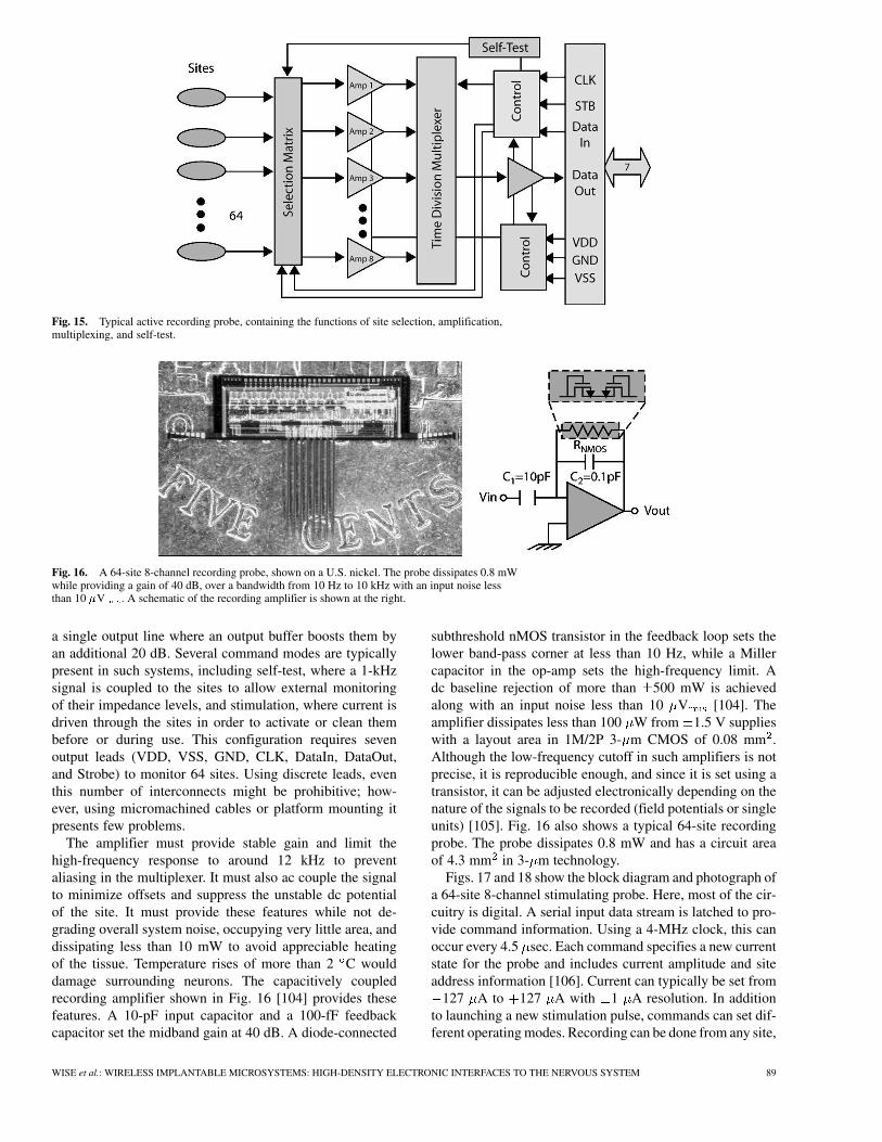
Fig. 15. Typical active recording probe, containing the functions of site selection, amplification,multiplexing, and self-test.
Fig. 16. A 64-site 8-channel recording probe, shown on a U.S. nickel. The probe dissipates 0.8 mWwhile providing a gain of 40 dB, over a bandwidth from 10 Hz to 10 kHz with an input noise lessthan 10 �V . A schematic of the recording amplifier is shown at the right.
a single output line where an output buffer boosts them byan additional 20 dB. Several command modes are typicallypresent in such systems, including self-test, where a 1-kHzsignal is coupled to the sites to allow external monitoringof their impedance levels, and stimulation, where current isdriven through the sites in order to activate or clean thembefore or during use. This configuration requires sevenoutput leads (VDD, VSS, GND, CLK, DataIn, DataOut,and Strobe) to monitor 64 sites. Using discrete leads, eventhis number of interconnects might be prohibitive; how-ever, using micromachined cables or platform mounting itpresents few problems.
The amplifier must provide stable gain and limit thehigh-frequency response to around 12 kHz to preventaliasing in the multiplexer. It must also ac couple the signalto minimize offsets and suppress the unstable dc potentialof the site. It must provide these features while not de-grading overall system noise, occupying very little area, anddissipating less than 10 mW to avoid appreciable heatingof the tissue. Temperature rises of more than 2 C woulddamage surrounding neurons. The capacitively coupledrecording amplifier shown in Fig. 16 [104] provides thesefeatures. A 10-pF input capacitor and a 100-fF feedbackcapacitor set the midband gain at 40 dB. A diode-connected
subthreshold nMOS transistor in the feedback loop sets thelower band-pass corner at less than 10 Hz, while a Millercapacitor in the op-amp sets the high-frequency limit. Adc baseline rejection of more than 500 mW is achievedalong with an input noise less than 10 V [104]. Theamplifier dissipates less than 100 W from 1.5 V supplieswith a layout area in 1M/2P 3- m CMOS of 0.08 mm .Although the low-frequency cutoff in such amplifiers is notprecise, it is reproducible enough, and since it is set using atransistor, it can be adjusted electronically depending on thenature of the signals to be recorded (field potentials or singleunits) [105]. Fig. 16 also shows a typical 64-site recordingprobe. The probe dissipates 0.8 mW and has a circuit areaof 4.3 mm in 3- m technology.
Figs. 17 and 18 show the block diagram and photograph ofa 64-site 8-channel stimulating probe. Here, most of the cir-cuitry is digital. A serial input data stream is latched to pro-vide command information. Using a 4-MHz clock, this canoccur every 4.5 sec. Each command specifies a new currentstate for the probe and includes current amplitude and siteaddress information [106]. Current can typically be set from
127 A to 127 A with 1 A resolution. In additionto launching a new stimulation pulse, commands can set dif-ferent operating modes. Recording can be done from any site,
WISE et al.: WIRELESS IMPLANTABLE MICROSYSTEMS: HIGH-DENSITY ELECTRONIC INTERFACES TO THE NERVOUS SYSTEM 89
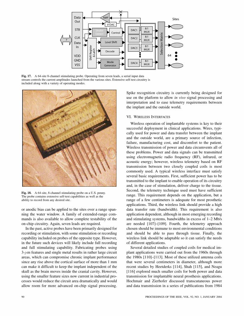
Fig. 17. A 64-site 8-channel stimulating probe. Operating from seven leads, a serial input datastream controls the current amplitudes launched from the various sites. Extensive self-test circuitry isincluded along with a variety of operating modes.
Fig. 18. A 64-site, 8-channel stimulating probe on a U.S. penny.The probe contains extensive self-test capabilities as well as theability to record from any desired site.
or anodic bias can be applied to the sites over a range span-ning the water window. A family of extended-range com-mands is also available to allow complete testability of theon-chip circuitry. Again, seven leads are required.
In the past, active probes have been primarily designed forrecording or stimulation, with some stimulation or recordingcapability included on probes of the opposite type. However,in the future such devices will likely include full recordingand full stimulating capability. Fabricating probes using3- m features and single metal results in rather large circuitareas, which can compromise chronic implant performancesince any rise above the cortical surface of more than 1 mmcan make it difficult to keep the implant independent of theskull as the brain moves inside the cranial cavity. However,using the smaller feature sizes now current in industrial pro-cesses would reduce the circuit area dramatically and wouldallow room for more advanced on-chip signal processing.
Spike recognition circuitry is currently being designed foruse on the platform to allow in vivo signal processing andinterpretation and to ease telemetry requirements betweenthe implant and the outside world.
VI. WIRELESS INTERFACES
Wireless operation of implantable systems is key to theirsuccessful deployment in clinical applications. Wires, typi-cally used for power and data transfer between the implantand the outside world, are a primary source of infection,failure, manufacturing cost, and discomfort to the patient.Wireless transmission of power and data circumvents all ofthese problems. Power and data signals can be transmittedusing electromagnetic radio frequency (RF), infrared, oracoustic energy; however, wireless telemetry based on RFtransmission between two closely coupled coils is mostcommonly used. A typical wireless interface must satisfyseveral basic requirements. First, sufficient power has to betransmitted to the implant to enable operation of its circuitryand, in the case of stimulation, deliver charge to the tissue.Second, the telemetry technique used must have sufficientrange. This requirement depends on the application, but arange of a few centimeters is adequate for most prostheticapplications. Third, the wireless link should provide a highdata transfer rate (bandwidth). This requirement is alsoapplication dependent, although in most emerging recordingand stimulating systems, bandwidths in excess of 1–2 Mb/sare needed [107]–[109]. Fourth, the telemetry approachchosen should be immune to most environmental conditionsand should be able to pass through tissue. Finally, thewireless link should be adaptable so it can satisfy the needsof different applications.
Several detailed studies of coupled coils for medical im-plant applications were carried out from the 1960s throughthe 1980s [110]–[113]. Most of these utilized antenna coilsthat were several centimeters in diameter, although morerecent studies by Heetderks [114], Shah [115], and Neagu[116] explored much smaller coils for both power and datatransmission for implantable neural prosthesis applications.Hochmair and Zierhofer discussed transcutaneous powerand data transmission in a series of publications from 1984
90 PROCEEDINGS OF THE IEEE, VOL. 92, NO. 1, JANUARY 2004
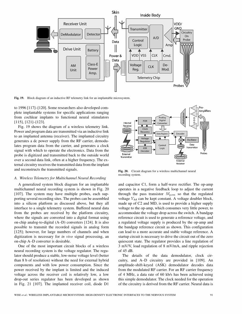
Fig. 19. Block diagram of an inductive RF telemetry link for an implantable microsystem.
to 1996 [117]–[120]. Some researchers also developed com-plete implantable systems for specific applications rangingfrom cochlear implants to functional neural stimulators[115], [121]–[123].
Fig. 19 shows the diagram of a wireless telemetry link.Power and program data are transmitted via an inductive linkto an implanted antenna (receiver). The implanted circuitrygenerates a dc power supply from the RF carrier, demodu-lates program data from the carrier, and generates a clocksignal with which to operate the electronics. Data from theprobe is digitized and transmitted back to the outside worldover a second data link, often at a higher frequency. The ex-ternal circuitry receives the transmitted data from the implantand reconstructs the transmitted signals.
A. Wireless Telemetry for Multichannel Neural Recording
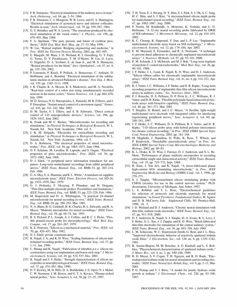
A generalized system block diagram for an implantablemultichannel neural recording system is shown in Fig. 20[107]. The system may have multiple probes, each sup-porting several recording sites. The probes can be assembledinto a silicon platform as discussed above, but they allinterface to a single telemetry system. Buffered neural datafrom the probes are received by the platform circuitry,where the signals are converted into a digital format usingon-chip analog-to-digital (A–D) converters [124]. It is alsopossible to transmit the recorded signals in analog form[125]; however, for large numbers of channels and whendigitization is necessary for in vivo signal processing, anon-chip A–D converter is desirable.
One of the most important circuit blocks of a wirelessneural recording system is the voltage regulator. The regu-lator should produce a stable, low-noise voltage level (betterthan 8 b of resolution) without the need for external hybridcomponents and with low power consumption. Since thepower received by the implant is limited and the inducedvoltage across the receiver coil is relatively low, a lowdrop-out series regulator has been developed as shownin Fig. 21 [107]. The implanted receiver coil, diode D1
Fig. 20. Circuit diagram for a wireless multichannel neuralrecording system.
and capacitor C1, form a half-wave rectifier. The op-ampoperates in a negative feedback loop to adjust the currentthrough the pass transistor so that the regulatedvoltage can be kept constant. A voltage doubler block,made up of C2 and MD, is used to provide a higher supplyvoltage to the op-amp, which consumes very little power, toaccommodate the voltage drop across the switch. A bandgapreference circuit is used to generate a reference voltage, anda regulated voltage supply is produced by the op-amp andthe bandgap reference circuit as shown. This configurationcan lead to a more accurate and stable voltage reference. Astartup circuit is necessary to drive the circuit out of the zeroquiescent state. The regulator provides a line regulation of3 mV/V, load regulation of 8 mV/mA, and ripple rejectionof 45 dB.
The details of the data demodulator, clock cir-cuitry, and A–D circuitry are provided in [109]. Anamplitude-shift-keyed (ASK) demodulator decodes datafrom the modulated RF carrier. For an RF carrier frequencyof 4 MHz, a data rate of 60 kb/s has been achieved usingthis simple demodulator. The clock needed for the operationof the circuitry is derived from the RF carrier. Neural data is
WISE et al.: WIRELESS IMPLANTABLE MICROSYSTEMS: HIGH-DENSITY ELECTRONIC INTERFACES TO THE NERVOUS SYSTEM 91
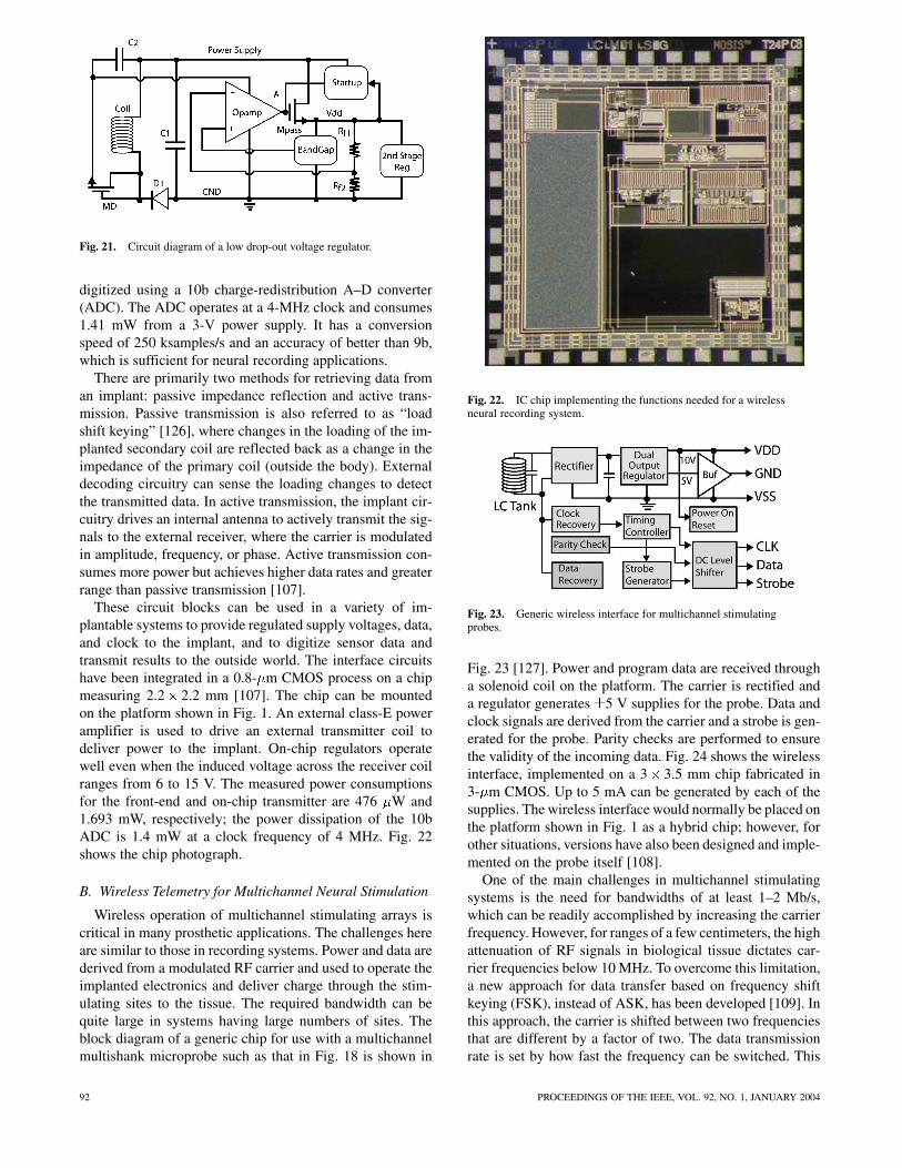
Fig. 21. Circuit diagram of a low drop-out voltage regulator.
digitized using a 10b charge-redistribution A–D converter(ADC). The ADC operates at a 4-MHz clock and consumes1.41 mW from a 3-V power supply. It has a conversionspeed of 250 ksamples/s and an accuracy of better than 9b,which is sufficient for neural recording applications.
There are primarily two methods for retrieving data froman implant: passive impedance reflection and active trans-mission. Passive transmission is also referred to as “loadshift keying” [126], where changes in the loading of the im-planted secondary coil are reflected back as a change in theimpedance of the primary coil (outside the body). Externaldecoding circuitry can sense the loading changes to detectthe transmitted data. In active transmission, the implant cir-cuitry drives an internal antenna to actively transmit the sig-nals to the external receiver, where the carrier is modulatedin amplitude, frequency, or phase. Active transmission con-sumes more power but achieves higher data rates and greaterrange than passive transmission [107].
These circuit blocks can be used in a variety of im-plantable systems to provide regulated supply voltages, data,and clock to the implant, and to digitize sensor data andtransmit results to the outside world. The interface circuitshave been integrated in a 0.8- m CMOS process on a chipmeasuring 2.2 2.2 mm [107]. The chip can be mountedon the platform shown in Fig. 1. An external class-E poweramplifier is used to drive an external transmitter coil todeliver power to the implant. On-chip regulators operatewell even when the induced voltage across the receiver coilranges from 6 to 15 V. The measured power consumptionsfor the front-end and on-chip transmitter are 476 W and1.693 mW, respectively; the power dissipation of the 10bADC is 1.4 mW at a clock frequency of 4 MHz. Fig. 22shows the chip photograph.
B. Wireless Telemetry for Multichannel Neural Stimulation
Wireless operation of multichannel stimulating arrays iscritical in many prosthetic applications. The challenges hereare similar to those in recording systems. Power and data arederived from a modulated RF carrier and used to operate theimplanted electronics and deliver charge through the stim-ulating sites to the tissue. The required bandwidth can bequite large in systems having large numbers of sites. Theblock diagram of a generic chip for use with a multichannelmultishank microprobe such as that in Fig. 18 is shown in
Fig. 22. IC chip implementing the functions needed for a wirelessneural recording system.
Fig. 23. Generic wireless interface for multichannel stimulatingprobes.
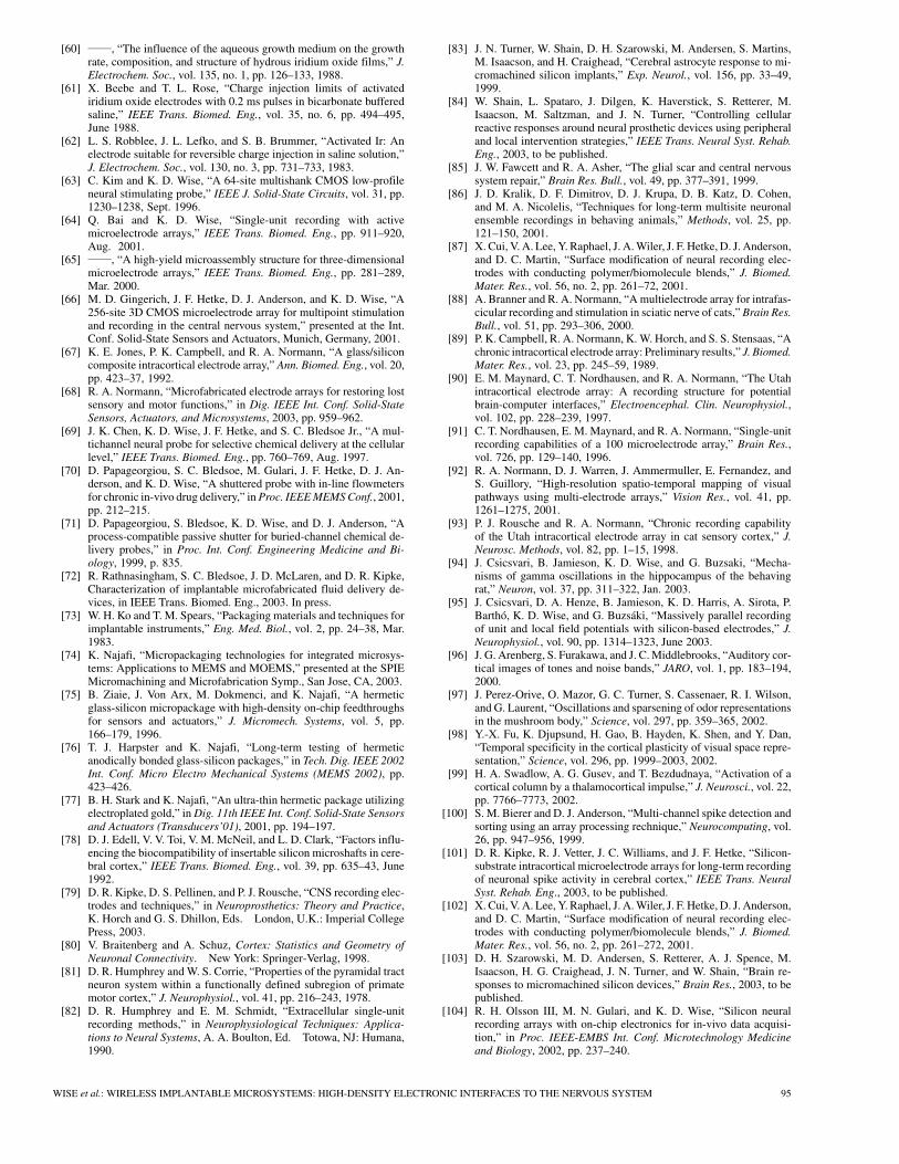
Fig. 23 [127]. Power and program data are received througha solenoid coil on the platform. The carrier is rectified anda regulator generates 5 V supplies for the probe. Data andclock signals are derived from the carrier and a strobe is gen-erated for the probe. Parity checks are performed to ensurethe validity of the incoming data. Fig. 24 shows the wirelessinterface, implemented on a 3 3.5 mm chip fabricated in3- m CMOS. Up to 5 mA can be generated by each of thesupplies. The wireless interface would normally be placed onthe platform shown in Fig. 1 as a hybrid chip; however, forother situations, versions have also been designed and imple-mented on the probe itself [108].
One of the main challenges in multichannel stimulatingsystems is the need for bandwidths of at least 1–2 Mb/s,which can be readily accomplished by increasing the carrierfrequency. However, for ranges of a few centimeters, the highattenuation of RF signals in biological tissue dictates car-rier frequencies below 10 MHz. To overcome this limitation,a new approach for data transfer based on frequency shiftkeying (FSK), instead of ASK, has been developed [109]. Inthis approach, the carrier is shifted between two frequenciesthat are different by a factor of two. The data transmissionrate is set by how fast the frequency can be switched. This
92 PROCEEDINGS OF THE IEEE, VOL. 92, NO. 1, JANUARY 2004
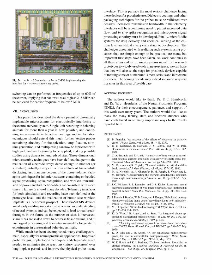
Fig. 24. A 3- � 3.5-mm chip in 3-�m CMOS implementing theinterface for a wireless stimulating probe.
switching can be performed at frequencies of up to 60% ofthe carrier, implying that bandwidths as high as 2–3 MHz canbe achieved for carrier frequencies below 5 MHz.
VII. CONCLUSION
This paper has described the development of chronicallyimplantable microsystems for electronically interfacing tothe central nervous system. Single-unit recording in behavinganimals for more than a year is now possible, and contin-uing improvements in bioactive coatings and implantationtechniques should extend this much further. Active probescontaining circuitry for site selection, amplification, stim-ulus generation, and multiplexing can now be fabricated withhigh yield and are beginning to be applied, making possiblestudies using dozens to hundreds of sites. Three-dimensionalmicroassembly techniques have been defined that permit therealization of electrode arrays dense enough to monitor (orstimulate) virtually every cell within a block of tissue whiledisplacing less than one percent of the tissue volume. Pack-aging techniques for full microsystems containing embeddedsignal processing, spike recognition, and wireless transmis-sion of power and bidirectional data are consistent with meantimes to failure in vivo of many decades. Telemetry interfacesfor both stimulation and recording have been defined at theprototype level, and the realization of button-size wirelessimplants is a near-term prospect. These bioMEMS devicesare already yielding important advances in our understandingof neural systems and can be expected to lead to real break-throughs in the future as the number of sites is increased,shank sizes are scaled down to decrease tissue trauma, and invivo signal processing and telemetry are used for longer-termexperiments in unrestrained behaving animals.
While much has been accomplished, many challenges re-main, especially for neural prosthesis applications. Improvedprobe designs, implantation techniques, and chip coatings areneeded to minimize tissue reactions (injury responses) overlong implant periods and improve the physical probe–tissue
interface. This is perhaps the most serious challenge facingthese devices for prosthetic use. Dielectric coatings and otherpackaging techniques for the probes must be validated overdecades. Increased transmission bandwidth in the telemetryinterfaces will be a continuing need to permit increased dataflow, and in vivo spike recognition and micropower signalprocessing circuitry must be developed. Finally, microfluidicsystems for drug delivery and chemical sensing at the cel-lular level are still at a very early stage of development. Thechallenges associated with realizing such systems using pro-cesses that are simple enough to be practical are many, butimportant first steps have been taken. As work continues inall these areas and as full microsystems move from researchprototypes to widely used tools in neuroscience, we can hopethat they will also set the stage for prosthetic devices capableof treating some of humankind’s most serious and intractabledisorders. The coming decade may indeed see some very realmiracles in this area of health care.
ACKNOWLEDGMENT
The authors would like to thank Dr. F. T. Hambrechtand Dr. W. J. Heetderks of the Neural Prosthesis Program,NINDS, for their encouragement, patience, and support ofthis work over many years. The authors would also like tothank the many faculty, staff, and doctoral students whohave contributed in so many important ways to the resultsreported here.
REFERENCES
[1] B. Franklin, “An account of the effects of electricity in paralyticcases,” Philos. Trans., vol. 50, pp. 481–483, 1759.
[2] R. C. Gesteland, B. Howland, J. Y. Lettvin, and W. H. Pitts,“Comments on microelectrodes,” Proc. IRE, vol. 47, pp. 1856–1862,1959.
[3] C. A. Terzuolo and T. Araki, “An analysis of intra-versus extra-cel-lular potential changes associated with activity of single spinal mo-toneurons,” Ann. NY Acad. Sci., vol. 94, pp. 547–558, 1963.
[4] M. Verseano and K. Negishi, “Neuronal activity in cortical and tha-lamic networks,” J. Gen. Physiol., vol. 43, pp. 177–195, 1960.
[5] M. A. Nicolelis, A. A. Ghazanfar, B. M. Faggin, S. Votaw, and L.M. Oliveira, “Reconstructing the engram: Simultaneous, multisite,many single neuron recordings,” Neuron, vol. 18, pp. 529–537, Apr.1997.
[6] J. C. Williams, R. L. Rennaker, and D. R. Kipke, “Long-term neuralrecording characteristics of wire microelectrode arrays implanted incerebral cortex,” Brain Res. Protocols, vol. 4, pp. 303–313, Dec.1999.
[7] I. Porada, I. Bondar, W. B. Spatz, and J. Kruger, “Rabbit and monkeyvisual cortex: More than a year of recording with up to 64 microelec-trodes,” J. Neurosci. Methods, vol. 95, pp. 13–28, 1999.
[8] M. P. Lepselter, “Beam-lead technology,” Bell Syst. Tech. J., vol. 45,pp. 233–254, Feb. 1966.
[9] K. D. Wise, J. B. Angell, and A. Starr, “An integrated circuit ap-proach to extracellular microelectrodes,” in Dig. 8th Int. Conf. En-gineering Medicine and Biology, 1969, p. 14.5.
[10] , “An integrated circuit approach to extracellular microelec-trodes,” IEEE Trans. Biomed. Eng., vol. BME-17, pp. 238–247, July1970.
[11] K. D. Wise and J. B. Angell, “A low-capacitance multielectrodeprobe for use in extracellular neurophysiology,” IEEE Trans.Biomed. Eng., vol. BME-22, pp. 212–219, May 1975.
[12] W. F. House and K. I. Berliner, “Cochlear implants: From idea toclinical practice,” in Cochlear Implants: A Practical Guide, H.Cooper, Ed. San Diego, CA: Singular, 1991, pp. 9–33.
WISE et al.: WIRELESS IMPLANTABLE MICROSYSTEMS: HIGH-DENSITY ELECTRONIC INTERFACES TO THE NERVOUS SYSTEM 93
[13] F. B. Simmons, “Electrical stimulation of the auditory nerve in man,”Arch. Otolaryng., vol. 84, pp. 2–54, 1966.
[14] F. B. Simmons, C. J. Mongeon, W. R. Lewis, and D. A. Huntington,“Electrical stimulation of acoustical nerve and inferior colliculus:Results in man,” Arch. Otolaryngol., vol. 79, pp. 559–567, 1964.
[15] G. S. Brindley and W. S. Lewin, “The sensations produced by elec-trical stimulation of the visual cortex,” J. Physiol., vol. 196, pp.479–493, May 1968.
[16] F. A. Spelman, “The past, present, and future of cochlear pros-theses,” IEEE Eng. Med. Biol. Mag., pp. 27–33, May 1999.
[17] W. Lui, “Retinal implant: Bridging engineering and medicine,” inProc. IEEE Int. Electron Devices Meeting, 2002, pp. 492–495.
[18] E. Margalit, M. Maia, J. D. Weiland, R. J. Greenberg, G. Y. Fujii,G. Torres, D. V. Piyathaisere, T. M. O’Hearn, W. Liu, G. Lazzi,G. Dagnelie, D. A. Scribner, E. de Juan Jr., and M. S. Humayun,“Retinal prosthesis for the blind,” Surv. Ophthalmol., vol. 47, no. 4,pp. 335–356, 2002.
[19] P. Limousin, P. Krack, P. Pollack, A. Benazzouz, C. Ardouin, D.Hoffmann, and A. Benabid, “Electrical stimulation of the subtha-lamic nucleus in advanced Parkinson’s disease,” New Eng. J. Med.,vol. 339, pp. 1105–1111, 1998.
[20] J. K. Chapin, K. A. Moxon, R. S. Markowitz, and M. A. Nicolelis,“Real-time control of a robot arm using simultaneously recordedneurons in the motor cortex,” Nature Neurosci., vol. 2, pp. 664–670,July 1999.
[21] M. D. Serruya, N. G. Hatsopoulos, L. Paninski, M. R. Fellows, and J.P. Donoghue, “Instant neural control of a movement signal,” Nature,vol. 416, pp. 141–142, Mar. 2002.
[22] D. M. Taylor, S. I. Tillery, and A. B. Schwartz, “Direct corticalcontrol of 3-D neuroprosthetic devices,” Science, vol. 296, pp.1829–1832, June 2002.
[23] K. Frank and M. C. Becker, “Microelectrodes for recording andstimulation,” in Physical Techniques in Biological Research, W. L.Nastuk, Ed. New York: Academic, 1964, vol. 5.
[24] J. R. M. Delgado, “Electrodes for extracellular recording andstimulation,” in Physical Techniques in Biological Research, W. L.Nastuk, Ed. New York: Academic, 1964, vol. 5.
[25] D. A. Robinson, “The electrical properties of metal microelec-trodes,” Proc. IEEE, vol. 56, pp. 1065–1071, June 1968.
[26] O. F. Schanne, M. Lavallee, R. Laprade, and S. Gagne, “Electricalproperties of glass microelectrodes,” Proc. IEEE, vol. 56, pp.1072–1082, June 1968.
[27] D. J. Edell, “A peripheral nerve information transducer for am-putees: Long-term multichannel recordings from rabbit peripheralnerves,” IEEE Trans. Biomed. Eng., vol. BME-33, pp. 203–214,Feb. 1986.
[28] G. A. May, S. A. Shamma, and R. L. White, “A tantalum-on-sapphiremicroelectrode array,” IEEE Trans. Electron Devices, vol. ED-26,pp. 1932–1939, Dec. 1979.
[29] O. J. Prohaska, F. Olcaytug, P. Pfundner, and H. Dragaun,“Thin-film multiple electrode probes: Possibilities and limitations,”IEEE Trans. Biomed. Eng., vol. BME-33, pp. 223–229, Feb. 1986.
[30] M. Kuperstein and D. A. Whittington, “A practical 24-channelmicroelectrode for neural recording in-vivo,” IEEE Trans. Biomed.Eng., vol. BME-28, pp. 288–293, Mar. 1981.
[31] N. A. Blum, B. G. Carkhuff, H. K. Charles, R. L. Edwards, and R. A.Meyer, “Multisite microprobes for neural recordings,” IEEE Trans.Biomed. Eng., vol. 38, pp. 68–74, Jan. 1991.
[32] R. S. Pickard, P. L. Joseph, A. J. Collins, and R. C. J. Hicks, “Flex-ible printed-circuit probe for electrophysiology,” Med. Biol. Eng.Comput., vol. 17, pp. 261–267, 1979.
[33] K. E. Petersen, “Silicon as a mechanical material,” Proc. IEEE, vol.70, pp. 420–457, May 1982.
[34] D. J. Edell, private communication.[35] K. Najafi, J. Ji, and K. D. Wise, “Scaling limitations of silicon mul-
tichannel recording probes,” IEEE Trans. Biomed. Eng., vol. 37, pp.1–11, Jan. 1990.
[36] C. Huang and K. Najafi, “Fabrication of ultrathin p++ silicon mi-crostructures using ion implantation and boron etch-stop,” J. Micro-electromech. Systems, vol. 10, pp. 532–537, Dec. 2001.
[37] K. Najafi and J. F. Hetke, “Strength characterization of silicon mi-croprobes in neurophysiological tissues,” IEEE Trans. Biomed. Eng.,vol. 37, pp. 474–481, May 1990.
[38] D. T. Kewley, M. D. Hills, D. A. Borkholder, I. E. Opris, N. I. Maluf,C. W. Storment, J. M. Bower, and G. T. A. Kovacs, “Plasma-etchedneural probes,” Sens. Actuators A, vol. 58, pp. 27–35, 1997.
[39] T. H. Yoon, E. J. Hwang, D. Y. Shin, S. I. Park, S. J. Oh, S. C. Jung,H. C. Shin, and S. J. Kim, “A micromachined silicon depth probefor multichannel neural recording,” IEEE Trans. Biomed. Eng., vol.47, pp. 1082–1087, Aug. 2000.
[40] P. Norlin, M. Kindlundh, A. Mouroux, K. Yoshida, and U. G.Hofmann, “A 32-site neural recording probe fabricated by DRIEof SOI substrates,” J. Micromech. Microeng., vol. 12, pp. 414–419,2002.
[41] K. C. Cheung, K. Djupsund, Y. Dan, and L. P. Lee, “Implantablemultichannel electrode array based on SOI technology,” J. Micro-electromech. Systems, vol. 12, pp. 179–184, Apr. 2003.
[42] E. M. Maynard, E. Fernandez, and R. A. Normann, “A techniqueto prevent dural adhesions to chronically implanted microelectrodearrays,” J. Neurosci. Methods, vol. 97, pp. 93–101, 2000.
[43] E. M. Schmidt, J. S. McIntosh, and M. J. Bak, “Long-term implantsof parylene-C coated microelectrodes,” Med. Biol. Eng., vol. 26, pp.96–101, 1988.
[44] J. F. Hetke, J. L. Lund, K. Najafi, K. D. Wise, and D. J. Anderson,“Silicon ribbon cables for chronically implantable microelectrodearrays,” IEEE Trans. Biomed. Eng., vol. 41, no. 4, pp. 314–321, Apr.1994.
[45] R. J. Vetter, J. C. Williams, J. F. Hetke, and D. R. Kipke, “Long-termrecording properties of implantable thin-film silicon microelectrodearrays in auditory cortex,” Soc. Neurosci. Abstr., 2002.
[46] P. J. Rousche, D. S. Pellinen, D. P. Pivin Jr., J. C. Williams, R. J.Vetter, and D. R. Kirke, “Flexible polyimide-based intracortical elec-trode arrays with bioactive capability,” IEEE Trans. Biomed. Eng.,vol. 48, pp. 361–371, Mar. 2001.
[47] T. Stieglitz, H. Beutel, and J.-U. Meyer, “A flexible, light-weightmultichannel sieve electrode with integrated cables for interfacingregenerating peripheral nerves,” Sens. Actuators A, vol. 60, pp.240–243, 1997.
[48] J. F. Hetke, J. C. Williams, D. S. Pellinen, R. J. Vetter, and D. R.Kipke, “3-D silicon probe array with hybrid polymer interconnectfor chronic cortical recording,” in Proc. IEEE EMBS Special TopicConf. Neural Engineering, 2003, pp. 181–184.
[49] M. Maghribi, J. Hamilton, D. Polla, K. Rose, T. Wilson, andP. Krulevitch, “Stretchable microelectrode array,” in Proc. Int.IEEE-EMBS Special Topics Conf. Microtechnologies Medicine andBiology, 2002, pp. 80–83.
[50] K. L. Drake, K. D. Wise, J. Farraye, D. J. Anderson, and S. L. Be-Ment, “Performance of planar multisite microprobes in recordingextracellular single-unit intracortical activity,” IEEE Trans. Biomed.Eng., vol. 35, pp. 719–732, Sept. 1988.
[51] B. Ziaie, J. Von Arx, and K. Najafi, “A micro-fabricated planarhigh-current IrOx stimulating microelectrode,” in Proc. IEEEEngineering Medicine and Biology (EMBS) Conf., vol. 1, 1996, pp.270–271.
[52] S. J. Tanghe, “Micromachined silicon stimulating probes withCMOS circuitry for use in the central nervous system,” Ph.D.dissertation, University of Michigan, Ann Arbor, 1992.
[53] L. S. Robblee and T. L. Rose, “Electrochemical guidelinesfor selection of protocols and electrode materials for neuralstimulation,” in Neural Prosthesis: Fundamental Studies, W. Agnewand D. B. McCreery, Eds. Englewood Cliffs, NJ: Prentice-Hall,1990, ch. 2.
[54] J. D. Weiland and D. J. Anderson, “Chronic neural stimulation withthin-film, iridium oxide electrodes,” IEEE Trans. Biomed. Eng., vol.47, pp. 911–918, 2000.
[55] D. J. Anderson, K. Najafi, S. J. Tanghe, D. A. Evans, K. L. Levy, J.F. Hetke, X. L. Xue, J. J. Zappia, and K. D. Wise, “Batch-fabricatedthin-film electrodes for stimulation of the central auditory system,”IEEE Trans. Biomed. Eng., vol. 36, pp. 693–704, July 1989.
[56] L. M. Schiavone, W. C. Dautremont-Smith, G. Beni, and J. L. Shay,“Improved electrochromic behavior of reactively sputtered iridiumoxide films,” J. Electrochem. Soc., vol. 128, no. 6, pp. 1339–1342,1981.
[57] B. Aurian-Blajeni, M. M. Boucher, A. G. Kimball, and L. S. Rob-blee, “Physiochemical characterization of sputtered iridium oxide,”J. Mater. Res., vol. 4, no. 2, pp. 440–446, 1989.
[58] R. D. Meyer, S. F. Cogan, T. H. Nguyen, and R. D. Rauh, “Elec-trodeposited iridium oxide for neural stimulation and recording elec-trodes,” IEEE Trans. Neural Syst. Rehab. Eng., vol. 9, pp. 2–11, Mar.2001.
[59] P. G. Pickup and V. I. Birss, “A model for anodic hydrous oxidegrowth at iridium,” J. Electroanal. Chem., vol. 220, pp. 83–100,1987.
94 PROCEEDINGS OF THE IEEE, VOL. 92, NO. 1, JANUARY 2004
[60] , “The influence of the aqueous growth medium on the growthrate, composition, and structure of hydrous iridium oxide films,” J.Electrochem. Soc., vol. 135, no. 1, pp. 126–133, 1988.
[61] X. Beebe and T. L. Rose, “Charge injection limits of activatediridium oxide electrodes with 0.2 ms pulses in bicarbonate bufferedsaline,” IEEE Trans. Biomed. Eng., vol. 35, no. 6, pp. 494–495,June 1988.
[62] L. S. Robblee, J. L. Lefko, and S. B. Brummer, “Activated Ir: Anelectrode suitable for reversible charge injection in saline solution,”J. Electrochem. Soc., vol. 130, no. 3, pp. 731–733, 1983.
[63] C. Kim and K. D. Wise, “A 64-site multishank CMOS low-profileneural stimulating probe,” IEEE J. Solid-State Circuits, vol. 31, pp.1230–1238, Sept. 1996.
[64] Q. Bai and K. D. Wise, “Single-unit recording with activemicroelectrode arrays,” IEEE Trans. Biomed. Eng., pp. 911–920,Aug. 2001.
[65] , “A high-yield microassembly structure for three-dimensionalmicroelectrode arrays,” IEEE Trans. Biomed. Eng., pp. 281–289,Mar. 2000.
[66] M. D. Gingerich, J. F. Hetke, D. J. Anderson, and K. D. Wise, “A256-site 3D CMOS microelectrode array for multipoint stimulationand recording in the central nervous system,” presented at the Int.Conf. Solid-State Sensors and Actuators, Munich, Germany, 2001.
[67] K. E. Jones, P. K. Campbell, and R. A. Normann, “A glass/siliconcomposite intracortical electrode array,” Ann. Biomed. Eng., vol. 20,pp. 423–37, 1992.
[68] R. A. Normann, “Microfabricated electrode arrays for restoring lostsensory and motor functions,” in Dig. IEEE Int. Conf. Solid-StateSensors, Actuators, and Microsystems, 2003, pp. 959–962.
[69] J. K. Chen, K. D. Wise, J. F. Hetke, and S. C. Bledsoe Jr., “A mul-tichannel neural probe for selective chemical delivery at the cellularlevel,” IEEE Trans. Biomed. Eng., pp. 760–769, Aug. 1997.
[70] D. Papageorgiou, S. C. Bledsoe, M. Gulari, J. F. Hetke, D. J. An-derson, and K. D. Wise, “A shuttered probe with in-line flowmetersfor chronic in-vivo drug delivery,” in Proc. IEEE MEMS Conf., 2001,pp. 212–215.
[71] D. Papageorgiou, S. Bledsoe, K. D. Wise, and D. J. Anderson, “Aprocess-compatible passive shutter for buried-channel chemical de-livery probes,” in Proc. Int. Conf. Engineering Medicine and Bi-ology, 1999, p. 835.
[72] R. Rathnasingham, S. C. Bledsoe, J. D. McLaren, and D. R. Kipke,Characterization of implantable microfabricated fluid delivery de-vices, in IEEE Trans. Biomed. Eng., 2003. In press.
[73] W. H. Ko and T. M. Spears, “Packaging materials and techniques forimplantable instruments,” Eng. Med. Biol., vol. 2, pp. 24–38, Mar.1983.
[74] K. Najafi, “Micropackaging technologies for integrated microsys-tems: Applications to MEMS and MOEMS,” presented at the SPIEMicromachining and Microfabrication Symp., San Jose, CA, 2003.
[75] B. Ziaie, J. Von Arx, M. Dokmenci, and K. Najafi, “A hermeticglass-silicon micropackage with high-density on-chip feedthroughsfor sensors and actuators,” J. Micromech. Systems, vol. 5, pp.166–179, 1996.
[76] T. J. Harpster and K. Najafi, “Long-term testing of hermeticanodically bonded glass-silicon packages,” in Tech. Dig. IEEE 2002Int. Conf. Micro Electro Mechanical Systems (MEMS 2002), pp.423–426.
[77] B. H. Stark and K. Najafi, “An ultra-thin hermetic package utilizingelectroplated gold,” in Dig. 11th IEEE Int. Conf. Solid-State Sensorsand Actuators (Transducers’01), 2001, pp. 194–197.
[78] D. J. Edell, V. V. Toi, V. M. McNeil, and L. D. Clark, “Factors influ-encing the biocompatibility of insertable silicon microshafts in cere-bral cortex,” IEEE Trans. Biomed. Eng., vol. 39, pp. 635–43, June1992.
[79] D. R. Kipke, D. S. Pellinen, and P. J. Rousche, “CNS recording elec-trodes and techniques,” in Neuroprosthetics: Theory and Practice,K. Horch and G. S. Dhillon, Eds. London, U.K.: Imperial CollegePress, 2003.
[80] V. Braitenberg and A. Schuz, Cortex: Statistics and Geometry ofNeuronal Connectivity. New York: Springer-Verlag, 1998.
[81] D. R. Humphrey and W. S. Corrie, “Properties of the pyramidal tractneuron system within a functionally defined subregion of primatemotor cortex,” J. Neurophysiol., vol. 41, pp. 216–243, 1978.
[82] D. R. Humphrey and E. M. Schmidt, “Extracellular single-unitrecording methods,” in Neurophysiological Techniques: Applica-tions to Neural Systems, A. A. Boulton, Ed. Totowa, NJ: Humana,1990.
[83] J. N. Turner, W. Shain, D. H. Szarowski, M. Andersen, S. Martins,M. Isaacson, and H. Craighead, “Cerebral astrocyte response to mi-cromachined silicon implants,” Exp. Neurol., vol. 156, pp. 33–49,1999.
[84] W. Shain, L. Spataro, J. Dilgen, K. Haverstick, S. Retterer, M.Isaacson, M. Saltzman, and J. N. Turner, “Controlling cellularreactive responses around neural prosthetic devices using peripheraland local intervention strategies,” IEEE Trans. Neural Syst. Rehab.Eng., 2003, to be published.
[85] J. W. Fawcett and R. A. Asher, “The glial scar and central nervoussystem repair,” Brain Res. Bull., vol. 49, pp. 377–391, 1999.
[86] J. D. Kralik, D. F. Dimitrov, D. J. Krupa, D. B. Katz, D. Cohen,and M. A. Nicolelis, “Techniques for long-term multisite neuronalensemble recordings in behaving animals,” Methods, vol. 25, pp.121–150, 2001.
[87] X. Cui, V. A. Lee, Y. Raphael, J. A. Wiler, J. F. Hetke, D. J. Anderson,and D. C. Martin, “Surface modification of neural recording elec-trodes with conducting polymer/biomolecule blends,” J. Biomed.Mater. Res., vol. 56, no. 2, pp. 261–72, 2001.
[88] A. Branner and R. A. Normann, “A multielectrode array for intrafas-cicular recording and stimulation in sciatic nerve of cats,” Brain Res.Bull., vol. 51, pp. 293–306, 2000.
[89] P. K. Campbell, R. A. Normann, K. W. Horch, and S. S. Stensaas, “Achronic intracortical electrode array: Preliminary results,” J. Biomed.Mater. Res., vol. 23, pp. 245–59, 1989.
[90] E. M. Maynard, C. T. Nordhausen, and R. A. Normann, “The Utahintracortical electrode array: A recording structure for potentialbrain-computer interfaces,” Electroencephal. Clin. Neurophysiol.,vol. 102, pp. 228–239, 1997.
[91] C. T. Nordhausen, E. M. Maynard, and R. A. Normann, “Single-unitrecording capabilities of a 100 microelectrode array,” Brain Res.,vol. 726, pp. 129–140, 1996.
[92] R. A. Normann, D. J. Warren, J. Ammermuller, E. Fernandez, andS. Guillory, “High-resolution spatio-temporal mapping of visualpathways using multi-electrode arrays,” Vision Res., vol. 41, pp.1261–1275, 2001.
[93] P. J. Rousche and R. A. Normann, “Chronic recording capabilityof the Utah intracortical electrode array in cat sensory cortex,” J.Neurosc. Methods, vol. 82, pp. 1–15, 1998.
[94] J. Csicsvari, B. Jamieson, K. D. Wise, and G. Buzsaki, “Mecha-nisms of gamma oscillations in the hippocampus of the behavingrat,” Neuron, vol. 37, pp. 311–322, Jan. 2003.
[95] J. Csicsvari, D. A. Henze, B. Jamieson, K. D. Harris, A. Sirota, P.Barthó, K. D. Wise, and G. Buzsáki, “Massively parallel recordingof unit and local field potentials with silicon-based electrodes,” J.Neurophysiol., vol. 90, pp. 1314–1323, June 2003.
[96] J. G. Arenberg, S. Furakawa, and J. C. Middlebrooks, “Auditory cor-tical images of tones and noise bands,” JARO, vol. 1, pp. 183–194,2000.
[97] J. Perez-Orive, O. Mazor, G. C. Turner, S. Cassenaer, R. I. Wilson,and G. Laurent, “Oscillations and sparsening of odor representationsin the mushroom body,” Science, vol. 297, pp. 359–365, 2002.
[98] Y.-X. Fu, K. Djupsund, H. Gao, B. Hayden, K. Shen, and Y. Dan,“Temporal specificity in the cortical plasticity of visual space repre-sentation,” Science, vol. 296, pp. 1999–2003, 2002.
[99] H. A. Swadlow, A. G. Gusev, and T. Bezdudnaya, “Activation of acortical column by a thalamocortical impulse,” J. Neurosci., vol. 22,pp. 7766–7773, 2002.
[100] S. M. Bierer and D. J. Anderson, “Multi-channel spike detection andsorting using an array processing rechnique,” Neurocomputing, vol.26, pp. 947–956, 1999.
[101] D. R. Kipke, R. J. Vetter, J. C. Williams, and J. F. Hetke, “Silicon-substrate intracortical microelectrode arrays for long-term recordingof neuronal spike activity in cerebral cortex,” IEEE Trans. NeuralSyst. Rehab. Eng., 2003, to be published.
[102] X. Cui, V. A. Lee, Y. Raphael, J. A. Wiler, J. F. Hetke, D. J. Anderson,and D. C. Martin, “Surface modification of neural recording elec-trodes with conducting polymer/biomolecule blends,” J. Biomed.Mater. Res., vol. 56, no. 2, pp. 261–272, 2001.
[103] D. H. Szarowski, M. D. Andersen, S. Retterer, A. J. Spence, M.Isaacson, H. G. Craighead, J. N. Turner, and W. Shain, “Brain re-sponses to micromachined silicon devices,” Brain Res., 2003, to bepublished.
[104] R. H. Olsson III, M. N. Gulari, and K. D. Wise, “Silicon neuralrecording arrays with on-chip electronics for in-vivo data acquisi-tion,” in Proc. IEEE-EMBS Int. Conf. Microtechnology Medicineand Biology, 2002, pp. 237–240.
WISE et al.: WIRELESS IMPLANTABLE MICROSYSTEMS: HIGH-DENSITY ELECTRONIC INTERFACES TO THE NERVOUS SYSTEM 95
[105] , “A fully-integrated bandpass amplifier for extracellular neuralrecording,” in Proc. 1st IEEE/EMBS Int. Conf. Neural Engineering,2003, pp. 165–168.
[106] Y. Yao, M. N. Gulari, J. F. Hetke, and K. D. Wise, “A self-testingmultiplexed CMOS stimulating probe for a 1024-site neural pros-thesis,” in Proc. IEEE Int. Conf. Solid-State Sensors, Actuators, andMicrosystems (Transducers’03), pp. 1213–1216.
[107] H. Yu and K. Najafi, “Low-power interface circuits for bio-im-plantable microsystems,” presented at the Int. IEEE Solid-StateCircuits Conf. (ISSCC) 2003, San Francisco, CA.
[108] M. Ghovanloo, K. D. Wise, and K. Najafi, “Toward a button-sized1024-site wireless cortical microstimulating array,” in Proc. 1st Int.IEEE/EMBS Conf. Neural Engineering, 2003, pp. 138–141.
[109] M. Ghovanloo and K. Najafi, “A fully-digital frequency-shift-keyingdemodulator chip for wireless biomedical implants,” in Proc. IEEESouthwest Symp. Mixed-Signal Design (SSMSD 2003), pp. 223–227.
[110] F. C. Flack, E. D. James, and D. M. Schlapp, “Mutual inductanceof air-cored coils: Effect on design or radio frequency coupled im-plants,” Med. Biol. Eng., vol. 9, pp. 79–85, 1971.
[111] W. H. Ko, S. P. Liang, and C. D. Fung, “Design of radio-frequencypowered coils for implant instruments,” Med. Biol. Eng. Comp., vol.15, pp. 634–640, 1977.
[112] M. Soma, D. G. Galbraith, and R. L. White, “Radio-frequency coilsin implantable devices: Misalignment analysis and design proce-dure,” IEEE Trans. Biomed. Eng., vol. BME-34, pp. 276–282, Apr.1987.
[113] D. G. Galbraith, M. Soma, and R. L. White, “A wide-band efficientinductive transdermal power and data link with coupling insensitivegain,” IEEE Trans. Biomed. Eng., vol. BME-34, pp. 265–275, Apr.1987.
[114] W. J. Heetderks, “RF powering of millimeter and submillimeter-sized neural prosthetic implants,” IEEE Trans. Biomed. Eng., vol.35, pp. 323–327, May 1988.
[115] M. R. Shah, R. P. Phillips, and R. A. Normann, “A study of printedspiral coils for neuroprosthetic transcranial telemetry applications,”IEEE Trans. Biomed. Eng., vol. 45, pp. 867–876, July 1998.
[116] C. R. Neagu, H. V. Jansen, A. Smith, J. G. E. Gardeniers, and M. C.Elwanspoek, “Characterization of a planar microcoil for implantablemicrosystems,” Sens. Actuators A, vol. 62, pp. 599–611, 1997.
[117] E. S. Hochmair, “System optimization for improved accuracy in tran-scutaneous signal and power transmission,” IEEE Trans. Biomed.Eng., vol. BME-31, no. 2, pp. 177–186, Feb. 1984.
[118] C. M. Zierhofer and E. S. Hochmair, “High-efficiency coupling-in-sensitive transcutaneous power and data transmission via an induc-tive link,” IEEE Trans. Biomed. Eng., vol. 37, no. 7, pp. 716–722,July 1990.
[119] , “Geometric approach for coupling enhancement of magneti-cally coupled coils,” IEEE Trans. Biomed. Eng., vol. 43, no. 7, pp.708–714, July 1996.
[120] , “The class-E concept for efficient wide-band coupling-in-sensitive transdermal power and data transfer,” in Proc. IEEE 14thEMBS Conf., vol. 2, 1992, pp. 382–383.
[121] H. McDermott, “An advanced multiple channel cochlear implant,”IEEE Trans. Biomed. Eng., vol. 36, no. 7, pp. 789–797, July 1989.
[122] , “A custom-designed receiver-stimulator chip for an advancedmultiple-channel hearing prosthesis,” IEEE J. Solid-State Circuits,vol. 26, pp. 1161–1164, Aug. 1991.
[123] B. Smith, P. H. Peckham, M. W. Keith, and D. D. Roscoe, “An ex-ternally powered, multichannel, implantable stimulator for versa-tile control of paralyzed muscle,” IEEE Trans. Biomed. Eng., vol.BME-34, no. 7, pp. 499–508, July 1987.
[124] T. Akin, K. Najafi, and R. M. Bradley, “A wireless implantablemultichannel digital neural recording system for a micromachinedsieve electrode,” IEEE J. Solid-State Circuits, pp. 109–118, Jan.1998.
[125] P. Mohseni and K. Najafi, “A wireless FM microsystem for biomed-ical neural recording applications,” in Proc. IEEE Southwest Symp.Mixed-Signal Design, 2003, pp. 217–222.
[126] Z. Tang, B. Smith, J. H. Schild, and P. H. Peckham, “Data trans-mission from an implantable biotelemeter by load-shift keying usingcircuit configuration modulator,” IEEE Trans. Biomed. Eng., vol. 42,pp. 524–528, May 1995.
[127] M. Ghovanloo, K. Beach, K. D. Wise, and K. Najafi, “A BiCMOSwireless interface chip for micromachined stimulating micro-probes,” Proc. IEEE-EMBS Special Topic Conf. MicrotechnologiesMedicine and Biology, pp. 277–282, 2002.
Kensall D. Wise received the B.S.E.E. degreewith highest distinction from Purdue University,West Lafayette, IN, in 1963 and the M.S. andPh.D. degrees in electrical engineering fromStanford University, Stanford, CA, in 1964 and1969, respectively.
From 1963 to 1965 (on leave 1965–1969) andfrom 1972 to 1974, he was a Member of TechnicalStaff at Bell Telephone Laboratories, where hiswork was concerned with the exploratory devel-opment of integrated electronics for use in tele-
phone communications. From 1965 to 1972, he was a Research Assistantand then a Research Associate and Lecturer in the Department of ElectricalEngineering at Stanford University, working on the development of inte-grated circuit technology and its application to solid-state sensors. In 1974,he joined the Department of Electrical Engineering and Computer Scienceat the University of Michigan, Ann Arbor, where he is now the J. Reid andPolly Anderson Professor of Manufacturing Technology and Director of theNSF Engineering Research Center for Wireless Integrated MicroSystems.His present research interests focus on the development of integrated mi-crosystems for health care, process control, and environmental monitoring.
Dr. Wise organized and served as the first chairman of the Technical Sub-committee on Solid-State Sensors of the IEEE Electron Devices Society(EDS). He was General Chairman of the 1984 IEEE Solid-State Sensor Con-ference, Technical Program Chairman of the IEEE International Conferenceon Solid-State Sensors and Actuators (1985), and IEEE-EDS National Lec-turer (1986). He served as General Chairman of the 1997 IEEE Interna-tional Conference on Solid-State Sensors and Actuators. Dr. Wise receivedthe Paul Rappaport Award from the EDS (1990), a Distinguished FacultyAchievement Award from the University of Michigan (1995), the ColumbusPrize from the Christopher Columbus Fellowship Foundation (1996), theSRC Aristotle Award (1997), and the 1999 IEEE Solid-State Circuits FieldAward. In 2002 he was named the William Gould Dow Distinguished Uni-versity Professor at the University of Michigan. He is a Fellow of the AIMBEand a Member of the U.S. National Academy of Engineering.
David J. Anderson received the B.S.E.E. degreefrom Rensselaer Polytechnic Institute, Troy, NY,in 1961 and the M.S. and Ph.D. degrees from theUniversity of Wisconsin, Madison, in 1963 and1968, respectively.
After completing a postdoctoral traineeshipwith the Laboratory of Neurophysiology, Uni-versity of Wisconsin Medical School, he joinedthe University of Michigan, Ann Arbor, wherehe is now professor of Electrical Engineeringand Computer Science, Biomedical Engineering,
Biomedical Engineering and Otolaryngology.Dr. Anderson is a Fellow of the American Institute for Medical and
Biological Engineering, a member of the IEEE Neuroscience Society,the Acoustical Society of America, the Association for Research inOtolaryngology, and the Barany Society.
Jamille F. Hetke received the B.S.E.E. degreefrom Michigan State University, East Lansing, in1985 and the M.S. degree in bioengineering fromthe University of Michigan, Ann Arbor, in 1987.
She has been involved in neural probe researchat the University of Michigan since the comple-tion of her degrees and is currently an AssistantResearch Scientist in the Department of ElectricalEngineering and Computer Science. She partici-pates in research in the Kresge Hearing ResearchInstitute and the Neural Engineering Laboratory,
and is the main contact for investigators interested in obtaining probes fromthe Center for Neural Communication Technology. Her research interestsare centered on the design of silicon arrays and implantable systems foreventual use in neuroprostheses.
96 PROCEEDINGS OF THE IEEE, VOL. 92, NO. 1, JANUARY 2004
Daryl R. Kipke (Member, IEEE) received theB.Sc. degree in engineering science, the M.Sc.degree in bioengineering, the M.S.E. degree inelectrical engineering, and the Ph.D. degree inbioengineering from the University of Michigan,Ann Arbor, in 1985, 1986, 1988, and 1991,respectively.
From 1991 to 1992, he was a Research Asso-ciate in the Department of Bioengineering and theInstitute for Sensory Research at Syracuse Uni-versity, Syracuse, NY. In 1992, he was appointed
Assistant Professor in Bioengineering at Arizona State University, Tempe,where his research was focused in auditory neurophysiology, computationalneuroscience, neuroprostheses, and bioMEMS. In 1998, he was promoted toAssociate Professor in Bioengineering. In 2001, he joined the faculty of theCollege of Engineering at the University of Michigan to continue his workin bioMEMS for neural implants, neuroprostheses and brain-machine inter-faces, systems neuroscience, and functional neurosurgery. He is currentlyan Associate Professor in the Departments of Biomedical Engineering andElectrical Engineering and Computer Science, University of Michigan, andthe Director of the Neural Engineering Laboratory.
Khalil Najafi (Fellow, IEEE) was born in 1958.He received the B.S., M.S., and Ph.D. degreesin electrical engineering from the Department ofElectrical Engineering and Computer Science,University of Michigan, Ann Arbor, in 1980,1981, and 1986 respectively.
Since 1986, he has been with the Departmentof Electrical Engineering and Computer Science,University of Michigan. From 1986 to 1988 hewas a Research Fellow; from 1988 to 1990, hewas an Assistant Research Scientist; from 1990
to 1993, he was an Assistant Professor; from 1993 to 1998 he was an As-sociate Professor; since September 1998, he has been a Professor and theDirector of the Solid-State Electronics Laboratory. He is an Associate Ed-itor for the Journal of Micromechanics and Microengineering and an Editorfor the Journal of Sensors and Materials. His research interests include mi-cromachining technologies, solid-state micromachined sensors, actuators,and MEMS; analog integrated circuits; implantable biomedical microsys-tems; hermetic micropackaging; and low-power wireless sensing/actuatingsystems.
Dr. Najafi was awarded a National Science Foundation Young Investi-gator Award from 1992 to 1997. He was the recipient of the Beatrice WinnerAward for Editorial Excellence at the 1986 International Solid-State CircuitsConference, the Paul Rappaport Award for coauthoring the Best Paper pub-lished in the IEEE Transactions on Electron Devices, and the Best PaperAward at ISSCC 1999. In 2001 he received the Faculty Recognition Award,and in 1994 the University of Michigan’s Henry Russel Award for out-standing achievement and scholarship, and was selected as the Professorof the Year in 1993. In 1998, he was named the Arhtur F. Thurnau Pro-fessor for outstanding contributions to teaching and research, and receivedthe College of Engineering’s Research Excellence Award. He has been ac-tive in the field of solid-state sensors and actuators for more than 18 years,and has been involved in several conferences and workshops dealing withsolid-state sensors and actuators, including the International Conference onSolid-State Sensors and Actuators, the Hilton-Head Solid-State Sensors andActuators Workshop, and the IEEE/ASME Micro Electromechanical Sys-tems (MEMS) Conference. He is the Editor for solid-state sensors for IEEETRANSACTIONS ON ELECTRON DEVICES and an Associate Editor for IEEEJOURNAL OF SOLID-STATE CIRCUITS.
WISE et al.: WIRELESS IMPLANTABLE MICROSYSTEMS: HIGH-DENSITY ELECTRONIC INTERFACES TO THE NERVOUS SYSTEM 97