Embed Size (px)
Citation preview
WLD
3343 GEN
ERA
L PUR
POSE D
RIVER
FOR
LASER
DIO
DES
www.teamWavelength.com© 2001-2015 WLD3343-00400-P
GENERAL DESCRIPTION:The WLD3343 is an easy-to-use analog circuit for space constrained laser diode applications. The WLD3343 maintains precision laser diode current (constant current mode) or stable photodiode current (constant power mode) regulation using electronics that are compatible with any laser diode type. Safely supply up to 3 Amps of current to your laser diode from a single +5 Volt power supply.
Excellent for VCSELs, electro-optical equipment, and medical/dental systems.
General Purpose Driver for Laser Diodes & VCSELs
FEATURES:• Low Cost• Slow Start Laser Diode Protection• Drive Up to 3 Amps Output Current• Constant Current or Power Operation• Compatible With Any Laser Diode Type• Small Package Size (1.30” X 1.26” X 0.313”)• Voltage Controlled Setpoint• TTL Compatible Shutdown Pin• Adjustable Current Limit• Adjustable Current Range• 2 MHz Constant Current Bandwidth• Over Temperature Shutdown• 14-Pin DIP PCB Mount
Figure 1Top View Pin Layout and Descriptions
WLD3343
1
2
3
4
5
6
7
14
13
12
11
10
9
8
TOP VIEW
SHDVSETIMONPMONMODELIMGND
VDDPD-PD+
OUTARS-
OUTBRS+
Shutdown Laser Diode Output Current
Setpoint Voltage Input
Laser Diode Current Monitor
Photodiode Current Monitor
Mode Configuration
Laser Diode Current Limit
Power Supply Ground
Power Supply Input
Photodiode Current Sense Resistor Negative Input
Photodiode Current Sense Resistor Positive Input
Output A
Laser Diode Current Sense Resistor Negative Input
Output B
Laser Diode Current Sense Resistor Positive Input
(BOTTOM VIEW)
Up to 500 mA
Add Heatsink & Thermal Washer for 1 A
Add Fan for 2 A
Pb
RoHS Com
plia
nte
Ordering InformationWLD3343WLD3343HBWLD3343-3AWLD3343-2LWLD3343-3LWLD3393
WTW002WHS302WXC303WXC304
2.2 A Laser Diode Driver2.2 A Li+ Battery-compatible Driver3 A Laser Diode Driver2.2 A Lower Noise Driver, no CP mode3 A Lower Noise Driver, no CP modeEvaluation PCB for WLD3343, WLD3343-3A, WLD3343-2L, and WLD3343-3LThermal Washer for all WLDsHeatsink for all WLDs+5 VDC Fan for all WLDs+12 VDC Fan for all WLDs
April, 2015
www.teamWavelength.com© 2001-2015
WLD
3343PAGE 2
WLD3343-00400-P
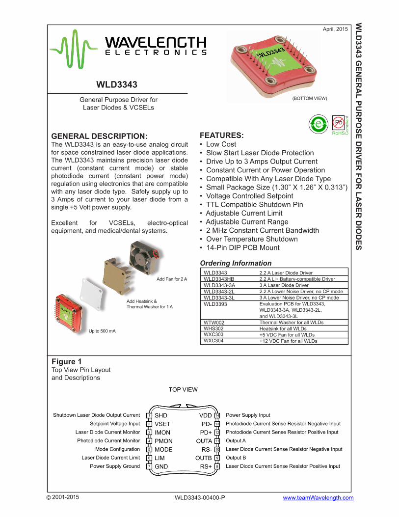
Figure 2Quick Connect Diagram For Type A/B Laser Diodes Operated in Constant Current Mode
1
2
3
4
5
6
7
14
13
12
11
10
9
8
WLD3343LASERDIODE
DRIVER
VDD
RLIM
1 TIE GROUND CONNECTIONS DIRECTLY TO PIN 7
RSENSE
ENABLE
DISABLE
IMON
NC
1 k
1
1
1
LD PD LD PD
OR
VDD
D/AOR ORBandgap
VoltageReference
See Eq. 7
Constant Current: See Eq. 5
VSET
AdjustingLimit CurrentSee Table 2and Eq. 3
Adjusting LaserDiode Current RangeSee Table 1 or Eq. 1
1
1
RPD IPD =VPD+
-
VPD
RPD
2k
Part # LM4040www.national.com
1k
LDMAXSENSE I
00.1R
With Eval Board (Rev. Level)
Without Evaluation Board
=
VSET = (Desired ILD) * (2*RSENSE)
LD Range RSENSE (Rev. C)
2.0 A200 mA
438 m5.01
RSENSE (Rev. A&B)
500 m5.1
TOP VIEW
An online tool is available to determine values for external components:
http://www.teamwavelength.com/support/tools.asp.
www.teamWavelength.com© 2001-2015
WLD
3343PAGE 3
WLD3343-00400-P
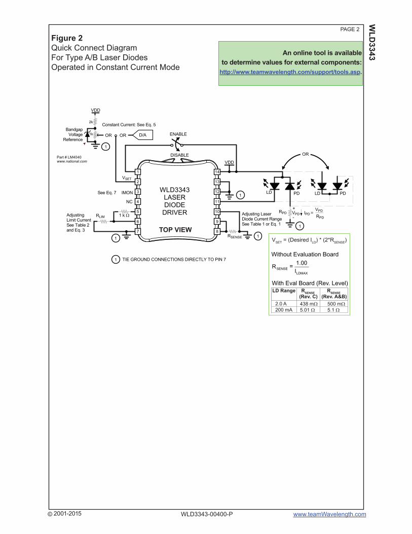
Supply Voltage (Voltage on Pin 14)Output Current (See SOA Chart)Power Dissipation, TAMBIENT = +25˚COperating Temperature, case [2]Storage TemperatureWeight
ELECTRICAL AND OPERATING SPECIFICATIONS
Volts DCAmperesWatts [1]˚C˚Coz
UNITVALUE+4.5 to +12.52.2 or 39- 40 to + 85 [3]- 65 to +1500.6
VDD
ILD
PMAX
TOPR
TSTG
WLD3343
ABSOLUTE MAXIMUM RATINGSRATING SYMBOL
AmpsVoltsVoltsVoltsVoltsVoltsVoltsVoltsVoltsnsecnsecMHz
SecondsSeconds
mA
ppm
%%
3
2.8
9.8
200
2.2
200
10.610.410.1
4603202.0
(Depends on PD BW)
0.240.01
0
OUTPUTCurrent, peak, see SOA chartCompliance Voltage, Laser Diode LoadCompliance Voltage, Laser Diode LoadCompliance Voltage, Laser Diode LoadCompliance Voltage, Laser Diode LoadCompliance Voltage, Laser Diode LoadCompliance Voltage, Laser Diode LoadCompliance Voltage, Laser Diode LoadCompliance Voltage, Laser Diode LoadRise TimeFall TimeBandwidthBandwidthSlow Start - DelaySlow Start - RampLeakage Current [4]CONSTANT CURRENT CONTROLShort Term Stability, 1 hourCONSTANT POWER CONTROLShort Term Stability, 1 hourLong Term Stability, 24 hours
WLD3343-2A UNITSTEST CONDITIONSPARAMETER
ILD = 100 mA, 5 VILD = 1.0 Amp, 5 VILD = 2.0 Amps, 5 VILD = 3.0 Amps, 5 VILD = 100 mA,12 VILD = 1.0 Amp,12 VILD = 2.0 Amp,12 VILD = 3.0 Amp,12 VILD= Full ScaleILD= Full ScaleConstant Current, Sine Wave, 2 AConstant Power
TAMBIENT = 25˚C
TAMBIENT = 25˚CTAMBIENT = 25˚C
Notes:[1] In the WLD3343 and WLD3343-2L models, internal power dissipation is 1.2 W (without heatsink), 2 W (with heatsink), and 9 W (with heatsink and fan). In the WLD3343-3A and WLD3343-3L models, internal power dissipation is 2 W (without heatsink), 3 W (with heatsink), and 10 W (with heatsink and fan).[2] With Revision D forward of the WLD3343, an internal thermostat has been added to activate Shutdown (SHD) when the internal temperature exceeds 105˚C. The output will be re-enabled after a 250 to 300 msec slow-start once the internal temperature drops below 95˚C.[3] Max ambient operating temperature of the WLD3343-3A and WLD3343-3L is 45°C.[4] Leakage current specifi cation is based on full current set by RSENSE. See page 9 for information on setting the current range. Minimum turn on current in the 200 mA range is 350 μA. Minimum turn on current in the 2 A range is 12 mA. This specifi cation applies to Rev. E forward.
Noise: To further reduce noise, the WLD3343-2L and WLD3343-3L models are available. Both are about 2.5 times lower noise than the WLD3343 and WLD3343-3A, respectively. Constant Power (CP) mode is not available in these models.
0.010.05
WLD3343-3A
3.63.53.0

www.teamWavelength.com© 2001-2015
WLD
3343PAGE 4
WLD3343-00400-P
mVμAV
dBV
˚C / W˚C / W˚C / W
Seconds
VoltsmA
%
%%
1-50 to 150
0 to 280
> VDD + 0.5 or < -0.5
3021.53.4
10
5 to 1210
0.5
3.33.5
INPUTOffset Voltage, initial, Imon
VSET Bias Current (1)
VSET Input Voltage RangePower Supply RejectionVSET (Pin 2) Damage ThresholdTHERMALHeatspreader Temperature RiseHeatspreader Temperature RiseHeatspreader Temperature Rise
Pin SolderabilityPOWER SUPPLYVoltage, VDD
Current, VDD supply, quiescentMONITOR ACCURACYMonitor Voltage versus Expected Output Current, based on transfer functionPD Monitor versus ActualSetpoint versus Actual
Pin 2, TAMBIENT = 25˚C, VCM = 0 V
Full Temperature Range
TAMBIENT = 25˚CWith WHS302 Heat sink, WTW002 Thermal Washer With WHS302 Heat sink, WTW002 Thermal Washer and 3.5 CFM fanSolder temp @260˚C
ELECTRICAL AND OPERATING SPECIFICATIONS - Continued
UNITSTEST CONDITIONSPARAMETER WLD3343-2A WLD3343-3A
Notes:[1] As VSET approaches zero volts, the VSET signal source must sink up to 50 μA. As VSET approaches 2 V, the VSET signal source must source up to 150 μA.

www.teamWavelength.com© 2001-2015
WLD
3343PAGE 5
WLD3343-00400-P
Float or connect a zero Volt signal to Pin 1 (SHD) to ENABLE the output current to the laser diode.Connect a +3 Volt or greater signal to Pin 1 (SHD) to DISABLE the output current to the laser diode.Connect a voltage source between Pin 2 (VSET) and Pin 7 (GND) to control either the laser diode current in constant current mode or laser diode power in constant power mode. Range is 0-2.0 volt full scale. Input impedance is 20 kΩ. The offset voltage is 0.5V when open (applies to Revision D forward). Do not let the input pin fl oat or damage to the load may result.Monitor the laser diode forward current using Pin 3 (IMON). TheLaser Diode Current Monitor produces a voltage proportional tothe current fl owing through the laser diode.Monitor the laser diode power using Pin 4 (PMON). ThePhotodiode Current Monitor produces a voltage proportional to the current produced by the laser diode monitor photodiode.CONSTANT CURRENT OPERATION:A 1k resistor between Pin 5 (MODE) and Pin 6 (LIM) confi gures the WLD3343 to regulate the laser diode’s forward current.CONSTANT POWER OPERATION:A 0.1 μF capacitor between Pin 5 (MODE) and Pin 6 (LIM) confi gures the WLD3343 to regulate the laser diode’s output power.A resistor connected between Pin 6 (LIM) and Pin 7 (GND) limitsthe maximum amount of forward current through the laser diodeConnect the VDD power supply ground connection to Pin 7 (GND).Connect Pin 8 (RS+) directly to the positive side of the laser diode current sense resistor. The resistance value of RSENSE determines the range of forward current through the laser diode.Connect Pin 9 (OUTB) to the positive side of RSENSE.Connect Pin 10 (RS-) directly to the negative side of the laser diode current sense resistor. The resistance value of RSENSE determines the range of forward current through the laser diode.
PIN DESCRIPTIONS
Shutdown Laser Diode Output Current
Setpoint Voltage Input or Modulation Input
Laser Diode Current Monitor
Photodiode Current Monitor
Mode Confi guration
Laser Diode Current Limit
Power Supply Ground
Laser Diode Current SenseResistor Positive Input
Output BLaser Diode Current SenseResistor Negative Input
SHD
VSET
IMON
PMON
MODE
LIM
GND
RS+
OUTBRS-
1
2
3
4
5
6
7
8
910
Pin Pin # Name Function
Pin Descriptions continued on the next page.
www.teamWavelength.com© 2001-2015
WLD
3343PAGE 6
WLD3343-00400-P
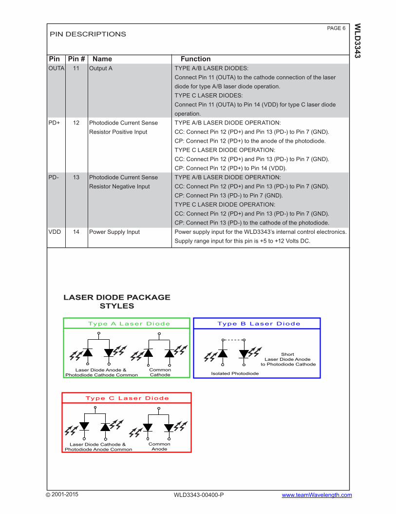
TYPE A/B LASER DIODES:Connect Pin 11 (OUTA) to the cathode connection of the laser diode for type A/B laser diode operation.TYPE C LASER DIODES:Connect Pin 11 (OUTA) to Pin 14 (VDD) for type C laser diodeoperation.TYPE A/B LASER DIODE OPERATION:CC: Connect Pin 12 (PD+) and Pin 13 (PD-) to Pin 7 (GND).CP: Connect Pin 12 (PD+) to the anode of the photodiode.TYPE C LASER DIODE OPERATION:CC: Connect Pin 12 (PD+) and Pin 13 (PD-) to Pin 7 (GND).CP: Connect Pin 12 (PD+) to Pin 14 (VDD).TYPE A/B LASER DIODE OPERATION:CC: Connect Pin 12 (PD+) and Pin 13 (PD-) to Pin 7 (GND).CP: Connect Pin 13 (PD-) to Pin 7 (GND).TYPE C LASER DIODE OPERATION:CC: Connect Pin 12 (PD+) and Pin 13 (PD-) to Pin 7 (GND).CP: Connect Pin 13 (PD-) to the cathode of the photodiode.Power supply input for the WLD3343’s internal control electronics.Supply range input for this pin is +5 to +12 Volts DC.
LASER DIODE PACKAGE STYLES
Type A Laser Diode Type B Laser Diode
CommonCathode
Laser Diode Anode & Photodiode Cathode Common Isolated Photodiode
Short Laser Diode Anode
to Photodiode Cathode
OUTA
PD+
PD-
VDD
11
12
13
14
Output A
Photodiode Current SenseResistor Positive Input
Photodiode Current SenseResistor Negative Input
Power Supply Input
Type C Laser Diode
CommonAnode
Laser Diode Cathode & Photodiode Anode Common
PIN DESCRIPTIONS
Pin Pin # Name Function

www.teamWavelength.com© 2001-2015
WLD
3343PAGE 7
WLD3343-00400-P
Caution:Do not exceed the Safe Operating Area (SOA). Exceeding the SOA voids the warranty.
An online tool is available for calculating Safe Operating Area at: http://www.teamwavelength.com/support/calculator/soa/soald.php.
To determine if the operating parameters fall within the SOA of the device, the maximum voltage drop across the controller and the maximum current must be plotted on the SOA curves.These values are used for the example SOA determination:
Vs = 12 voltsVLoad = 5 voltsILoad = 1 amp
Follow these steps:1. Determine the maximum voltage drop across the driver,Vs-VLoad, and mark on the X axis. Example: 12 volts - 5 volts = 7 volts, Point A)2. Determine the maximum current, ILoad, through the driver and mark on the Y axis: (1 amp, Point B)3. Draw a horizontal line through Point B across the chart. (Line BB)4. Draw a vertical line from Point A to the maximum current line indicated by Line BB.5. Mark VS on the X axis. (Point C)6. Draw the Load Line from where the vertical line from point A intersects Line BB down to Point C.
Refer to the chart shown below and note that the Load Line is in the Unsafe Operating Areas for use with no heatsink (1) or the heatsink alone (2), but is outside of the Unsafe Operating Area for use with heatsink and Fan (3).
These values are determined from the specifi cations of the laser diode.}
Graphs assume:25°C Ambient75°C Case
A
B BB
C
SAFE OPERATING AREA & HEATSINK REQUIREMENTS

www.teamWavelength.com© 2001-2015
WLD
3343PAGE 8
WLD3343-00400-P
Caution:Do not exceed the Safe Operating Area (SOA). Exceeding the SOA voids the warranty.
An online tool is available for calculating Safe Operating Area at: http://www.teamwavelength.com/support/calculator/soa/soald.php.
To determine if the operating parameters fall within the SOA of the device, the maximum voltage drop across the controller and the maximum current must be plotted on the SOA curves.These values are used for the example SOA determination:
Vs = 9 voltsVLoad = 6 voltsILoad = 2.5 amps
Follow these steps:1. Determine the maximum voltage drop across the driver,Vs-VLoad, and mark on the X axis. Example: 9 volts - 6 volts = 3 volts, Point A)2. Determine the maximum current, ILoad, through the driver and mark on the Y axis: (2.5 amps, Point B)3. Draw a horizontal line through Point B across the chart. (Line BB)4. Draw a vertical line from Point A to the maximum current line indicated by Line BB.5. Mark VS on the X axis. (Point C)6. Draw the Load Line from where the vertical line from point A intersects Line BB down to Point C.
Refer to the chart shown below. Note that the Load Line is in the Safe Operating Area for use with heatsink and fan (3). It is in the Unsafe Operating Area for use with no heatsink (1) or the heatsink alone (2).
These values are determined from the specifi cations of the laser diode.}
Graphs assume:25°C Ambient75°C Case
A
B BB
C
SAFE OPERATING AREA & HEATSINK REQUIREMENTS
www.teamWavelength.com© 2001-2015
WLD
3343PAGE 9
WLD3343-00400-P
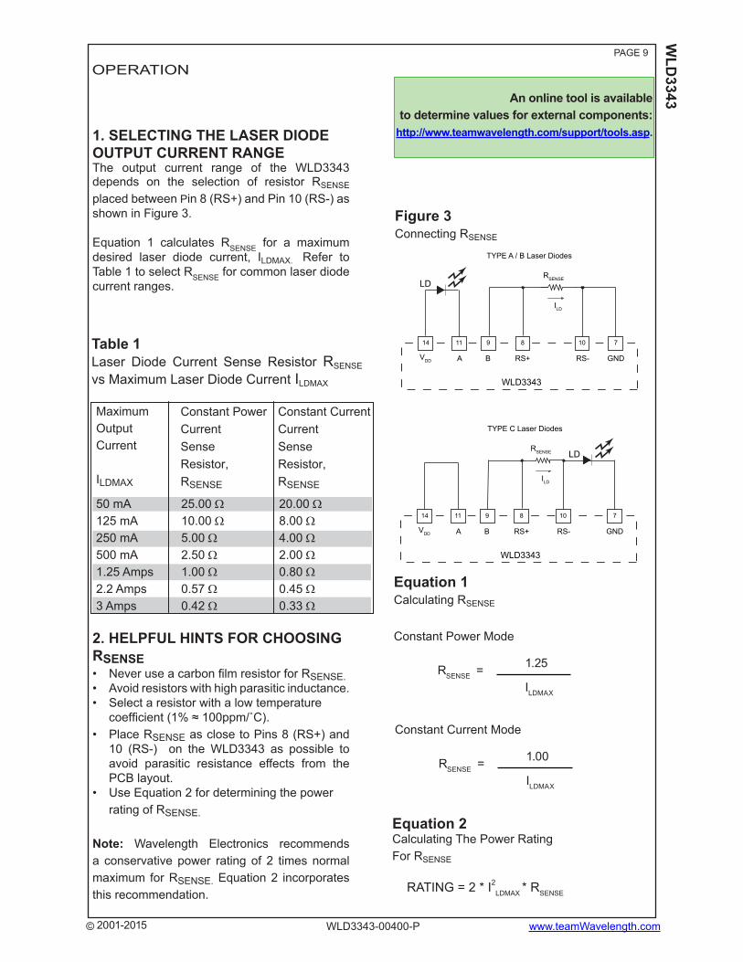
1. SELECTING THE LASER DIODE OUTPUT CURRENT RANGE The output current range of the WLD3343 depends on the selection of resistor RSENSE placed between Pin 8 (RS+) and Pin 10 (RS-) as shown in Figure 3.
Equation 1 calculates RSENSE for a maximum desired laser diode current, ILDMAX. Refer to Table 1 to select RSENSE for common laser diode current ranges.
2. HELPFUL HINTS FOR CHOOSING RSENSE• Never use a carbon fi lm resistor for RSENSE.• Avoid resistors with high parasitic inductance.• Select a resistor with a low temperature
coeffi cient (1% ≈ 100ppm/˚C).• Place RSENSE as close to Pins 8 (RS+) and
10 (RS-) on the WLD3343 as possible to avoid parasitic resistance effects from the PCB layout.
• Use Equation 2 for determining the power rating of RSENSE.
Note: Wavelength Electronics recommends a conservative power rating of 2 times normal maximum for RSENSE. Equation 2 incorporates this recommendation.
Table 1Laser Diode Current Sense Resistor RSENSE vs Maximum Laser Diode Current ILDMAX
Figure 3Connecting RSENSE
Equation 1Calculating RSENSE
Constant Power Mode
RSENSE = 1.25 ILDMAX
OPERATION
Equation 2Calculating The Power Rating For RSENSE
RATING = 2 * I2LDMAX * RSENSE
TYPE A / B Laser Diodes
A B GNDVDD
11 9 1014
WLD3343
LDRSENSE
8 7
RS+ RS-
ILD
TYPE C Laser Diodes
A B GNDVDD
11 9 1014
WLD3343
LDRSENSE
8 7
RS+ RS-
ILD
Constant Current Mode
RSENSE = 1.00 ILDMAX
Constant Current CurrentSenseResistor,RSENSE
MaximumOutputCurrent
ILDMAX
Constant Power CurrentSenseResistor,RSENSE
50 mA125 mA250 mA500 mA1.25 Amps2.2 Amps3 Amps
25.00 10.00 5.00 2.50 1.00 0.57 0.42
20.00 8.00 4.00 2.00 0.80 0.45 0.33
An online tool is available to determine values for external components:
http://www.teamwavelength.com/support/tools.asp.
www.teamWavelength.com© 2001-2015
WLD
3343PAGE 10
WLD3343-00400-P
Example 1Choosing RLIM for a Type A/B Laser Diode with a 1.5 A Maximum Forward Current in Constant Current Mode.Confi gure the WLD3343 so that ILDMAX is 2.2 A by selecting R
SENSE equal to 0.45 . The Normalized
Maximum Output Current then equals:
A Normalized Output Current of 0.68 (68%) corresponds to a current limit set resistor RLIM of 405 .
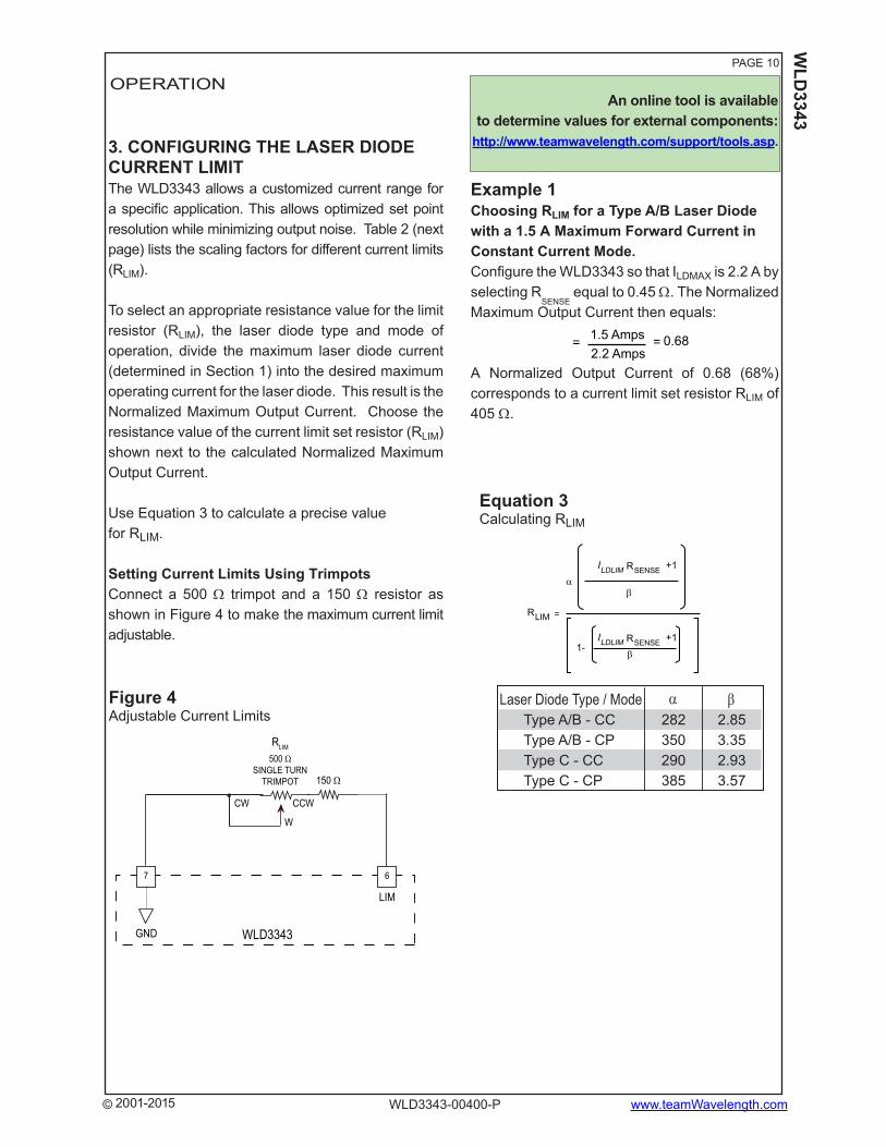
3. CONFIGURING THE LASER DIODE CURRENT LIMIT The WLD3343 allows a customized current range for a specifi c application. This allows optimized set point resolution while minimizing output noise. Table 2 (next page) lists the scaling factors for different current limits (RLIM).
To select an appropriate resistance value for the limit resistor (RLIM), the laser diode type and mode of operation, divide the maximum laser diode current (determined in Section 1) into the desired maximum operating current for the laser diode. This result is the Normalized Maximum Output Current. Choose the resistance value of the current limit set resistor (RLIM) shown next to the calculated Normalized Maximum Output Current.
Use Equation 3 to calculate a precise value for RLIM.
Setting Current Limits Using TrimpotsConnect a 500 trimpot and a 150 resistor as shown in Figure 4 to make the maximum current limit adjustable.
Figure 4Adjustable Current Limits
Equation 3Calculating RLIM
= =1.5 Amps2.2 Amps
0.68
α
ILDLIM RSENSE +1
ILDLIM RSENSE +1
β
RLIM =
β1-
GND
7
WLD3343
RLIM
6
LIM
CW CCW
W
150
500 SINGLE TURN
TRIMPOT
OPERATION
Laser Diode Type / Mode Type A/B - CCType A/B - CPType C - CCType C - CP
282350290385
2.853.352.933.57
An online tool is available to determine values for external components:
http://www.teamwavelength.com/support/tools.asp.

www.teamWavelength.com© 2001-2015
WLD
3343PAGE 11
WLD3343-00400-P
Table 2Current Limit Set Resistor RLIM vs Normalized Maximum Output Current
Normalized Maximum Output Current
Type A/B Laser Diode Constant Current Limit Set Resistor RLIM ( )
Type C Laser Diode Constant Current Limit Set Resistor RLIM ( )
Type C Laser Diode Constant Power Limit Set Resistor RLIM ( )
Type A/B Laser Diode Constant Power Limit Set Resistor RLIM ( )
0.00 (0%)0.04 (4%)0.08 (8%)0.12 (12%)0.16 (16%)0.20 (20%)0.24 (24%)0.28 (28%)0.32 (32%)0.36 (36%)0.40 (40%)0.44 (44%)0.48 (48%)0.52 (52%)0.56 (56%)0.60 (60%)0.64 (64%)0.68 (68%)0.72 (72%)0.76 (76%)0.80 (80%)0.84 (84%)0.88 (88%)0.92 (92%)0.96 (96%)1.00 (100%)
152162172183194205217230243257272288305322341361382405429455483514547582621664
149160171183195208222236251267284301320340361383406432459488519552588627670716
150160169179190201213225238251265280296313330349369390412436462490519551586624
150160171183195207220234248263279295313331350370392414438463490519550583618656
OPERATIONAn online tool is available
to determine values for external components:http://www.teamwavelength.com/support/tools.asp.
www.teamWavelength.com© 2001-2015
WLD
3343PAGE 12
WLD3343-00400-P
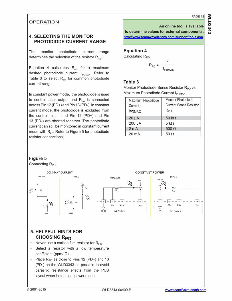
4. SELECTING THE MONITORPHOTODIODE CURRENT RANGE
The monitor photodiode current range determines the selection of the resistor RPD.
Equation 4 calculates RPD for a maximum desired photodiode current, IPDMAX. Refer to Table 3 to select RPD for common photodiode current ranges.
In constant power mode, the photodiode is used to control laser output and RPD is connected across Pin 12 (PD+) and Pin 13 (PD-). In constant current mode, the photodiode is excluded from the control circuit and Pin 12 (PD+) and Pin 13 (PD-) are shorted together. The photodiode current can still be monitored in constant current mode with RPD. Refer to Figure 5 for photodiode resistor connections.
Figure 5Connecting RPD
Equation 4Calculating RPD
Table 3Monitor Photodiode Sense Resistor RPD vs Maximum Photodiode Current IPDMAX
20 μA 50 k200 μA 5 k2 mA 500 20 mA 50
Maximum Photodiode Current, IPDMAX
Monitor Photodiode Current Sense Resistor, RPD
PDR =1
IPDMAX
TYPE A / B TYPE C
GND GND
RPD
RPD
VDD
OR
OR
CONSTANT CURRENT
TYPE A / B TYPE C
PD- PD+
GND GND
VDD VDDPD- PD+
7 713 1312 1214 14
OR
PIN 11
WLD3343 WLD3343
OR
PIN 10
RPD RPD
CONSTANT POWER
OPERATION
5. HELPFUL HINTS FOR CHOOSING RPD• Never use a carbon fi lm resistor for RPD.• Select a resistor with a low temperature
coeffi cient (ppm/˚C).• Place RPD as close to Pins 12 (PD+) and 13
(PD-) on the WLD3343 as possible to avoid parasitic resistance effects from the PCB layout when in constant power mode.
An online tool is available to determine values for external components:
http://www.teamwavelength.com/support/tools.asp.

www.teamWavelength.com© 2001-2015
WLD
3343PAGE 13
WLD3343-00400-P
Figure 6Disabling Output Current
14 1
VDD WLD3343
ENABLE
DISABLE
SHUTDOWN SWITCH
SHD
14 1
VDD WLD3343 SHD
TTL INPUT
ENABLE
DISABLE
OR
6. DISABLING OUTPUT CURRENTThe output current can be enabled and disabled as shown in Figure 6 using a SPST (Single-Pole Single-Throw) switch or a TTL signal.
NOTE:Do not insert or remove the laser diode from the WLD3343 circuit with power applied to the unit.
OPERATION

www.teamWavelength.com© 2001-2015
WLD
3343PAGE 14
WLD3343-00400-P
1
2
3
4
5
6
7
14
13
12
11
10
9
8
WLD3343LASERDIODE
DRIVER
VDD
RPD
RLIM
1 TIE GROUND CONNECTIONS DIRECTLY TO PIN 7
RSENSE
ENABLE
DISABLE
IMON
PMON
0.1 F
1
1
1
LD PD LD PD
OR
VDD
D/AOR ORBandgap
VoltageReference
See Eq. 7
See Eq. 9
Constant Power: See Eq. 6
VSET
AdjustingLimit CurrentSee Table 2and Eq. 3
Adjusting Laser DiodeCurrent RangeSee Table 1 or Eq. 1
Adjusting PhotodiodeCurrent RangeSee Table 3 or Eq. 4
1
2k
www.national.comPart #LM4040
1k
PDMAXPD I
1R
With Evaluation Board
Without Evaluation Board
=
VSET = (Desired IPD) * (2*RPD)
PD Range RPD
2.0 mA200 A
499 4.99 k
LDMAXSENSE I
25.1R
With Eval Board (Rev. Level)
Without Evaluation Board
=
LD Range RSENSE (Rev. C)
2.0 A200 mA
438 m5.01
RSENSE (Rev. A&B)
500 m5.1
1
2
3
4
5
6
7
14
13
12
11
10
9
8
WLD3343LASERDIODE
DRIVER
VDD
RLIM
1 TIE GROUND CONNECTIONS DIRECTLY TO PIN 7
RSENSE
ENABLE
DISABLE
IMON
NC
1 k
1
1
1
LD PD LD PD
OR
VDD
D/AOR ORBandgap
VoltageReference
See Eq. 7
Constant Current: See Eq. 5
VSET
AdjustingLimit CurrentSee Table 2and Eq. 3
Adjusting LaserDiode Current RangeSee Table 1 or Eq. 1
1
1
RPD IPD =VPD+
-
VPD
RPD
2k
Part # LM4040www.national.com
1k
LDMAXSENSE I
00.1R
With Eval Board (Rev. Level)
Without Evaluation Board
=
VSET = (Desired ILD) * (2*RSENSE)
LD Range RSENSE (Rev. C)
2.0 A200 mA
438 m5.01
RSENSE (Rev. A&B)
500 m5.1
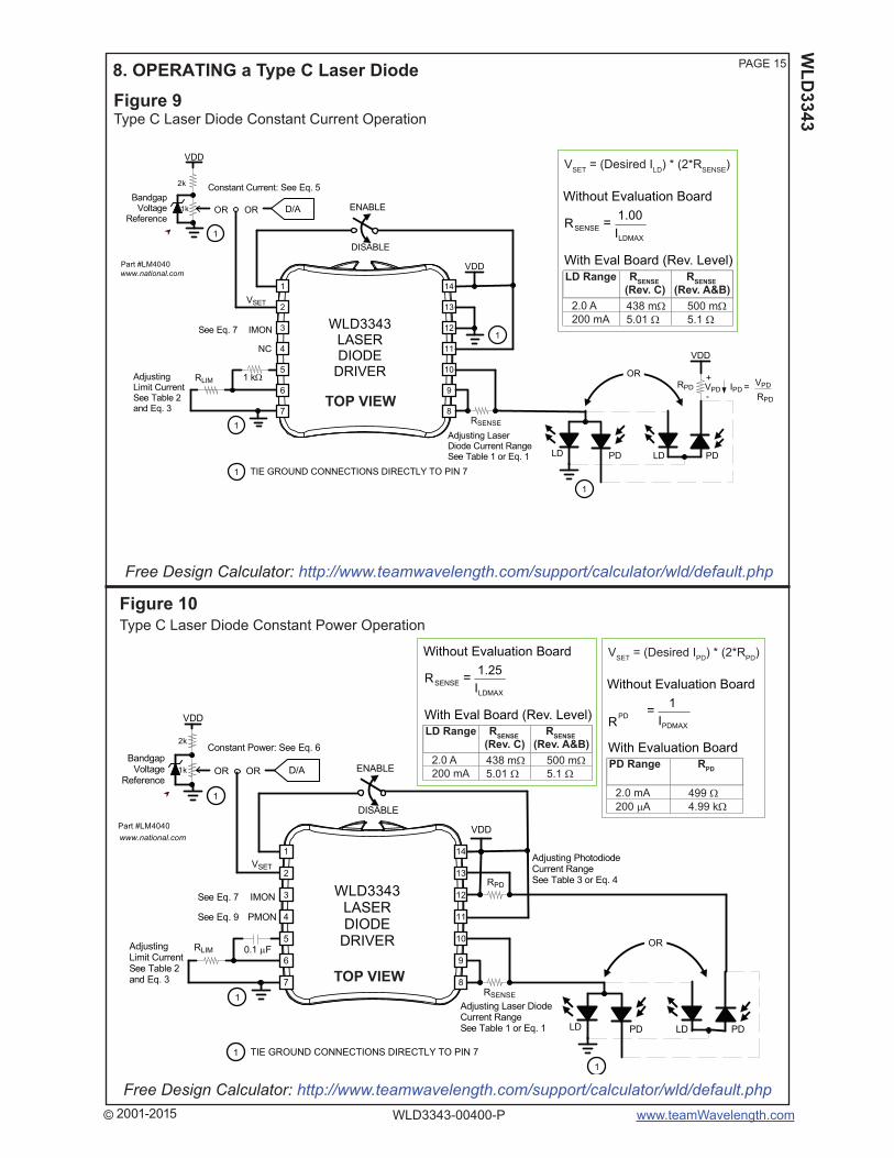
Free Design Calculator: http://www.teamwavelength.com/support/calculator/wld/default.php
7. OPERATING a Type A/B Laser DiodeFigure 7A/B Laser Diode Constant Current Operation
Figure 8A/B Laser Diode Constant Power Operation
Free Design Calculator: http://www.teamwavelength.com/support/calculator/wld/default.php
TOP VIEW
TOP VIEW
www.teamWavelength.com© 2001-2015
WLD
3343PAGE 15
WLD3343-00400-P
1
2
3
4
5
6
7
14
13
12
11
10
9
8
WLD3343LASERDIODE
DRIVER
RPD
RLIM
1 TIE GROUND CONNECTIONS DIRECTLY TO PIN 7
RSENSE
ENABLE
DISABLE
IMON
PMON
0.1 F
1
VDD
D/AOR ORBandgap
VoltageReference
See Eq. 7
See Eq. 9
Constant Power: See Eq. 6
VSET
AdjustingLimit CurrentSee Table 2and Eq. 3
Adjusting Laser DiodeCurrent RangeSee Table 1 or Eq. 1
Adjusting PhotodiodeCurrent RangeSee Table 3 or Eq. 4
1
VDD
1
LD PD LD PD
OR
2k
Part #LM4040www.national.com
1k
PDMAXPD I
1R
With Evaluation Board
Without Evaluation Board
=
VSET = (Desired IPD) * (2*RPD)
PD Range RPD
2.0 mA200 A
499 4.99 k
LDMAXSENSE I
25.1R
With Eval Board (Rev. Level)
Without Evaluation Board
=
LD Range RSENSE (Rev. C)
2.0 A200 mA
438 m5.01
RSENSE (Rev. A&B)
500 m5.1
1
2
3
4
5
6
7
14
13
12
11
10
9
8
WLD3343LASERDIODE
DRIVER
VDD
RLIM
1 TIE GROUND CONNECTIONS DIRECTLY TO PIN 7
RSENSE
ENABLE
DISABLE
IMON
NC
1 k
1
1
1
LD PD LD PD
OR
VDD
D/AOR ORBandgap
VoltageReference
See Eq. 7
Constant Current: See Eq. 5
VSET
AdjustingLimit CurrentSee Table 2and Eq. 3
Adjusting LaserDiode Current RangeSee Table 1 or Eq. 1
1
RPD IPD =VPD+
-VPD
RPD
VDD
2k
Part #LM4040www.national.com
1k
LDMAXSENSE I
00.1R
With Eval Board (Rev. Level)
Without Evaluation Board
=
VSET = (Desired ILD) * (2*RSENSE)
LD Range RSENSE (Rev. C)
2.0 A200 mA
438 m5.01
RSENSE (Rev. A&B)
500 m5.1
8. OPERATING a Type C Laser DiodeFigure 9Type C Laser Diode Constant Current Operation
Figure 10Type C Laser Diode Constant Power Operation
TOP VIEW
TOP VIEW
Free Design Calculator: http://www.teamwavelength.com/support/calculator/wld/default.php
Free Design Calculator: http://www.teamwavelength.com/support/calculator/wld/default.php

www.teamWavelength.com© 2001-2015
WLD
3343PAGE 16
WLD3343-00400-P
OPERATION
9. CONTROLLING THE LASER DIODE FORWARD CURRENT IN CONSTANT CURRENT MODEEquation 5 calculates the laser diode forward current produced by applying a voltage at Pin 2 (V
SET) in constant current mode.
10. CONTROLLING THE MONITOR PHOTODIODE CURRENT IN CONSTANT POWER MODEEquation 6 calculates the monitor photodiode current produced by applying a voltage at Pin 2 (V
SET) in constant power mode.
11.TYPICAL OPERATION OF THE VOLTAGE CONTROL INPUTFigure 11 illustrates a typical confi guration of the WLD3343 voltage input.
CAUTION: CONNECTING VOLTAGES OUTSIDE THE RANGE OF VDD TO GND TO THE VOLTAGE SETPOINT INPUT ON PIN 2 (VSET) CAN RESULT IN DAMAGE TO THE WLD3343 OR YOUR LASER DIODE.
12. MEASURING LASER DIODE FORWARD CURRENT USING THE CURRENT MONITOR OUTPUTEquation 7 provides a transfer function for converting the voltage output of Pin 3 (IMON) to the amount of forward current fl owing through the laser diode.
13.MEASURING MONITOR PHOTODIODE CURRENT IN CONSTANT CURRENT MODEEquation 8 provides a transfer function for converting the voltage across RPD to the amount of current fl owing through the monitor photodiode in constant current mode.
14. MEASURING MONITOR PHOTODIODE CURRENT IN CONSTANT POWER MODE USING THE POWER MONITOR OUTPUTEquation 9 provides a transfer function for converting the voltage output of Pin 4 (PMON) to the amount of current fl owing through the monitor photodiode in constant power mode.
Figure 11Confi guring The Voltage Input
Equation 5Constant Current Control
Equation 8Monitor Photodiode Current Measurement in Constant Current Mode
Equation 7Laser Diode Forward Current Measurement
Equation 6Constant Power Control
Equation 9Monitor Photodiode Current Measurement in Constant Power Mode
ILD V PIN22*RSENSE
[AMPS]=
IPD V PIN22*R
[AMPS]=PD
IPD VR
[AMPS]=PD
R PD
IPD V PIN4
[AMPS]=R PD2*
GND
7
WLD3343
2
VSET
2 k
1 kDC BIASTRIMPOT
2.5 VBandgap
VoltageReference VPIN2
VDD
OR OR+
ILD V PIN32*R
[AMPS]=SENSE

www.teamWavelength.com© 2001-2015
WLD
3343PAGE 17
WLD3343-00400-P
MECHANICAL SPECIFICATIONS
PIN DIAMETER: 0.020”PIN LENGTH: 0.126”PIN MATERIAL: Nickel Plated SteelHEAT SPREADER: Nickel Plated AluminumPLASTIC COVER: LCP PlasticISOLATION: 1200 VDC any pin to caseTHERMAL WASHER: WTW002HEATSINK: WHS320FANS: WXC303 (+5VDC) or WXC304 (+12VDC)
with heatsink and fan
with heatsink
0.87[22.1]
0.600[15.24]
Sym.
0.100[2.54]
WLD3343
BOTTOM VIEW
0.01[0.3] 0.31 [7.9]
0.48[12.2]
0.40 [10.2]
0.07 [1.8]
1.27[32.3]
0.900[22.86]
0.600[15.24]
0.100[2.54]
1.30[33 0]
0.20[5.1]
1.26[32.0]
0.33
1.28[32.5]
0.945 [24.00]
0.945[24.00]
2 PLS4-40 UNC
0.125 [3.18] Thru0.25 [6.4] DIA KEEPOUT4 Required
0.038 [0.97] Dia Thru Hole0.060 [1.52] Dia Pad14 Required
0.023 [0.58] 0.023 [0.58] 0.900 [22.86]
0.945 [24.00] SQ.
0.175 [4.45] 0.100 [2.54]
PCB FOOTPRINT
Screw: 4-40 PHPH (x.75” w/o FAN)(x1” w/ FAN)
30 mm FANWXC303 (+5VDC) or WXC304 (+12VDC)
WHS302 Heatsink
WTW002 Thermal Washer
WLD3343
WLD3343 ASSEMBLED WITH HEATSINK & FAN
↓ Air Flow ↓
Heat Spreader
4-40 UNC
WeightsWLD3343 0.6 ozWHS302 Heatsink 0.5 ozWXC303/4 Fan 0.3 oz
Air Flow
Dimensions are inches [mm].All tolerances are 5%.
* Actual fan wire confi guration may be different than shown.
Fan can be rotated on the WLD so the location of the wires matches your PCB layout.
The WLD3343 can be directly soldered to a PCB or installed in a socket soldered to the PCB. Two 7-pin SIP sockets are required. Wavelength recommends Aries Electronics, PN 25-0513-10.

www.teamWavelength.com© 2001-2015
WLD
3343PAGE 18
WLD3343-00400-P
NOTICE: The information contained in this document is subject to change without notice. Wavelength will not be liable for errors contained herein or for incidental or consequential damages in connection with the furnishing, performance, or use of this material. No part of this document may be translated to another language without the prior written consent of Wavelength.
SAFETY:There are no user serviceable parts inside this product. Return the product to Wavelength for service and repair to ensure that safety fea-tures are maintained.
LIFE SUPPORT POLICY:As a general policy, Wavelength Electronics, Inc. does not recommend the use of any of its products in life support applications where the failure or malfunction of the Wavelength product can be reasonably expected to cause failure of the life support device or to signifi cantly affect its safety or effectiveness. Wavelength will not knowingly sell its products for use in such applications unless it receives written assurances satisfactory to Wavelength that the risks of injury or damage have been minimized, the customer assumes all such risks, and there is no product liability for Wavelength. Examples of devices considered to be life support devices are neonatal oxygen analyzers, nerve stimulators (for any use), auto transfusion devices, blood pumps, defi brillators, arrhythmia detectors and alarms, pacemakers, hemodialysis systems, peritoneal dialysis systems, ventilators of all types, and infusion pumps as well as other devices designated as “critical” by the FDA. The above are representative examples only and are not intended to be conclusive or exclusive of any other life support device.
CERTIFICATION AND WARRANTYCERTIFICATION:Wavelength Electronics (Wavelength) certifi es that this product met it’s published specifi cations at the time of shipment. Wavelength further certifi es that its calibration measurements are traceable to the United States National Institute of Standards and Technology, to the extent allowed by that organization’s calibration facilities, and to the calibration facilities of other International Standards Organization members.
WARRANTY:This Wavelength product is warranted against defects in materials and workmanship for a period of 90 days from date of shipment. During the warranty period, Wavelength will, at its option, either repair or replace products which prove to be defective.
WARRANTY SERVICE:For warranty service or repair, this product must be returned to the factory. An RMA is required for products returned to Wavelength for warranty service. The Buyer shall prepay shipping charges to Wavelength and Wavelength shall pay shipping charges to return the product to the Buyer upon determination of defective materials or workmanship. However, the Buyer shall pay all shipping charges, duties, and taxes for products returned to Wavelength from another country.
LIMITATIONS OF WARRANTY:The warranty shall not apply to defects resulting from improper use or misuse of the product or operation outside published specifi cations.
No other warranty is expressed or implied. Wavelength specifi cally disclaims the implied warranties of merchantability and fi tness for a particular purpose.
EXCLUSIVE REMEDIES:The remedies provided herein are the Buyer’s sole and exclusive remedies. Wavelength shall not be liable for any direct, indirect, special, incidental, or consequential damages, whether based on contract, tort, or any other legal theory.
REVERSE ENGINEERING PROHIBITED:Buyer, End-User, or Third-Party Reseller are expressly prohibited from reverse engineering, decompiling, or disassembling this product.
WAVELENGTH ELECTRONICS, INC.51 Evergreen Drive Bozeman, Montana, 59715phone: (406) 587-4910 Sales/Tech Supportfax: (406) 587-4911e-mail: [email protected]: www.teamwavelength.com
REVISION HISTORY
REVISION
REV. I
REV. J
REV. K
REV. L
REV. M
REV. N
REV. O
REV. P
DATE
31-Aug-09
21-May-10
8-Oct-10
3-Jun-11
16-Dec-11
10-Feb-12
25-Jan-13
16-Apr-15
NOTESUpdated mechanical specifi cation and links
WLD Rev. E released -- lower noise, no leakage current, several models
Added VSET input limits
Updated mechanical specifi cations
Updated mechanical specifi cations
Updated VSET specifi cations and pin description
Added socket recommendation
Updated specs