Embed Size (px)
Citation preview
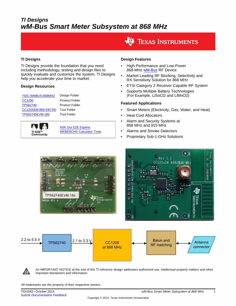
2.1 to 3.3 VCC1200
at 868 MHz
Balun and
RF matchingAntenna
connector
2.2 to 5.5 VTPS62740
TI DesignswM-Bus Smart Meter Subsystem at 868 MHz
TI Designs Design FeaturesTI Designs provide the foundation that you need • High-Performance and Low-Powerincluding methodology, testing and design files to 868-MHz wM-Bus RF Devicequickly evaluate and customize the system. TI Designs • Market Leading RF Blocking, Selectivity andhelp you accelerate your time to market. RX Sensitivity Solution for 868 MHz
• ETSI Category 2 Receiver Capable RF SystemDesign Resources• Supports Multiple Battery Technologies
Design FolderTIDC-WMBUS-868MHZ (For Example, LiSoCl2 and LiMnO2)CC1200 Product Folder
Featured ApplicationsTPS62740 Product FolderCC120XEM-868-930-RD Tool Folder • Smart Meters (Electricity, Gas, Water, and Heat)TPS62740EVM-186 Tool Folder • Heat Cost Allocators
• Alarm and Security Systems at868 MHz and 915 MHzASK Our E2E Experts
• Alarms and Smoke DetectorsWEBENCH® Calculator Tools
• Proprietary Sub-1-GHz Solutions
An IMPORTANT NOTICE at the end of this TI reference design addresses authorized use, intellectual property matters and otherimportant disclaimers and information.
All trademarks are the property of their respective owners.
1TIDU582–October 2014 wM-Bus Smart Meter Subsystem at 868 MHzSubmit Documentation Feedback
Copyright © 2014, Texas Instruments Incorporated
Introduction www.ti.com
1 IntroductionThis reference design describes an ETSI Cat. 2 receiver-capable RF subsystem for smart meters andsub-meters, fully compliant with the most popular wM-Bus S-, T-, and C-Modes at 868 MHz as perEN13757-4:2014.
The CC1200 transceiver device delivers market leading blocking, selectivity, and RX sensitivity numbersin wM-Bus applications such as bi-directional flow meters, e-meters and heat cost allocators. This cost-optimized design handles the worst case frequency offset of ±60ppm in S2-Mode by utilizing a low-costXTAL component. This design needs neither an external SAW filter nor a costly TCXO component to meetthe specification of the wM-Bus modes at 868 MHz.
Adding TPS62740, an ultra-low Iq DC-DC device with dynamically adjustable output voltage, enables anew level of optimization of the design's power consumption, significantly extending the battery lifetime.
2 Key System SpecificationsThe CC1200 is a transceiver device with excellent blocking, selectivity, and receiver (RX) sensitivity in thesupported ISM bands at 164 to 190 MHz, 410 to 475 MHz, and 820 to 950 MHz. This design has beenoptimized for operation in the ETSI ISM 868-MHz band, where the wM-Bus communication protocol isused. CC1200 radio operates from 2.0 to 3.6 V (up to 3.9 V as the absolute maximum are allowed), thetransmit current for 14 dBm of transmitter (TX) power (conducted measurement) is typically 46 mA at a3.0-V supply. The input supply voltage coming from the battery or power management system should beabove 2.1 V to guarantee best RF performance of the CC1200 radio. Supported data rates are from0 to 1250 kbps, and 2-FSK, 2-GFSK, 4-FSK, 4-GFSK, MSK, and OOK modulation formats are available.Either 2-FSK or 2-GFSK modulation formats are required to comply with the most popular wM-Bus modesat 868 MHz, called S2, T2, and C2.
The CC1200EM-868-930 has been optimized for the 868-MHz band: this design has no SAW filter and noTCXO components used. Still, adding an external SAW component is possible and a good practice inmany applications.
In addition to low-cost XTAL devices, the CC1200 also supports TCXO components for applications thatmandate the highest-possible frequency accuracy over temperature and lifetime, such as smart utilitymeters.
The TPS62740 is the industry’s first step-down converter featuring a 360-nA quiescent current (typical)and operating with a tiny 2.2-μH inductor and a 10-μF output capacitor with user selectable output voltage.Four VSEL pins that can be connected to a microcontroller (MCU) device allow dynamic voltageadjustment in the range from 1.8 to 3.3 V in 100-mV steps. The maximum input voltage of up to 5.5 Venables operation from a USB port and thin-film solar modules. The TPS62740 is available in a small12-pin 2×3 mm2 WSON package and supports a total solutions size of 31 mm2.
For highest power efficiency and lowest energy consumption, the TPS62740 output voltage is set to 2.1 Vwith the help of the VSEL pins.
Table 1. TPS6274x Device Options
OUTPUT VOLTAGE OUTPUT CURRENTTA PART NUMBER PACKAGE MARKINGSETTING VSEL 1 TO 4 (mA)TPS62740 1.8 to 3.3 V in 100-mV steps 300 mA 62740
–40°C to 85°C TPS62741 (1) 1.3 to 2.8 V in 100-mV steps 300 mA -/-TPS62742 1.8 to 3.3 V in 100-mV steps 400 mA 62742
(1) Device option, contact TI for more details
The operating ambient temperature for both CC1200 and TPS62740 is TA = –40°C to 85°C.
2 wM-Bus Smart Meter Subsystem at 868 MHz TIDU582–October 2014Submit Documentation Feedback
Copyright © 2014, Texas Instruments Incorporated
www.ti.com System Description
3 System DescriptionThe CC1200 device is optimized towards wideband applications but can also cover narrowband solutionsdown to 12.5-kHz channels.
Using a supply voltage of up to 3.6 V delivers excellent RF results. However, the drawback is increasedpower loss in the internal LDOs of the CC1120. To reduce these losses and extend the battery life in suchan RF system, TI recommends using the lowest-possible supply voltage for each operation mode. So thesupply voltage can vary between receive, transmit and sleep (power-down) operation of CC1200 and theMCU (such as MSP430). Another constraint is that the supply voltage must be the same for both MCUsrunning the RF communication protocol (for example, the wM-Bus S2-, T2-, or C2-Mode RF stack) and theCC1200 radio. This constraint helps avoid voltage level issues on the SPI and on the control signalsbetween the radio and the MCU.
All these considerations lead to the choice of TPS62740 with its dynamic output voltage selectioncapability and ultra-low Iq current of only 360 nA.
Depending on the application’s duty cycle (for example, how often a system must transmit or receive dataper day, for how long, and at which transmit power level) a different power scheme will be most efficient.In wM-Bus 868-MHz applications, such as smart utility meters and heat cost allocators, the transmitoperations may occur from six times per day up to over several hundred times per day with a maximumERP of 14 dBm (or 25 mW).
Knowing the duty cycle of the transmission and reception activity, it is easy to calculate the full systempower budget (current consumed by CC1200 × operational time × voltage level as well as the energydrawn in sleep mode) and find out the most energy efficient option.
This option could be either to shut down (power-off) completely the CC1200 or put it into low-power (sleepstate) with data retention. The power-up and initialization procedure of the CC1200 takes just a fewmilliseconds and has to be repeated every time the device starts from shut-down. Alternatively, using thesleep mode with retention (typical value is 120 nA) might be the more effective when a transmission orreception activity happens more often.
The combination of the TPS62740+CC1200 radio delivers a RF solution, which is market leading in termsof both wM-Bus 868-MHz performance and very low-power consumption. This design has been developedto meet and exceed the requirements of all wM-Bus systems at 868 MHz, which are already very popularin Europe for smart flow and electricity meters as well as for heat cost allocators.
3TIDU582–October 2014 wM-Bus Smart Meter Subsystem at 868 MHzSubmit Documentation Feedback
Copyright © 2014, Texas Instruments Incorporated
BIAS
RB
IAS
XO
SC
_Q
1
XO
SC
_Q
2
XOSC
LNA
0
90
FREQ
SYNTH
ADC
ADC
DE
MO
DU
LA
TO
R
PA
CK
ET
HA
ND
LE
R
RX
FIF
O
MO
DU
LA
TO
R
TX
FIF
O
RADIO CONTROL & POWER MANAGEMENT
LNA_P
LNA_N
PA
EX
T_
XO
SC
PA
LFC
1
CS_N
SI
SO (GPIO0)
SCLK
GPIO2
GPIO1
GPIO3
DIG
ITA
LIN
TE
RFA
CE
TO
MC
U
LFC
0
CC120x
MARC
Main Radio Control unit
Ultra low power 16 bit
MCU
256 byte
FIFO RAM
buffer
4 kbyte
ROM
RF and DSP frontend
Packet handler
and FIFO controlConfiguration and
status registers
eWOR
Enhanced ultra low power
Wake On Radio timer
SPI
Serial configuration
and data interface
Interrupt and
IO handlerSystem bus
PA out
LNA_P
LNA_N
90 dB dynamic
range ADC
90 dB dynamic
range ADC
High linearity
LNA
+16 dBm high
efficiency PA
Ch
an
ne
l
filte
r
XOSC
Co
rdic
AGC
Automatic Gain Control, 60dB VGA range
RSSI measurements and carrier sense detection
Highly flexible FSK / OOK
demodulator
(optional bit clock)
(optional low jitter serial
data output for legacy
protocols)
Data interface with
signal chain access
XOSC_Q1
XOSC_Q2
Ultra low power 40 kHz
auto-calibrated RC oscillator(optional 40 kHz
clock input)
CSn (chip select)
SI (serial input)
SO (serial output)
SCLK (serial clock)
(optional GPIO3/2/0)
Mo
du
lato
r
Fully integrated fractional-N
frequency synthesizer
Output power ramping and OOK / ASK modulation
IF amp
IF amp
(optional auto detected
external XOSC / TCXO)
(optional GPIO for
antenna diversity)
I
Q
Battery sensor /
temp sensor
Power on reset
AES-128
accelerator
System Description www.ti.com
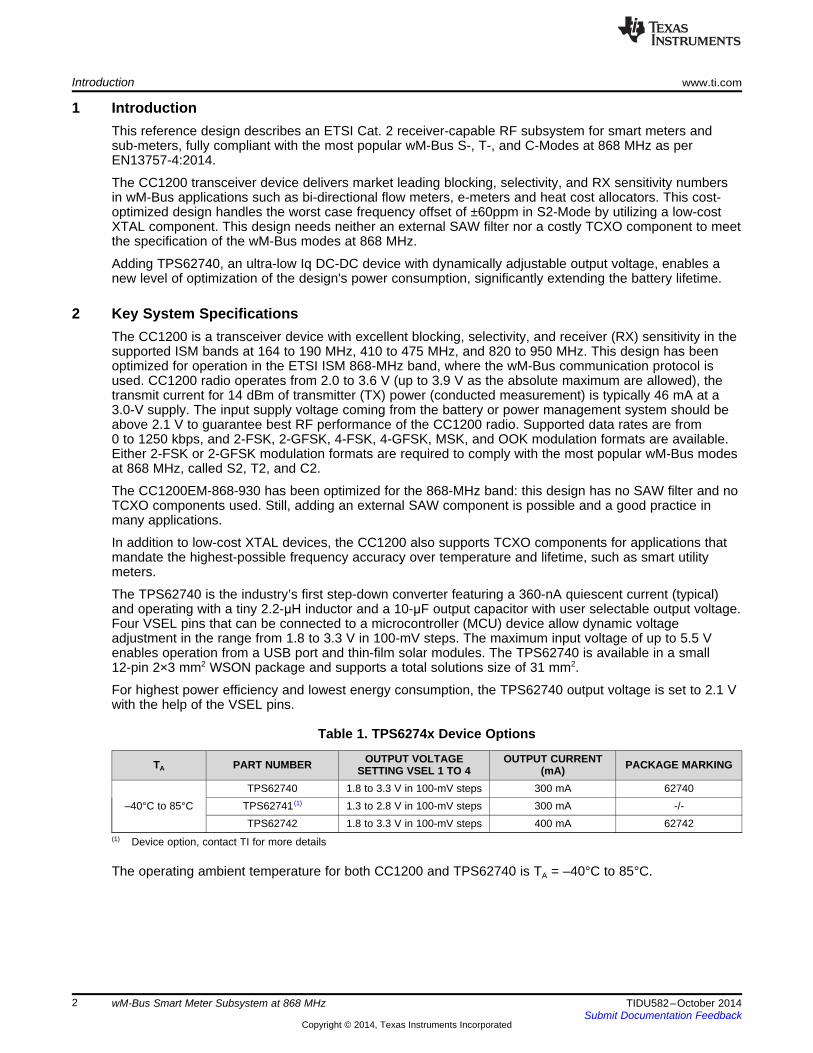
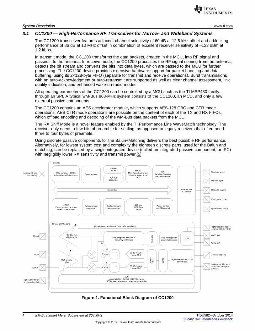
3.1 CC1200 — High-Performance RF Transceiver for Narrow- and Wideband SystemsThe CC1200 transceiver features adjacent channel selectivity of 60 dB at 12.5 kHz offset and a blockingperformance of 86 dB at 10 MHz offset in combination of excellent receiver sensitivity of –123 dBm at1.2 kbps.
In transmit mode, the CC1200 transforms the data packets, created in the MCU, into RF signal andpasses it to the antenna. In receive mode, the CC1200 processes the RF signal coming from the antenna,detects the bit stream and converts the bits into data bytes, which are passed to the MCU for furtherprocessing. The CC1200 device provides extensive hardware support for packet handling and databuffering, using its 2×128-byte FIFO (separate for transmit and receive operations). Burst transmissionswith an auto-acknowledgment or auto-retransmit are supported as well as clear channel assessment, linkquality indication, and enhanced wake-on-radio modes.
All operating parameters of the CC1200 can be controlled by a MCU such as the TI MSP430 familythrough an SPI. A typical wM-Bus 868-MHz system consists of the CC1200, an MCU, and only a fewexternal passive components.
The CC1200 contains an AES accelerator module, which supports AES-128 CBC and CTR modeoperations. AES CTR mode operations are possible on the content of each of the TX and RX FIFOs,which offload encoding and decoding of the wM-Bus data packets from the MCU.
The RX Sniff Mode is a novel feature enabled by the TI Performance Line WaveMatch technology. Thereceiver only needs a few bits of preamble for settling, as opposed to legacy receivers that often needthree to four bytes of preamble.
Using discrete passive components for the Balun+Matching delivers the best possible RF performance.Alternatively, for lowest system cost and complexity the eighteen discrete parts, used for the Balun andmatching, can be replaced by a single integrated device (called an integrated passive component, or IPC)with negligibly lower RX sensitivity and transmit power.[5]
Figure 1. Functional Block Diagram of CC1200
4 wM-Bus Smart Meter Subsystem at 868 MHz TIDU582–October 2014Submit Documentation Feedback
Copyright © 2014, Texas Instruments Incorporated
UVLO
EN
Gate DriverAnti
Shoot-Through
CurrentLimit Comparator
SW
LimitHigh Side
VIN
GND
PMOS
NMOS
PG
PG Comp
VTH_UVLO
VIN
UVLOComp
Softstart
ControlLogic
VOUT
VFB
MainComparator
Direct Control& Compensation
Erroramplifier
Min. On
Min. OFF
VIN
VOUT
Timer
DCSControl
Current
Limit Comparator
LimitLow Side
Power Stage
UVLO
Slew RateControl
VOUT
Discharge
Load Switch
EN
UVLO
CTRL
LOAD
Internalfeedback
dividernetwork*
VSEL 1
VSEL 2
VSEL 3
VSEL 4
Ultra Low PowerReference V = 1.2VREF
VTH_100
VIN
Auto 100% ModeComp
100%Mode
VTH_PG
V
DischargeOUT
VFB
UVLO
EN
EN
CTRL
VOUT
* typical 50MW
VREF
VFB
www.ti.com System Description
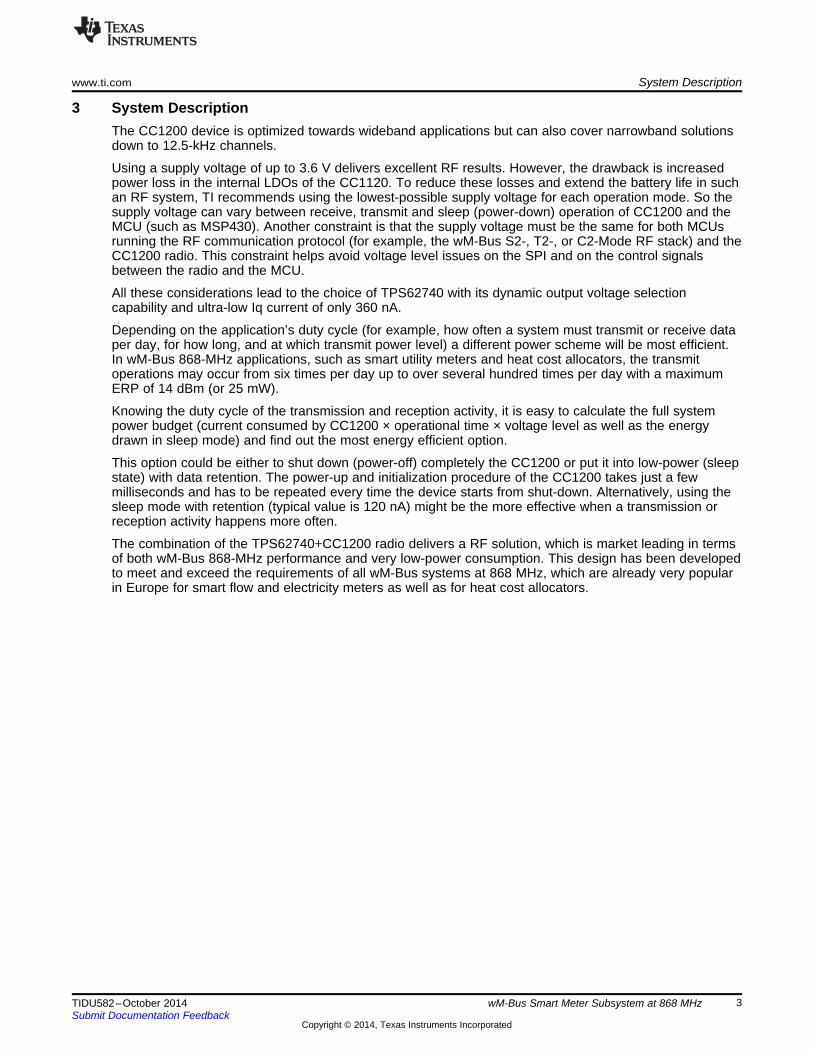
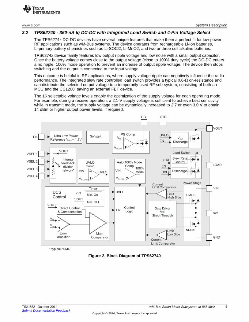
3.2 TPS62740 - 360-nA Iq DC-DC with Integrated Load Switch and 4-Pin Voltage SelectThe TPS6274x DC-DC devices have several unique features that make them a perfect fit for low-powerRF applications such as wM-Bus systems. The device operates from rechargeable Li-Ion batteries,Li-primary battery chemistries such as Li-SOCl2, Li-MnO2, and two or three cell alkaline batteries.
TPS6274x device family features low output ripple voltage and low noise with a small output capacitor.Once the battery voltage comes close to the output voltage (close to 100% duty cycle) the DC-DC entersa no ripple, 100% mode operation to prevent an increase of output ripple voltage. The device then stopsswitching and the output is connected to the input voltage.
This outcome is helpful in RF applications, where supply voltage ripple can negatively influence the radioperformance. The integrated slew rate controlled load switch provides a typical 0.6-Ω on-resistance andcan distribute the selected output voltage to a temporarily used RF sub-system, consisting of both anMCU and the CC1200, saving an external FET device.
The 16 selectable voltage levels enable the optimization of the supply voltage for each operating mode.For example, during a receive operation, a 2.1-V supply voltage is sufficient to achieve best sensitivitywhile in transmit mode, the supply voltage can be dynamically increased to 2.7 or even 3.0 V to obtain14 dBm or higher output power levels, if required.
Figure 2. Block Diagram of TPS62740
5TIDU582–October 2014 wM-Bus Smart Meter Subsystem at 868 MHzSubmit Documentation Feedback
Copyright © 2014, Texas Instruments Incorporated
2.1 to 3.3 VCC1200
at 868 MHz
Balun and
RF matchingAntenna
connector
2.2 to 5.5 VTPS62740
Block Diagram www.ti.com
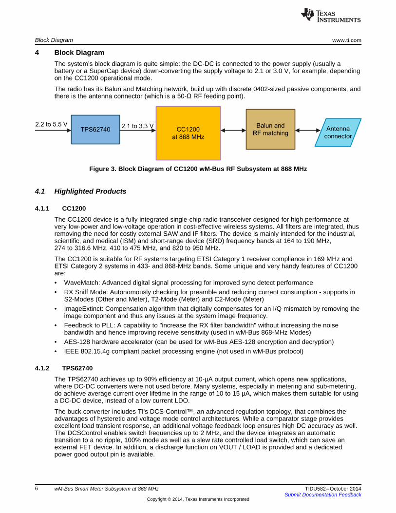
4 Block DiagramThe system’s block diagram is quite simple: the DC-DC is connected to the power supply (usually abattery or a SuperCap device) down-converting the supply voltage to 2.1 or 3.0 V, for example, dependingon the CC1200 operational mode.
The radio has its Balun and Matching network, build up with discrete 0402-sized passive components, andthere is the antenna connector (which is a 50-Ω RF feeding point).
Figure 3. Block Diagram of CC1200 wM-Bus RF Subsystem at 868 MHz
4.1 Highlighted Products
4.1.1 CC1200The CC1200 device is a fully integrated single-chip radio transceiver designed for high performance atvery low-power and low-voltage operation in cost-effective wireless systems. All filters are integrated, thusremoving the need for costly external SAW and IF filters. The device is mainly intended for the industrial,scientific, and medical (ISM) and short-range device (SRD) frequency bands at 164 to 190 MHz,274 to 316.6 MHz, 410 to 475 MHz, and 820 to 950 MHz.
The CC1200 is suitable for RF systems targeting ETSI Category 1 receiver compliance in 169 MHz andETSI Category 2 systems in 433- and 868-MHz bands. Some unique and very handy features of CC1200are:• WaveMatch: Advanced digital signal processing for improved sync detect performance• RX Sniff Mode: Autonomously checking for preamble and reducing current consumption - supports in
S2-Modes (Other and Meter), T2-Mode (Meter) and C2-Mode (Meter)• ImageExtinct: Compensation algorithm that digitally compensates for an I/Q mismatch by removing the
image component and thus any issues at the system image frequency.• Feedback to PLL: A capability to "increase the RX filter bandwidth" without increasing the noise
bandwidth and hence improving receive sensitivity (used in wM-Bus 868-MHz Modes)• AES-128 hardware accelerator (can be used for wM-Bus AES-128 encryption and decryption)• IEEE 802.15.4g compliant packet processing engine (not used in wM-Bus protocol)
4.1.2 TPS62740The TPS62740 achieves up to 90% efficiency at 10-µA output current, which opens new applications,where DC-DC converters were not used before. Many systems, especially in metering and sub-metering,do achieve average current over lifetime in the range of 10 to 15 µA, which makes them suitable for usinga DC-DC device, instead of a low current LDO.
The buck converter includes TI's DCS-Control™, an advanced regulation topology, that combines theadvantages of hysteretic and voltage mode control architectures. While a comparator stage providesexcellent load transient response, an additional voltage feedback loop ensures high DC accuracy as well.The DCSControl enables switch frequencies up to 2 MHz, and the device integrates an automatictransition to a no ripple, 100% mode as well as a slew rate controlled load switch, which can save anexternal FET device. In addition, a discharge function on VOUT / LOAD is provided and a dedicatedpower good output pin is available.
6 wM-Bus Smart Meter Subsystem at 868 MHz TIDU582–October 2014Submit Documentation Feedback
Copyright © 2014, Texas Instruments Incorporated
www.ti.com System Design Theory
5 System Design TheorySeveral considerations were taken into account when defining this RF subsystem. The main focus was toget the best RF performance (RX sensitivity and blocking parameters) for wM-Bus 868-MHz modes,lowest system cost, and highest power efficiency. As the TX power level of CC1200 depends on thesupply voltage, it is a good practice to use different voltage levels for RX and TX operations, which ispossible with TPS62740. While optimal receive performance requires only a 2.1-V supply voltage, transmitoperation at 14 dBm needs a 2.7-V or higher voltage supply.
5.1 Power EfficiencyTPS62740 has been selected as it can dynamically adjust the output voltage level, making it a perfect fitfor low-power metering systems (for example wM-Bus enabled smart utility meters) or sub-meteringdevices (such as a heat cost allocator, or HCA). The optimal supply range for CC1200 between 2.1 V(highest energy savings) and 3.3 V (highest TX power levels) can be now fully supported with a singleDC-DC component, the TPS62740, and controlled through signal lines by the host MCU(such as MSP430).
5.2 RF Performance at 868 MHz (ETSI Cat. 2 Receiver Capable)CC1200 easily achieves ETSI Category 2 receiver category compliance; optimized register settings forbest RX sensitivity for each of the wM-Bus modes S2 (same as T2 for a Meter device) and C2 (for a Meterdevice) are provided with this design. Main focus is on the receive performance under all possibleparameter variations (or worst case), as this is the most challenging part for any wM-Bus system.
In this design guide, Meter Mode means the wM-Bus RX performance that needs to be supported by awM-Bus Meter device (for example, a smart utility Meter or HCA). The wM-Bus Other Mode, or thefunctionality required to implement a data collector system, is not analyzed here. Nevertheless, theCC1200 radio is also supporting C2-Other and T2-Other Modes and can be used in wM-Bus enabled datacollectors or mobile reader devices collecting metering data.
The CC1200 has been tested in the same RF test setup as CC1120EM-868 boards, documented in TI’swM-Bus application note.[4] The results for CC1200 RX sensitivity and the PER plots in Section 8.3 are in-line with that application note, proving also that the CC1200 is an equally capable wM-Bus device withmarket leading RF performance.
The transmit parameters for all wM-Bus Modes in 169-, 433-, or 868-MHz ISM bands, are derived usingthe SmartRF™ 7 Studio and the specific wM-Bus transmitter RF parameters as defined in the wM-BusStandard Document.[3]
5.3 System CostIn high-volume rollouts of 868-MHz RF systems in Europe, the full system cost as well as the bill ofmaterials (BOM) cost are of utmost importance. CC1200-based designs are leading not only in RFperformance but also in terms of system cost, as they can use any of two pin-compatible IPC products fora single-chip Balun+Matching, reducing handling and logistics costs and drastically simplifying the systemlayout.[5]
The “Feedback-to-PLL” is a powerful feature in the CC1200, which eases the XTAL specifications andtolerates larger frequency offset between transmitter and receiver units in the field deployment.
7TIDU582–October 2014 wM-Bus Smart Meter Subsystem at 868 MHzSubmit Documentation Feedback
Copyright © 2014, Texas Instruments Incorporated
Getting Started Hardware www.ti.com
6 Getting Started HardwareThe test hardware comprises three different hardware boards: one TRXEB board from the CC1200DK, theCC1200EM868-930 Rev1.1 board, and the TPS62740EVM-186. For the RF performance tests, twoCC1200EM868-930 Rev1.1 boards were measured by connecting a cable from the R&S® RF signalgenerator to the SMA antenna connector. All three boards together were used to measure currents independence of the TX output power under control of the TI SmartRF 7 Studio software.[11]
The RX Sniff Mode code example requires IAR Workbench for MSP430; the reported currentmeasurements apply for the combination of the TRXEB+CC1200EM868-930 board with and withoutTPS62740. The C-code examples can be easily ported to any other code development tools, such as TI’sCode Composer Studio™ (CCS) or GCC.
8 wM-Bus Smart Meter Subsystem at 868 MHz TIDU582–October 2014Submit Documentation Feedback
Copyright © 2014, Texas Instruments Incorporated
www.ti.com Getting Started Hardware
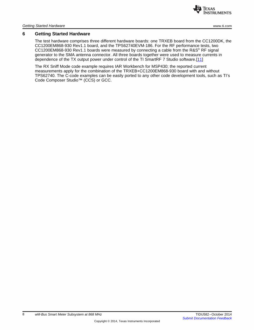
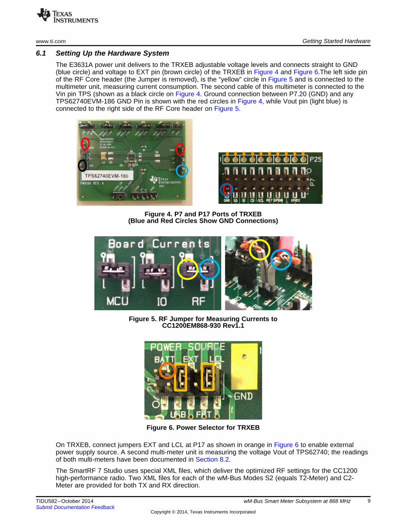
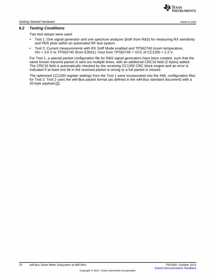
6.1 Setting Up the Hardware SystemThe E3631A power unit delivers to the TRXEB adjustable voltage levels and connects straight to GND(blue circle) and voltage to EXT pin (brown circle) of the TRXEB in Figure 4 and Figure 6.The left side pinof the RF Core header (the Jumper is removed), is the “yellow” circle in Figure 5 and is connected to themultimeter unit, measuring current consumption. The second cable of this multimeter is connected to theVin pin TPS (shown as a black circle on Figure 4. Ground connection between P7.20 (GND) and anyTPS62740EVM-186 GND Pin is shown with the red circles in Figure 4, while Vout pin (light blue) isconnected to the right side of the RF Core header on Figure 5.
Figure 4. P7 and P17 Ports of TRXEB(Blue and Red Circles Show GND Connections)
Figure 5. RF Jumper for Measuring Currents toCC1200EM868-930 Rev1.1
Figure 6. Power Selector for TRXEB
On TRXEB, connect jumpers EXT and LCL at P17 as shown in orange in Figure 6 to enable externalpower supply source. A second multi-meter unit is measuring the voltage Vout of TPS62740; the readingsof both multi-meters have been documented in Section 8.2.
The SmartRF 7 Studio uses special XML files, which deliver the optimized RF settings for the CC1200high-performance radio. Two XML files for each of the wM-Bus Modes S2 (equals T2-Meter) and C2-Meter are provided for both TX and RX direction.
9TIDU582–October 2014 wM-Bus Smart Meter Subsystem at 868 MHzSubmit Documentation Feedback
Copyright © 2014, Texas Instruments Incorporated
Getting Started Hardware www.ti.com
6.2 Testing ConditionsTwo test setups were used:• Test 1: One signal generator and one spectrum analyzer (both from R&S) for measuring RX sensitivity
and PER plots within an automated RF test system.• Test 2: Current measurements with RX Sniff Mode enabled and TPS62740 (room temperature,
Vin = 3.6 V to TPS62740 (from E3631); Vout from TPS62740 = VCC of CC1200 = 2.3 V.
For Test 1, a special packet configuration file for R&S signal generators have been created, such that thesame known transmit packet is sent out multiple times, with an additional CRC16 field (2 bytes) added.The CRC16 field is automatically checked by the receiving CC1200 CRC block engine and an error isindicated if at least one bit in the received packet is wrong or a full packet is missed.
The optimized CC1200 register settings from the Test 1 were incorporated into the XML configuration filesfor Test 2. Test 2 uses the wM-Bus packet format (as defined in the wM-Bus standard document) with a20-byte payload.[3]
10 wM-Bus Smart Meter Subsystem at 868 MHz TIDU582–October 2014Submit Documentation Feedback
Copyright © 2014, Texas Instruments Incorporated
www.ti.com Getting Started Firmware
7 Getting Started FirmwareThere are two different options to test the CC1200EM performance: the TRXEB embedded firmware forSmartRF 7 or a “custom” code for S2- and C2-Meter Modes with RX Sniff functionality support, createdbased on the RX Sniff Mode application report.[7]
Additionally, Excel files for calculating the RX Sniff current consumption are provided for S2-and C2-Modes, using the corresponding optimized wM-Bus register settings.
7.1 SmartRF 7 Studio FilesThe DUT board is controlled through SmartRF 7 with specific configuration files for S2 and C2-Modes,running on a Windows® PC and connected thru a USB cable to the TRXEB. The SmartRF 7 Studio GUIreports correct and missing or wrong packets and calculates the packet error rate (PER) automatically.The embedded TRXEB firmware is enabled by setting the DIP switch to “USB Mode Smart RF”.
7.2 Test FramesThe wM-Bus data packet is created according to the different RF parameters for S2- and C2-MeterModes, as in Table 2:
Table 2. Definition of S2- and C2-Meter Packet Formats[3]
PREAMBLE n SYNC WORD POSTAMBLE N LINKS-Mode, shortn*(01) 15 ≤ n 00 0111 0110 1001 0110 n*(01) 2 ≤ n ≤ 4 preamble
0101010000111101 0101010011001101 (frame format A) C2-Moden*(01) 16 = n NA NA0101010000111101 0101010000111101 (frame format B) Meter
The conversion into text format (hexadecimal):
PREAMBLE SYNC PACKET DATA COMMENT0x55 55 55 54 76 96 20 bytes of payload FF if S2-Mode (=T2-Mode Meter)0x55 55 55 54 3D 54 3D 21 bytes of payload -- if C2-Mode Meter
11TIDU582–October 2014 wM-Bus Smart Meter Subsystem at 868 MHzSubmit Documentation Feedback
Copyright © 2014, Texas Instruments Incorporated
Getting Started Firmware www.ti.com
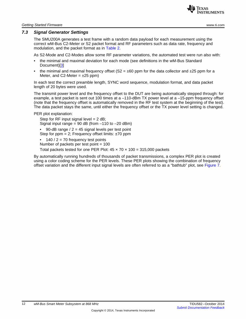
7.3 Signal Generator SettingsThe SMU200A generates a test frame with a random data payload for each measurement using thecorrect wM-Bus C2-Meter or S2 packet format and RF parameters such as data rate, frequency andmodulation, and the packet format as in Table 2.
As S2-Mode and C2-Modes allow some RF parameter variations, the automated test were run also with:• the minimal and maximal deviation for each mode (see definitions in the wM-Bus Standard
Document)[3]• the minimal and maximal frequency offset (S2 = ±60 ppm for the data collector and ±25 ppm for a
Meter, and C2-Meter = ±25 ppm)
In each test the correct preamble length, SYNC word sequence, modulation format, and data packetlength of 20 bytes were used.
The transmit power level and the frequency offset to the DUT are being automatically stepped through: forexample, a test packet is sent out 100 times at a –110-dBm TX power level at a –15-ppm frequency offset(note that the frequency offset is automatically removed in the RF test system at the beginning of the test).The data packet stays the same, until either the frequency offset or the TX power level setting is changed.
PER plot explanation:Step for RF input signal level = 2 dB;Signal input range = 90 dB (from –110 to –20 dBm)• 90-dB range / 2 = 45 signal levels per test pointStep for ppm = 2; Frequency offset limits: ±70 ppm• 140 / 2 = 70 frequency test pointsNumber of packets per test point = 100Total packets tested for one PER Plot: 45 × 70 × 100 = 315,000 packets
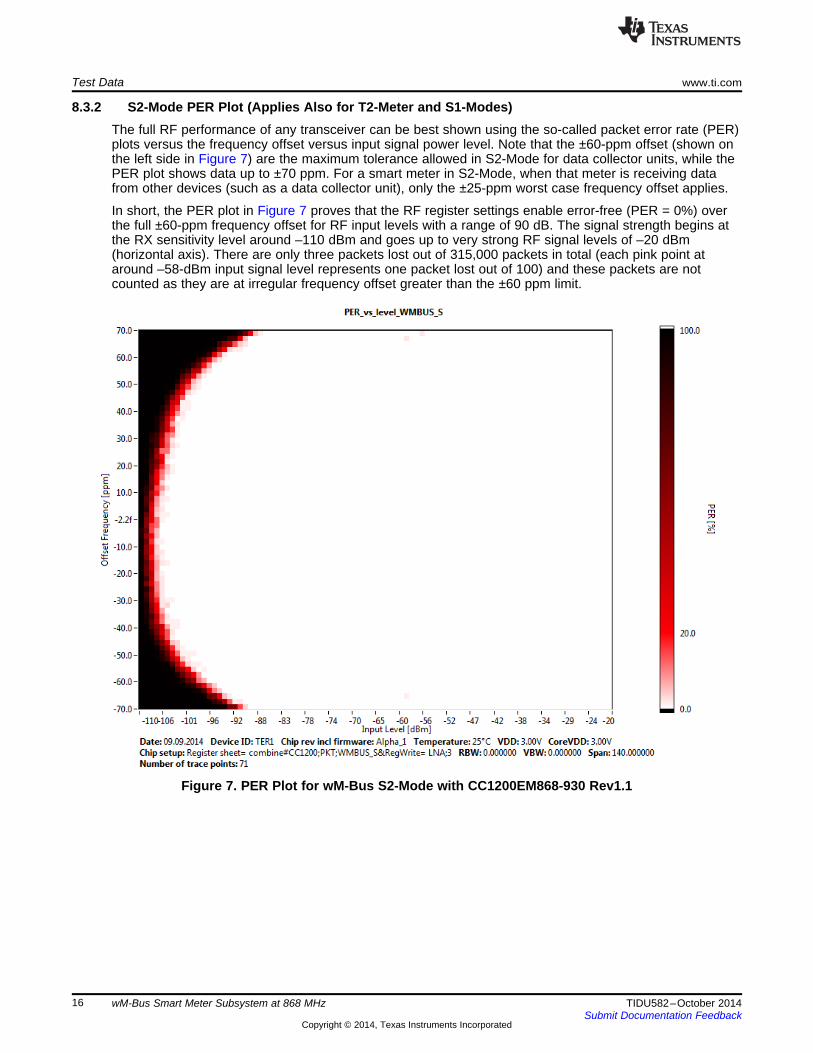
By automatically running hundreds of thousands of packet transmissions, a complex PER plot is createdusing a color coding scheme for the PER levels. These PER plots showing the combination of frequencyoffset variation and the different input signal levels are often referred to as a “bathtub” plot, see Figure 7.
12 wM-Bus Smart Meter Subsystem at 868 MHz TIDU582–October 2014Submit Documentation Feedback
Copyright © 2014, Texas Instruments Incorporated
www.ti.com Test Data
8 Test DataThe automated performance numbers was tested on two regular CC1200EM868-930Rev1.1 boards, nohardware modifications have been done. The boards have no SAW filter and no TCXO; instead, a low-cost 10-ppm XTAL is used as a reference clock source for the CC1200 device. The TPS62740 DC-DCdevice was not used in the RX sensitivity tests and PER plots. RF signals are always measured at theantenna connector at room temperature.
8.1 TX CurrentFor this test, unmodulated TX carrier has been generated through SmartRF 7 at 868.3 MHz, TPS62740Vin = 3.6 V, and Vout = 2.1 V.
Table 3. TX Current (Unmodulated Carrier) at 868.3 MHz (S2-Mode Frequency) and 3.6 Vin
SMARTRF 7 STUDIO Vin TO TPS62740 = 3.6 V, Vout = 2.1 V;R&S FSIQ7 READING (dBm)TX SETTING (dBm) TPS INPUT CURRENT (mA)14 11.93 25.8213 11.33 23.8810 9.29 20.386 5.44 16.760 –0.41 15.87–6 –6.4 12.32–12 –12.31 11.43–24 –25.02 10.35–40 –43.01 9.58
Comparison: CC1200EM uses 36 mA at 10 dBm TX power and a 3-V supply (see the CC1200datasheet; no TPS62740 used).[1]
The TX current has additional current consumption numbers for 3.3-V and 3.0-V external power supplies,and TPS62740 Vout = 2.1 V.
Table 4. TX Current versus Vin Level versus TX Power Level forUnmodulated TX Carrier (at 868.3 MHz)
SMARTRF 7 STUDIO Vin to TPS62740 = 3.3 V; Vin to TPS62740 = 3.0 V;R&S FSIQ7 READING (dBm)TX SETTING (dBm) TPS INPUT CURRENT (mA) TPS INPUT CURRENT (mA)14 11.93 28.89 32.3613 11.33 26.78 30.0510 9.29 23 25.896 5.44 19.03 21.560 –0.41 15.89 18.12–6 –6.4 14.21 16.28
–12 –12.31 13.24 15.22–24 –25.02 12.07 13.95–40 –43.01 11.23 13.03
Summary: Due to the >90% DC-DC conversion efficiency, the higher the Vin voltage the lower the currentconsumption of the CC1200 is.
Best results are achieved for 3.6-V voltage, being typical for LiSoCL2 primary batteries, which are quiteoften used in Metering applications. But also with 3.0-V input voltage, common for LiMnO2 batteries, theTPS62740 can deliver power savings, as shown in the far-right column of Table 4.
13TIDU582–October 2014 wM-Bus Smart Meter Subsystem at 868 MHzSubmit Documentation Feedback
Copyright © 2014, Texas Instruments Incorporated
Test Data www.ti.com
8.2 RX CurrentExternal power supply is 3.6 V. The boards used are TPS62740EVM-186, TRXEB, and CC1200EM868-930Rev1.1; TPS62740 Vin = 3.6 V and Vout = 2.3 V. The carrier sense is 1 dB below the sensitivity limit(CS = –109 dB) for both S2 and C2-Mode (Meter).
Table 5. RX Current versus Vin
DATA RATE MEASURED CURRENT IN mA COMMENTS2-Mode and T2-Mode (Meter) 8.52 mA 998 of 1000 data packetsS2-Mode and T2-Mode (Meter) 7.45 mA No data packets
C2-Mode (Meter) 6.43 mA 1000 of 1000 data packetsC2-Mode (Meter) 7.42 mA No data packets
Comparison: RX current = 23 mA at 3.3 V (USB power to TRXEB)
NOTE: The RX Sniff Mode current is highly dependant on the RF noise in the channel (wM-Busfrequency) used. The measured current also depends on the inactivity time period betweeneach wM-Bus packet (bursts of 250 packets were used).
8.3 RX Performance in S2- and T2-Modes for Meter DeviceThe wM-Bus S2-Mode with 30 bits of preamble (which is also used in T2-Mode response to the Meter)has sufficient time for CC1200 to autonomously duty cycle the receiver while searching for a preamble.Therefore, the RX Sniff Mode can be used, offering dramatically reduced average current withoutcompromising the RF performance. The RX Sniff Mode is enabled by using the eWOR timer together withthe RX termination based on carrier sense (CS).
Packet format: preamble (n = 15) × (01) + sync word “000111011010010110” + P byte payload + CRC16;with n ≥ 15 for the sub-Mode S2 (short header).
Table 6 summarizes the test conditions used:
Table 6. S-Mode Test Conditions
PARAMETER VALUETX/RX centre frequency (MHz) 868.3
Modulation 2-FSKFrequency deviation (kHz) ±50 (min. ±40; max. ±80)
Chip rate (kcps) 32.768 ±2%RX filter bandwidth (kHz) 208.333
NOTE: The long preamble used in S1 Mode is supported by CC1200 but not analyzed in this designguide (S2-Mode with the short preamble is much more challenging to support). Typically,numbers for S1-Mode will be a bit better than for S2-Mode because of the very longpreamble of 69.75 bytes, which allows a very reliable SYNC detection in the receiver andreduces the PER.
14 wM-Bus Smart Meter Subsystem at 868 MHz TIDU582–October 2014Submit Documentation Feedback
Copyright © 2014, Texas Instruments Incorporated
www.ti.com Test Data
8.3.1 S2-Mode RX SensitivityThe summary of S2-Mode sensitivity performance of CC1200 under all conditions is in Table 7, achievingmarket leading –109 dBm at 80% PER and –107.5 dBm at 20% PER.
Table 7. S2-Mode and T2-Meter Typical RX Sensitivity Numbers for CC1200
TYPICAL SENSITIVITY PARAMETER INFREQUENCY (MHz) PER (%) P = PAYLOAD BYTES(dBm) EN13757-4–109 80 20
–107.5 20 20–106.25 1 20
868.3 –107 20 20 Max Deviation = 80 kHz–106.75 20 20 Min Deviation = 40 kHz–107.5 20 20 Max. data rate = 32.768 +2%–107.5 20 20 Min. data rate = 32.768 –2%
NOTE: RX sensitivity numbers are measured conducted at the single antenna port with combinedTX/RX matching (and not at the CC1200 chip pin).
Summary: CC1200 exceeds the S2-, S1-m, and T2-Meter Mode (32.768 kcps) requirements, achievingmarket leading sensitivity of –109 dBm at 80% PER, which is 1.5 dB better than the nearest competitorsolution.
15TIDU582–October 2014 wM-Bus Smart Meter Subsystem at 868 MHzSubmit Documentation Feedback
Copyright © 2014, Texas Instruments Incorporated
Test Data www.ti.com
8.3.2 S2-Mode PER Plot (Applies Also for T2-Meter and S1-Modes)The full RF performance of any transceiver can be best shown using the so-called packet error rate (PER)plots versus the frequency offset versus input signal power level. Note that the ±60-ppm offset (shown onthe left side in Figure 7) are the maximum tolerance allowed in S2-Mode for data collector units, while thePER plot shows data up to ±70 ppm. For a smart meter in S2-Mode, when that meter is receiving datafrom other devices (such as a data collector unit), only the ±25-ppm worst case frequency offset applies.
In short, the PER plot in Figure 7 proves that the RF register settings enable error-free (PER = 0%) overthe full ±60-ppm frequency offset for RF input levels with a range of 90 dB. The signal strength begins atthe RX sensitivity level around –110 dBm and goes up to very strong RF signal levels of –20 dBm(horizontal axis). There are only three packets lost out of 315,000 packets in total (each pink point ataround –58-dBm input signal level represents one packet lost out of 100) and these packets are notcounted as they are at irregular frequency offset greater than the ±60 ppm limit.
Figure 7. PER Plot for wM-Bus S2-Mode with CC1200EM868-930 Rev1.1
16 wM-Bus Smart Meter Subsystem at 868 MHz TIDU582–October 2014Submit Documentation Feedback
Copyright © 2014, Texas Instruments Incorporated
www.ti.com Test Data
8.3.3 S2-Mode RX Sniff ModeFor the measurements in Table 8, both TPS62740EVM-186 and CC1200EM868-930 Rev1.1 were used(as described in Section 6.1) together with the TRXEB. The RX Sniff software example has been flashedonto one TRXEB, which is used as the receive unit. A second TRXEB board is programmed with the RXSniff code and is used as a wM-Bus packet generator, transmitting single or bursts of 250 wM-Buscompliant data packets. A CC1200EM868-930Rev1.0 board was used on the second TRXEB toimplement this transmitter function.
Table 8. Average RX Current Consumption in RX Sniff Mode in S2-Mode and T2-Mode Meter (ShortPreamble)
TRIGGERING ON TRIGGERING ON RSSIPREAMBLE TRIGGERING ON RSSI,DATA RATE RSSI (SMARTRF 7 WITH TPS62740BYTES NO DC-DCESTIMATED VALUE) (MEASURED)32.768 kcps 2FSK = S2-Mode Vout = 2.3 V7.93 mA (assumes 8.37 mA (measured in(Meter and Data Collector) = 3.75 8.61 mA (3.0 Vin)noise-free channel) office environment)T2-Mode (Meter) 6.83 mA (3.6 Vin)
8.4 RX Performance in C2-Mode for Meter DeviceIn C2-Mode, a data collector unit uses a 50-kbps data rate to transmit data to a wM-Bus Meter device,with four bytes preamble and four bytes of sync word. Therefore, the RX Sniff Mode can also be used in ameter while waiting for a wM-Bus data packet from the Other device.
Table 9. C2-Meter Mode Test Conditions
PARAMETER VALUETX and RX center frequency (MHz) 869.525
Modulation 2-GFSKFrequency deviation (kHz) ±25 (min.±18.75; max. ±31.25)
Chip rate (kcps) 50 ±100 ppmRX filter bandwidth (kHz) 104.167
8.4.1 C2-Mode RX SensitivityThe summary of C2-Mode sensitivity performance of CC1200 under all conditions is in Table 10:
Table 10. C2-Meter Mode Typical Sensitivity Numbers for CC1200
PARAMETER INFREQUENCY (MHz) TYPICAL SENSITIVITY (dBm) PER (%) P = PAYLOAD BYTES EN13757-4–110 80 20–108 20 20
869.525 –106.5 1 20–109.5 20 20 Max deviation = ±31.25 kHz–110.25 20 20 Min deviation = ±18.25 kHz
NOTE: RX sensitivity numbers are measured conducted at the single antenna port with combinedTX and RX matching (and not at the CC1200 chip pin).
Summary: CC1200 exceeds the C2-Meter Mode (50 kbps) requirements, achieving market leadingsensitivity of –110 dBm at 80% PER, which is 2 dB better than the nearest competitor solution.
17TIDU582–October 2014 wM-Bus Smart Meter Subsystem at 868 MHzSubmit Documentation Feedback
Copyright © 2014, Texas Instruments Incorporated
Test Data www.ti.com
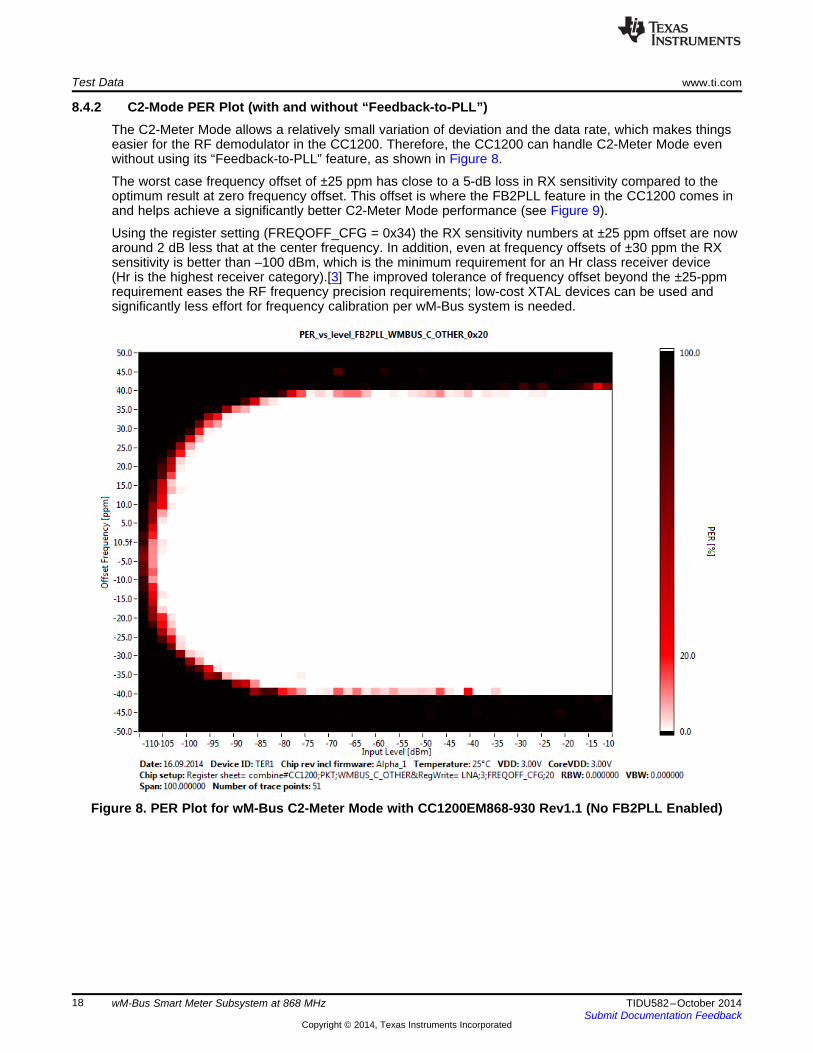
8.4.2 C2-Mode PER Plot (with and without “Feedback-to-PLL”)The C2-Meter Mode allows a relatively small variation of deviation and the data rate, which makes thingseasier for the RF demodulator in the CC1200. Therefore, the CC1200 can handle C2-Meter Mode evenwithout using its “Feedback-to-PLL” feature, as shown in Figure 8.
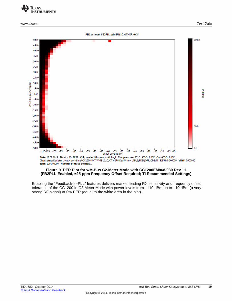
The worst case frequency offset of ±25 ppm has close to a 5-dB loss in RX sensitivity compared to theoptimum result at zero frequency offset. This offset is where the FB2PLL feature in the CC1200 comes inand helps achieve a significantly better C2-Meter Mode performance (see Figure 9).
Using the register setting (FREQOFF_CFG = 0x34) the RX sensitivity numbers at ±25 ppm offset are nowaround 2 dB less that at the center frequency. In addition, even at frequency offsets of ±30 ppm the RXsensitivity is better than –100 dBm, which is the minimum requirement for an Hr class receiver device(Hr is the highest receiver category).[3] The improved tolerance of frequency offset beyond the ±25-ppmrequirement eases the RF frequency precision requirements; low-cost XTAL devices can be used andsignificantly less effort for frequency calibration per wM-Bus system is needed.
Figure 8. PER Plot for wM-Bus C2-Meter Mode with CC1200EM868-930 Rev1.1 (No FB2PLL Enabled)
18 wM-Bus Smart Meter Subsystem at 868 MHz TIDU582–October 2014Submit Documentation Feedback
Copyright © 2014, Texas Instruments Incorporated
www.ti.com Test Data
Figure 9. PER Plot for wM-Bus C2-Meter Mode with CC1200EM868-930 Rev1.1(FB2PLL Enabled, ±25-ppm Frequency Offset Required; TI Recommended Settings)
Enabling the “Feedback-to-PLL” features delivers market leading RX sensitivity and frequency offsettolerance of the CC1200 in C2-Meter Mode with power levels from –110 dBm up to –10 dBm (a verystrong RF signal) at 0% PER (equal to the white area in the plot).
19TIDU582–October 2014 wM-Bus Smart Meter Subsystem at 868 MHzSubmit Documentation Feedback
Copyright © 2014, Texas Instruments Incorporated
Test Data www.ti.com
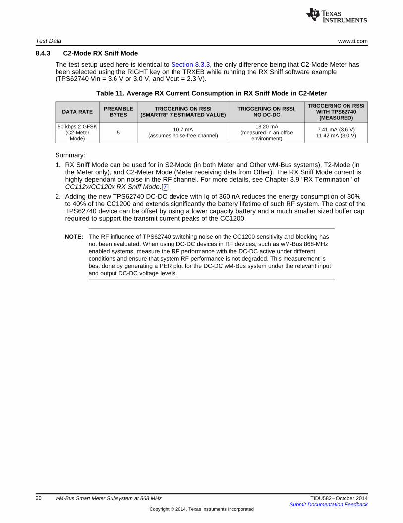
8.4.3 C2-Mode RX Sniff ModeThe test setup used here is identical to Section 8.3.3, the only difference being that C2-Mode Meter hasbeen selected using the RIGHT key on the TRXEB while running the RX Sniff software example(TPS62740 Vin = 3.6 V or 3.0 V, and Vout = 2.3 V).
Table 11. Average RX Current Consumption in RX Sniff Mode in C2-Meter
TRIGGERING ON RSSIPREAMBLE TRIGGERING ON RSSI TRIGGERING ON RSSI,DATA RATE WITH TPS62740BYTES (SMARTRF 7 ESTIMATED VALUE) NO DC-DC (MEASURED)50 kbps 2-GFSK 13.20 mA10.7 mA 7.41 mA (3.6 V)(C2-Meter 5 (measured in an office(assumes noise-free channel) 11.42 mA (3.0 V)Mode) environment)
Summary:1. RX Sniff Mode can be used for in S2-Mode (in both Meter and Other wM-Bus systems), T2-Mode (in
the Meter only), and C2-Meter Mode (Meter receiving data from Other). The RX Sniff Mode current ishighly dependant on noise in the RF channel. For more details, see Chapter 3.9 "RX Termination" ofCC112x/CC120x RX Sniff Mode.[7]
2. Adding the new TPS62740 DC-DC device with Iq of 360 nA reduces the energy consumption of 30%to 40% of the CC1200 and extends significantly the battery lifetime of such RF system. The cost of theTPS62740 device can be offset by using a lower capacity battery and a much smaller sized buffer caprequired to support the transmit current peaks of the CC1200.
NOTE: The RF influence of TPS62740 switching noise on the CC1200 sensitivity and blocking hasnot been evaluated. When using DC-DC devices in RF devices, such as wM-Bus 868-MHzenabled systems, measure the RF performance with the DC-DC active under differentconditions and ensure that system RF performance is not degraded. This measurement isbest done by generating a PER plot for the DC-DC wM-Bus system under the relevant inputand output DC-DC voltage levels.
20 wM-Bus Smart Meter Subsystem at 868 MHz TIDU582–October 2014Submit Documentation Feedback
Copyright © 2014, Texas Instruments Incorporated
L1 is a Bead to be mounted if the regulator U2and capacitors C12 and C41 are not mounted. Bydefault the regulator is not mounted
CC120x using XTAL: do not mount X2, C321, C322 R321, R322CC120x using TCXO: do not mount R12, R321, C311, X1, C301: mount 0 Ohm resistor
R12 is a 0 Ohms shunt resistor that groundthe EXT_OSC pin when TCXO is not mounted
Default mount 2-3
40MHz
DCPL_XOSC
DCPL_XOSC
GPIO0GPIO2CSNSCLKMOSIMISO
RESETGPIO3
RESET
GPIO3
GPIO0
CSN
SCLKMOSI
GPIO2MISO
GPIO0GPIO2CSNSCLKMOSIMISO
VDD_REG
GND
3V3AVDD_REG
VDD_REG
VDD_REG
VDD_REG
3V3A
C31115pF
R141
56k
C1761pF
FIDU3
P3SMA-10V21-TGG
1
2
3 4
5
CC120xRHB
U3
RESET_N2
SI7
SCLK8
CS_N11
RBIAS14
LNA_P19
LNA_N20
XOSC_Q130
XOSC_X231
EXT_OSC32
EGP33
VDD_GUARD1
GPIO33GPIO24
DVDD5
DCPL6
SO(GPIO1)9GPIO010
DVDD12
AVDD_IF13
AVDD_RF15
NC16
PA17
TRX_SW18
DCPL_VCO21
AVDD_SYNTH122
AVDD_PFD_CHP25
DCPL_PFD_CHP26
AVDD_SYNTH227
AVDD_XOSC28
DCPL_XOSC29
LPF023
LPF124
L17318nH
C2013.3pF
L19312nH
TG-5021CG
X2
NC1
GND2
OUT3
VCC4
C30115pF
C17110nF
FIDU5
X140MHz
1
2 4
3
Ant21pF
C17333pFR171
10
P4
CONN_8
12345678
C17415pF
C52
2.2uF
C61
220nF
C251
47nF
C221
47nFC322DNM
C41
DNM_0402
R12
0
L20112nH
C1913.3pF
FIDU2
C12
DNM_0402
C1753pF
L17412nH
R181
0
12
3
C302DNM_0402
L19212nH
TPS79330
U2
IN1
GND2
EN3
NR4
OUT5
C231
1.5nF
C291
47nF
FIDU4
C1812.2pF
C172100pF
C177DNM_0402
L19115nH
C151
47nF
C281
47nF
C131
47nF
C271
47nF
FIDU6
C121
47nF
C261
47nF
R321DNM
A1
ANTENNA
1
L17110nH
P1
SFM-110-02-S-D-A-K-TR
13579
1113151719
2468101214161820
L1727.5nH
C51
47nF
R322
DNM
P2
SFM-110-02-S-D-A-K-TR
13579
1113151719
2468101214161820
FIDU1
L1
BLM15HG102SN1
C211
10nF
C321DNM
Ant1DNM_0402
Ant312nH
C11
47nF
www.ti.com Design Files
9 Design Files
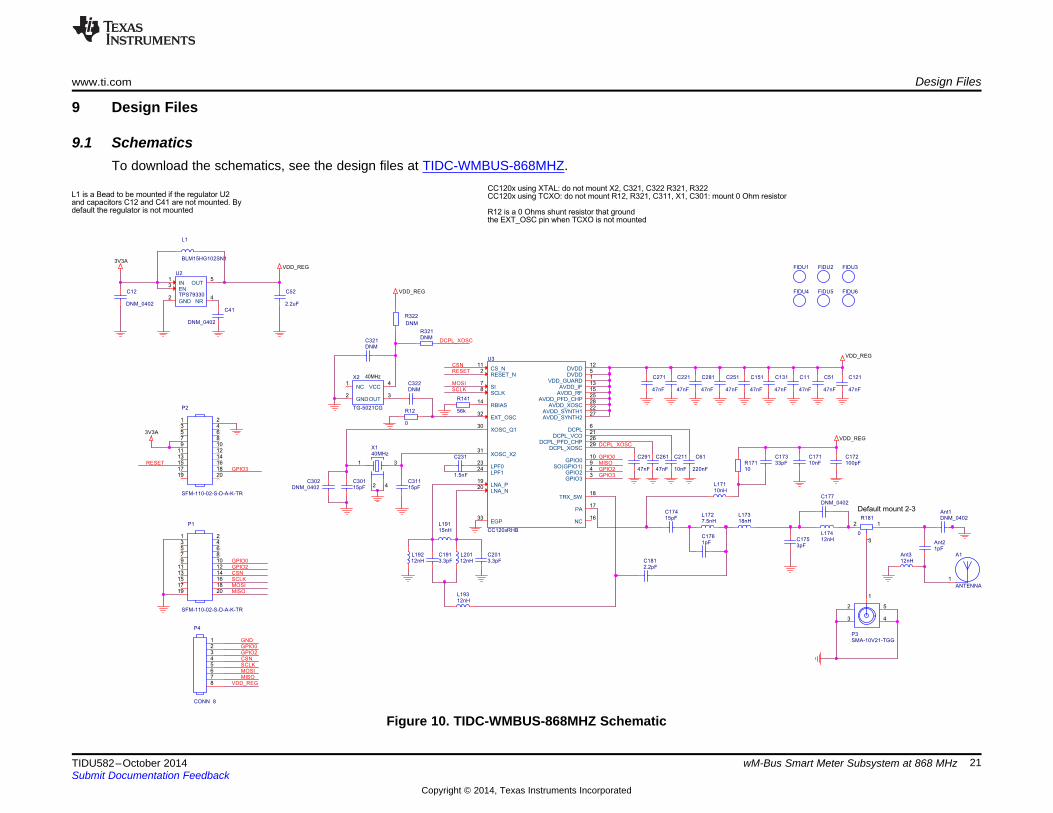
9.1 SchematicsTo download the schematics, see the design files at TIDC-WMBUS-868MHZ.
Figure 10. TIDC-WMBUS-868MHZ Schematic
21TIDU582–October 2014 wM-Bus Smart Meter Subsystem at 868 MHzSubmit Documentation Feedback
Copyright © 2014, Texas Instruments Incorporated

Design Files www.ti.com
22 wM-Bus Smart Meter Subsystem at 868 MHz TIDU582–October 2014Submit Documentation Feedback
Copyright © 2014, Texas Instruments Incorporated
www.ti.com Design Files
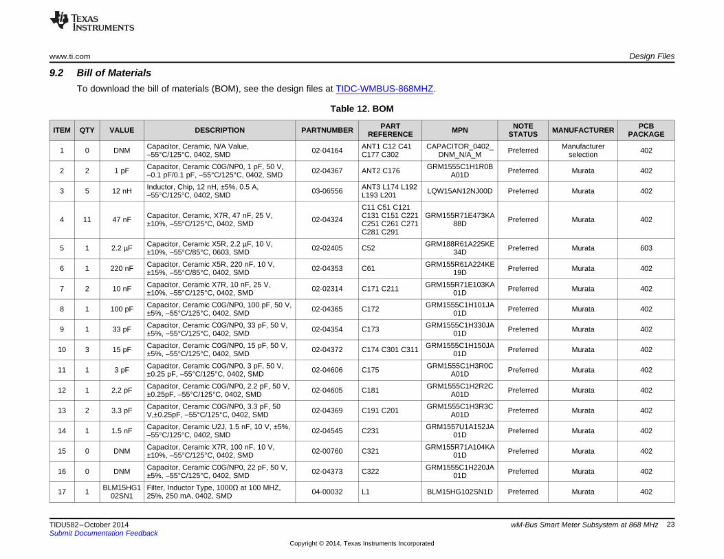
9.2 Bill of MaterialsTo download the bill of materials (BOM), see the design files at TIDC-WMBUS-868MHZ.
Table 12. BOM
PART NOTE PCBITEM QTY VALUE DESCRIPTION PARTNUMBER MPN MANUFACTURERREFERENCE STATUS PACKAGECapacitor, Ceramic, N/A Value, ANT1 C12 C41 CAPACITOR_0402_ Manufacturer1 0 DNM 02-04164 Preferred 402–55°C/125°C, 0402, SMD C177 C302 DNM_N/A_M selectionCapacitor, Ceramic C0G/NP0, 1 pF, 50 V, GRM1555C1H1R0B2 2 1 pF 02-04367 ANT2 C176 Preferred Murata 402–0.1 pF/0.1 pF, –55°C/125°C, 0402, SMD A01DInductor, Chip, 12 nH, ±5%, 0.5 A, ANT3 L174 L1923 5 12 nH 03-06556 LQW15AN12NJ00D Preferred Murata 402–55°C/125°C, 0402, SMD L193 L201
C11 C51 C121Capacitor, Ceramic, X7R, 47 nF, 25 V, C131 C151 C221 GRM155R71E473KA4 11 47 nF 02-04324 Preferred Murata 402±10%, –55°C/125°C, 0402, SMD C251 C261 C271 88D
C281 C291Capacitor, Ceramic X5R, 2.2 µF, 10 V, GRM188R61A225KE5 1 2.2 µF 02-02405 C52 Preferred Murata 603±10%, –55°C/85°C, 0603, SMD 34DCapacitor, Ceramic X5R, 220 nF, 10 V, GRM155R61A224KE6 1 220 nF 02-04353 C61 Preferred Murata 402±15%, –55°C/85°C, 0402, SMD 19DCapacitor, Ceramic X7R, 10 nF, 25 V, GRM155R71E103KA7 2 10 nF 02-02314 C171 C211 Preferred Murata 402±10%, –55°C/125°C, 0402, SMD 01DCapacitor, Ceramic C0G/NP0, 100 pF, 50 V, GRM1555C1H101JA8 1 100 pF 02-04365 C172 Preferred Murata 402±5%, –55°C/125°C, 0402, SMD 01DCapacitor, Ceramic C0G/NP0, 33 pF, 50 V, GRM1555C1H330JA9 1 33 pF 02-04354 C173 Preferred Murata 402±5%, –55°C/125°C, 0402, SMD 01DCapacitor, Ceramic C0G/NP0, 15 pF, 50 V, GRM1555C1H150JA10 3 15 pF 02-04372 C174 C301 C311 Preferred Murata 402±5%, –55°C/125°C, 0402, SMD 01DCapacitor, Ceramic C0G/NP0, 3 pF, 50 V, GRM1555C1H3R0C11 1 3 pF 02-04606 C175 Preferred Murata 402±0.25 pF, –55°C/125°C, 0402, SMD A01DCapacitor, Ceramic C0G/NP0, 2.2 pF, 50 V, GRM1555C1H2R2C12 1 2.2 pF 02-04605 C181 Preferred Murata 402±0.25pF, –55°C/125°C, 0402, SMD A01DCapacitor, Ceramic C0G/NP0, 3.3 pF, 50 GRM1555C1H3R3C13 2 3.3 pF 02-04369 C191 C201 Preferred Murata 402V,±0.25pF, –55°C/125°C, 0402, SMD A01DCapacitor, Ceramic U2J, 1.5 nF, 10 V, ±5%, GRM1557U1A152JA14 1 1.5 nF 02-04545 C231 Preferred Murata 402–55°C/125°C, 0402, SMD 01DCapacitor, Ceramic X7R, 100 nF, 10 V, GRM155R71A104KA15 0 DNM 02-00760 C321 Preferred Murata 402±10%, –55°C/125°C, 0402, SMD 01DCapacitor, Ceramic C0G/NP0, 22 pF, 50 V, GRM1555C1H220JA16 0 DNM 02-04373 C322 Preferred Murata 402±5%, –55°C/125°C, 0402, SMD 01D
BLM15HG1 Filter, Inductor Type, 1000Ω at 100 MHZ,17 1 04-00032 L1 BLM15HG102SN1D Preferred Murata 40202SN1 25%, 250 mA, 0402, SMD
23TIDU582–October 2014 wM-Bus Smart Meter Subsystem at 868 MHzSubmit Documentation Feedback
Copyright © 2014, Texas Instruments Incorporated
Design Files www.ti.com
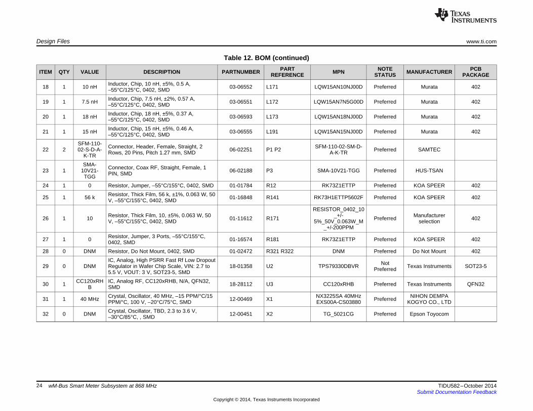
Table 12. BOM (continued)PART NOTE PCBITEM QTY VALUE DESCRIPTION PARTNUMBER MPN MANUFACTURERREFERENCE STATUS PACKAGE
Inductor, Chip, 10 nH, ±5%, 0.5 A,18 1 10 nH 03-06552 L171 LQW15AN10NJ00D Preferred Murata 402–55°C/125°C, 0402, SMDInductor, Chip, 7.5 nH, ±2%, 0.57 A,19 1 7.5 nH 03-06551 L172 LQW15AN7N5G00D Preferred Murata 402–55°C/125°C, 0402, SMDInductor, Chip, 18 nH, ±5%, 0.37 A,20 1 18 nH 03-06593 L173 LQW15AN18NJ00D Preferred Murata 402–55°C/125°C, 0402, SMDInductor, Chip, 15 nH, ±5%, 0.46 A,21 1 15 nH 03-06555 L191 LQW15AN15NJ00D Preferred Murata 402–55°C/125°C, 0402, SMD
SFM-110- Connector, Header, Female, Straight, 2 SFM-110-02-SM-D-22 2 02-S-D-A- 06-02251 P1 P2 Preferred SAMTECRows, 20 Pins, Pitch 1.27 mm, SMD A-K-TRK-TRSMA- Connector, Coax RF, Straight, Female, 123 1 10V21- 06-02188 P3 SMA-10V21-TGG Preferred HUS-TSANPIN, SMDTGG
24 1 0 Resistor, Jumper, –55°C/155°C, 0402, SMD 01-01784 R12 RK73Z1ETTP Preferred KOA SPEER 402Resistor, Thick Film, 56 k, ±1%, 0.063 W, 5025 1 56 k 01-16848 R141 RK73H1ETTP5602F Preferred KOA SPEER 402V, –55°C/155°C, 0402, SMD
RESISTOR_0402_10Resistor, Thick Film, 10, ±5%, 0.063 W, 50 _+/- Manufacturer26 1 10 01-11612 R171 Preferred 402V, –55°C/155°C, 0402, SMD 5%_50V_0.063W_M selection
_+/-200PPMResistor, Jumper, 3 Ports, –55°C/155°C,27 1 0 01-16574 R181 RK73Z1ETTP Preferred KOA SPEER 4020402, SMD
28 0 DNM Resistor, Do Not Mount, 0402, SMD 01-02472 R321 R322 DNM Preferred Do Not Mount 402IC, Analog, High PSRR Fast Rf Low Dropout Not29 0 DNM Regulator in Wafer Chip Scale, VIN: 2.7 to 18-01358 U2 TPS79330DBVR Texas Instruments SOT23-5Preferred5.5 V, VOUT: 3 V, SOT23-5, SMD
CC120xRH IC, Analog RF, CC120xRHB, N/A, QFN32,30 1 18-28112 U3 CC120xRHB Preferred Texas Instruments QFN32B SMDCrystal, Oscillator, 40 MHz, –15 PPM/°C/15 NX3225SA 40MHz NIHON DEMPA31 1 40 MHz 12-00469 X1 PreferredPPM/°C, 100 V, –20°C/75°C, SMD EXS00A-CS03880 KOGYO CO., LTDCrystal, Oscillator, TBD, 2.3 to 3.6 V,32 0 DNM 12-00451 X2 TG_5021CG Preferred Epson Toyocom–30°C/85°C, , SMD
24 wM-Bus Smart Meter Subsystem at 868 MHz TIDU582–October 2014Submit Documentation Feedback
Copyright © 2014, Texas Instruments Incorporated
www.ti.com Design Files
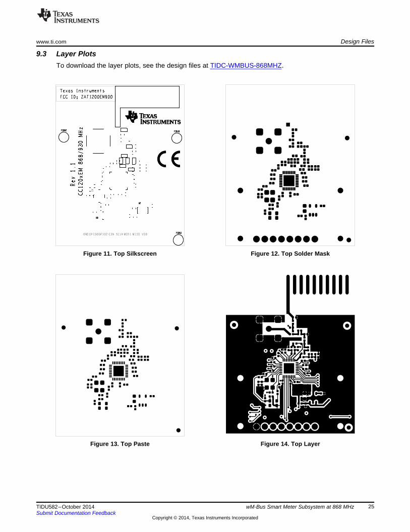
9.3 Layer PlotsTo download the layer plots, see the design files at TIDC-WMBUS-868MHZ.
Figure 11. Top Silkscreen Figure 12. Top Solder Mask
Figure 13. Top Paste Figure 14. Top Layer
25TIDU582–October 2014 wM-Bus Smart Meter Subsystem at 868 MHzSubmit Documentation Feedback
Copyright © 2014, Texas Instruments Incorporated
Design Files www.ti.com
Figure 15. Ground Plane Layer 2 Figure 16. PWR Plane Layer 3
Figure 17. Bottom Layer Figure 18. Bottom Paste
26 wM-Bus Smart Meter Subsystem at 868 MHz TIDU582–October 2014Submit Documentation Feedback
Copyright © 2014, Texas Instruments Incorporated
www.ti.com Design Files
Figure 19. Bottom Solder Mask Figure 20. Bottom Silkscreen
Figure 21. Drill Drawing Figure 22. Board Outline
9.4 CAD ProjectTo download the CAD project files, see the design files at TIDC-WMBUS-868MHZ.
9.5 Gerber FilesTo download the Gerber files, see the design files at TIDC-WMBUS-868MHZ.
27TIDU582–October 2014 wM-Bus Smart Meter Subsystem at 868 MHzSubmit Documentation Feedback
Copyright © 2014, Texas Instruments Incorporated
Design Files www.ti.com
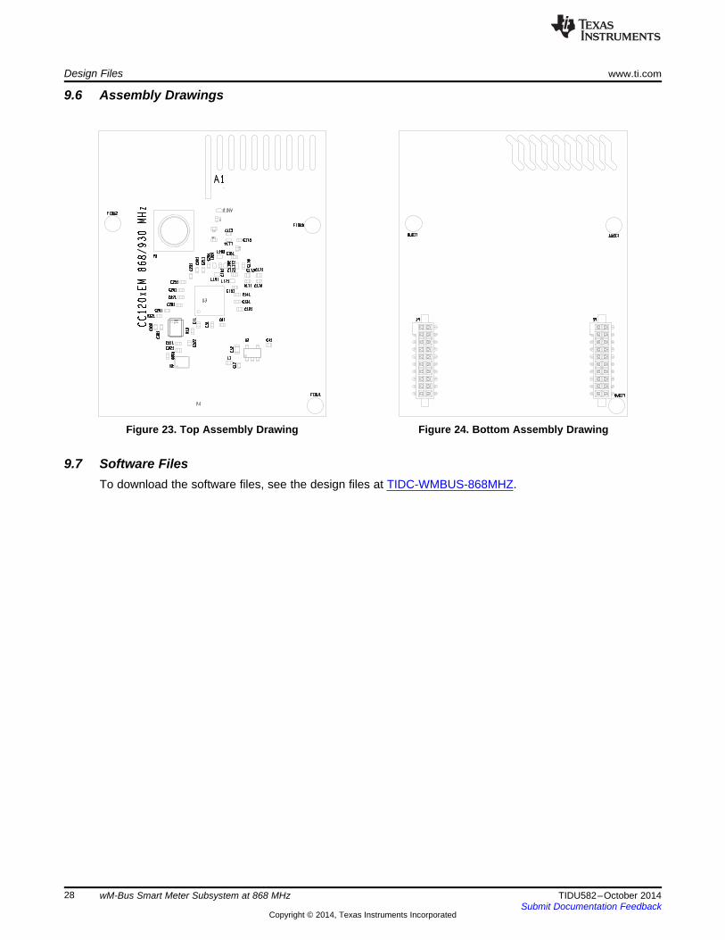
9.6 Assembly Drawings
Figure 23. Top Assembly Drawing Figure 24. Bottom Assembly Drawing
9.7 Software FilesTo download the software files, see the design files at TIDC-WMBUS-868MHZ.
28 wM-Bus Smart Meter Subsystem at 868 MHz TIDU582–October 2014Submit Documentation Feedback
Copyright © 2014, Texas Instruments Incorporated
www.ti.com References
10 References
1. Texas Instruments, CC1200 Datasheet (SWRS123D)2. Texas Instruments, TPS62740 Datasheet (SLVSAC3C)3. Beuth, EN13757-4:2014-02 (wM-Bus Standard Document)4. Texas Instruments, Application Note AN121, Wireless M-Bus Implementation with CC112x / CC120x
High Performance Transceiver Family (SWRA423)5. Texas Instruments, Design Note DN039, Matched Integrated Passive Component for 868 / 915 MHz
operation with the CC112x, CC117x & CC12xx high performance radio series (SWRA407)6. Texas Instruments, Design Note DN040, Reduced Battery Current Using CC112x/CC1175/CC1200
with TPS62730 (SWRA411)7. Texas Instruments, Application Report, CC112x/CC120x RX Sniff Mode (SWRA428A)8. ETSI 300220 v2.4.1 (Web)9. Texas Instruments, Application Note AN098, Layout Review Techniques for Low Power RF Designs
(SWRA367)10. Texas Instruments, Application Note AN068, Adapting TI LPRF Reference Designs for Layer Stacking
(SWRA236A)11. Texas Instruments, SmartRF Studio 7 (Link)
11 TerminologywM-Bus— The European RF Metering standard, providing solutions for 169-, 433-, and 868-MHz bands
ETSI Cat. 2 Receiver—The definition for a set of RF parameters in EN300 220 v2.4.1, representing theminimum requirement in wM-Bus capable RF systems at 868 MHz
S-Mode— wM-Bus Mode at 868 MHz at 32.768 kcps (net of 16.384 kbps), mandated in Germany
T-Mode— wM-Bus Mode at 868 MHz at 100 kcps (net of 66.667 kbps), mandated in Germany andNetherlands
C-Mode— The “new” or improved "T-Mode" at 868 MHz at 100 kcps (net of 100 kbps), mandated inGermany
12 About the AuthorMILEN STEFANOV is a system applications engineer at Texas Instruments, where he is responsible forSub-1 GHz RF communications solutions for Smart Meters. Milen has significantly contributed todelivering TI’s full wM-Bus system solution, consisting of an MCU+RF chipset, a complete wM-Busprotocol stack, and a dedicated power management solution. Milen has a system-level expertise on smartmetering and RF communications and over 15 years of experience working with customers. He haspublished several technical articles on wM-Bus related topics in the past four years. He earned his masterof science in electrical engineering (MSEE) from Technical University in Chemnitz, Germany.
29TIDU582–October 2014 wM-Bus Smart Meter Subsystem at 868 MHzSubmit Documentation Feedback
Copyright © 2014, Texas Instruments Incorporated
IMPORTANT NOTICE FOR TI REFERENCE DESIGNS
Texas Instruments Incorporated ("TI") reference designs are solely intended to assist designers (“Buyers”) who are developing systems thatincorporate TI semiconductor products (also referred to herein as “components”). Buyer understands and agrees that Buyer remainsresponsible for using its independent analysis, evaluation and judgment in designing Buyer’s systems and products.TI reference designs have been created using standard laboratory conditions and engineering practices. TI has not conducted anytesting other than that specifically described in the published documentation for a particular reference design. TI may makecorrections, enhancements, improvements and other changes to its reference designs.Buyers are authorized to use TI reference designs with the TI component(s) identified in each particular reference design and to modify thereference design in the development of their end products. HOWEVER, NO OTHER LICENSE, EXPRESS OR IMPLIED, BY ESTOPPELOR OTHERWISE TO ANY OTHER TI INTELLECTUAL PROPERTY RIGHT, AND NO LICENSE TO ANY THIRD PARTY TECHNOLOGYOR INTELLECTUAL PROPERTY RIGHT, IS GRANTED HEREIN, including but not limited to any patent right, copyright, mask work right,or other intellectual property right relating to any combination, machine, or process in which TI components or services are used.Information published by TI regarding third-party products or services does not constitute a license to use such products or services, or awarranty or endorsement thereof. Use of such information may require a license from a third party under the patents or other intellectualproperty of the third party, or a license from TI under the patents or other intellectual property of TI.TI REFERENCE DESIGNS ARE PROVIDED "AS IS". TI MAKES NO WARRANTIES OR REPRESENTATIONS WITH REGARD TO THEREFERENCE DESIGNS OR USE OF THE REFERENCE DESIGNS, EXPRESS, IMPLIED OR STATUTORY, INCLUDING ACCURACY ORCOMPLETENESS. TI DISCLAIMS ANY WARRANTY OF TITLE AND ANY IMPLIED WARRANTIES OF MERCHANTABILITY, FITNESSFOR A PARTICULAR PURPOSE, QUIET ENJOYMENT, QUIET POSSESSION, AND NON-INFRINGEMENT OF ANY THIRD PARTYINTELLECTUAL PROPERTY RIGHTS WITH REGARD TO TI REFERENCE DESIGNS OR USE THEREOF. TI SHALL NOT BE LIABLEFOR AND SHALL NOT DEFEND OR INDEMNIFY BUYERS AGAINST ANY THIRD PARTY INFRINGEMENT CLAIM THAT RELATES TOOR IS BASED ON A COMBINATION OF COMPONENTS PROVIDED IN A TI REFERENCE DESIGN. IN NO EVENT SHALL TI BELIABLE FOR ANY ACTUAL, SPECIAL, INCIDENTAL, CONSEQUENTIAL OR INDIRECT DAMAGES, HOWEVER CAUSED, ON ANYTHEORY OF LIABILITY AND WHETHER OR NOT TI HAS BEEN ADVISED OF THE POSSIBILITY OF SUCH DAMAGES, ARISING INANY WAY OUT OF TI REFERENCE DESIGNS OR BUYER’S USE OF TI REFERENCE DESIGNS.TI reserves the right to make corrections, enhancements, improvements and other changes to its semiconductor products and services perJESD46, latest issue, and to discontinue any product or service per JESD48, latest issue. Buyers should obtain the latest relevantinformation before placing orders and should verify that such information is current and complete. All semiconductor products are soldsubject to TI’s terms and conditions of sale supplied at the time of order acknowledgment.TI warrants performance of its components to the specifications applicable at the time of sale, in accordance with the warranty in TI’s termsand conditions of sale of semiconductor products. Testing and other quality control techniques for TI components are used to the extent TIdeems necessary to support this warranty. Except where mandated by applicable law, testing of all parameters of each component is notnecessarily performed.TI assumes no liability for applications assistance or the design of Buyers’ products. Buyers are responsible for their products andapplications using TI components. To minimize the risks associated with Buyers’ products and applications, Buyers should provideadequate design and operating safeguards.Reproduction of significant portions of TI information in TI data books, data sheets or reference designs is permissible only if reproduction iswithout alteration and is accompanied by all associated warranties, conditions, limitations, and notices. TI is not responsible or liable forsuch altered documentation. Information of third parties may be subject to additional restrictions.Buyer acknowledges and agrees that it is solely responsible for compliance with all legal, regulatory and safety-related requirementsconcerning its products, and any use of TI components in its applications, notwithstanding any applications-related information or supportthat may be provided by TI. Buyer represents and agrees that it has all the necessary expertise to create and implement safeguards thatanticipate dangerous failures, monitor failures and their consequences, lessen the likelihood of dangerous failures and take appropriateremedial actions. Buyer will fully indemnify TI and its representatives against any damages arising out of the use of any TI components inBuyer’s safety-critical applications.In some cases, TI components may be promoted specifically to facilitate safety-related applications. With such components, TI’s goal is tohelp enable customers to design and create their own end-product solutions that meet applicable functional safety standards andrequirements. Nonetheless, such components are subject to these terms.No TI components are authorized for use in FDA Class III (or similar life-critical medical equipment) unless authorized officers of the partieshave executed an agreement specifically governing such use.Only those TI components that TI has specifically designated as military grade or “enhanced plastic” are designed and intended for use inmilitary/aerospace applications or environments. Buyer acknowledges and agrees that any military or aerospace use of TI components thathave not been so designated is solely at Buyer's risk, and Buyer is solely responsible for compliance with all legal and regulatoryrequirements in connection with such use.TI has specifically designated certain components as meeting ISO/TS16949 requirements, mainly for automotive use. In any case of use ofnon-designated products, TI will not be responsible for any failure to meet ISO/TS16949.IMPORTANT NOTICE
Mailing Address: Texas Instruments, Post Office Box 655303, Dallas, Texas 75265Copyright © 2015, Texas Instruments Incorporated