Embed Size (px)
Citation preview

01Wt ©WoM RL-TR-94-18500- Final Technical ReportN Ocober 1994
DESIGN, FABRICATION, ANDCHARACTERIZATION OF REFLECTIVEDIFFRACTIVE OPTICAL ELEMENTS IN SiFOR FREE-SPACE OPTICALINTERCONNECTS
Cornell University $i,) 1" '.ftE LECTVgl•Steven M. Shank and Harold G. Craighead GT 2 2.1
APPROVED FOR PUBLW RELEASE," DISTRIUTIN UNLIMITED.
94 11 22 058
94-35898 DTIC 8UALITY T'jT
Rome LaboratoryAir Force Materel Command
Griffiss Air Force Base, New York

I #
This report has been reviewed by the Rome Laboratory Public Affairs Office(PA) and is releasable to the National Technical Information Service (NTIS). AtNTIS it will be releasable to the general public, including ;oreign natirns.
RL-TR-94-185 has been reviewed and is approved for publication.
APPROVED:
FMANZ HAASProject Engineer
FOR THE COMM4ANDER;~ /QIDONALD W. HANISONDirector of Surveillance & Photonics
If your address has changed or if you wish to be removed from the Rome Laboratorymailing list, or if th, addressee is no longer @mploved by your organization,please notify RL ( O('PB) Griffiss AFB NY 13441. This will assist us in maintaininga current mailing list.
Do not return copies of this report unless contractual obligations or notices on Aspecific document requiri that it be returned.

REPORT DOCUMENTATION PAGE F0MB8 NAO%7O40-1 8 8
-- I 40INO #'.*9S W W, , Sb~w s uw ObalsmIf- OW O1""YANU WWA MSt' 2'
St111111011 and Ishank-W and Harol PC.w P"~gea mwV -N044 rr 1 N c
1. AGENY USE NLY IL hWO REORT DAT I R PkRT 1 NDUDAE$ OE
Octtobel 19anoFibrl Feb 93Facility
4. TE AD KSIME&GENDY NUMBERSMBE
6t ALTHWNTW TAO-EP
Steve Maboratok an Hro ldc nGin. r Fraihand HasiC 5 33 -2131
72a EPOOAM RBJTIOUATWH P&MY STATND DI&S &a.F~*N OWIRGllNIZATON
Napproned fSar ublic rlae dsrbtion uFlimited
iaeconc wheeb aS ax arrayOP AGfC LE)s NO focuuedS ont a 4x4 aray fW4A~~
Rhotodetecrtor.. (OPro s develpCen for' hihyefcetUifatv l Men ERi
d25rind iE-ee ifatv lmnsaefbiae sn lectroni bean
koelectron iraoacy arjc ndgtoier Forcez miros/cpy, 15 330dvceprfrane1sdeemie
byroe mes rig dubifrcto rlaeffdic tienc i onus.itd
na ASW.ICTIONw"52oDiffractive elpetic , eleetrosin s b am e lihoraphye freactiv -pae ionedotia
ineronec weeb a4x Sara f LEDs IsLSSFE foue nt xLaryophoodeectra Prcca deelpmet fr hghy eficentdifrativ elmets~~m2S is
pre~pte. Farictio tolranes fr bnar levl aignmnt nd tch ept2ar

Acoession ForNTIS GrA&I
DTIC TAB
UrRInno i cod -
By .. . . .DL• Y1.1t,•, L". ý.,ý,jL..
Avcalt h I :' """ c~o
Table of Contents i
T ab le o f C o n ten ts ...................................................................................................................... iiiL ist o f Fig u res ............................................................................................................ . . . . . iv1 . In tro d u ctio n ............................................................................................................................ 12. Design of an off-axis, reflecti ve, imaging diffractive optical element ................. 4
2.1. DOE design using equal path length modulo A arguments .............................. 42.2. DOE design using the interference of two spherical waves generated by two
p o in t so u rces .......................................................................................................... . . 92.3. DOE surface relief and effects on efficiency ........................................................ 112.4. Effects on surface relief due to off-axis operation .............................................. 13
3. Process development, fabrication, and characterization of DOEs using electronbeam lithography and reactive ion etching, and focused ion beam milling ............ 15
3.1. Process development and characterization of fabrication of DOEs usingelectron beam lithography and reactive ion etching ........................................ 15
3.1.1. Process overview .......................................................................................... 153.1.2. A lignm ent m arks .......................................................................................... 173.1.3. Thin film SiO evaporation ........................................................................... 213.1.4. DOE pattern definition and electron beam lithography .......................... 223.1.5. Proximity effects on grating fabrication ..................................................... 243.1.6. Reactive ion etching ..................................................................................... 283.1.7. Characterization of grating etch depths using atomic force microscopy .... 31
3.2. Process developmer. and characterization of DOEs fabricated by focused
ion beam m illing .................................................................................................. . . 344. D evice perform ance ......................................................................................................... 375. Conclusions and ongoing work ..................................................................................... 396 . R eferen ces ............................. ............................................................................................... 40

List of Figures
Figure 2.1a Schematic representation of a DOE and parameters used to calculate phasecon tou rs .................................................................................................................... 5
Figure 2.1b. Unfolded view of the diagram used to setup calculation of the phase zoneendpoints of the focusing, reflective DOE ............................. 5
Figure 2.2. Phase contours generated using FREDD and equations (2.4)-(2.7) ....... 8Figure 2.3. Efficiency versus diffraction order for (a) 2-, (b) 4-, and (c) 8-level binary
surface relief profiles ........................................................................................ 12Figure 2.4. Surface relief for off-axis rays ......................................................................... 14
Figure 3.1. Overview of fabrication process for diffractive optical element in Si ........ 16Figure 3.2. CAD pattern of a global alignment mark used to correct for rotation and
translation errors at the wafer level ............................................................... 18Figure 3.3. Process for fabricating alignment marks ....................................................... 19Figure 3.4. BPD data of a fractured subzone .................................................................... 23Figure 3.5. Schematic representation of the effects of (a) overexposure and (b)
underexposure on the alignment of binary levels ........................ 25
Figure 3.6. % pixel error versus dose for DOE feature sizes ........................................... 26Figure 3.7. Linear gratings fabricated at electron beam doses of (a) 50gC/cm2, (b)
60pC/cm2, ,c) 70pC/cm2, and (d) 80C/cm2 . . . . . . . . . . . . . . . . . . ... ..... 27Figure 3.8. One (left) and several (right) periods of an 8-level linear grating ............. 29Figure 3.9. Si etch depth versus etch time for different flow rates, cheinber pressures,
and sam ple biases ............................................................................................. 30Figure 3.10. Diffraction efficiency versus etch error for 4- and 8-level binary surface
reliefs ....................................................................................................................... 32Figure 3.11. AFM surface profile (top) and line scan (bottom) of several periods of an
8-level linear grating fabricated at 60p.C/cm2 ......................... ........... ..... . . . 33Figure 3.12. AFM surface profile (top) and line scan (bottom) of several periods of a
continuously blazed grating fabricated using focused ion beam milling....35Figure 4.1. Rendered CCD image of diffraction pattern of the 8-level linear grating
described in text ................................................................................................ 38
LM

1. Introduction
The ability to fabricate integrated circuits with many densely packed devices that
switch at high speeds, has produced the situation that the limitations in computing
speeds are not due to on-chip processing effects, but are due to chip-to-chip and board-
to-board interconnections. Fundamental limitations of electrical interconnections
include cross-talk, energy radiation, clock skew, capacitive loading, and the difficulty of
crossing wires without interference, all of which detrimentally effect the ability to
transport high bandwidth data at high speeds using sophisticated, massively parallel
and dense interconnect schemes, with highly precise clock signal distribution. These
limitations are particularly severe for microwave signal communications where GHz
clock rates limit electrical interconnects to a length range of mm to cm. 1 Multi-chip
modules (MCMs), which have reduced interconnection length, reduced capacitive
loading of the interconnects, smaller lead inductance, reduced size and weight, and
reduced power consumption, compared to their printed circuit board (PCB)
counterparts, have been developed for microprocessor rates in the 50-200MHz range
where they outperform PCBs by over 100%.2 MCMs also increase the number of
possible interconruects which is essential for the efficient operation of advanced
architecture CPU's such as RISC or CISC. 2 However, as the number of interconnections
increase, the minimum pin spacing where acceptable signal cross coupling occurs will
be reached and as clock rates increase to the GHz regime, an alternative to a purely
electrical MCM technology will be required. 3,4
One such alternative is a hybrid architecture of planar electrical interconnects,
and vertical, free-space optical intercornnects for use in stacked MCMs. 5,6 In previous
final technical reports, the development of a free-space optical interconnect was
described. 7A Complete chip sets were fabricated, including light emitting diode (LED)
, m I
arrays6, diffractive optics9, and photodetector arrays. These clhips were designed and
fabricated to be compatible with current MCM technology. Work is currently in
progress on incorporating the LED and photodetector chips in a MCM package
manufactured by the General Electric Company.
In this report, further developments of the design, fabrication, and testing of the
diffractive optics chip is discussed. This chip consists of a focusing, reflective, off-axis,
diffractive optical element (DOE) that was designed to image a 4x4 array of GaAsP
LEDs onto a 4x4 array of metal-semiconductor-metal silicon photodetectors. 7 Although
the design of transmissive architectures is more commonl 1,12, the use of a reflective
geometry offers several advantages for both the MCM and DOE fabrication.
Advantages for the MCM include patterned chips on a single side, the use of electrically
active chips that face the same direction, and the use of semiconductor device substrates
that are not required to be optically transparent. Advantages in the fabrication of
reflective DOEs include buried diffractive and reflective surfaces 13, shallower etched
features, the ability to use the optic without an anti-reflection coating, and a decoupled
substrate volume from the optic, which allows for the use of standard silicon processing
techniques for the fabrication of the DOE.9 Section 2 of this report presents the design of
the DOE using two different methods. The first method defines the phase contours of
the DOE using equal path length modulo X arguments. The second method uses the
interference of two spherical waves to define the phas( contours. This second method
clearly points out that the DOEs that we are fabricating, are computer generated
holograms. Section 2 also includes a discussion of the DOE design for maximizing the
efficiency of the device by fabricating the surface relief for imaging using the first
diffracted order. In section 3, the fabrication of 8-level DOEs using electron beam
lithography and reactive ien etching (RIE) and the fabrication of continuously graded
gratings using focused ion beam (FIB) milling is described. The characterization of these
2

devices by scanning electron microscopy (SEM) and atomic force microscopy (AFM)
and an analysis of diffraction efficiency based on these characterization results is also
presented. In section 4, preliminary results of the performances of linear test gratings
are presented, and in section 5, conclusions and ongoing work are described.

2. Design of an off-axis, reflective, imaging diffractive optical element
2.1. DOE design using equal path length modulo X arguments
The DOE consists of phase zones that are designed to image light by constructive
interference. Each phase zone has a surface relief designed such that diffraction is
maximized for the first order, thereby producing the potential for a highly efficient
imaging device. The intersection of the plane of the optic with the family of confocal
ellipsoids with foci at the desired object and image points, defines the phase zones of
the DOE. The object and image points of the grating are taken to be the centers of the
LED and photodetector arrays, respectively. The center of each phase zone is the point
on the substrate where specular reflection connects the object and image points. This
distance between object and image points through the specular point of the grating is
defined as the specular distance. A schematic representation of the DOE is shown in
figure 2.1a. The DOE is designed to be asymmetric in the x direction. This allows for off-
axis operation which is necessary for reflective architectures which do not use
beamsplitters. The DOE is symmetric in the y direction, which is sufficient for point to
point imaging, and unoptimized imaging of object arrays 7 A more sophisticated
approach would average the aberrations across all detector elements and would require
a more general design algorithm. Also shown in figure 2.1a are the parameters used to
calculate the phase contours of the DOE. Figure 2.1b is a schematic of how the endpoint
of a phase zone is calculated. The criteria for calculating these phase zones is that the
sum of the distance from the object (0,0,0) to the endpoint (x,y,z) and the endpoint to the
image (x I,y 1,zl) equals the distance through the specular point modulo X. This is simply
the criteria for constructive interference. This relation is given by,
x2+z+2 +(x-x) 2 +(z1 z)2 +m,= x2 +y 2 +z+ V(xi x) 2 +y 2 +(z1 z) 2 (2.1)
4

Zimage (x1,0,z1 )
object (0,0,0)
Figure 2.1a. Schematic representation of a DOE and the parameters used to calculate phase contours,
image (xi1, 0, z 1)
xs, 0, z) specular point of D,
object (0, 0, 0)
Figure 2.1b. Unfolded view of the diiagram used to setup calculation of the phase zone endpointsof the focusing, reflective DOE. As discussed in the text, the endpoints are determined bysolving for x and y using,
-F~+$xixa)+ (z )+ rk= X2 +Y2 +Z +4(XIX) 2 +y2+(ZIZ) 2
5

where x, y, z, xI, and z1 are parameters given in figure 2.1, A. is the wavelength of the
incident wave (center wavelength of the LED emitters), and m represents the particular
phase zone. To define the surface relief, each phase zone is separated into subzones,
where each subzone defines a surface relief step, with the total number of steps in each
zone approximating a perfectly blazed relief which would image 100% of the incident
intensity of a perfect point source into a point image. 2, 4, and 8 subzones are used to
design 2-, 4-, and 8-level DOEs. These subzones are taken into account by replacing the
mX. term in equation (2.1) with mX./n, where n is the number of binary levels of the
DOE. Equation (2.1) can be solved for x to determine the endpoints of the phase zones.
These endpoints are given by,
XL = (d2 - x'- z'+2zz,)x,2(x' -d')
I~•-• z 1+ 2z,)' -4(X,-d'Id -f -4 ÷•)z~d]S2(x' - d 2) (2.2)
where xe are the endpoints, and d is the specular distance modulo X/n. Once the
endpoints are determined, the phase contours are generated by solving equation (2.1)
for y,
J(d• 2 X2-z 2 + 2z,, + 2xx)S x2_ z2 (2.3)
where the x values in (2.3) are chosen to be evenly spaced between the endpoints Xe.
Equation (2.3) can be further manipulated to be put in the form,Xa h2 +1 = 1 (2.4)
a-2 b 2
6

where,
-X1~ (d I 2 + 2zzl)-x1 (d2 - xl - zl (2.5)
2(x'-d ) (25)
[x(d2 -2 _ •+2zz2 2 -x -z +2zz2) 2 +d2 z 2
a 4(x-d 2) (2.6)(x• -.d').. .(
x(d2 -X2 -•-z• + 2zz,) 2 (d' X2- z_2 + 2z 2)'-
b2 4(x'-d d2 (2.7).
Since equation (2.4) is simply the equation of an ellipse, the phase contours of the DOE
are ellipses centered about (h, 0) with axis lengths of 2a and 2b. The program FREDD
(FREsnel Device Design), which has been previously described 7, uses the algorithms in
equations (2.2) and (2.3) to generate the phase contours of the desired DOE. Figure 2.2
compares several phase contours generated using FREDD with ellipses generated using
equation (2.4). It is clear that from figure 2.2 that the ellipses generated using equation
(2.4) are in agreement with the algorithms of FREDD.

60 r- I 1 I 1 T I I IFREDD calculation
* ellipse O........ ......... .....
40 o ellipse
0 o .( 'S
•' "S
-20 ,, / /
"-40 'C"
-60'
S•I II I ,. ,i I I I ,
540 560 580 600 620 640 660
x(gtm)
Figure 2.2. Phase contours generated using FREDD and equations (2.4) - (2.7).Parameters used to generate the contours are x 1=0.9mm, z=6mm, z -=3mm,X-0=.6328;im, m=1, and n=2.
L [ r l 8

2.2. DOE desigln using the interference of two spherical waves generated by two
point sources
An alternat've to the method for generating phase contours described in section
2.1 is to determine the transmission function t(x,y,z) that will convert a diverging
spherical input wave, Em (x,y,z), that emanates from a point source at (0,0,0) into a
converging spherical wave, Eout(x,y,z), that is imaged to the point (xl, 0, zj). This
relationship is given by,
Eou, (X, y,z)= t(x, y)E1 n (X, y,z) (2.8)
where,
E,,(X,y,z) = Ae''" (2.9)Rin
Eout (xI ,yz) =-L#-,- '° (2.10)Rout
and,
+2-(z-XF 1 )-+2 (x 2+ (2.12)
k = TPX _ ~X1)2 + y2 +-ZZ~l(.2
where the convention has been chosen such that for a diverging spherical wave, the
phase gets more negative farther from the specular point at the DOE plane and for a
converging spherical wave, the phase gets more positive. The situation described in9

equation (2.8) is analogous to the generation of a hologram where the reference beam is
generatd from the object point source and the picture beam is generated from the
image point source. By interfering the reference and picuture beams together at the
(x,y,z) plane, t(x,y,z) is generated. Upon subsequent illumination by Ein, Eout is
generated and the point image at (x 1, 0, zI) is formed. Since for this work the case of
purely phase objects are of interest, t(x,y,z) is given by,
t(x, y,z) =exp[io1] (2.13)
where
0 = -ou, - in (2.14).
The phase function of the DOE, Of is equal to 01 modulo 27c so that the phase is always
constrained between 0 and 2ir, and across phase zone interfaces, the phase is reset from
21c to 0. The phase function of the DOE is therefore given by,
O,(x,y,z)= 4 /[(x-x1 2, +y +(Z-z 1 )2 V'(X - X) 2 +(z-z,) 2 +
x+ + +z2 _Z2 X+2 -mX] (2.15).
The phase zone boundaries are determined by setting of =0, which produces an
expression identical to equation (2.1). The DOE can therefore be thought of a fringe
pattern or hologram that is generated by interfering two point sources. Since the fringe
patterns, or phase contours are written using lithography, instead of being generated by
the optical interference between two point sources, the DOEs can be classified as
computer generated holograms. This formalism is useful for emitters with wave
distributions other than spherical, such as vertical cavity surface emitting lasers, where
10

the wave distributions are Gaussian, and equations (2.9) and (2.10) can be modified
accordingly.
2.3. DOE surface relief and effects on efficiency
The location of the phase zones in the plane of the DOE determines the image
location for a given object location, while the surface profile within each zone
determines the efficiency that light is diffracted into a given order. The efficiency of the
DOE for a given relief profile can be determined by representing it as a Fourier series
and solving for its Fourier coefficients. Ref The efficiency for a linear grating is given by,
L 2Efficiency f kei*()e-i2 unf.dx (2.16)
where O(x) is the phase profile of a phase zone, m is the diffraced order, fo is the grating
spatial frequency, and L is the grating period. Equation (2.16) is also valid for radially
symmetric DOEs by making a suitable change in variables for fo and replacing x with a
radial coordinate. Ref For off-axis DOEs, equation (2.16) will most likely be more
complicated. However, the effects of increasing the number of phase levels within a
given period can be seen for all DOE types by evaluating equation 2.16 and in practice,
each subzone defined by equations (2.2) and (2.3) is assigned a step height X/2n. Figures
2.3a-c display one period of 2-, 4-, and 8-level approximations to a perfectly blazed
linear grating. Since equation (2.16) is in the form of a finite Fourier transform, fast
Fourier transform (FFT) routines can be used by noting that the frequency variable is
equal to mfo. Diffraction efficiency versus order is also displayed in figures 2.3a-c. These
diffraction efficiencies are generated by taking the two dimensional FFT of the
cooresponding phase profiles. A 64x64 point grid is used to assure that the
contributions of effi.ciency to the orders displayed, due to aliasing from higher orders, is
11.

0.42-1 +1
0.36
(a) 0o.30
0.24
0.18
0.12
0.06
0.00
frequency(order)
0.80+1
0.70
(b) 0.60
0.50
0.40
0.30
0.20
o0.-10
0.00 . . . • . . . .
frequency(order)
+10.90
0.80(C) 0.70
0.60
0.50
0.40
0.30
0.20
0.10 -10.00
frequency(order)
Figure 2.3. Efficiency versus diffraction order for (a) 2-, (b) 4-, and (c) 8-level binarysurface relief profiles. Gray levels (left) indicate appropriate phase levels for aparticular zone. 12
12=

less than 0.1%. From figures 2.5b and 2.6b it is determined that very high efficiencies
(>80%) in the first diffracted order can be achieved with 4- and 8-phase level
approximations to a perfectly blazed surface relief. For the optical interconnect, both
signal to noise at a particular detector and cross-talk between detectors must be
considered. For a given emitter, the light not diffracted into the first order will be
distributed over the other detectors leading to cross-talk. Since an 8-level relief has 5%
of the light diffracted into higher orders while the 4-level has 20%, it is worthwhile to
investigate 8-level DOEs despite the added complexity of their fabrication. If only signal
to noise was of interest, a 4-level relief would most likely be sufficient.
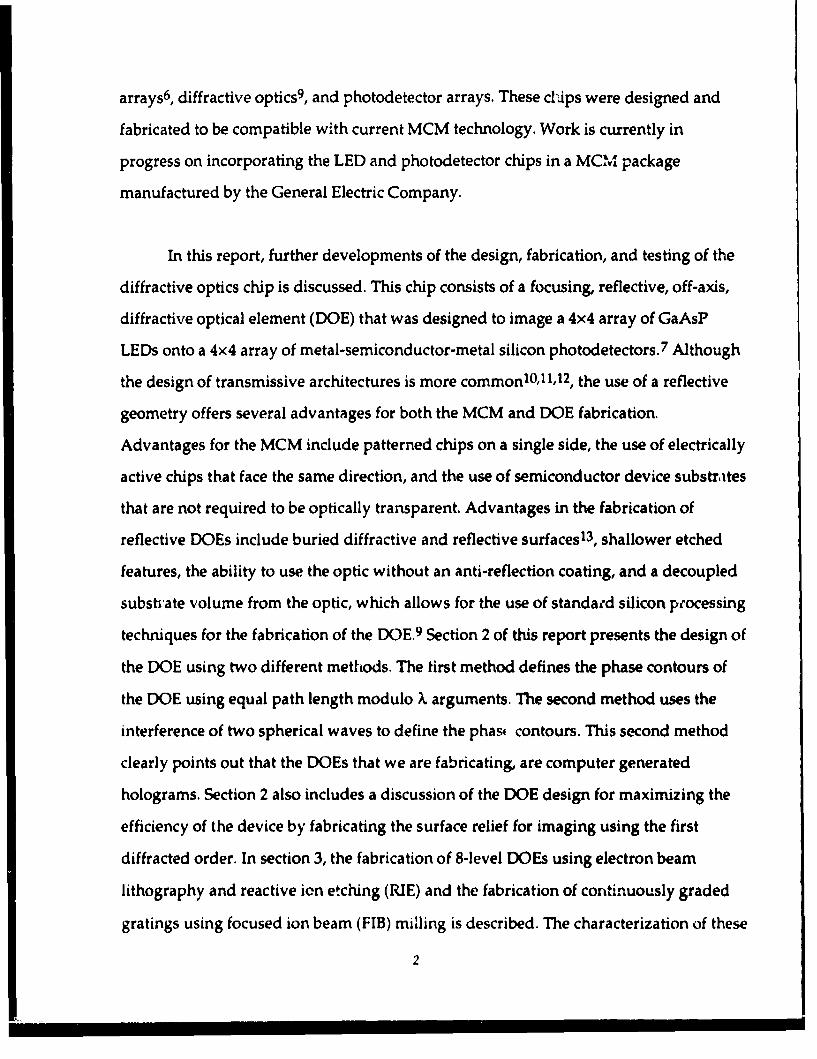
2.4. Effects on surface relief due to off-axis operation
For off-axis rays incident on the grating at an angle Owith respect to the grating
normal, the surface relief must be modified to account for the different optical path
lengths. This effect is displayed in figure 2.4 for two rays at a zone interface. For a
surface relief designed to operate in the first order, these two rays must have an optical
path difference (OPD) of X to interfere constructively. The surface relief h, is therefore
given by,
h=- (2.17)cos 0 +cos0'
where Od is the angle of diffraction. The surface relief will therefore be larger compared
to a relief designed for normal incidence.
13
Jh
Figure 2.4. Surface relief for off-axis rays. The sum of the OPDs mustequal X for constructive interference to occur, thereby determining thesurface relief.
14

3. Process development, fabrication, and characterization of DOEs using electron
beam lithography and reactive ion etching, and focused ion beam milling.
3.1. Process development and characterization of fabrication of DOEs using electron
beam lithography and reactive ion etching
3.1.1. Process overview
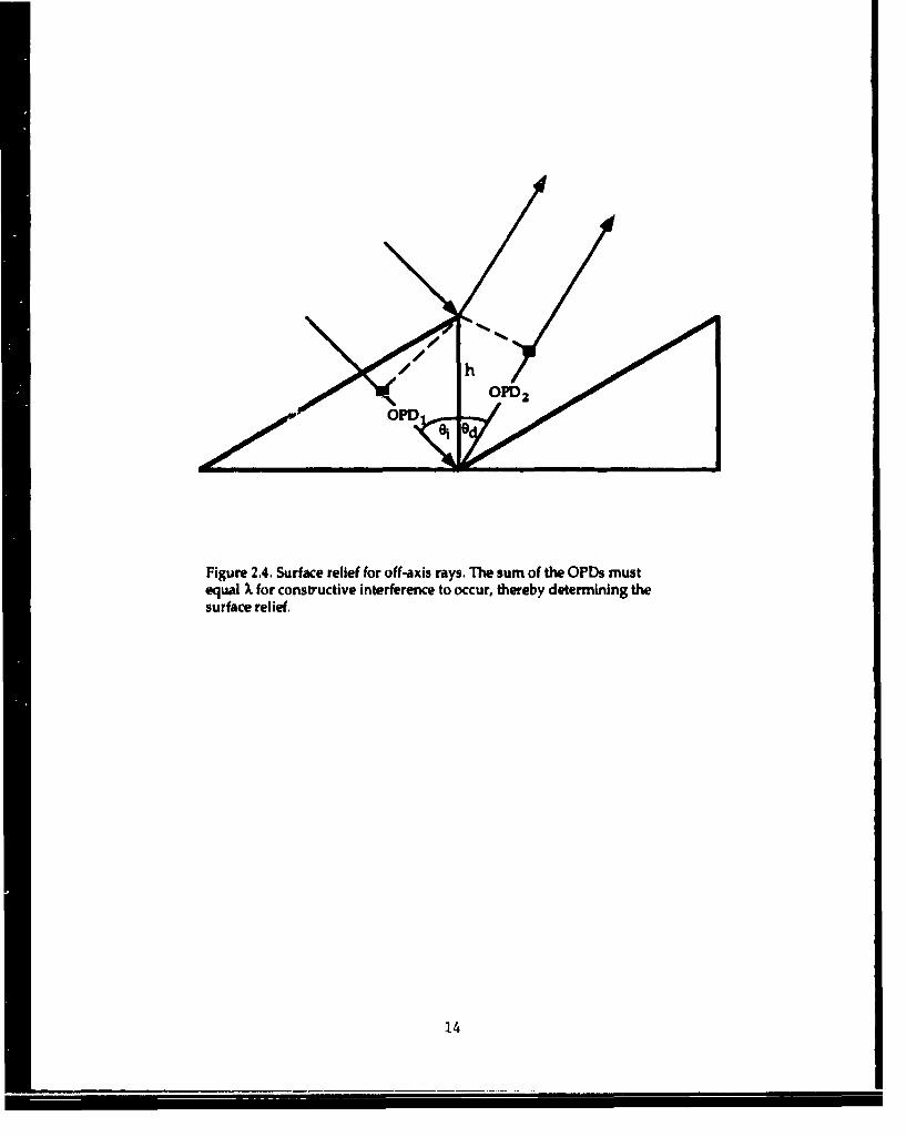
A schematic representation of the fabrication process is shown in figure 3.1. The
wafer is first prepared with global and local alignment marks. Alignment marks consist
of 4prm squares of lifted-off 1000A Pt and a 70A Cr adhesion layer. A 60nm film of
thermally evaporated SiOx is used to mask the wafer during the Si etch. Uniform SiOx
films with a minimum number of pinholes are generated by careful control of the input
power to the SiO source material. A 90nm PMMA resist layer is spun on and baked.
Phase contours are written by electron beam lithography at 20kV, a beam current of
2nA, a beam diameter of 100nm, and a field size of 0.8192mm 2 . The wafer is developed
in a solution of 1:1 MIBK:IPA. The developed phase contours are etched into the wafer
using a two step RIE process. The exposed pattern is transferred into the SiOx, using
CHF3 (30sccm) / 02 (2sccm) at 0.25W/cm 2 power and 3OmT chamber pressure. The
pattern is transferred from the SiOx to the Si wafer using BC13 (10sccm) /C1 2 (Ssccm) at
a sample bias of -100V and 20mT chamber pressure. The remaining oxide is stripped
using a 6:1 solution of buffered HF. This process is repeated once to generate a 4-level
DOE and twice to generate an 8-level DOE.
15
(a) electron beam exposure (d) BCI3/CI2 RIE
PMMA\9
(b) develop exposed resist (e) patterned Si after oxide strip
(c) CHF 3,0 2 RIE
Figure 3.1. Overview of fabrication process for diffractive optical element in Si.
16

3.1.2. Alignment marks
The intial round of processing consists of the fabrication of global and local
alignment marks on a 3" Si wafer. Global (wafer-level) alignment marks are used to
correct for errors in rotation and translation by the insertion of the wafer into the
electron beam lithography machine. Local alignment marks (field-level) are used to
precisely locate, rotate, and scale the electron beam lithography field where the patterns
are written.8 The layout and design of these marks are defined in the computer aided
design (CAD) program SYMBAD. Global alignment marks are generated by the
SYMBAD macro program GCA-KEY. A single global alignment mark is shown in figure
3.2. The 41im x 4pm square at the center of the arrows is the mark used by the electron
beam lithography machine for alignment, while the arrows are guides for the operator
to locate the center mark. 44m x 4pm squares are also used for local alignment marks.
The patterns generated in SYMBAD are converted into an intermediate data format,
Calma GDS-II using the SYMBGDS utility, and then converted into a binary pattern
data (BPD) format which is the exposable format for the Cambridge Instruments EBMF
10.5/CS electron beam lithography system used in this work. GDS files are converted to
BPD files using the Calma converter utility CALESF. 14 As described previously8 , the
DOE patterns are exposed in four overlapping quadrants. 4-point local field alignment
in each quadrant is used to align successive binary levels of the DOE. Three marks are
used for global alignment.
The lift-off process used to fabricate alignment marks is schematically displayed
in figure 3.3. The wafer is cleaned with a spin treatment of acetone and isopropyl
alcohol (IPA) and then spun dry. The wafer is baked at 170*C for 10min. The wafer is
then coated with a bi-layer resist. The first layer cokisists of a 6% P(MMA-MAA)
copolymer disolved in chlorobenzene. The copolymer solution is spun on at 1800rpm
17

Figure 3.2. CAD pattern of a global alignmert mark used to correct for rotationand translation errors at the wafer level.
18
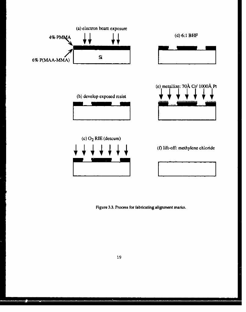
(a) electron beam exposure
4% PM%4A 4 (d) 6:1 BHF
6% P(MAA-MMAJ) 7 _1
(e) metallize: 70A, Cr/ IOOOA Pt
(b) develop exposed resist 4 ~ ~r
(c) 02 RIE (descum)
S(0 lift-off: methylene chloride
Figure 3.3. Process for fabricating alignment marks.
19

for 60sec and then baked at 170°C for 1hr. This produces a layer approximately 300nm
thick. The second layer consists of 4% PMMA that is spun onto the wafer at 4000rpm
for 60 seconds and then baked at 170°C for lhur. This thickness of the second layer is
approximately 240nm. Due to scattered electrons in the resist and backscattered
electrons from the oxide and substrate during exposure, and the relative sensitivities of
the two resists, an undercut profile occurs. This undercut profile is critical for lift-off.
The wafer is then loaded into the EBMF where the alignment marks described in the
previous paragraph are written in.o the bi-layer resist. EBMF parameters include a 20kV
accelerating potential, 2nA beam current, 100pC/cm 2 dose, and 0.8192mm 2 field sizes.
A single global alignment mark extends across 9, 0.8192mm 2 fields while a single set of
local marks are centered in a single 0.8192mm 2 field. Automatic electron beam
deflection, distortion, focus, and stigmation corrections are performed prior to the
exposure. Typical beam diameters range from 100nm to 150nm and typical distortion
errors across the field are less than 25nm or the linear dimension of one exposure
element. After exposure, the wafer is developed for 90sec in a 1:1 solution of MIBK:IPA,
rinsed in IPA, and blown dry. A 0.08min 02 plasma descum is performed in the PT-72
reactive ion etcher. Prior to loading the wafer into the etcher, a 5min 02 clean is
performed to remove contamination left from previous users of the machine. PT-72
etching parameters include a 30% 02 flow rate, a 20% RF power level, and a chamber
pressure of 60mT. Up to two wafers have been descummed simultaneously with no
evidence of detrimental loading effects. A wet etch using 6:1 buffered HF is performed
for 5min to remove the native oxide on the wafer. The wafer is subsequently rinsed in
de-ionized (DI) H 20. Evidence that the etch behaved correctly is displayed if the H 20
does not the wet the wafer surface. Native oxide formation should be prevented for
approximately lhr after this etch, so adequate time is available to perform the next
processing step, metal deposition. For metal deposition, a special 'lift-off' chuck is used
to hold the wafer. This chuck is radially symmetric about the electron beam source
20

material, thereby allowing metal atoms to strike the wafer normal to the surface. This is
critical for preventing metal from bridging across the overhang profile of the developed
resist, thereby preventing proper lift-off. 70A of Cr is thermally evaporated onto the
wafer for use as an adhesion layer for the 1000A Pt that is subsequently evaporated
using electron beam excitation. An evaporation rate of -1k/sec is used for the Cr and
-3A/sec for the Pt. The CVC SC4500 evaporator is used so that both thermal and
electron beam evaporations can be done in the same chamber, thereby maintaining a
vacuum between evaporations. The sample is allowed to cool for 15min between
evaporations. Once the wafer is unloaded from the evaporation chamber, it is placed in
a methylene chloride bath. The majority of the metal on the wafer immediately lifts-off,
leaving 1000A Pt alignment marks. A second bath of methylene chloride is used to
remove most of the remaining metal scum, and then the wafer is rinsed in an IPA bath
and blown dry. Further removal of mi-roscopic metal particles that were lifted-off and
then reattached can be accomplished by a spin rinse of methylene chloride, acetone, and
IPA.
3.1.3. Thin film SiO evaporation
The next step in the fabrication process is the evaporation of a 60nm film of SiO,
onto the Si wafer. The SiOx is used as an intermediate masking layer for the selective
etching of si.Ref Thermal evaporation is chosen over plasma enhanced chemical vapor
deposition (PECVD), since less pinholes in the film are generated and the oxide is less
conformal to previously patterned surface reliefs, thereby decreasing surface roughness
profile irregularities. The source material for the evaporation is crystalline SiO. In
previous reports8 a special chimney furnace was used to evaporate the SiO. The
chimney furnace was used to prevent solid particles, that are outgassed from the source
due to trapped water vapor, from embedding into the wafer, thereby ruining the quality
21

of the film. The power required to operate this furnace, however, is at the maximum
power capacity of the evaporation system. Therefore, a standard tungsten source boat
was tried, with the surprising result that high quality SiOx films were deposited, at
input powers well within the operating limits of the evaporation system. To deposit
high quality films of SiOx usin this method, the source must be thouroughly outgassed
before deposition can occur. The source current was increased at a rate of 1OA/min
until 150A was reached. The source was then stablilized at 150A for 7min and then
depostion was initiated.
3.1.4. DOE pattern definition and electron beam lithography
DOE phase contours are generated using the algorithms given in equations (2.2)
and (2.3) by FREDD. The conversion and subsequent data fracturing of these phase
contours to BPD format has previously been described. 8 Programs MODIFY8 and
POLY.FOR8 , which are used in the conversion process, have been modified according to
the particular application. Figure 3.4 displays one quadrant of a phase subzone, after
conversion and fracturing into BPD format. The primitive shapes shown in this figure
are individually addressed by the Cambridge EEMF. 2 million primitive shapes are
addressed for a 1mm diameter2-level DOE, 6 million primitive ipes are addressed
for a 4-level DOE, and 14 million primitive shapes for an 8-level DOE. Since 0.8192mm 2
field sizes are being used, the EBMF, using 15 bit digital-to-amalog converters, has the
ability to address these primitive shapes at 1.074x10 9 locations per quadrant, by using a
25nm pixel size. This makes pattern digitization unresolveably small, even for patterns
with large curvatures. Linear 2-, 4-, and 8-level gratings have also been generated in
SYMBAD and then written by electron beam lithography. These gratings are used as
test structures to test the efficiency of a specific local spatial frequency region of the
DOE, as well as monitor the ability to align successive multiple levels with submicron
22

Exels39000.0 39500.0 40000.0 40500.0 41000.0
39000.0 I I
39500.0"
40000.0-
............ ....
40500.0 -
41000.0
Figure 3.4. BPD data of a fractured subzone.
23

periods. All patterns are exposed at 2nA beam current.
3.1.5. Proximity effects on grating fabrication
To accurately align multiple levels of a DOE, not only must the alignment to
metal marks be precisely defined (typical accuracies on the order of 0.1gm), but the
electron beam dose must be correct to define 50% duty cycle lines and spaces. Due to
proximity effects caused by the scattering of secondary and backscattered electrons,
overexposure or underexposure can occur for a given combination of resist thickness,
oxide thickness, substrate type, and doping combination, if the electron beam dose is
not correctly calibrated. The effects of overexposure and underexposure on an 8-level
grating are displayed in figures 3.5a and 3.5b, respectively. To calibrate the dose, a
series of 50% duty cycle lines and spaces were written using a range of doses (40-
ll0giC/cm 2) while keeping other fabrication cunditions the same as the .ctual DOE,
including development and etching. Line and space widths were written in the range of
0.3 - 4.0gm, since this is the range of feature sizes used to fabricate the DOE. The
cuumalitive results for proximity effects over a range of period sizes is displayed in
figure 3.6. This data identifies 60g.C/cm 2 as the dose with the smallest pixel error (less
than one pixel) (ver the range of feature sizes used to fabricate the DOE. 8-level linear
gratings were fabricated at doses of 50,60, 70, and 80pC/cm 2. These linear gratings are
displayed in figure 3.7. As expected, 60gtC/cm 2 produces the best results, while for
80gtC/cm 2 trenches at step interfaces clearly display overexposure characteristics
(trenching) and similarly, underexposure effects are observed for a dose of 50tC/cm 2. It
should be noted that previously8S9, an in depth analysis, taking into account proximity
effects as well as the effects of transferring the developed pattern into the Si substrate
using RIE, was used to determine the ideal dose. Using fabrication procedures identical
to this work, a dose of 90tC/cm 2 was determined. This is significantly different from24

(a) (b)
I I
II III ,II IIII I
I ! I !III I III
I I'
i i I
J I
Figure 3.5. Schematic representation of the effects of (a) overexposure and (b) underexposureon the alignment of binary levels. The solid profiles are desired and the dashed profiles arethe result of proximity effects. The top figures are the resulting profiles after one etch and thebottom profiles are the profiles after two etches. For overexposure, trenches develop at stepinterfaces and for underexposure, mesas develop at step interfaces.
25

'1 " I ' *
S' ; ~0.3pro (81 nm) , .
-'---= O.S7.m (81)S 0.7gro ( 81 ) ,
40 - 0.911m (81)•r 2.Oro (01) •"
....... 0.3 rm (46nm)i '•~ ~~ ..... a .... 0.AIm (46) .," /..' ........ m .... O.Sgm (46),.. i,,
20 ...-*" O.9.gm (46)-20 . ..--- 2.Ogr (46) .. .....
.........* ' ° 0' q
4 ,.. ..° e....; .. .. .
S0
-0 .20
40 60 80 1O00
dose (gC/cm2)
Figure 3.6. % pixel error versus dose for DOZE feature siz'es. 60gC/cmn2 isidentified as the optimum dose since errors less than one pixel are observedover the range of feature sizes.
26

MIA~ a'

the ideal dose determined in this work, which signifies that slightly different
environmental conditions in the lab, as well as possibly different conditions of the
electron beam lithography machine (new filament, different machine calibrations) can
cause significantly different ideal exposure conditions. Therefore, dose calibrations for a
given process must be performed regularly. Using a high-resolution (2nm) field
emission SEM (Hitachi S800), a single period can be examined and is displayed in figure
3.8. This figure demonstrates the ablility to align multiple levels to within 50nm worse
case, and on the order of 2nm best case. 15 Also displayed in figure 3.8 are several
periods of this grating, demonstrating the uniformity of the fabrication. Such accurate
alignment allows us to fabricate highly efficient DOEs.
3.1.6. Reactive ion etching
The transfer of the exposed pattern from the SiOx to the Si wafer consists of a three
step RIE process using a Plasma Therm PK1250 reactive ion etcher. In the first step, a
45sec etch using BCI 3 (40sccm)/H2(20sccm) and a sample bias of -200V removes residual
water contamination on the substrate and carrier. In the second step, a 45sec etch using
C12 (5sccm)/BCl3 (40sccm)/ H2 (20sccm) and a sample bias of -300V removes the native
oxide on the exposed Si surfaces. Both of these steps occur at a chamber pressure of 20mT.
The Si is then patterned using BCI3/CI 2. For DOEs to be tested at the wavelength of
632.8nm (HeNe laser wavelength) etch depths of 160nm, 80nm and 40nm are required for
2-, 4-, and 8-levels respectively. An extensive series of etch test runs were performed to
determine flow rates, chamber pressures, and sample bias voltages required to achieve
the desired etch depths. The results of these etch tests are displayed in figure 3.9. To
determine the etch depth, after the sample is unloaded from the etcher, the remaining SiO
is stripped using 6:1 BHF (2 minute bath), dunked in a DI H20 bath, blown dry, and then
measured using a Tencor alpha-step. It is clear from figure 3.9 that the conditions that
28

I 44 I o i

150
11100
T a L12(40 sccnl/Ba 3 (5sccnj;20mT,-200V
50 C sccnt/BC33(Ssccnt;4moT,.IOOV
A C12(40 sccnj/BC 3 (5sccnj;20nT,-1OOVo 0 C12(20 scc0/BCl3 (5sccnj;20mT,-100V
- * C2(10 sccnj/BCi3 (Ssccn';20mT,.-0OV
0 1 2 3 4 5chlorine etch time (min)
Figure 3.9. Si etch depth versus etch time for different flow rates, chamber pressures,and sample biases. The solid line is a linear fit to the data for the etching conditionsmost suitable for the 8-level DOE.
30

produce the desired etch depths in the most well controlled manner are BC13
(10sccm)/Cl2 (5sccm) at a sample bias of -100V and a chamber pressure of 2OmT.
The data in figure 3.9 also indicates that the goal etch depths are repeatable to
within +/- 10nm. To determine the effect of the etch error on efficiency, equation (2.16) is
evaluated. Diffraction efficiency versus etch error is displayed in figure 3.10 for 4- and 8-
level binary surface reliefs. In this plot, etch error refers to the error of each etch for 4- or
8-level DOEs. For an 8-level DOE, a +/- 10nm variation in etch depth produces
efficiencies ranging from 95% to 77%, and for a 4-level DOE, 81% to 77%. This first order
calculation demonstrates that tight tolerances are required to achieve near theoretical
efficiencies for 8-level DOEs, with more relaxed requirements for 4-level DOEs. Since the
shallowest etch produces the largest percent phase error, it should be performed first, so
if necessary, subsequent etch depths can be adjusted to prevent the accumulation of
phase errors.
3.1.7. Characterization of grating etch depths using atomic force microscopy
To characterize the etch depth and surface profile of the grating, AFM is used,
since the alpha-step is not useful for submicron features. Area and line scans are
displayed in figure 3.11, for several periods of an 8-level linear grating fabricated at near
optimal conditions as described in sections 3.1.5 and 3.1.6. This grating was processed
by etching deep features first, and then etching subsequently shallwer features. For the
third and shallowest etch, a large deviation (20nm) occured in the etch depth producing
significant errors in the step heights of the grating shown in figure 3.11. Using equation
(2.16) a first order efficiency of 77.5% is expected and a non-zero zero'th order efficiency
of 2.3% is expected. Since the PK1250 is a mult-purpose machine that is used for etching
materials other than Si (i.e. GaAs), processes that use different gases than those used to
31

1.0 ''4 4-lev.l'......8-level
0.8
S0.6
O0.4
0.2
0.0 ......I . I , , . , I . . . .a I . . . . I , a
0 50 100 150 200
etch error (nm)
Figure 3.10. Diffraction efficiency versus etch error for 4- and 8-level binarysurface reliefs. For a 9,7nm etch error at each etch, the efficiencies for 4- and 8-levels are equal.
32

iI
ID IO2 6 8 ID t
2.5 5.0 7.5 10.0 iN
Figure 3.11. AFM surface profile (top) and line scan (bottom) of severalperiods of an 8-level linear grating fabricated at 604iC/cm 2.
33

etch Si, (i.e. argon and methane) can produce contamination of the chamber, thereby
changing the etch rate. A cleaning step should therefore be included in the process,
possibly using the gas mixture of the first etch step, without the sample loaded into the
chamber.
3.2. Process development and characterization of DOEs fabricated by focused ion
beam milling
A 69Ga+ focused ion beam is used to sputter continuously graded gratings.16,17
The linearly blazed surface relief is milled in a single lithography step by linearly
varying the sputter yield across a given period. The linear variation in sputter yield is
produced by a linear variation in area dose of the ion beam. For a reflection grating
designed to operate at X=632.8nm with 4gm wide periods, the area doses used to
produce surface reliefs of X/2 range from 4x10 16 to 641017 ions/cm 2. For a given area
dose, the FIB is raster scanned the length of the grating using a 22.5nm square pixel size.
The beam diameter is sub-tenth micron and the beam energy is 6OkeV. To account for
the effects of redeposition of material and beam profile, a pattern scheme of 8
overlapping area doses within a given period is used. AFM is used to characterize the
surface relief profile. AFM surface and line scans are shown in figure 3.12. Since binary
surface relief profiles are only an approximation to a continuous blaze, FIB gratings can
potentially produce superior diffraction efficiencies. The fabrication of a continuously
graded surface relief by FIB milling, also suggests that diffractive optical elements with
binary surface profiles or surface profiles with inaccuracies due to fabrication errors,
such as the grating described in section 3.1.7 can be repaired and rendered continuous
by FIB milling, thereby producing high-quality surface masters. For our particular FIB
system, pattern write times can be prohibitive (a 481•mx481m grating was written in
1.7hrs), thereby limiting the fabrication to very small areas, or the repair of slightly
34

ii
2 4 6 8 10 •
SI I I- H -0 2.5 5.0 7.5 i0.0 im
Figure 3.12. AFM surface profile (top) and line scan (bottom) of severalperiods of a continuously blazed grating fabricated using focused ionbeam milling.
35

larger areas. Other FIB systems18 , however, have write times that are faster by factors of
10, thereby potentially realizing the ability to fabricate bigh-quality diffractive optic
masters.
36

4. Device performance
The zero'th and first order diffraction pattern for the 8-level linear grating
(60g.C/cm 2) is shown in figure 4.1. The relative efficiency (taking into account the
reflectivity of the Si) of the first order is 75% and for the zero'th order, 6%. As expected
from the analysis in section 3.1.7, the efficiency of the first order diffraction is less than
theoretical (95%) and is slightly less than the calculated efficiency using the surface
profile data (77.5%.) Additional losses in efficiency may be due to the overall roughness
of the grating, non-uniformities in grating period across the grating area, and
subwavelength feature sizes. Since etch depth errors dominate the reduction in
efficiency, these additional effects are difficult to quantitatively analyze.
37

+1 order
150.0
• 100.0
500
1.025.0 97.0
49.0 73.073.0 49.0
Y (arb. units) 97.0 X (arb.unita)1.0
Figure 4.1. Rendered CCD image of diffraction pattern of the 8-level lineargrating described in text.
38

S. Conclusions and ongoing work
2-, 4-, and 8-level off-axis DOEs and linear gratings have been designed and
fabricated. Fabrication techniques include electron beam lithography and RIE.
Continuously graded, blazed, linear gratings have been fabricated using FIB milling.
The quality of the fabrication has been characterized using SEM and AFM. 8-level linear
gratings have been tested with efficiencies of 75%. Although 8-level gratings have not
been fabricated with near theoretical efficiencies (greater than 90%), procedures have
been developed and discussed for fabricating highly-efficient devices.
Ongoing work includes fabricating higher efficiency devices, developing
measurement techniques for measuring intensity profiles and efficiencies of the
fabricated off-axis reflecting DOEs, and measuring system performances, including
cross-talk, of a free-space optical interconnect.
39
6. References
1. M.R. Feldman, S.C. Esener, C.C. Guest, and S.H. Lee, "Comparison between opticaland electrical interconnects based on power and speed considerations," AppI. Opt. 27,1742 (1988).
2. Edward G. Myszka, Allison Casey Dixon, and Jim Trent, "A multichip package forhigh-speed logic die," IEEE Trans. on Components, Hybrids, and Manufacturing Tech.16.1, 66 (1988).
3. J.W. Goodman, F.J. Leonberger, S.Y. Kung, and R.A. Athale, "Optical interconnectionsfor VLSI systems," Proc. IEEE 72, 850 (1984).
4. Ray T. Chen, Huey Lu, Daniel Robinson, Michael Wang, Gajendra Savant, andTomasz Jannson, "Guided-wave planar optical interconnects using highly multiplexedpolymer waveguide holograms," IEEE J. Lightwave Technol. 10.7, 888 (1992).
5. D.A. Honey, F. Haas, H. Bare, H.G. Craighead, S.M. Shank, S.S. O'Keefe, W.J. Schaff,and L.F. Eastman, "Optical interconnects for wafer-scale integration," SPIE InternationalSymposium on Optical Engineering in Aerospace Sensing 2216 (1994).
6. H.F. Bare, F. Haas, D.A. Honey, D. Mikolas, H.G. Craighead, G. Pugh, and R. Soave,"A simple surface emitting LED useful for developing a free-space opticalinterconnect," IEEE Photon. Technol. Lett. 5, 172 (1991).
7. H.G. Craighead, D. Mikolas, F. Haas, D.A. Honey, and H.F. Bare, "Free-space verticaloptical interconnect using reflective binary optic focusing gratings and arrays of LEDsand photodetectors," Final Technical Report RL-TR-93-116 (1993).
8. D. Mikolas and H.G. Craighead, "Development of a vertical optical interconnect,"Final Technical Report RL-TR-93-167 (1993).
9. D. Mikolas, R. Bojko, H.G. Craighead, F. Haas, D. Honey, and H.F. Bare, "Fabricationof aspheric high numerical aperature reflective diffractive optic elements using electronbeam lithography," J. Vac. Sci. Technol. B12, 20 (1994).
10. Shigura Kawai, "Free-space multistage optical interconnection networks using microlens arrays," IEEE J. Lightwave Technol. 9, 1774 (1991).
11. Michael W. Haney and James J. Levy, "Optically efficient free-space folded perfectshuffle network," Appl. Opt. 30,2833 (1991).
12. Bart Dhoedt, Peter De Dobbelaere, Lue Buydeus, Roel Baets, and Bruno Houssay,"Optical free-space board-to-board interconnect: options for optical pathways, Appl.Opt. 31, 5508 (1992).
40

13. Teruhiro Shiono and Hisahito Ogawa, "Diffraction-limited blazed reflectiondiffractive microlenses for oblique incidence fabricated by electron beam lithography,"Appl. Opt. 30,3643 (1991).
14. Richard J. Bojko, "Cambridge Instruments EBMF 10.5/CS Electron BeamLithography System - Users Manual," (1991).
15. S. M. Shank and H.G. Craighead, "Binary optics for optical interconnects," SPIEInternational Symposium on Optical Engineering in Aerospace Sensing 2216 (1994).
16. S.M. Shank, M. Skvarla, F.T. Chen, H.G. Craighead, P. Cook, R. Bussjager, F. Haas,and D.A. Honey, "Multiple-level phase gratings fabricated using focused ion beammilling and electron beam lithography," to be presented at the 38th InternationalSymposium on Electron, Ion and Photon Beams (1994).
17. S.M. Shank, M. Skvarla, F.T. Chen, H.G. Craighead, P. Cook, R. Bussjager, F. Haas,and D.A. Honey, "Fabrication of multi-level phase gratings using focused ion beammilling and electron beam lithography," to be presented at the Diffractive Optics:Design, Fabrication and Applications Topical Meeting (1994).
18. Y. Ochiai, K. Shihoyama, T. Shiokawa, K. Toyoda, A. Masuyama, K. Gamo, and S.Namba, J. Vac. Sci. Technol. B4, 333 (1986).
6U,5, GOVERNMENT PRINTING OFFICE 1994-610-1;16-50178
41.
![20110228252 - apps.dtic.mil · However the effect of sintering was found to be minimal by previous research[l]. Composition[% Wt. Ag] Saturation sulfur capacity [mgS/g] Active metal](https://img.pdfslide.net/doc/110x75/60ee9d9f91a443292c079fb4/20110228252-appsdticmil-however-the-effect-of-sintering-was-found-to-be-minimal.jpg)