Embed Size (px)
DESCRIPTION
pcb
Citation preview

Home Products Noise Suppression Products / EMI Suppression Filters / ESD Protection Devices EMI Suppression Filters Noise Suppression Techniques Noise Suppression Basic Course Chapter05-P2
Global English News Investor Relations Careers Contact us
Type to Search
Products Applications Design Tools Support About Murata my Murata
Noise Suppression Products/EMI Suppression Filters
Chapter 1
Chapter 2
Chapter 3
Chapter 4
Chapter 5
Chapter 6
Chapter 7
Chapter 8
Chapter 9
Chapter 10
Chapter 11
Chapter 12
Chapter 13
Introduction5-1.
Conductor conductionof noise
5-2.
Common mode noiseoccurrence
5-3.
Summary of Chapter 55-4.
Chapter 5
Conductor conduction and common mode
5-3. Common mode noise occurrence
As described in Section 5-2, there is a normal mode and a common mode in components whennoise is transmitted through a cable. It was also shown that the occurrence of noise voltage, aswell as, the flow of noise current in the ground of an electronic device is called common modenoise. In this section, we will focus on noise occurrence in this ground and study some of the mechanismsthat generate common mode noise. The mechanisms that generate common mode noise in actual electronic devices are complex.Therefore, they cannot be explained with simple models such as these. The models introducedhere include elements with complex numerical values, such as floating electrostatic capacitance,so they are difficult to incorporate into a design. However, understanding such mechanisms is very useful in designing low-noise electronic devices.
5-3-1. Examples of common mode noise occurrence
(1) When a cable is attached to the ground of a clock signal
Fig. 5-3-1 shows that noise emission is measured when a 20MHz clock signal is transmittedthrough a 5cm MSL (Micro Strip Line) at a frequency range of 30MHz to 1GHz and at a distance of3m. Fig. 5-3-1(a) shows the result of using only a substrate while Fig. 5-3-1(b) shows the result ofattaching two 25cm cables to the ground. We can conclude that when a cable is attached to theground, noise emission increases to a frequency in which the entire wavelength nearly becomeshalf (in this case, 250MHz). Therefore, we can say that attaching a conductor, such as an antenna, to the ground of a PCB,increases the noise, which is the same as the condition shown in Fig. 5-2-2 of Section 5-2. In otherwords, you can think of common mode noise as being induced by this ground. (The test in Fig. 1 uses a substrate which has a ground on both sides of the MSL. This is not thestructure of a regular MSL. Nonetheless, this section refers to it as MSL.)
(2) MSL also has noise in the ground
In this test, a clock signal is generated in an oscillator circuit housed in a small 3cm × 3cm shieldingcase using a built-in 3V battery, in order to neutralize the effects of noise emission from partsother than the cable and MSL. The device's appearance is shown in Fig. 5-3-1(c). This signalgenerator is also used as a noise source in succeeding tests. Incidentally, the MSL used here is similar to the ideal signal wiring. As the figure shows, the frontand back of the substrate becomes the ground plane connected through via, which is primarily forpreventing voltage occurrence in the ground. Is it fine to assume that this noise was generated bythis kind of mechanism? Also, how can it be suppressed?
converted by Web2PDFConvert.com
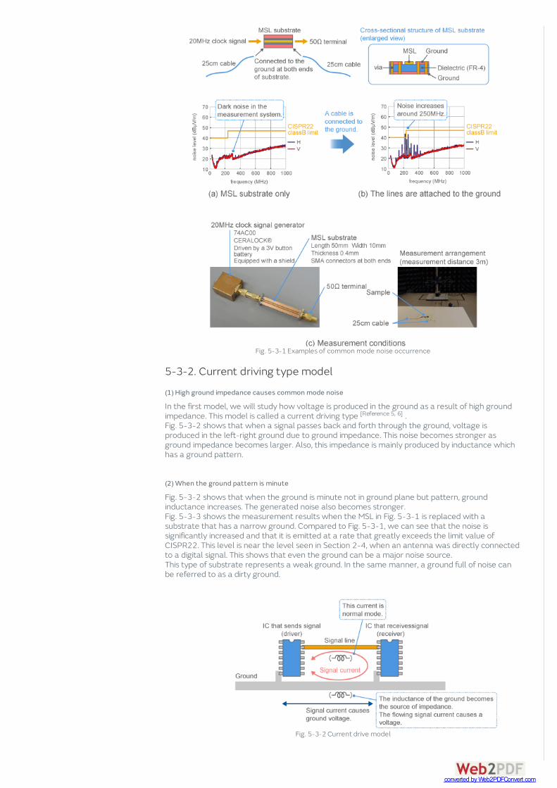
Fig. 5-3-1 Examples of common mode noise occurrence
5-3-2. Current driving type model
(1) High ground impedance causes common mode noise
In the first model, we will study how voltage is produced in the ground as a result of high groundimpedance. This model is called a current driving type . Fig. 5-3-2 shows that when a signal passes back and forth through the ground, voltage isproduced in the left-right ground due to ground impedance. This noise becomes stronger asground impedance becomes larger. Also, this impedance is mainly produced by inductance whichhas a ground pattern.
(2) When the ground pattern is minute
Fig. 5-3-2 shows that when the ground is minute not in ground plane but pattern, groundinductance increases. The generated noise also becomes stronger. Fig. 5-3-3 shows the measurement results when the MSL in Fig. 5-3-1 is replaced with asubstrate that has a narrow ground. Compared to Fig. 5-3-1, we can see that the noise issignificantly increased and that it is emitted at a rate that greatly exceeds the limit value ofCISPR22. This level is near the level seen in Section 2-4, when an antenna was directly connectedto a digital signal. This shows that even the ground can be a major noise source. This type of substrate represents a weak ground. In the same manner, a ground full of noise canbe referred to as a dirty ground.
Fig. 5-3-2 Current drive model
[Reference 5, 6]
converted by Web2PDFConvert.com
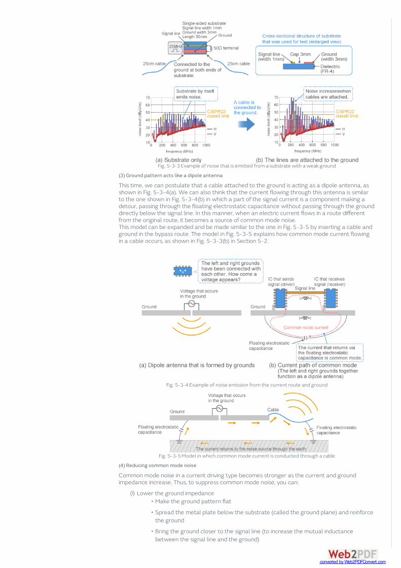
Fig. 5-3-3 Example of noise that is emitted from a substrate with a weak ground
(3) Ground pattern acts like a dipole antenna
This time, we can postulate that a cable attached to the ground is acting as a dipole antenna, asshown in Fig. 5-3-4(a). We can also think that the current flowing through this antenna is similarto the one shown in Fig. 5-3-4(b) in which a part of the signal current is a component making adetour, passing through the floating electrostatic capacitance without passing through the grounddirectly below the signal line. In this manner, when an electric current flows in a route differentfrom the original route, it becomes a source of common mode noise. This model can be expanded and be made similar to the one in Fig. 5-3-5 by inserting a cable andground in the bypass route. The model in Fig. 5-3-5 explains how common mode current flowingin a cable occurs, as shown in Fig. 5-3-3(b) in Section 5-2.
Fig. 5-3-4 Example of noise emission from the current route and ground
Fig. 5-3-5 Model in which common mode current is conducted through a cable
(4) Reducing common mode noise
Common mode noise in a current driving type becomes stronger as the current and groundimpedance increase. Thus, to suppress common mode noise, you can:
Lower the ground impedance(i)Make the ground pattern flat•
Spread the metal plate below the substrate (called the ground plane) and reinforcethe ground
•
Bring the ground closer to the signal line (to increase the mutual inductancebetween the signal line and the ground)
•
converted by Web2PDFConvert.com

The measures described in (i) point to ground strengthening. However, as shown in the sample test in Fig. 5-3-1, a small amount of common mode noise willstill be produced even when using an MSL that has a steady ground plane under the signal line.This is because there will be a minute inductance as long you don't have an infinitely large groundsurface.
5-3-3. Voltage driving type model
(1) When noise occurs even when there is no flowing current
In the current driving type model, voltage is produced due to current flowing through the ground.Therefore, one might assume that noise should not occur when there is no flowing current. In anactual electronic device, however, the reality is that common mode noise frequently occurs even ifthere is nothing connected before the signal line. In other words, noise is produced just by applyingvoltage to the signal line even if there is no current flowing. As an example, the test in Fig. 5-3-1 removes the load (50 ohms terminal). The change in noisewhen current is prevented from flowing through the signal line is shown in Fig. 5-3-6. (a) showsthe condition with a load and (b) shows the condition without a load. When there is no load, noisedecreases. However, a 220MHz noise remains. This cannot be clearly explained by the currentdriving type model.
Fig. 5-3-6 Example of noise produced despite the absence of a current
(2) Common mode current flows through the floating electrostatic capacitance
The remaining noise can be explained by the voltage driving type model. The voltage driving typeis simplified and described in Fig. 5-3-7 . When two parallel conductors are connected to the noise source, the part with the sameconductor length becomes the transmission line. A small amount of current flows through floatingelectrostatic capacitance C in between the lines, even if there is nothing connected before theconductors. However, since this current is in normal mode, noise emission is decreased. However, if one of the conductors is made longer, half of the voltage of the noise source is appliedto this conductor. This would create a type of dipole antenna with the other conductor. Thevoltage driving type model allows an antenna to be created using conductors protruding from thetransmission line in this manner. This time, the current which flows in the antenna flows through floating electrostatic capacitanceC , as shown in the figure.
Shorten the ground (to shorten the route of the feedback current, inevitablyshortening the signal line)
•
Reduce the electric current(ii)Increase the load impedance•
Cut unwanted high frequency range components using a filter•
[Reference 5,6]
DM
ant
converted by Web2PDFConvert.com
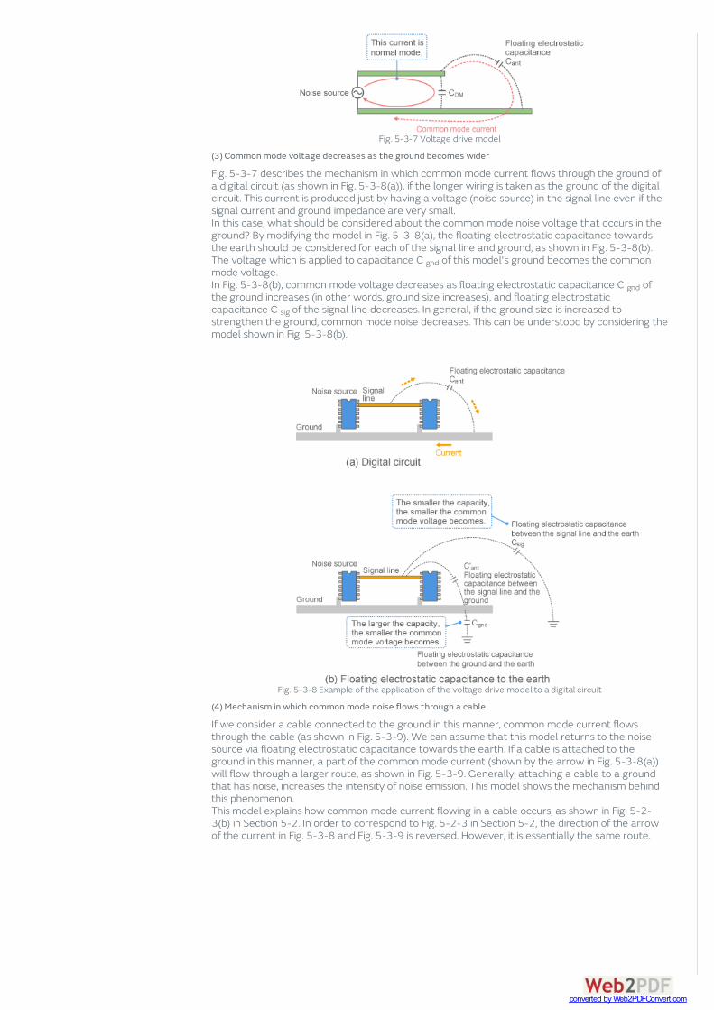
Fig. 5-3-7 Voltage drive model
(3) Common mode voltage decreases as the ground becomes wider
Fig. 5-3-7 describes the mechanism in which common mode current flows through the ground ofa digital circuit (as shown in Fig. 5-3-8(a)), if the longer wiring is taken as the ground of the digitalcircuit. This current is produced just by having a voltage (noise source) in the signal line even if thesignal current and ground impedance are very small. In this case, what should be considered about the common mode noise voltage that occurs in theground? By modifying the model in Fig. 5-3-8(a), the floating electrostatic capacitance towardsthe earth should be considered for each of the signal line and ground, as shown in Fig. 5-3-8(b).The voltage which is applied to capacitance C of this model's ground becomes the commonmode voltage. In Fig. 5-3-8(b), common mode voltage decreases as floating electrostatic capacitance C ofthe ground increases (in other words, ground size increases), and floating electrostaticcapacitance C of the signal line decreases. In general, if the ground size is increased tostrengthen the ground, common mode noise decreases. This can be understood by considering themodel shown in Fig. 5-3-8(b).
Fig. 5-3-8 Example of the application of the voltage drive model to a digital circuit
(4) Mechanism in which common mode noise flows through a cable
If we consider a cable connected to the ground in this manner, common mode current flowsthrough the cable (as shown in Fig. 5-3-9). We can assume that this model returns to the noisesource via floating electrostatic capacitance towards the earth. If a cable is attached to theground in this manner, a part of the common mode current (shown by the arrow in Fig. 5-3-8(a))will flow through a larger route, as shown in Fig. 5-3-9. Generally, attaching a cable to a groundthat has noise, increases the intensity of noise emission. This model shows the mechanism behindthis phenomenon. This model explains how common mode current flowing in a cable occurs, as shown in Fig. 5-2-3(b) in Section 5-2. In order to correspond to Fig. 5-2-3 in Section 5-2, the direction of the arrowof the current in Fig. 5-3-8 and Fig. 5-3-9 is reversed. However, it is essentially the same route.
gnd
gnd
sig
converted by Web2PDFConvert.com
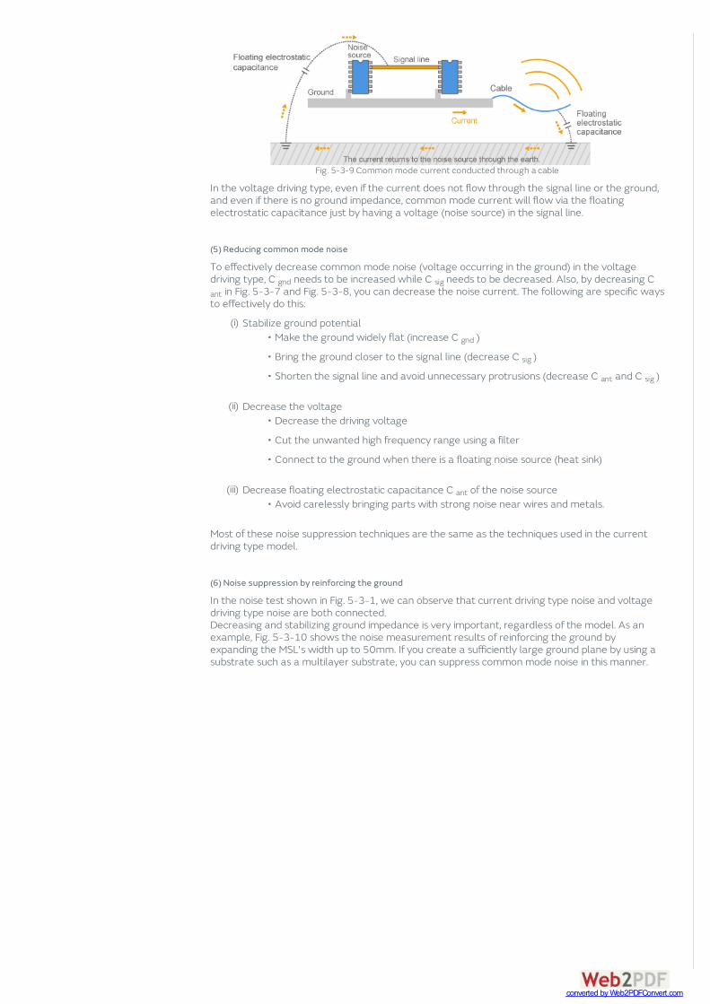
Fig. 5-3-9 Common mode current conducted through a cable
In the voltage driving type, even if the current does not flow through the signal line or the ground,and even if there is no ground impedance, common mode current will flow via the floatingelectrostatic capacitance just by having a voltage (noise source) in the signal line.
(5) Reducing common mode noise
To effectively decrease common mode noise (voltage occurring in the ground) in the voltagedriving type, C needs to be increased while C needs to be decreased. Also, by decreasing C
in Fig. 5-3-7 and Fig. 5-3-8, you can decrease the noise current. The following are specific waysto effectively do this:
Most of these noise suppression techniques are the same as the techniques used in the currentdriving type model.
(6) Noise suppression by reinforcing the ground
In the noise test shown in Fig. 5-3-1, we can observe that current driving type noise and voltagedriving type noise are both connected. Decreasing and stabilizing ground impedance is very important, regardless of the model. As anexample, Fig. 5-3-10 shows the noise measurement results of reinforcing the ground byexpanding the MSL's width up to 50mm. If you create a sufficiently large ground plane by using asubstrate such as a multilayer substrate, you can suppress common mode noise in this manner.
gnd sigant
Stabilize ground potential(i)Make the ground widely flat (increase C )• gnd
Bring the ground closer to the signal line (decrease C )• sig
Shorten the signal line and avoid unnecessary protrusions (decrease C and C )• ant sig
Decrease the voltage(ii)Decrease the driving voltage•
Cut the unwanted high frequency range using a filter•
Connect to the ground when there is a floating noise source (heat sink)•
Decrease floating electrostatic capacitance C of the noise source(iii) antAvoid carelessly bringing parts with strong noise near wires and metals.•
converted by Web2PDFConvert.com

Fig. 5-3-10 Suppressing common mode noise by reinforcing the ground
(7) Noise suppression using a EMI suppression filter
You can also suppress common mode noise by eliminating noise using an appropriate EMIsuppression filter, even substrates with a weak ground. Fig. 5-3-11 shows an example of using a π -type EMI suppression filter in the clock signal (noisesource) using the substrate with a weak ground used in Fig. 5-3-3. Although this filter is for normalmode, you can effectively suppress common mode noise by placing it right after the noise source(before conversion to common mode). In doing this, you must decrease the impedance of theground between the noise source and the filter as much as possible. For this test, MSL is used onlyin between the noise source and the filter. If you can find the noise source this way in an actual electronic device, you will be able to applynoise suppression using a normal mode EMI suppression filter, even if the substrate has a weakground.
Fig. 5-3-11 Noise suppression using a filter in a substrate with a weak ground
5-3-4. Ground structure to be considered
(1) Ground with low common mode noise
To reduce common mode noise due to the current driving model, it is important to reduce theground impedance so that the signal feedback current flows smoothly. Extra care is required inparticular for ground where feedback current flows through signals that contain high frequencycomponents such as clock signals. This section outlines some examples of ground structures thatcause many problems . Fig. 5-3-12(a) is an example of an ideal ground with low noise. Creating a ground plane beneaththe signal line as shown in the figure allows the signal feedback current to go back immediatelybelow the signal line, which reduces common mode noise. The ground plane covers the entire IC,not just the signal line. Note that the ground plane is shown in the figure, however in a multilayer substrate, the powerplane and ground plane operates in the same way. In the following examples where noise is
[Reference 7]
converted by Web2PDFConvert.com
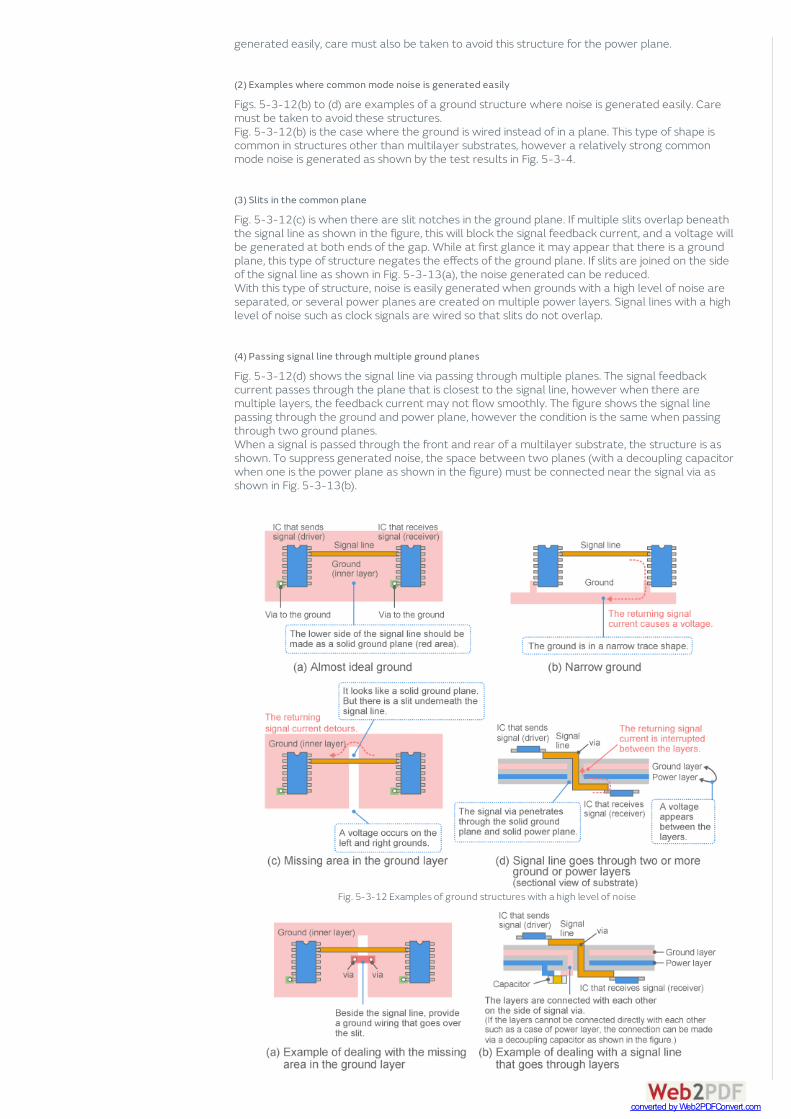
generated easily, care must also be taken to avoid this structure for the power plane.
(2) Examples where common mode noise is generated easily
Figs. 5-3-12(b) to (d) are examples of a ground structure where noise is generated easily. Caremust be taken to avoid these structures. Fig. 5-3-12(b) is the case where the ground is wired instead of in a plane. This type of shape iscommon in structures other than multilayer substrates, however a relatively strong commonmode noise is generated as shown by the test results in Fig. 5-3-4.
(3) Slits in the common plane
Fig. 5-3-12(c) is when there are slit notches in the ground plane. If multiple slits overlap beneaththe signal line as shown in the figure, this will block the signal feedback current, and a voltage willbe generated at both ends of the gap. While at first glance it may appear that there is a groundplane, this type of structure negates the effects of the ground plane. If slits are joined on the sideof the signal line as shown in Fig. 5-3-13(a), the noise generated can be reduced. With this type of structure, noise is easily generated when grounds with a high level of noise areseparated, or several power planes are created on multiple power layers. Signal lines with a highlevel of noise such as clock signals are wired so that slits do not overlap.
(4) Passing signal line through multiple ground planes
Fig. 5-3-12(d) shows the signal line via passing through multiple planes. The signal feedbackcurrent passes through the plane that is closest to the signal line, however when there aremultiple layers, the feedback current may not flow smoothly. The figure shows the signal linepassing through the ground and power plane, however the condition is the same when passingthrough two ground planes. When a signal is passed through the front and rear of a multilayer substrate, the structure is asshown. To suppress generated noise, the space between two planes (with a decoupling capacitorwhen one is the power plane as shown in the figure) must be connected near the signal via asshown in Fig. 5-3-13(b).
Fig. 5-3-12 Examples of ground structures with a high level of noise
converted by Web2PDFConvert.com
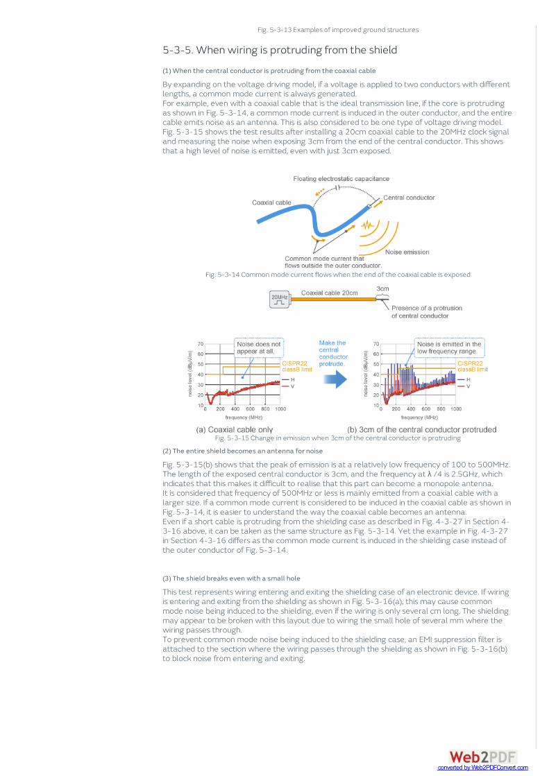
Fig. 5-3-13 Examples of improved ground structures
5-3-5. When wiring is protruding from the shield
(1) When the central conductor is protruding from the coaxial cable
By expanding on the voltage driving model, if a voltage is applied to two conductors with differentlengths, a common mode current is always generated. For example, even with a coaxial cable that is the ideal transmission line, if the core is protrudingas shown in Fig. 5-3-14, a common mode current is induced in the outer conductor, and the entirecable emits noise as an antenna. This is also considered to be one type of voltage driving model. Fig. 5-3-15 shows the test results after installing a 20cm coaxial cable to the 20MHz clock signaland measuring the noise when exposing 3cm from the end of the central conductor. This showsthat a high level of noise is emitted, even with just 3cm exposed.
Fig. 5-3-14 Common mode current flows when the end of the coaxial cable is exposed
Fig. 5-3-15 Change in emission when 3cm of the central conductor is protruding
(2) The entire shield becomes an antenna for noise
Fig. 5-3-15(b) shows that the peak of emission is at a relatively low frequency of 100 to 500MHz.The length of the exposed central conductor is 3cm, and the frequency at λ /4 is 2.5GHz, whichindicates that this makes it difficult to realise that this part can become a monopole antenna. It is considered that frequency of 500MHz or less is mainly emitted from a coaxial cable with alarger size. If a common mode current is considered to be induced in the coaxial cable as shown inFig. 5-3-14, it is easier to understand the way the coaxial cable becomes an antenna. Even if a short cable is protruding from the shielding case as described in Fig. 4-3-27 in Section 4-3-16 above, it can be taken as the same structure as Fig. 5-3-14. Yet the example in Fig. 4-3-27in Section 4-3-16 differs as the common mode current is induced in the shielding case instead ofthe outer conductor of Fig. 5-3-14.
(3) The shield breaks even with a small hole
This test represents wiring entering and exiting the shielding case of an electronic device. If wiringis entering and exiting from the shielding as shown in Fig. 5-3-16(a), this may cause commonmode noise being induced to the shielding, even if the wiring is only several cm long. The shieldingmay appear to be broken with this layout due to wiring the small hole of several mm where thewiring passes through. To prevent common mode noise being induced to the shielding case, an EMI suppression filter isattached to the section where the wiring passes through the shielding as shown in Fig. 5-3-16(b)to block noise from entering and exiting.
converted by Web2PDFConvert.com

Fig. 5-3-16 Broken shielding due to wiring passing through
5-3-6. Common impedance noise
(1) Interference between circuits due to common impedance
Power and ground is shared between multiple circuits within an electrical circuit. While it is idealthat this power and ground wiring have zero impedance, in reality they actually have very smallimpedance. Common impedance noise is where the impedance in common areascauses the current in part of the circuit to affect other circuits. This common impedance noise isalso one type of common mode noise model. This differs from the current driving model above asthere are multiple circuits, impedance other than inductance is taken into account, and containslines other than the ground. For example, in Fig. 5-3-17, power is supplied from the left side of the figure to operate circuit 1and circuit 2. The power and ground wiring are common for both circuit 1 and circuit 2, and have acommon impedance Zp and Zg. When a large current flows through circuit 1, the power and ground voltage change due to a dropin voltage caused by the common impedance. Common mode noise is generated in the circuit 2ground and cables connected to this ground as a result. In the figure, circuit 1 is defined as the source of noise, however common impedance noise isgenerated under the same effects even if circuit 2 is operating. In this case, noise is transmittedfrom circuit 2 to circuit 1.
Fig. 5-3-17 Common impedance noise
(2) Reducing common impedance noise
There are several methods that are effective for reducing common impedance noise, as shown inFig. 5-3-18, and include:
(a) has the same effect of suppressing noise as the current driving model shown in Section 5-3-2above.
(3) Use independent wiring for power and ground for each circuit
(b) is a method that uses the power supply point as the reference point, and then featuresseparate ground and power wiring connected to each individual circuit. There is no commonwiring, which eliminates common impedance noise. For example, when there are circuits that require large currents to be controlled, such as themotor driving circuit, combined with electronic circuits that operate on weak signals, this conceptcalls for separate power and ground to be used.
[Reference 2]
Use larger wiring to reduce impedance in common areas(a)
Use independent wiring for power and ground for each circuit to eliminate common areas(b)
Confine the circuit 1 current using a decoupling capacitor(c)
converted by Web2PDFConvert.com

(4) Single point ground
In method (b), the ground line is wired from the reference point to each terminal circuit, and isreferred to as a single point ground (more accurately, it is a single point ground due to the parallelconnection). This is a design guide that is used for analog circuits with relatively low frequencies. In addition to reducing the common impedance noise above, a single point ground is also effectivein preventing incorrect operation due to the potential difference of the terminal. Please refer totechnical books for more details on single point ground. A single point ground requires a large amount of wiring, which means that the wiring thicknessdecreases due to restrictions in area when creating the PCB as shown in Fig. 5-3-18(b). This inturn leads to an increase in impedance at the high frequency range. Additionally, whentransmitting a signal across circuits (for example, from circuit 1 to circuit 2), the design of theground, which is the signal return path, is difficult. For this reason, this method is not used veryoften with digital circuits.
(5) Decoupling capacitor
Fig. 5-3-18(c) outlines the method using a decoupling capacitor for the power source.Interference on circuit 2 can be prevented by confining a high frequency range current betweencircuit 1 and the decoupling capacitor. The decoupling capacitor is an effective method in the high frequency range that the capacitoroperates in. To increase the lower limit of the effective frequency, the electrostatic capacitance ofthe capacitor is increased. To reduce common impedance noise in digital circuits, a decoupling capacitor is generally usedafter reducing the impedance of the ground by increasing the thickness of the wiring as shown inFig. 5-3-18(a).
Fig. 5-3-18 Reducing common impedance noise
5-3-7. Connecting transmission lines with different levels of balancing
(1) Balanced circuit and unbalanced circuit
Until now, the ground has been described as mainly the voltage reference point, however in anunbalanced circuit such as a digital circuit, the ground also operates as the return path for thesignal current. In general, transmission lines carrying signals consist of balanced circuits and unbalanced circuits.These two circuits differ in the way the voltage is distributed relative to ground as shown in Fig. 5-3-19. Fig. 5-3-19 shows the distribution of voltage to ground when the line voltage is 1V. In (a) balancedcircuit, 0.5V voltages have been applied to each line, and the symbols are opposite. In contrast, (b)unbalanced circuit has 0V applied to the outer conductor and 1V to the central conductor. Asindicated, the characteristic of an unbalanced circuit is that all voltage is concentrated in thecentral conductor, while there is 0V applied to the outer conductor.
Fig. 5-3-19 Balanced circuit and unbalanced circuit
(2) Connecting circuits with different balancing
[References 3, 8, 9]
converted by Web2PDFConvert.com
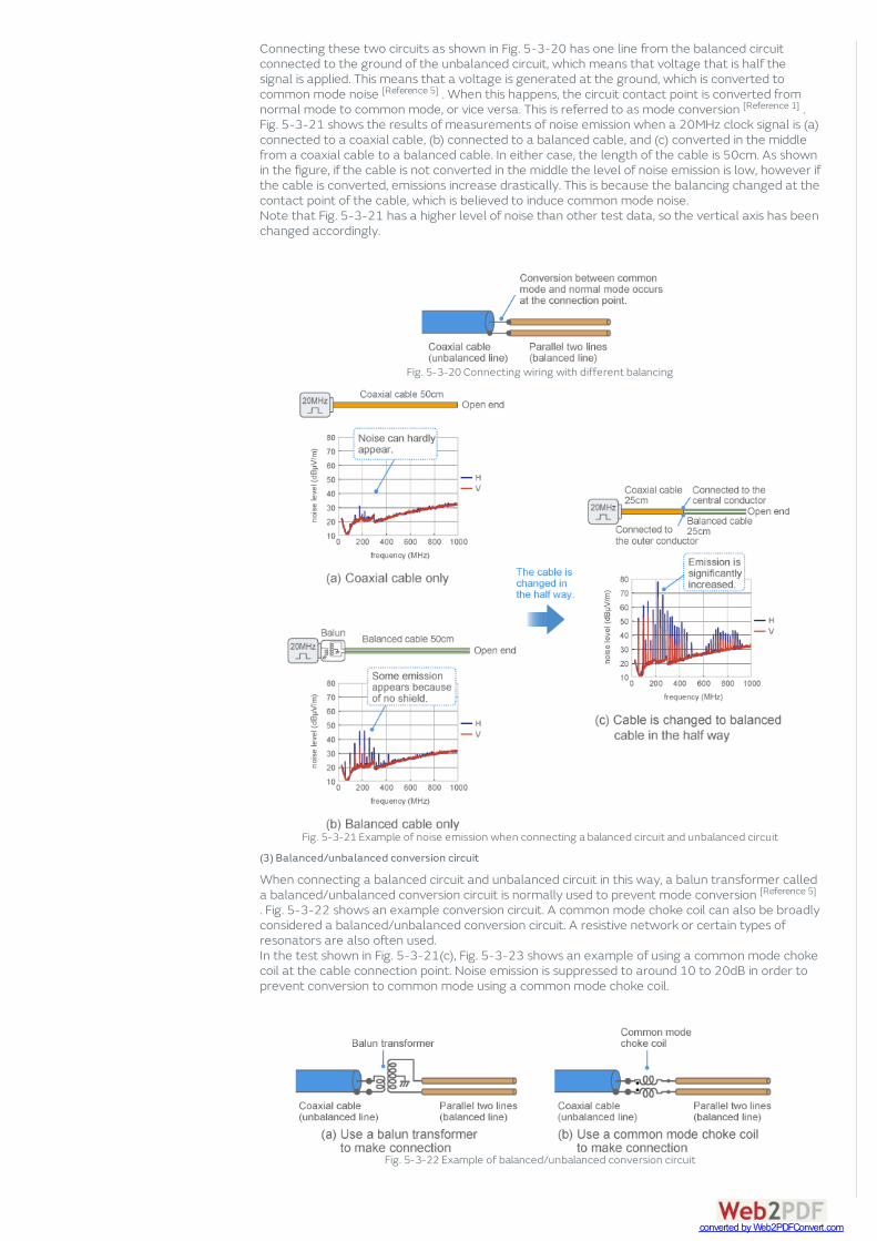
Connecting these two circuits as shown in Fig. 5-3-20 has one line from the balanced circuitconnected to the ground of the unbalanced circuit, which means that voltage that is half thesignal is applied. This means that a voltage is generated at the ground, which is converted tocommon mode noise . When this happens, the circuit contact point is converted fromnormal mode to common mode, or vice versa. This is referred to as mode conversion . Fig. 5-3-21 shows the results of measurements of noise emission when a 20MHz clock signal is (a)connected to a coaxial cable, (b) connected to a balanced cable, and (c) converted in the middlefrom a coaxial cable to a balanced cable. In either case, the length of the cable is 50cm. As shownin the figure, if the cable is not converted in the middle the level of noise emission is low, however ifthe cable is converted, emissions increase drastically. This is because the balancing changed at thecontact point of the cable, which is believed to induce common mode noise. Note that Fig. 5-3-21 has a higher level of noise than other test data, so the vertical axis has beenchanged accordingly.
Fig. 5-3-20 Connecting wiring with different balancing
Fig. 5-3-21 Example of noise emission when connecting a balanced circuit and unbalanced circuit
(3) Balanced/unbalanced conversion circuit
When connecting a balanced circuit and unbalanced circuit in this way, a balun transformer calleda balanced/unbalanced conversion circuit is normally used to prevent mode conversion . Fig. 5-3-22 shows an example conversion circuit. A common mode choke coil can also be broadlyconsidered a balanced/unbalanced conversion circuit. A resistive network or certain types ofresonators are also often used. In the test shown in Fig. 5-3-21(c), Fig. 5-3-23 shows an example of using a common mode chokecoil at the cable connection point. Noise emission is suppressed to around 10 to 20dB in order toprevent conversion to common mode using a common mode choke coil.
Fig. 5-3-22 Example of balanced/unbalanced conversion circuit
[Reference 5][Reference 1]
[Reference 5]
converted by Web2PDFConvert.com
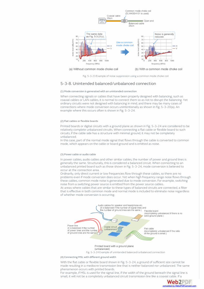
Fig. 5-3-23 Example of noise suppression using a common mode choke coil
5-3-8. Unintended balanced/unbalanced connection
(1) Mode conversion is generated with an unintended connection
When connecting signals or cables that have been properly designed with balancing, such ascoaxial cables or LAN cables, it is normal to connect them so as not to disrupt the balancing. Yetordinary circuits were not designed with balancing in mind, and there may be many cases ofconnections where mode conversion occurs unintentionally as shown in Fig. 5-3-20(a). Anexample where this occurs often is shown in Fig. 5-3-24.
(2) Flat cables or flexible boards
Printed boards or digital circuits with a ground plane as shown in Fig. 5-3-24 are considered to berelatively complete unbalanced circuits. When connecting a flat cable or flexible board to suchcircuits, if the cable side has a structure with minimal ground, it may not be completelyunbalanced. In this case, part of the normal mode signal that flows through the cable is converted to commonmode, which appears on the cable or board ground and is emitted as noise.
(3) Power cable or audio cable
In power cables, audio cables and other similar cables, the number of power and ground lines isgenerally the same. Structurally, this is considered a balanced circuit. When connecting to anunbalanced printed board such as those shown in Fig. 5-3-24, mode conversion is believed tooccur at the connection area. Ordinarily, only direct current or low frequencies flow through these cables, so there are noproblems even if mode conversion does occur. Yet when high frequency range noise flows throughthese cables, common mode noise is generated due to mode conversion. For example, switchingnoise from a switching power source is emitted from the power source cables. At areas where cables that are similar to these types of balanced circuits are connected, a filterthat is effective in both common mode and normal mode is included to eliminate noise regardlessof whether mode conversion is occurring.
Fig. 5-3-24 Example of unintended balanced/unbalanced connection
(4) Connecting MSL with different ground width
With the flat cable or flexible board shown in Fig. 5-3-24, a ground of sufficient size cannot bemade resulting in a mediocre transmission line that is neither balanced nor unbalanced. The samephenomenon occurs with printed boards. For example, if MSL is used for the signal line, if the width of the ground beneath the signal line issmall, it will not be a completely unbalanced circuit transmission line like a coaxial cable. If a
converted by Web2PDFConvert.com

normal mode current flows through such a line, the ground has a very small voltage. When connecting MSLs that have a different ground width together as shown in Fig. 5-3-25, thevoltage on the left and right MSL ground differs, which generates a voltage between the grounds. To suppress common mode noise, the ground width is suppressed so that the ground width of theleft and right MSL does not change. Alternatively, an EMI suppression filter can be used to removenoise elements flowing through the signal line in advance. The theory behind ground width suppression is explained with the current division ratio concept.Please refer to technical books for more details.
Fig. 5-3-25 Connecting MSL with different ground width
Top of page
“5-3 Common mode noise occurrence” - Key points
The mechanisms for generating common mode noise generated in ground includes
Current driving type modelCurrent driving type model
Voltage driving type modelVoltage driving type model
Common impedanceCommon impedance
Connection of balanced circuit and unbalanced circuitConnection of balanced circuit and unbalanced circuit
Care must be taken during the design of electronic devices so that these mechanisms are notincluded.
< Previous 1 22 3 Next >
[Reference 5]
Investor Relations About Murata Careers Contact us my Murata
ProductsProducts
Capacitors
Inductors
Noise Suppression Products /EMI Suppression Filters / ESDProtection Devices
Resistors
Thermistors
Sensors
ApplicationsApplications
Smarthome
Healthcare
Automotive
Mobile Communication
Network
Data Center
Lighting
About MurataAbout Murata
Company
Technology
Corporate SocialResponsibility
Newsroom
Investor Relations
Murata Robots
Procurement Guidelines
EU RoHS / REACHEU RoHS / REACHApproach for chemicalregulation for MurataProducts.
Find out more
converted by Web2PDFConvert.com

Timing Devices
Sound Components
Power Devices
Micro Mechatronics
RFID/NFC
Matching Devices
Balun
Coupler
Filters
Saw Based Components
Connectors
Isolators
Switch
Front-End Module
RF Modules
Wireless ConnectivityPlatforms
Ultra Low power Short RangeRF-IC
Substrates
Ionizers / Active OxygenModule (Ozonizers)
Industrial Equipment
White Goods
Personal Computers
Business Machine
AV
Security & Safety
Design ToolsDesign Tools
Web Software
Download
S-parameter
Netlist
Libraries
CAD
SupportSupport
Murata Locations
FAQs
Library
Health and SafetyCompliance
Avoiding CounterfeitProducts
Restriction of Weapons andMilitary End-Use
Copyright © Murata Manufacturing Co., Ltd. All Rights Reserved.Site Policy Privacy Site Help Sitemap
converted by Web2PDFConvert.com