Embed Size (px)
Citation preview
[Guide Subtitle] [optional]
UG440 (v2.0) May 4, 2009 [optional]
Xilinx Power Estimator User Guide
UG440 (v2.0) May 4, 2009
Xilinx Power Estimator User Guide www.xilinx.com UG440 (v2.0) May 4, 2009
Xilinx is disclosing this user guide, manual, release note, and/or specification (the "Documentation") to you solely for use in the development of designs to operate with Xilinx hardware devices. You may not reproduce, distribute, republish, download, display, post, or transmit the Documentation in any form or by any means including, but not limited to, electronic, mechanical, photocopying, recording, or otherwise, without the prior written consent of Xilinx. Xilinx expressly disclaims any liability arising out of your use of the Documentation. Xilinx reserves the right, at its sole discretion, to change the Documentation without notice at any time. Xilinx assumes no obligation to correct any errors contained in the Documentation, or to advise you of any corrections or updates. Xilinx expressly disclaims any liability in connection with technical support or assistance that may be provided to you in connection with the Information.
THE DOCUMENTATION IS DISCLOSED TO YOU “AS-IS” WITH NO WARRANTY OF ANY KIND. XILINX MAKES NO OTHER WARRANTIES, WHETHER EXPRESS, IMPLIED, OR STATUTORY, REGARDING THE DOCUMENTATION, INCLUDING ANY WARRANTIES OF MERCHANTABILITY, FITNESS FOR A PARTICULAR PURPOSE, OR NONINFRINGEMENT OF THIRD-PARTY RIGHTS. IN NO EVENT WILL XILINX BE LIABLE FOR ANY CONSEQUENTIAL, INDIRECT, EXEMPLARY, SPECIAL, OR INCIDENTAL DAMAGES, INCLUDING ANY LOSS OF DATA OR LOST PROFITS, ARISING FROM YOUR USE OF THE DOCUMENTATION.
© 2007–2009 Xilinx, Inc. XILINX, the Xilinx logo, Virtex, Spartan, ISE, and other designated brands included herein are trademarks of Xilinx in the United States and other countries. All other trademarks are the property of their respective owners.
UG440 (v2.0) May 4, 2009 www.xilinx.com Xilinx Power Estimator User Guide
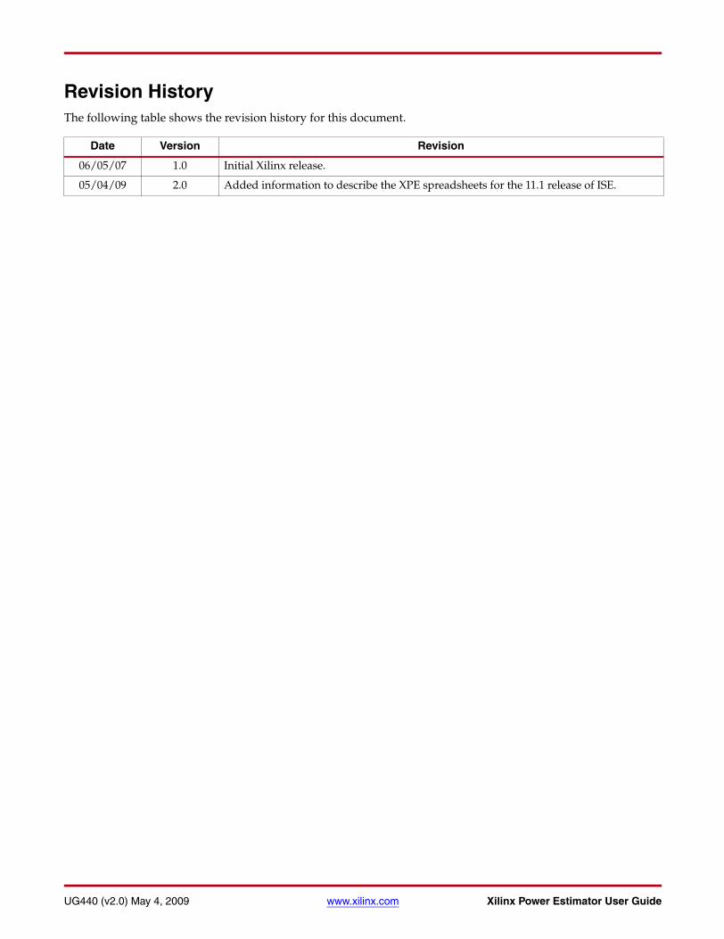
Revision HistoryThe following table shows the revision history for this document.
Date Version Revision
06/05/07 1.0 Initial Xilinx release.
05/04/09 2.0 Added information to describe the XPE spreadsheets for the 11.1 release of ISE.
Xilinx Power Estimator User Guide www.xilinx.com 5UG440 (v2.0) May 4, 2009
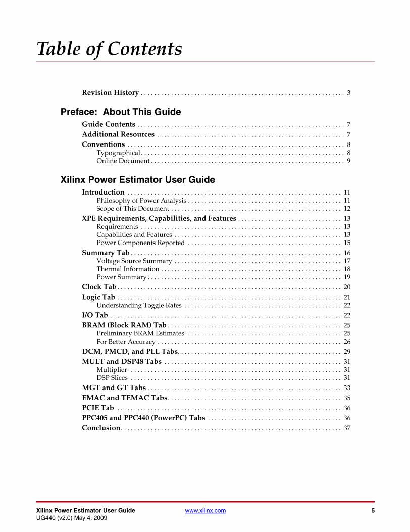
Revision History . . . . . . . . . . . . . . . . . . . . . . . . . . . . . . . . . . . . . . . . . . . . . . . . . . . . . . . . . . . . . 3
Preface: About This GuideGuide Contents . . . . . . . . . . . . . . . . . . . . . . . . . . . . . . . . . . . . . . . . . . . . . . . . . . . . . . . . . . . . . . 7Additional Resources . . . . . . . . . . . . . . . . . . . . . . . . . . . . . . . . . . . . . . . . . . . . . . . . . . . . . . . . 7Conventions . . . . . . . . . . . . . . . . . . . . . . . . . . . . . . . . . . . . . . . . . . . . . . . . . . . . . . . . . . . . . . . . . 8
Typographical . . . . . . . . . . . . . . . . . . . . . . . . . . . . . . . . . . . . . . . . . . . . . . . . . . . . . . . . . . . . . 8Online Document . . . . . . . . . . . . . . . . . . . . . . . . . . . . . . . . . . . . . . . . . . . . . . . . . . . . . . . . . . 9
Xilinx Power Estimator User GuideIntroduction . . . . . . . . . . . . . . . . . . . . . . . . . . . . . . . . . . . . . . . . . . . . . . . . . . . . . . . . . . . . . . . . 11
Philosophy of Power Analysis . . . . . . . . . . . . . . . . . . . . . . . . . . . . . . . . . . . . . . . . . . . . . . 11Scope of This Document . . . . . . . . . . . . . . . . . . . . . . . . . . . . . . . . . . . . . . . . . . . . . . . . . . . 12
XPE Requirements, Capabilities, and Features . . . . . . . . . . . . . . . . . . . . . . . . . . . . . . . 13Requirements . . . . . . . . . . . . . . . . . . . . . . . . . . . . . . . . . . . . . . . . . . . . . . . . . . . . . . . . . . . . 13Capabilities and Features . . . . . . . . . . . . . . . . . . . . . . . . . . . . . . . . . . . . . . . . . . . . . . . . . . 13Power Components Reported . . . . . . . . . . . . . . . . . . . . . . . . . . . . . . . . . . . . . . . . . . . . . . 15
Summary Tab . . . . . . . . . . . . . . . . . . . . . . . . . . . . . . . . . . . . . . . . . . . . . . . . . . . . . . . . . . . . . . . 16Voltage Source Summary . . . . . . . . . . . . . . . . . . . . . . . . . . . . . . . . . . . . . . . . . . . . . . . . . . 17Thermal Information . . . . . . . . . . . . . . . . . . . . . . . . . . . . . . . . . . . . . . . . . . . . . . . . . . . . . . 18Power Summary . . . . . . . . . . . . . . . . . . . . . . . . . . . . . . . . . . . . . . . . . . . . . . . . . . . . . . . . . . 19
Clock Tab . . . . . . . . . . . . . . . . . . . . . . . . . . . . . . . . . . . . . . . . . . . . . . . . . . . . . . . . . . . . . . . . . . . 20Logic Tab . . . . . . . . . . . . . . . . . . . . . . . . . . . . . . . . . . . . . . . . . . . . . . . . . . . . . . . . . . . . . . . . . . . 21
Understanding Toggle Rates . . . . . . . . . . . . . . . . . . . . . . . . . . . . . . . . . . . . . . . . . . . . . . . 22I/O Tab . . . . . . . . . . . . . . . . . . . . . . . . . . . . . . . . . . . . . . . . . . . . . . . . . . . . . . . . . . . . . . . . . . . . . 22BRAM (Block RAM) Tab . . . . . . . . . . . . . . . . . . . . . . . . . . . . . . . . . . . . . . . . . . . . . . . . . . . . 25
Preliminary BRAM Estimates . . . . . . . . . . . . . . . . . . . . . . . . . . . . . . . . . . . . . . . . . . . . . . 25For Better Accuracy . . . . . . . . . . . . . . . . . . . . . . . . . . . . . . . . . . . . . . . . . . . . . . . . . . . . . . . 26
DCM, PMCD, and PLL Tabs. . . . . . . . . . . . . . . . . . . . . . . . . . . . . . . . . . . . . . . . . . . . . . . . . 29MULT and DSP48 Tabs . . . . . . . . . . . . . . . . . . . . . . . . . . . . . . . . . . . . . . . . . . . . . . . . . . . . . 31
Multiplier . . . . . . . . . . . . . . . . . . . . . . . . . . . . . . . . . . . . . . . . . . . . . . . . . . . . . . . . . . . . . . . 31DSP Slices . . . . . . . . . . . . . . . . . . . . . . . . . . . . . . . . . . . . . . . . . . . . . . . . . . . . . . . . . . . . . . . 31
MGT and GT Tabs . . . . . . . . . . . . . . . . . . . . . . . . . . . . . . . . . . . . . . . . . . . . . . . . . . . . . . . . . . 33EMAC and TEMAC Tabs. . . . . . . . . . . . . . . . . . . . . . . . . . . . . . . . . . . . . . . . . . . . . . . . . . . . 35PCIE Tab . . . . . . . . . . . . . . . . . . . . . . . . . . . . . . . . . . . . . . . . . . . . . . . . . . . . . . . . . . . . . . . . . . . 36PPC405 and PPC440 (PowerPC) Tabs . . . . . . . . . . . . . . . . . . . . . . . . . . . . . . . . . . . . . . . . 36Conclusion. . . . . . . . . . . . . . . . . . . . . . . . . . . . . . . . . . . . . . . . . . . . . . . . . . . . . . . . . . . . . . . . . . 37
Table of Contents
Xilinx Power Estimator User Guide www.xilinx.com 7UG440 (v2.0) May 4, 2009
Preface
About This Guide
This User Guide describes the Xilinx Power Estimator (XPE), a power estimation tool used in the predesign and preimplementation phases of a design to be implemented in a Xilinx FPGA. XPE works with Microsoft Excel.
XPE currently supports all Spartan™-3 Generation FPGAs (Spartan-3, Spartan-3A, Spartan-3AN, and Spartan-3A DSP), Virtex™-4 FPGAs, and Virtex-5 FPGAs. Predesign power estimation support for earlier Xilinx FPGA devices is done through the Web Power Tool (WPT), which works with web browsers and is available from the Xilinx website.
For additional details about XPE, see the Power Solutions webpage on the Xilinx website.
Guide ContentsThis manual contains the following chapter:
• “Xilinx Power Estimator User Guide”
Additional ResourcesTo find additional documentation, see the Xilinx website at:
http://www.xilinx.com/literature
To search the Answer Database of silicon, software, and IP questions and answers, or to create a technical support WebCase, see the Xilinx website at:
http://www.xilinx.com/support
To download the XPE spreadsheets, see the Power Solutions webpage on the Xilinx website at:
http://www.xilinx.com/power
The following are especially pertinent to the subject of this User Guide.
• WP353: Seven Steps to an Accurate Worst-Case Power Analysis Using Xilinx Power Estimator (XPE)
• Test Boards for Area Array Surface Mount Package Thermal Measurements
• UG331: Spartan-3 Generation FPGA User Guide
• UG070: Virtex-4 FPGA User Guide
• UG190: Virtex-5 FPGA User Guide
• UG112: Device Package User Guide
• User Guides for dedicated blocks within the FPGAs (for example, DSP and MGT blocks) are referenced in the sections describing power estimation for these blocks.
8 www.xilinx.com Xilinx Power Estimator User GuideUG440 (v2.0) May 4, 2009
Preface: About This Guide
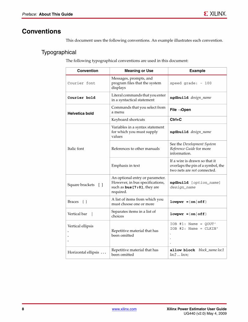
ConventionsThis document uses the following conventions. An example illustrates each convention.
TypographicalThe following typographical conventions are used in this document:
Convention Meaning or Use Example
Courier fontMessages, prompts, and program files that the system displays
speed grade: - 100
Courier boldLiteral commands that you enter in a syntactical statement
ngdbuild design_name
Helvetica bold
Commands that you select from a menu
File →Open
Keyboard shortcuts Ctrl+C
Italic font
Variables in a syntax statement for which you must supply values
ngdbuild design_name
References to other manualsSee the Development System Reference Guide for more information.
Emphasis in textIf a wire is drawn so that it overlaps the pin of a symbol, the two nets are not connected.
Square brackets [ ]
An optional entry or parameter. However, in bus specifications, such as bus[7:0], they are required.
ngdbuild [option_name] design_name
Braces { }A list of items from which you must choose one or more
lowpwr ={on|off}
Vertical bar |Separates items in a list of choices
lowpwr ={on|off}
Vertical ellipsis...
Repetitive material that has been omitted
IOB #1: Name = QOUT’ IOB #2: Name = CLKIN’...
Horizontal ellipsis . . .Repetitive material that has been omitted
allow block block_name loc1 loc2 ... locn;
Xilinx Power Estimator User Guide www.xilinx.com 9UG440 (v2.0) May 4, 2009
Conventions
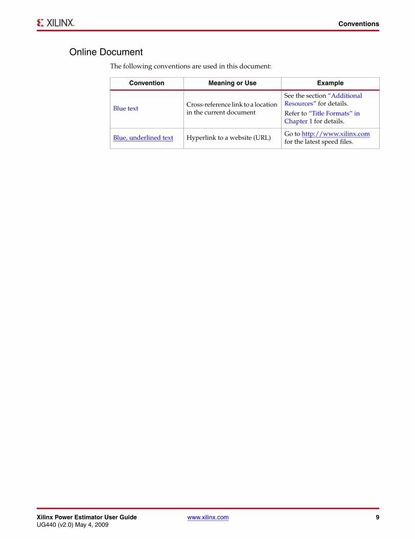
Online DocumentThe following conventions are used in this document:
Convention Meaning or Use Example
Blue textCross-reference link to a location in the current document
See the section “Additional Resources” for details.
Refer to “Title Formats” in Chapter 1 for details.
Blue, underlined text Hyperlink to a website (URL)Go to http://www.xilinx.com for the latest speed files.
10 www.xilinx.com Xilinx Power Estimator User GuideUG440 (v2.0) May 4, 2009
Preface: About This Guide
Xilinx Power Estimator User Guide www.xilinx.com 11UG440 (v2.0) May 4, 2009
Xilinx Power Estimator User Guide
IntroductionXilinx Power Estimator (XPE) is a power estimation tool intended to be used for the predesign/preimplementation phase. XPE works with Microsoft Excel.
XPE currently supports the Spartan™-3 Generation FPGAs, Virtex™-4, and Virtex-5 devices.
XPE considers the design resource usage, toggle rates, I/O loading, and many other factors in the estimation process. The formulas used for calculations in the program are based on intended behavior of various digital circuits. The characteristic data is based on measurements, simulation, and/or extrapolation.
XPE is a preimplementation tool for use in the early stages of a design. After implementation, the XPower Analyzer (XPA) tool (available in the ISE® Design Suite software) can be used for more accurate estimates and power analysis, since XPower Analyzer utilizes the logic and routing resources of the actual design.
XPE is primarily a spreadsheet, so all MS Excel-based functionality is fully retained in the writable or unprotected sections of the spreadsheet. XPE has additional functionality oriented to ease of use. The drop-down menus and the comment-enabled cells are useful features that are helpful to the user.
Philosophy of Power AnalysisPower analysis for programmable devices is motivated by three main aspects:
• Power supply sizing or selection
• Thermal management
• Identifying the candidate functional blocks for power reduction
Xilinx power estimation is analogous to static timing analysis. Power estimation and analysis tools can be used to report worst-case and typical power margins. The accuracy of XPE is dependent on two primary components:
• The inputs you enter into XPE to model designs
• The characterization data integrated into the tool that stems from device characterization
For realistic estimates specific to your application, enter realistic voltage and temperature conditions. Modeling a certain aspect of the design over-conservatively or without sufficient knowledge of the design can result in unrealistic estimates. Some techniques to drive the XPE to provide worst-case estimates or typical estimates are discussed in this document.
12 www.xilinx.com Xilinx Power Estimator User GuideUG440 (v2.0) May 4, 2009
Introduction
The following document provides additional information useful for accurate power analysis with XPE:
WP353: Seven Steps to an Accurate Worst-Case Power Analysis Using Xilinx Power Estimator (XPE)
The accuracy of the characterization data existing in the tool is reflected by accuracy designations in the Release tab of XPE. For most FPGAs, the accuracy designation is also displayed in the Data field of the Power Summary section of the Summary tab. The accuracy designations are Advanced, Preliminary, and Production.
Advanced
The data integrated into XPE with this designation is based primarily on measurements and characterization data made on early production devices. A set of widely used device resources are included in the characterization. Characterization data is limited to these few blocks. This data is typically available within a year of product launch. Although the data with this designation is considered relatively stable and conservative, some under-reporting or over-reporting might occur. Advanced data accuracy is considerably lower than the Preliminary and Production data.
Preliminary
The data integrated into XPE with this designation is based on complete early production silicon. Almost all the blocks in the device fabric are characterized. Data for most of the dedicated blocks like TEMAC and PCIe block are also characterized and integrated into the XPE. The probability of accurate power reporting is improved as compared to Advanced data.
Production
The data integrated into XPE with this designation is released after enough production silicon of a particular device family member has been characterized to provide full power correlation over numerous production lots. Characterization data for all blocks in the device fabric is included.
Scope of This DocumentThe purpose of this document is to describe how to use XPE to arrive at realistic estimates for real-life designs. Simple example circuits are included to illustrate the use of the tool. Examples include 16-bit counters, common block RAM configurations, and clock trees. This document also shows:
• Tool features that make design data entry, capture, and storage convenient, and
• A detailed description of the various spreadsheet tabs that are a part of the tool, their purpose, and usage.
This document focuses on how to use XPE to calculate estimated power consumption for supported devices.
White Paper WP353: Seven Steps to an Accurate Worst-Case Power Analysis Using Xilinx Power Estimator (XPE) also provides supplementary information useful for power analysis with XPE.
Xilinx Power Estimator User Guide www.xilinx.com 13UG440 (v2.0) May 4, 2009
XPE Requirements, Capabilities, and Features
XPE Requirements, Capabilities, and Features
RequirementsXPE requires a licensed version of Microsoft Excel 2003 or later to be installed. XPE can be accessed on the Xilinx website at http://www.xilinx.com/power. There are separate downloadable XPE spreadsheets for each of these devices:
• Virtex-4
• Virtex-5
• Spartan-3
• Spartan-3E
• Spartan-3A (also supports Spartan-3AN)
• Spartan-3A DSP
XPE uses several macros built into the XPE spreadsheet. By default, the Microsoft Excel 2003 macro security level is set to High, which automatically disables macros. To change the macro security level, follow these steps in Microsoft Excel 2003:
1. On the Tools menu, point to Macro and click Security.
2. In the Security dialog box, click the Security Level tab.
3. Select Medium, then click OK.
4. Open or, if already open, reopen the XPE spreadsheet.
5. When prompted whether to enable or disable macros, click Enable Macros.
Capabilities and FeaturesPower estimation for programmable devices like FPGAs is a complex process. To produce accurate estimates, the power estimation process requires accurate input values, such as resource utilization, clock rates, and toggle rates. To use this tool to its minimum capability with reasonable accuracy, you need the following:
• A target device-package combination
• A good estimate of resources you expect to use in the design (for example, flip-flops, look-up tables, I/Os, block RAMS, DCMs, etc.)
• The clock frequency or frequencies for the design
• An estimate of the data toggle rates for the design
This minimum data is necessary but not sufficient to provide accurate estimates that aid an optimal choice of power supplies, regulators, and optional thermal solutions.
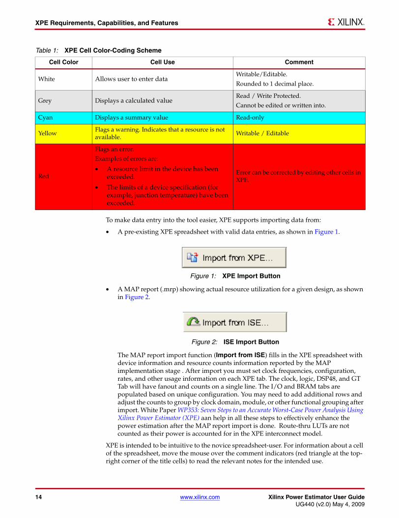
A description of the spreadsheet’s color-coding scheme is provided in Table 1.
14 www.xilinx.com Xilinx Power Estimator User GuideUG440 (v2.0) May 4, 2009
XPE Requirements, Capabilities, and Features
To make data entry into the tool easier, XPE supports importing data from:
• A pre-existing XPE spreadsheet with valid data entries, as shown in Figure 1.X-Ref Target - Figure 1
• A MAP report (.mrp) showing actual resource utilization for a given design, as shown in Figure 2.
X-Ref Target - Figure 2
The MAP report import function (Import from ISE) fills in the XPE spreadsheet with device information and resource counts information reported by the MAP implementation stage . After import you must set clock frequencies, configuration, rates, and other usage information on each XPE tab. The clock, logic, DSP48, and GT Tab will have fanout and counts on a single line. The I/O and BRAM tabs are populated based on unique configuration. You may need to add additional rows and adjust the counts to group by clock domain, module, or other functional grouping after import. White Paper WP353: Seven Steps to an Accurate Worst-Case Power Analysis Using Xilinx Power Estimator (XPE) aan help in all these steps to effectively enhance the power estimation after the MAP report import is done. Route-thru LUTs are not counted as their power is accounted for in the XPE interconnect model.
XPE is intended to be intuitive to the novice spreadsheet-user. For information about a cell of the spreadsheet, move the mouse over the comment indicators (red triangle at the top-right corner of the title cells) to read the relevant notes for the intended use.
Table 1: XPE Cell Color-Coding Scheme
Cell Color Cell Use Comment
White Allows user to enter dataWritable/Editable.
Rounded to 1 decimal place.
Grey Displays a calculated valueRead / Write Protected.
Cannot be edited or written into.
Cyan Displays a summary value Read-only
YellowFlags a warning. Indicates that a resource is not available.
Writable / Editable
Red
Flags an error.
Examples of errors are:
• A resource limit in the device has been exceeded.
• The limits of a device specification (for example, junction temperature) have been exceeded.
Error can be corrected by editing other cells in XPE.
Figure 1: XPE Import Button
Figure 2: ISE Import Button
Xilinx Power Estimator User Guide www.xilinx.com 15UG440 (v2.0) May 4, 2009
XPE Requirements, Capabilities, and Features
Power Components ReportedAs with any CMOS-based SRAM device, the power consumption reported by the tool for FPGAs has two appreciable components:
• Static power (referred to as quiescent power in XPE)
• Dynamic power
The device quiescent power is automatically determined depending on the device selected. No input into XPE is required. The estimates represent power drawn by the device when there is no switching activity. By choosing the Maximum or Typical values for Process, worst-case or nominal power can be estimated.
Both the reported static and dynamic power estimates are modeled to account for temperature and voltage sensitivity. Ambient temperature and regulated voltage on the system can be keyed into the appropriate cells provided for the purpose.
16 www.xilinx.com Xilinx Power Estimator User GuideUG440 (v2.0) May 4, 2009
Summary Tab
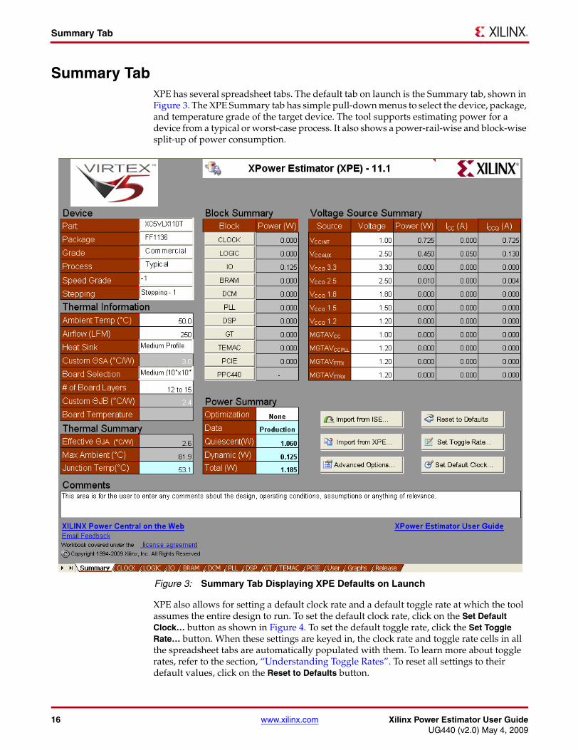
Summary TabXPE has several spreadsheet tabs. The default tab on launch is the Summary tab, shown in Figure 3. The XPE Summary tab has simple pull-down menus to select the device, package, and temperature grade of the target device. The tool supports estimating power for a device from a typical or worst-case process. It also shows a power-rail-wise and block-wise split-up of power consumption.X-Ref Target - Figure 3
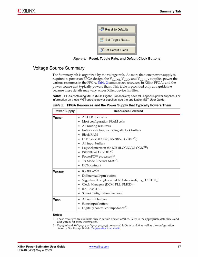
XPE also allows for setting a default clock rate and a default toggle rate at which the tool assumes the entire design to run. To set the default clock rate, click on the Set Default Clock… button as shown in Figure 4. To set the default toggle rate, click the Set Toggle Rate… button. When these settings are keyed in, the clock rate and toggle rate cells in all the spreadsheet tabs are automatically populated with them. To learn more about toggle rates, refer to the section, “Understanding Toggle Rates”. To reset all settings to their default values, click on the Reset to Defaults button.
Figure 3: Summary Tab Displaying XPE Defaults on Launch
Xilinx Power Estimator User Guide www.xilinx.com 17UG440 (v2.0) May 4, 2009
Summary Tab
X-Ref Target - Figure 4
Voltage Source SummaryThe Summary tab is organized by the voltage rails. As more than one power supply is required to power an FPGA design, the VCCINT, VCCO, and VCCAUX supplies power the various resources in the FPGA. Table 2 summarizes resources in Xilinx FPGAs and the power source that typically powers them. This table is provided only as a guideline because these details may vary across Xilinx device families.
Note: FPGAs containing MGTs (Multi Gigabit Transceivers) have MGT-specific power supplies. For information on these MGT-specific power supplies, see the applicable MGT User Guide.
Figure 4: Reset, Toggle Rate, and Default Clock Buttons
Table 2: FPGA Resources and the Power Supply that Typically Powers Them
Power Supply Resources Powered
VCCINT • All CLB resources• Most configuration SRAM cells • All routing resources• Entire clock tree, including all clock buffers• Block RAM• DSP blocks (DSP48, DSP48A, DSP48E(1))• All input buffers• Logic elements in the IOB (ILOGIC/OLOGIC(1))• ISERDES/OSERDES(1)
• PowerPC™ processor(1)
• Tri-Mode Ethernet MAC(1)
• DCM (minor)
VCCAUX • IODELAY(1)
• Differential Input buffers• VREF-based, single-ended I/O standards, e.g., HSTL18_I• Clock Managers (DCM, PLL, PMCD)(1)
• IDELAYCTRL• Some Configuration memory
VCCO • All output buffers • Some input buffers• Digitally controlled impedance(2)
Notes: 1. These resources are available only in certain device families. Refer to the appropriate data sheets and
user guides for more information.2. VCCO in bank 0 (VCCO_0 or VCCO_CONFIG) powers all I/Os in bank 0 as well as the configuration
circuitry. See the applicable Configuration User Guide.
18 www.xilinx.com Xilinx Power Estimator User GuideUG440 (v2.0) May 4, 2009
Summary Tab
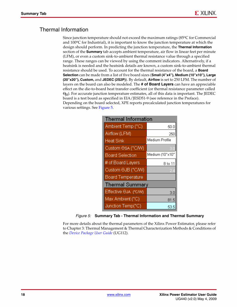
Thermal InformationSince junction temperature should not exceed the maximum ratings (85oC for Commercial and 100oC for Industrial), it is important to know the junction temperature at which the design should perform. In predicting the junction temperature, the Thermal Information section of the Summary tab accepts ambient temperature, air flow in linear feet per minute (LFM), or even a custom sink-to-ambient thermal resistance value through a specified range. These ranges can be viewed by using the comment indicators. Alternatively, if a heatsink is needed and the heatsink details are known, a custom sink-to-ambient thermal resistance should be used. To account for the thermal resistance of the board, a Board Selection can be made from a list of five board sizes (Small (4”x4”), Medium (10”x10”), Large (20”x20”), Custom, and JEDEC (2S2P)). By default, Airflow is set to 250 LFM. The number of layers on the board can also be modeled. The # of Board Layers can have an appreciable effect on the die-to-board heat transfer coefficient (or thermal resistance parameter called ΘJB). For accurate junction temperature estimates, all of this data is important. The JEDEC board is a test board as specified in EIA/JESD51-9 (see reference in the Preface). Depending on the board selected, XPE reports precalculated junction temperatures for various settings. See Figure 5.X-Ref Target - Figure 5
For more details about the thermal parameters of the Xilinx Power Estimator, please refer to Chapter 3: Thermal Management & Thermal Characterization Methods & Conditions of the Device Package User Guide (UG112).
Figure 5: Summary Tab - Thermal Information and Thermal Summary
Xilinx Power Estimator User Guide www.xilinx.com 19UG440 (v2.0) May 4, 2009
Summary Tab
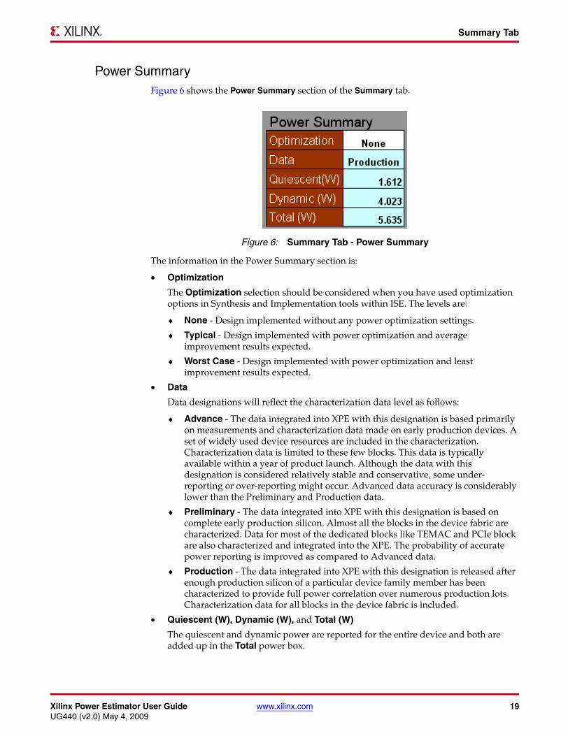
Power SummaryFigure 6 shows the Power Summary section of the Summary tab.X-Ref Target - Figure 6
The information in the Power Summary section is:
• Optimization
The Optimization selection should be considered when you have used optimization options in Synthesis and Implementation tools within ISE. The levels are:
♦ None - Design implemented without any power optimization settings.
♦ Typical - Design implemented with power optimization and average improvement results expected.
♦ Worst Case - Design implemented with power optimization and least improvement results expected.
• Data
Data designations will reflect the characterization data level as follows:
♦ Advance - The data integrated into XPE with this designation is based primarily on measurements and characterization data made on early production devices. A set of widely used device resources are included in the characterization. Characterization data is limited to these few blocks. This data is typically available within a year of product launch. Although the data with this designation is considered relatively stable and conservative, some under-reporting or over-reporting might occur. Advanced data accuracy is considerably lower than the Preliminary and Production data.
♦ Preliminary - The data integrated into XPE with this designation is based on complete early production silicon. Almost all the blocks in the device fabric are characterized. Data for most of the dedicated blocks like TEMAC and PCIe block are also characterized and integrated into the XPE. The probability of accurate power reporting is improved as compared to Advanced data.
♦ Production - The data integrated into XPE with this designation is released after enough production silicon of a particular device family member has been characterized to provide full power correlation over numerous production lots. Characterization data for all blocks in the device fabric is included.
• Quiescent (W), Dynamic (W), and Total (W)
The quiescent and dynamic power are reported for the entire device and both are added up in the Total power box.
Figure 6: Summary Tab - Power Summary
20 www.xilinx.com Xilinx Power Estimator User GuideUG440 (v2.0) May 4, 2009
Clock Tab
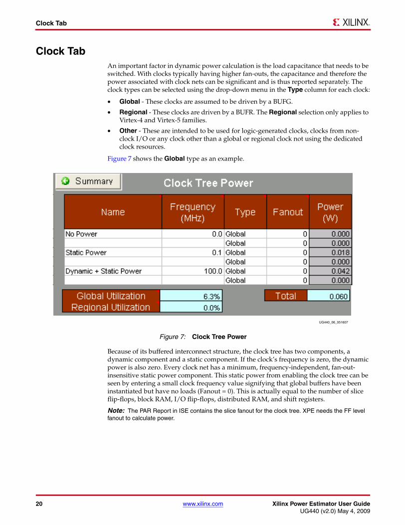
Clock TabAn important factor in dynamic power calculation is the load capacitance that needs to be switched. With clocks typically having higher fan-outs, the capacitance and therefore the power associated with clock nets can be significant and is thus reported separately. The clock types can be selected using the drop-down menu in the Type column for each clock:
• Global - These clocks are assumed to be driven by a BUFG.
• Regional - These clocks are driven by a BUFR. The Regional selection only applies to Virtex-4 and Virtex-5 families.
• Other - These are intended to be used for logic-generated clocks, clocks from non-clock I/O or any clock other than a global or regional clock not using the dedicated clock resources.
Figure 7 shows the Global type as an example.X-Ref Target - Figure 7
Because of its buffered interconnect structure, the clock tree has two components, a dynamic component and a static component. If the clock’s frequency is zero, the dynamic power is also zero. Every clock net has a minimum, frequency-independent, fan-out-insensitive static power component. This static power from enabling the clock tree can be seen by entering a small clock frequency value signifying that global buffers have been instantiated but have no loads (Fanout = 0). This is actually equal to the number of slice flip-flops, block RAM, I/O flip-flops, distributed RAM, and shift registers.
Note: The PAR Report in ISE contains the slice fanout for the clock tree. XPE needs the FF level fanout to calculate power.
Figure 7: Clock Tree Power
UG440_06_051607
Xilinx Power Estimator User Guide www.xilinx.com 21UG440 (v2.0) May 4, 2009
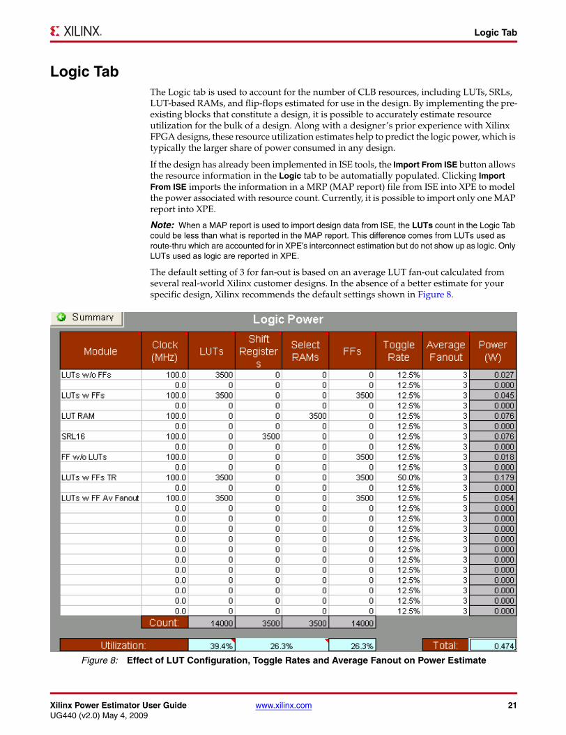
Logic Tab
Logic TabThe Logic tab is used to account for the number of CLB resources, including LUTs, SRLs, LUT-based RAMs, and flip-flops estimated for use in the design. By implementing the pre-existing blocks that constitute a design, it is possible to accurately estimate resource utilization for the bulk of a design. Along with a designer’s prior experience with Xilinx FPGA designs, these resource utilization estimates help to predict the logic power, which is typically the larger share of power consumed in any design.
If the design has already been implemented in ISE tools, the Import From ISE button allows the resource information in the Logic tab to be automatially populated. Clicking Import From ISE imports the information in a MRP (MAP report) file from ISE into XPE to model the power associated with resource count. Currently, it is possible to import only one MAP report into XPE.
Note: When a MAP report is used to import design data from ISE, the LUTs count in the Logic Tab could be less than what is reported in the MAP report. This difference comes from LUTs used as route-thru which are accounted for in XPE’s interconnect estimation but do not show up as logic. Only LUTs used as logic are reported in XPE.
The default setting of 3 for fan-out is based on an average LUT fan-out calculated from several real-world Xilinx customer designs. In the absence of a better estimate for your specific design, Xilinx recommends the default settings shown in Figure 8.X-Ref Target - Figure 8
Figure 8: Effect of LUT Configuration, Toggle Rates and Average Fanout on Power Estimate
22 www.xilinx.com Xilinx Power Estimator User GuideUG440 (v2.0) May 4, 2009
I/O Tab
Understanding Toggle RatesA less intuitive detail is modeling the toggle rates for the various sections of the design or estimating an average toggle rate for the entire design. Toggle rate reflects how often an output changes relative to a given clock input and can be modeled as a percentage between 0–100%. The max data toggle rate of 100% means that if the clock frequency is 100 MHz, a data toggle rate of 100% equates to a data frequency of 50 MHz. This convention stems from an assumption that a net with a 100% toggle rate toggles every rising (or falling) edge of a clock whose frequency is specified. So, this means that the LSB of a 16-bit counter toggles every clock cycle and the MSB toggles every 32,768th clock cycle. The default toggle rate picked by XPE is 12.5%, which accounts for the average toggle rate of a 16-bit counter.
For nonperiodic or event-driven state machine designs, toggle rates cannot be easily predicted. An effective method of estimating average toggle rates for a given design is to segregate the different sections of the design based on their functionality and estimate the toggle rates for each of the sub-blocks. An average toggle rate can then be arrived at by calculating the average for the entire design. Most logic-intensive designs work at around 12.5% average toggle rate, which is the default toggle rate setting in XPE. For a worst- case estimate, a toggle rate of 20% can be used. Average toggle rates greater than 20% are not very common. Arithmetic-intensive modules of a design seem to take toggle rates of up to 50%, which is representative of the absolute worst case. An example of this would be a Multiply-Accumulate operation. It is also common to model toggle rate for random input data at 50%. Data toggle rate should be scaled by the Clock Enable rates. If data toggle rate is modeled at 50% but the slice logic is clock-enabled 50 percent of the time, the resulting toggle rate should be 25%. To appreciate what 100% toggle rate means, think of a constantly enabled toggle flip-flop (TFF) whose data input is tied High. The T-output of this flip-flop toggles every clock edge. Very few designs could possibly have an average toggle rate that high (100%).
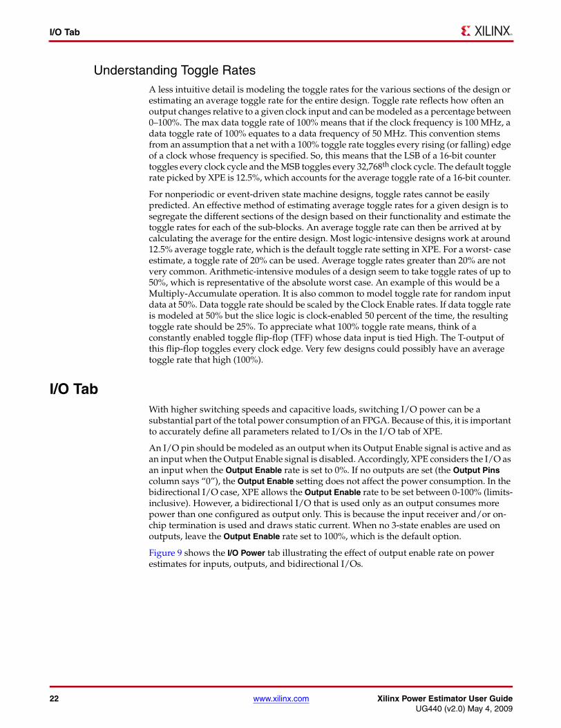
I/O TabWith higher switching speeds and capacitive loads, switching I/O power can be a substantial part of the total power consumption of an FPGA. Because of this, it is important to accurately define all parameters related to I/Os in the I/O tab of XPE.
An I/O pin should be modeled as an output when its Output Enable signal is active and as an input when the Output Enable signal is disabled. Accordingly, XPE considers the I/O as an input when the Output Enable rate is set to 0%. If no outputs are set (the Output Pins column says “0”), the Output Enable setting does not affect the power consumption. In the bidirectional I/O case, XPE allows the Output Enable rate to be set between 0-100% (limits-inclusive). However, a bidirectional I/O that is used only as an output consumes more power than one configured as output only. This is because the input receiver and/or on-chip termination is used and draws static current. When no 3-state enables are used on outputs, leave the Output Enable rate set to 100%, which is the default option.
Figure 9 shows the I/O Power tab illustrating the effect of output enable rate on power estimates for inputs, outputs, and bidirectional I/Os.
Xilinx Power Estimator User Guide www.xilinx.com 23UG440 (v2.0) May 4, 2009
I/O Tab
X-Ref Target - Figure 9
Different I/O standards have different termination requirements. A significant proportion of I/O power can be accounted for through I2R loss in these terminations. I/O standards such as HSTL and SSTL require terminations to VTT which can be an independent or derived power supply from VCCO. The VCCO supply current reported by XPE assumes that these terminations are as required by the I/O standard and that VTT is derived fromVCCO. Refer to the applicable FPGA User Guide (listed in “Additional Resources”) for specific terminations recommended and used by XPE for calculations.
Some I/O standards (especially those that involve open drain drivers) can contribute no appreciable power draw from the VCCO supply that powers the driver while drawing power from the receiver’s VCCO. These drivers can potentially contribute only to the I2R power loss rather than drawing any current from the driver’s VCCO rail. As these I/Os contribute purely to the junction temperature estimate, XPE additionally reports VCCO on-chip thermal power which is only used in predicting junction temperature for the design.
Figure 9: I/O Tab - Effect of Output Enable Rate on Power Estimates for Inputs, Outputs, and Bidirectional I/Os
24 www.xilinx.com Xilinx Power Estimator User GuideUG440 (v2.0) May 4, 2009
I/O Tab
XPE calculates the portion of VCCO dissipated on-chip for thermal considerations. It also calculates the required supply current including current drawn into off-chip termination resistors.
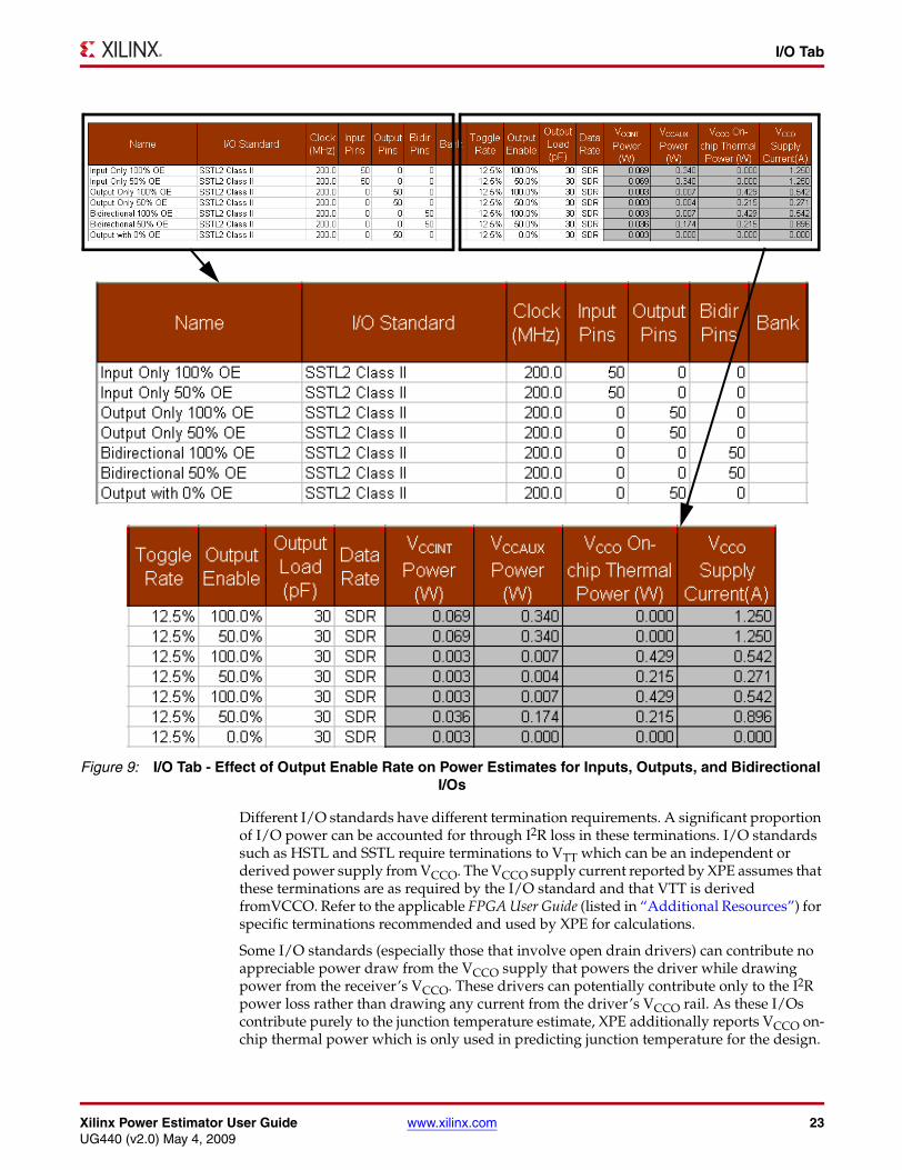
Toggle rates for I/Os are typically in the range of 10–15%. The default setting is 12.5%. The most conservative or worst-case I/O power estimates can be reasonably modeled using toggle rates of 30–35%. For differential I/O standards such as LVDS, DIFF_HSTL, etc., enter the number of pairs of differential pins. For example, to model 8 LVDS input pairs (16 pins), enter 8 into the corresponding cell in Input Pins column. Figure 10 shows a portion of an I/O Tab showing a differential pair count entry.X-Ref Target - Figure 10
Figure 10: I/O Power Tab - Differential Pair Count Entry
Xilinx Power Estimator User Guide www.xilinx.com 25UG440 (v2.0) May 4, 2009
BRAM (Block RAM) Tab
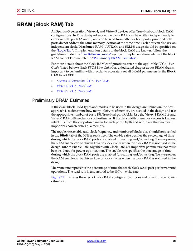
BRAM (Block RAM) TabAll Spartan-3 generation, Virtex-4, and Virtex-5 devices offer True dual-port block RAM configurations. In True dual-port mode, the block RAM can be written independently to either or both ports (A and B) and can be read from either or both ports, provided both ports do not address the same memory location at the same time. Each port can also use an independent clock. Distributed RAM (LUTRAM and SRL16) usage should be specified on the “Logic Tab”. If implementation details of the block RAM are known, follow the guidelines under the “For Better Accuracy” section. If implementation details of the block RAM are not known, refer to “Preliminary BRAM Estimates”.
For more details about the block RAM configurations, refer to the applicable FPGA User Guide (listed below). Each FPGA User Guide has a dedicated chapter about BRAM that is important to be familiar with in order to accurately set all BRAM parameters in the Block RAM tab of XPE.
• Spartan-3 Generation FPGA User Guide
• Virtex-4 FPGA User Guide
• Virtex-5 FPGA User Guide
Preliminary BRAM EstimatesIf the exact block RAM types and modes to be used in the design are unknown, the best approach is to determine how many kilobytes of memory are needed in the design and use the appropriate number of basic 18k True dual-port RAMs. Use the Virtex-4 RAMB16 and Virtex-5 RAMB18 modes for such estimates. If the data width of memory access is known, select this from the drop-down menu for each port. Depth and width are the two most important characteristics of a memory.
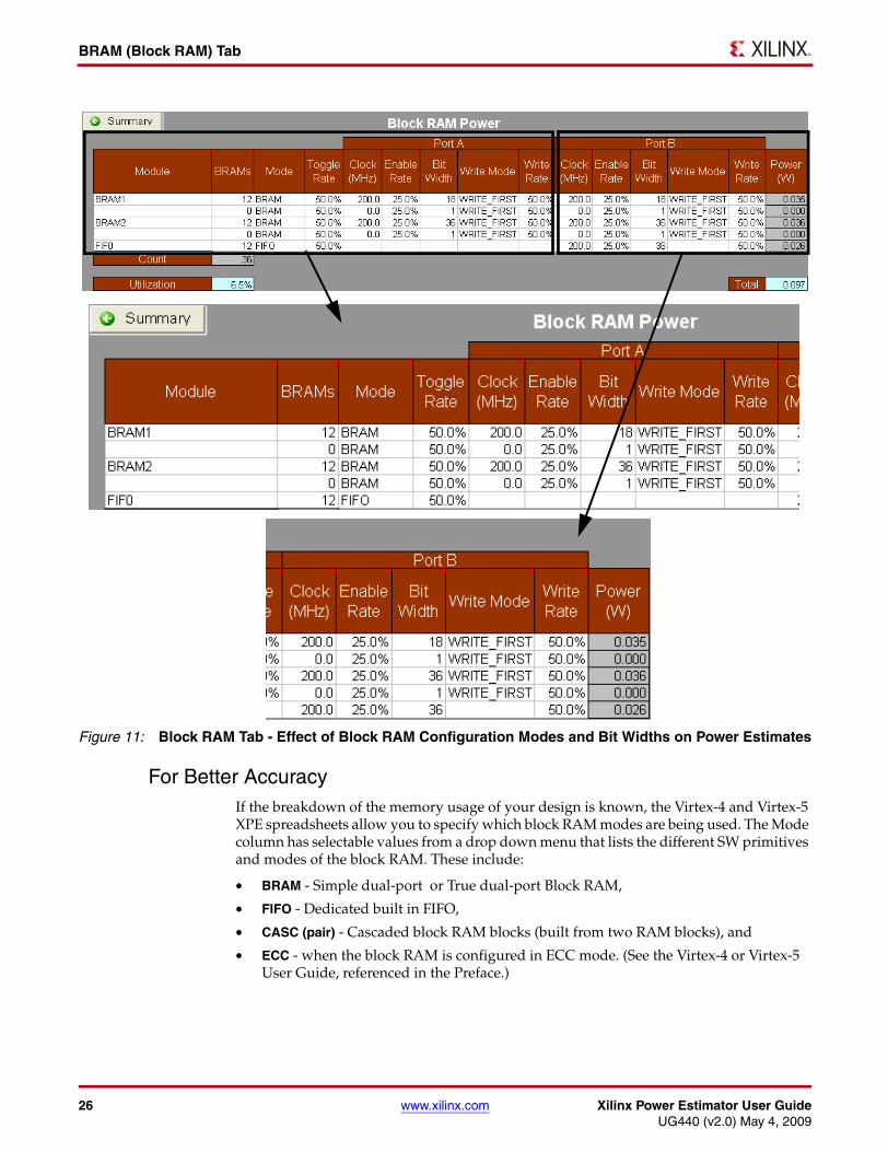
The toggle rate, enable rate, clock frequency, and number of blocks also should be specified in the BRAM tab of the XPE spreadsheet. The enable rate specifies the percentage of time during which the block RAM ports are enabled for reading and/or writing. To save power, the RAM enable can be driven Low on clock cycles when the block RAM is not used in the design. BRAM Enable Rate, together with Clock Rate, are important parameters that must be considered for power optimization. The enable rate specifies the percentage of time during which the block RAM ports are enabled for reading and/or writing. To save power, the RAM enable can be driven Low on clock cycles when the block RAM is not used in the design.
The write rate represents the percentage of time that each block RAM port performs write operations. The read rate is understood to be 100% – write rate.
Figure 11 illustrates the effect of block RAM configuration modes and bit widths on power estimates.
26 www.xilinx.com Xilinx Power Estimator User GuideUG440 (v2.0) May 4, 2009
BRAM (Block RAM) Tab
X-Ref Target - Figure 11
For Better AccuracyIf the breakdown of the memory usage of your design is known, the Virtex-4 and Virtex-5 XPE spreadsheets allow you to specify which block RAM modes are being used. The Mode column has selectable values from a drop down menu that lists the different SW primitives and modes of the block RAM. These include:
• BRAM - Simple dual-port or True dual-port Block RAM,
• FIFO - Dedicated built in FIFO,
• CASC (pair) - Cascaded block RAM blocks (built from two RAM blocks), and
• ECC - when the block RAM is configured in ECC mode. (See the Virtex-4 or Virtex-5 User Guide, referenced in the Preface.)
Figure 11: Block RAM Tab - Effect of Block RAM Configuration Modes and Bit Widths on Power Estimates
Xilinx Power Estimator User Guide www.xilinx.com 27UG440 (v2.0) May 4, 2009
BRAM (Block RAM) Tab
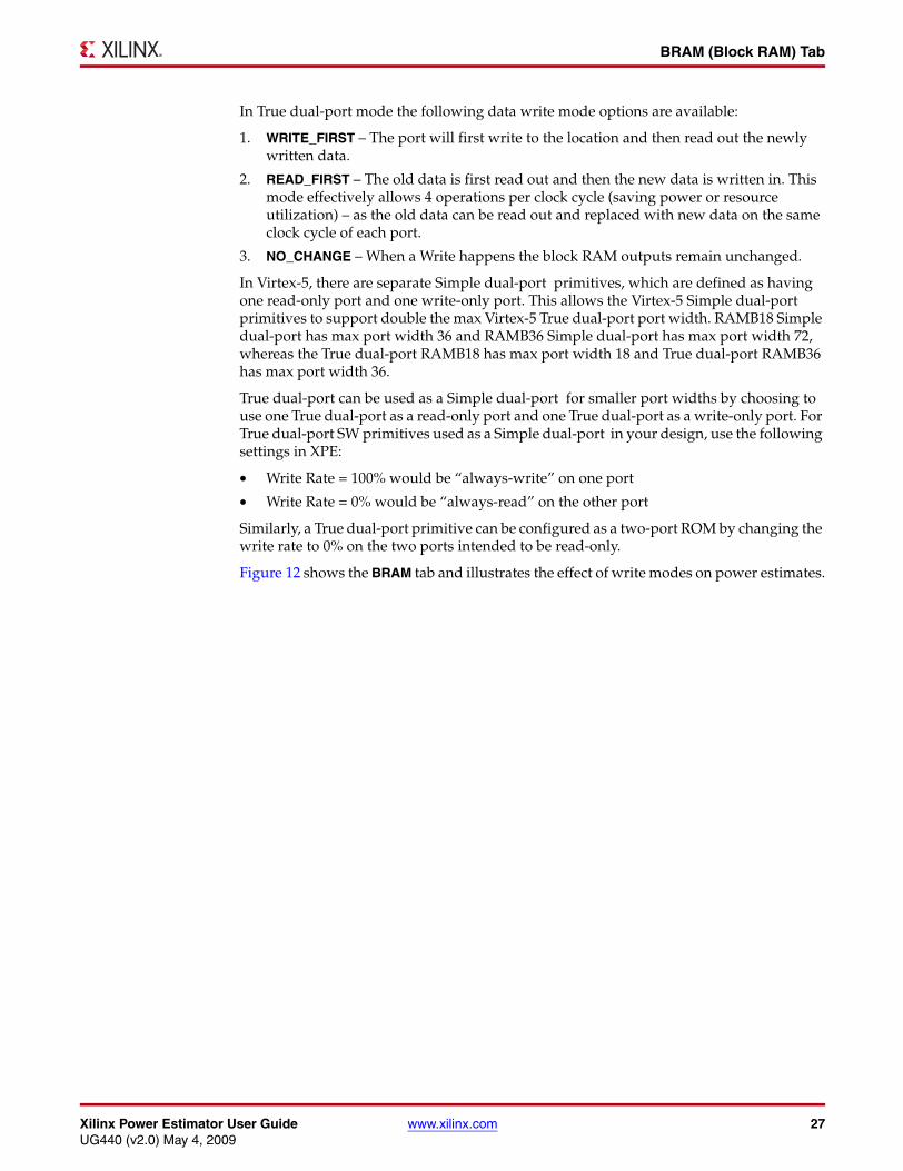
In True dual-port mode the following data write mode options are available:
1. WRITE_FIRST – The port will first write to the location and then read out the newly written data.
2. READ_FIRST – The old data is first read out and then the new data is written in. This mode effectively allows 4 operations per clock cycle (saving power or resource utilization) – as the old data can be read out and replaced with new data on the same clock cycle of each port.
3. NO_CHANGE – When a Write happens the block RAM outputs remain unchanged.
In Virtex-5, there are separate Simple dual-port primitives, which are defined as having one read-only port and one write-only port. This allows the Virtex-5 Simple dual-port primitives to support double the max Virtex-5 True dual-port port width. RAMB18 Simple dual-port has max port width 36 and RAMB36 Simple dual-port has max port width 72, whereas the True dual-port RAMB18 has max port width 18 and True dual-port RAMB36 has max port width 36.
True dual-port can be used as a Simple dual-port for smaller port widths by choosing to use one True dual-port as a read-only port and one True dual-port as a write-only port. For True dual-port SW primitives used as a Simple dual-port in your design, use the following settings in XPE:
• Write Rate = 100% would be “always-write” on one port
• Write Rate = 0% would be “always-read” on the other port
Similarly, a True dual-port primitive can be configured as a two-port ROM by changing the write rate to 0% on the two ports intended to be read-only.
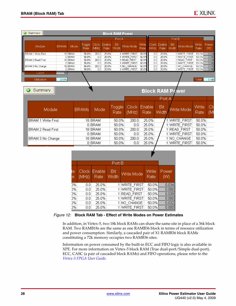
Figure 12 shows the BRAM tab and illustrates the effect of write modes on power estimates.
28 www.xilinx.com Xilinx Power Estimator User GuideUG440 (v2.0) May 4, 2009
BRAM (Block RAM) Tab
X-Ref Target - Figure 12
In addition, in Virtex-5, two 18k block RAMs can share the same site in place of a 36k block RAM. Two RAMB18s are the same as one RAMB36 block in terms of resource utilization and power consumption. Similarly, a cascaded pair of X1 RAMB36 block RAMs constituting a 72k memory occupies two RAMB36 sites.
Information on power consumed by the built-in ECC and FIFO logic is also available in XPE. For more information on Virtex-5 block RAM (True dual-port/Simple dual-port), ECC, CASC (a pair of cascaded block RAMs) and FIFO operations, please refer to the Virtex-5 FPGA User Guide.
Figure 12: Block RAM Tab - Effect of Write Modes on Power Estimates
Xilinx Power Estimator User Guide www.xilinx.com 29UG440 (v2.0) May 4, 2009
DCM, PMCD, and PLL Tabs
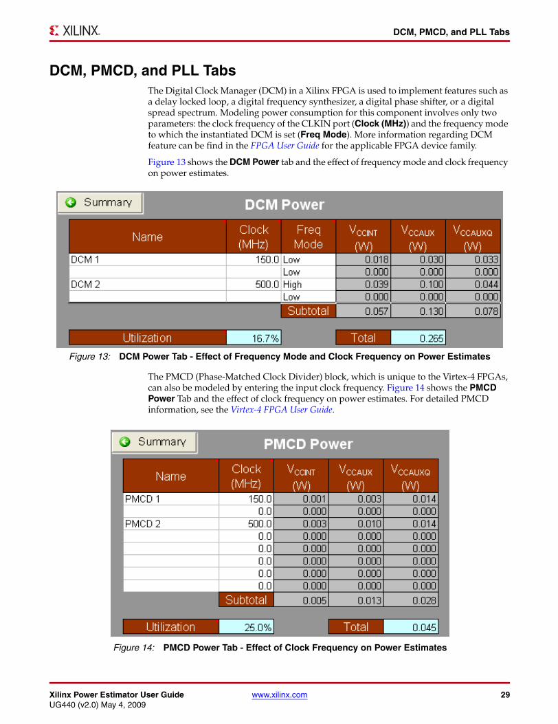
DCM, PMCD, and PLL TabsThe Digital Clock Manager (DCM) in a Xilinx FPGA is used to implement features such as a delay locked loop, a digital frequency synthesizer, a digital phase shifter, or a digital spread spectrum. Modeling power consumption for this component involves only two parameters: the clock frequency of the CLKIN port (Clock (MHz)) and the frequency mode to which the instantiated DCM is set (Freq Mode). More information regarding DCM feature can be find in the FPGA User Guide for the applicable FPGA device family.
Figure 13 shows the DCM Power tab and the effect of frequency mode and clock frequency on power estimates. X-Ref Target - Figure 13
The PMCD (Phase-Matched Clock Divider) block, which is unique to the Virtex-4 FPGAs, can also be modeled by entering the input clock frequency. Figure 14 shows the PMCD Power Tab and the effect of clock frequency on power estimates. For detailed PMCD information, see the Virtex-4 FPGA User Guide.X-Ref Target - Figure 14
Figure 13: DCM Power Tab - Effect of Frequency Mode and Clock Frequency on Power Estimates
Figure 14: PMCD Power Tab - Effect of Clock Frequency on Power Estimates
30 www.xilinx.com Xilinx Power Estimator User GuideUG440 (v2.0) May 4, 2009
DCM, PMCD, and PLL Tabs
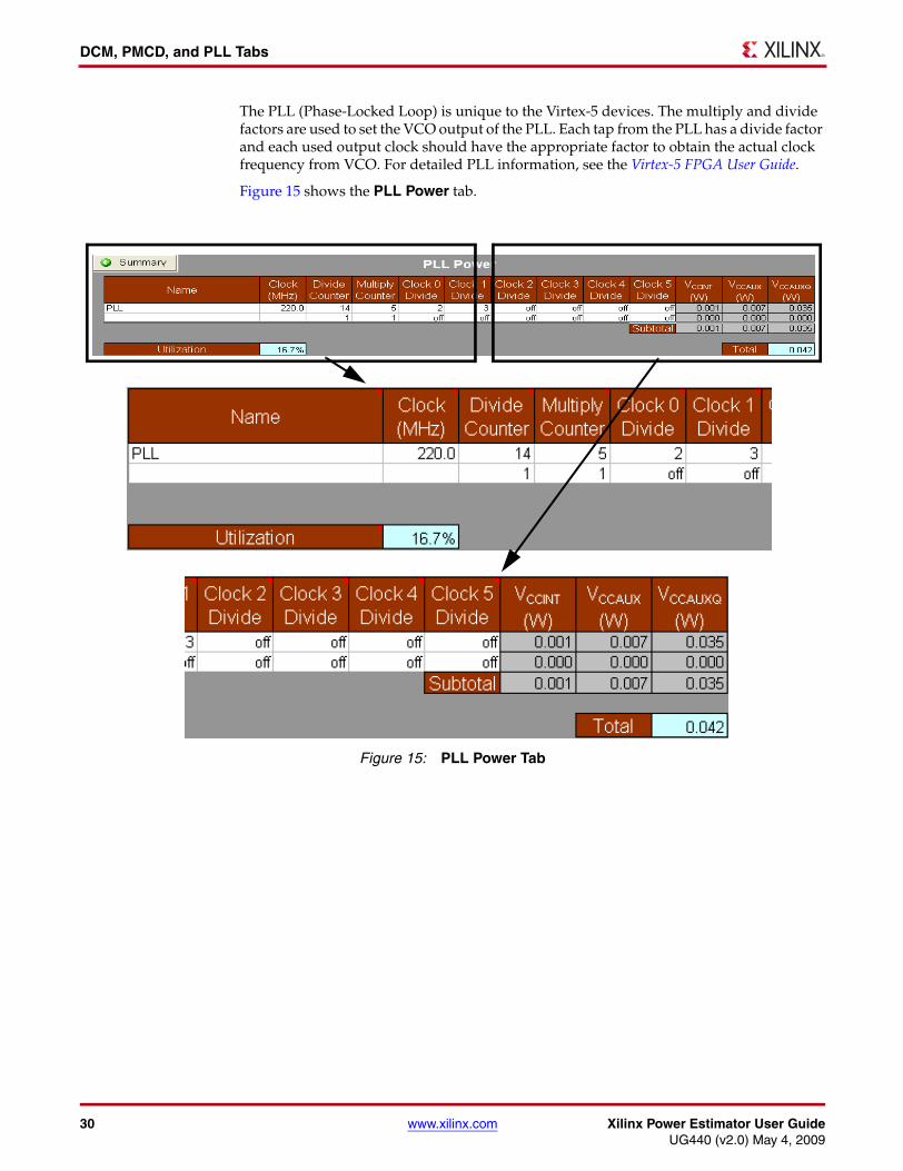
The PLL (Phase-Locked Loop) is unique to the Virtex-5 devices. The multiply and divide factors are used to set the VCO output of the PLL. Each tap from the PLL has a divide factor and each used output clock should have the appropriate factor to obtain the actual clock frequency from VCO. For detailed PLL information, see the Virtex-5 FPGA User Guide.
Figure 15 shows the PLL Power tab. X-Ref Target - Figure 15
Figure 15: PLL Power Tab
Xilinx Power Estimator User Guide www.xilinx.com 31UG440 (v2.0) May 4, 2009
MULT and DSP48 Tabs
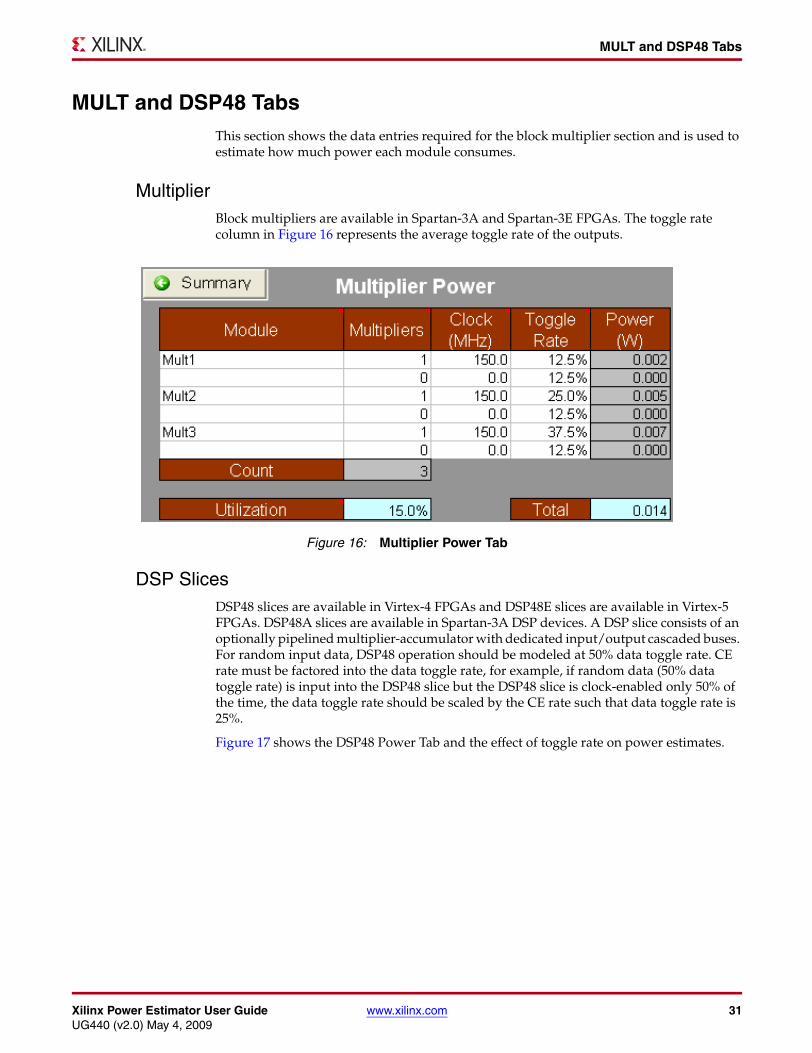
MULT and DSP48 TabsThis section shows the data entries required for the block multiplier section and is used to estimate how much power each module consumes.
MultiplierBlock multipliers are available in Spartan-3A and Spartan-3E FPGAs. The toggle rate column in Figure 16 represents the average toggle rate of the outputs. X-Ref Target - Figure 16
DSP SlicesDSP48 slices are available in Virtex-4 FPGAs and DSP48E slices are available in Virtex-5 FPGAs. DSP48A slices are available in Spartan-3A DSP devices. A DSP slice consists of an optionally pipelined multiplier-accumulator with dedicated input/output cascaded buses. For random input data, DSP48 operation should be modeled at 50% data toggle rate. CE rate must be factored into the data toggle rate, for example, if random data (50% data toggle rate) is input into the DSP48 slice but the DSP48 slice is clock-enabled only 50% of the time, the data toggle rate should be scaled by the CE rate such that data toggle rate is 25%.
Figure 17 shows the DSP48 Power Tab and the effect of toggle rate on power estimates.
Figure 16: Multiplier Power Tab
32 www.xilinx.com Xilinx Power Estimator User GuideUG440 (v2.0) May 4, 2009
MULT and DSP48 Tabs
X-Ref Target - Figure 17
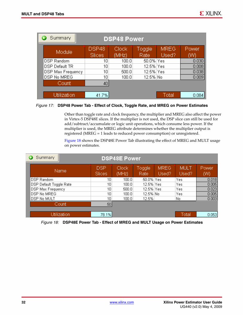
Other than toggle rate and clock frequency, the multiplier and MREG also affect the power in Virtex-5 DSP48E slices. If the multiplier is not used, the DSP slice can still be used for add/subtract/accumulate or logic unit operations, which consume less power. If the multiplier is used, the MREG attribute determines whether the multiplier output is registered (MREG = 1 leads to reduced power consumption) or unregistered.
Figure 18 shows the DSP48E Power Tab illustrating the effect of MREG and MULT usage on power estimates.X-Ref Target - Figure 18
Figure 17: DSP48 Power Tab - Effect of Clock, Toggle Rate, and MREG on Power Estimates
Figure 18: DSP48E Power Tab - Effect of MREG and MULT Usage on Power Estimates
Xilinx Power Estimator User Guide www.xilinx.com 33UG440 (v2.0) May 4, 2009
MGT and GT Tabs
MGT and GT TabsThis section describes the data entries required for the block RocketIO MGT (Multi-Gigabit Transcevier) tabs which are used to estimate how much power the MGTs consume.
MGTs are available in the Virtex-4 and Virtex-5 architectures. The MGT block requires separate, well filtered, power supplies. The supply nomenclature and the voltages are different for each of the families.
For Virtex-5 devices two types of MGTs are supported: GTP and GTX.
• GTP operates up to 3.75Gb/s. GTP transceivers s are available in the LXT and SXT members of the Virtex-5 family.
• GTX operates up to 6.50Gb/s. GTX transceivers are available in the FXT members of the Virtex-5 family.
For details on MGTs, see these User Guides:
• Virtex-4 RocketIO Multi-Gigabit Transceiver User Guide
• Virtex-5 RocketIO GTX Transceiver User Guide
• Virtex-5 RocketIO GTP Transceiver User Guide
The power supplies used for Virtex-5 MGTs (GTP and GTX) and the primary parameter defining the current are shown in Table 2.
The XPE spreadsheet automatically selects the correct MGT type (GTP or GTX) depending on the device chosen in the Summary tab. Each MGT comprises a Transceiver, both Transmitter and Receiver.
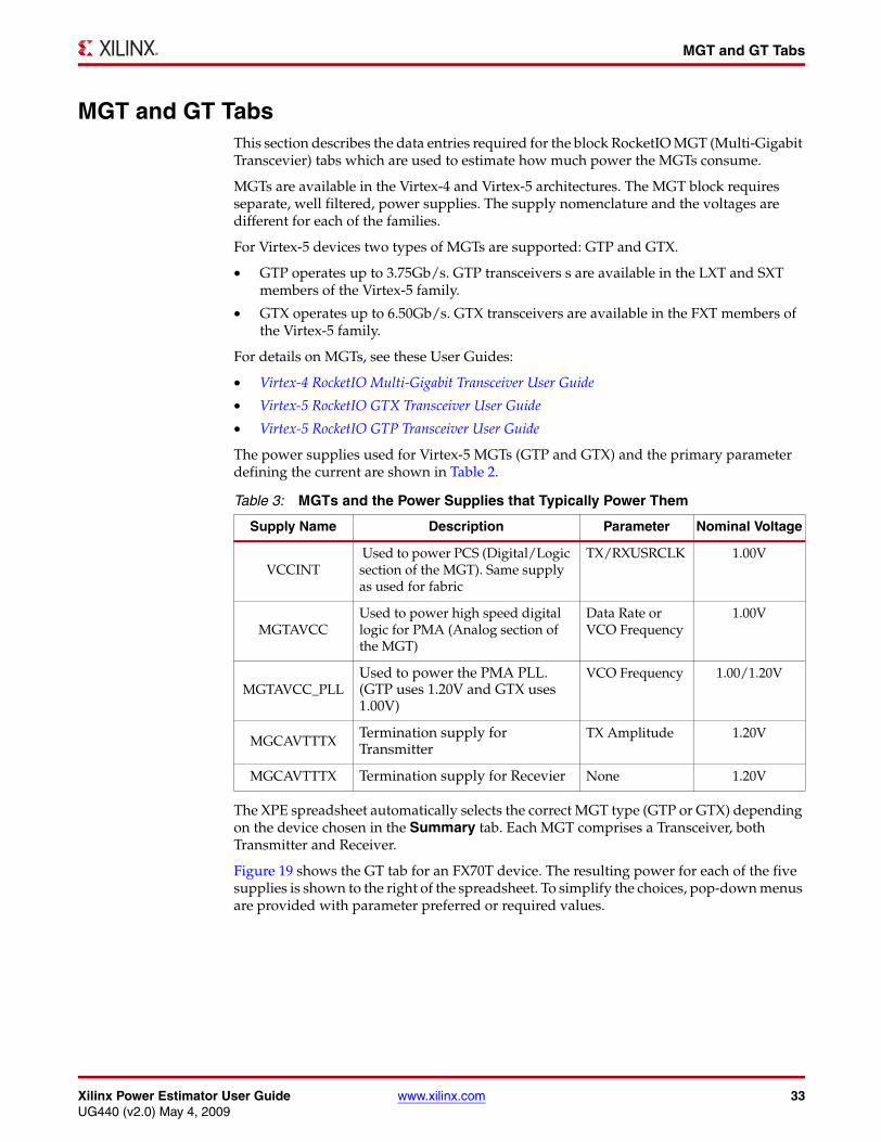
Figure 19 shows the GT tab for an FX70T device. The resulting power for each of the five supplies is shown to the right of the spreadsheet. To simplify the choices, pop-down menus are provided with parameter preferred or required values.
Table 3: MGTs and the Power Supplies that Typically Power Them
Supply Name Description Parameter Nominal Voltage
VCCINT Used to power PCS (Digital/Logic section of the MGT). Same supply as used for fabric
TX/RXUSRCLK 1.00V
MGTAVCCUsed to power high speed digital logic for PMA (Analog section of the MGT)
Data Rate or VCO Frequency
1.00V
MGTAVCC_PLLUsed to power the PMA PLL. (GTP uses 1.20V and GTX uses 1.00V)
VCO Frequency 1.00/1.20V
MGCAVTTTXTermination supply for Transmitter
TX Amplitude 1.20V
MGCAVTTTX Termination supply for Recevier None 1.20V
34 www.xilinx.com Xilinx Power Estimator User GuideUG440 (v2.0) May 4, 2009
MGT and GT Tabs
X-Ref Target - Figure 19
User defined columns and rows in the spreadsheet are.
• GTXs
You can select up to the maximum number of available GTX transceivers for the chosen device (Count). The FX70T device has 8 GTX_DUAL or 16 GTXs which represent 100% of the MGT resources (Utilization).
• Data Rate (GHz)
Although the device can operate over a wide range of datarates up to 6.50Gb/s, the most popular data rates have been included in the tool. Select the data rate closest to your application. More power is consumed by the MGTs at higher data rates.
• Operational Mode
By using power management capability built into the device, the MGT can be operated as a Transceiver (both Transmitter and Recevier), a Transmitter only, or a Receiver only. Note that the Virtex-5 MGT uses a shared PLL architecture so the PLL supply will indicate the same current if either the Transmitter or the Receiver is used.
• Data Path
The datapath is the byte width of data used in the PCS; either 8 or 10bits. Along with the data rate, this parameter is used to determine TX and RX USRCLK frequency which determines the PCS power.
• TX O/P
The TX amplitude can be adjusted on the MGT to suit a particular application (channel attenuation). TX O/P is the differential output voltage and corresponds to eight settings, 0-7, on the TXDIFFCTRL port. TX O/P only affects the MGTAVTTTX supply.
• VCO (GHz)
For GTX the PLL operates in the range 1.50-3.25GHz. The VCO frequency is automatically selected when you enter the data rate. Typically VCO frequency = Data Rate / 2.
Some data rates allow for two values of VCO frequency. For example, Data Rate = 3.2Gb/s permits the VCO to be operated at either 3.20GHz or 1.60GHz. Operating the
Figure 19: GT Power Tab Illustrating the Effect of Data Rate and TX O/P Usage on Power Estimates
Xilinx Power Estimator User Guide www.xilinx.com 35UG440 (v2.0) May 4, 2009
EMAC and TEMAC Tabs
VCO at higher frequencies may results in lower jitter, but operating the VCO at lower frequency will result in lower power for the MGTAVCC_PLL supply.
• Unused GTX_DUALs
Use Unused GTP/X_DUALs to specify how you wish the unused GTP/X transceivers to be powered. Selections are either Powered or Grounded.
♦ Powered - Use this setting if you intend to power up the unused GTX transceivers. This setting is required if you use Clock Forwarding since the MGTCLK requires filtered power to provide a copy of the clock to the used GTs.
♦ Grounded - Use this option for the lowest GTP or GTX power. With the exception of AVCC for GTP, the supplies for the unused GTPs or GTXs can be connected to GROUND. For GTP, AVCC is required to be powered up to maintain the functionality of the Boundary Scan Chain. For GTX all supplies can be grounded without affecting the functionality of the Bound.
Note: For Virtex-5 LXT and SXT devices, XPE assumes that you require the Boundary Scan Chain to be functional and the AVCC supply will show static current.
For details on how to connect unused GTP and GTX transceivers, see the applicable User Guide:
• Virtex-5 RocketIO GTX Transceiver User Guide
• Virtex-5 RocketIO GTP Transceiver User Guide
EMAC and TEMAC TabsThe Virtex-4 and Virtex-5 device families contain Tri-Mode Embedded Ethernet Media Access Controller (MAC) blocks, which are used in Ethernet applications. The Ethernet MACs are paired within a TEMAC block, share a common host and DCR interface, but are independently configurable to meet all common Ethernet system connectivity needs.
For TEMAC information, see the Virtex-4 FPGA Embedded Tri-Mode Ethernet MAC User Guide or the Virtex-5 FPGA Embedded Tri-Mode Ethernet MAC User Guide.
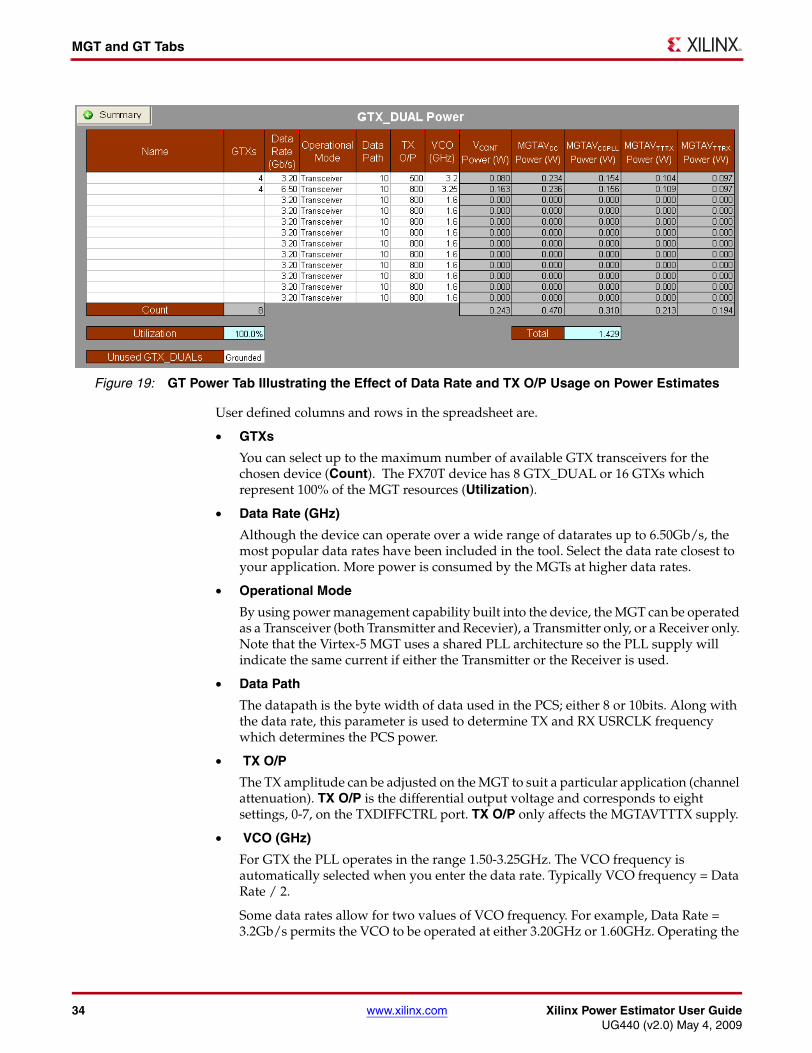
In XPE, the Virtex-4 spreadsheet contains an EMAC tab and the Virtex-5 spreadsheet contains a TEMAC tab. For power estimation, you need only enter the operating clock frequency of the EMAC (See Figure 20). You will need to know the mode and operating speed to obtain the correct clock frequency.X-Ref Target - Figure 20
Figure 20: TEMAC Power Tab
36 www.xilinx.com Xilinx Power Estimator User GuideUG440 (v2.0) May 4, 2009
PCIE Tab
PCIE TabThe Virtex-5 device family contains Integrated Endpoint Block for PCI Express® designs (integrated Endpoint block). The Virtex-5 FPGA Integrated Endpoint block provides the full functionality of the Transaction Layer, the Data Link Layer, the Physical Layer, and the Configuration.
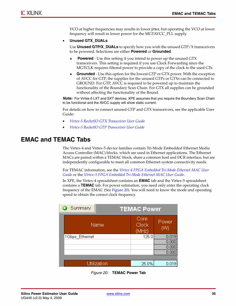
Space as per the PCI Express® Base Specification Revision 1.1. The integrated Endpoint block has two synchronous clock domains: core_clk and user_clk. The user_clk domain allows user logic in the fabric to run at a slower speed than the integrated Endpoint block in x1, x2, or x4 modes. For power estimation you need to enter the core and user clock frequencies and the number of lanes used (See Figure 21).
For detailed PCIE information, see the Virtex-5 FPGA Integrated Endpoint Block for PCI Express Designs User Guide.X-Ref Target - Figure 21
PPC405 and PPC440 (PowerPC) TabsThe Virtex-4 and Virtex-5 device families contain high-performance PowerPC® microprocessor embedded blocks.
The Virtex-4 device family contains 32-bit PowerPC® 405 microprocessors. For power estimation the main components of the PPC405 embedded processor block are the processor, the processor local bus (PLB), and the on-chip memory (OCM). In the PPC tab (See Figure 22), you will need to set the correct clock frequencies for the processor, PLB, DCR (Device Control Register), and the OCM.
For detailed PPC405 information, see the PowerPC 405 Processor Block Reference Guide.
Figure 21: PCIE Power Tab
Xilinx Power Estimator User Guide www.xilinx.com 37UG440 (v2.0) May 4, 2009
Conclusion
X-Ref Target - Figure 22
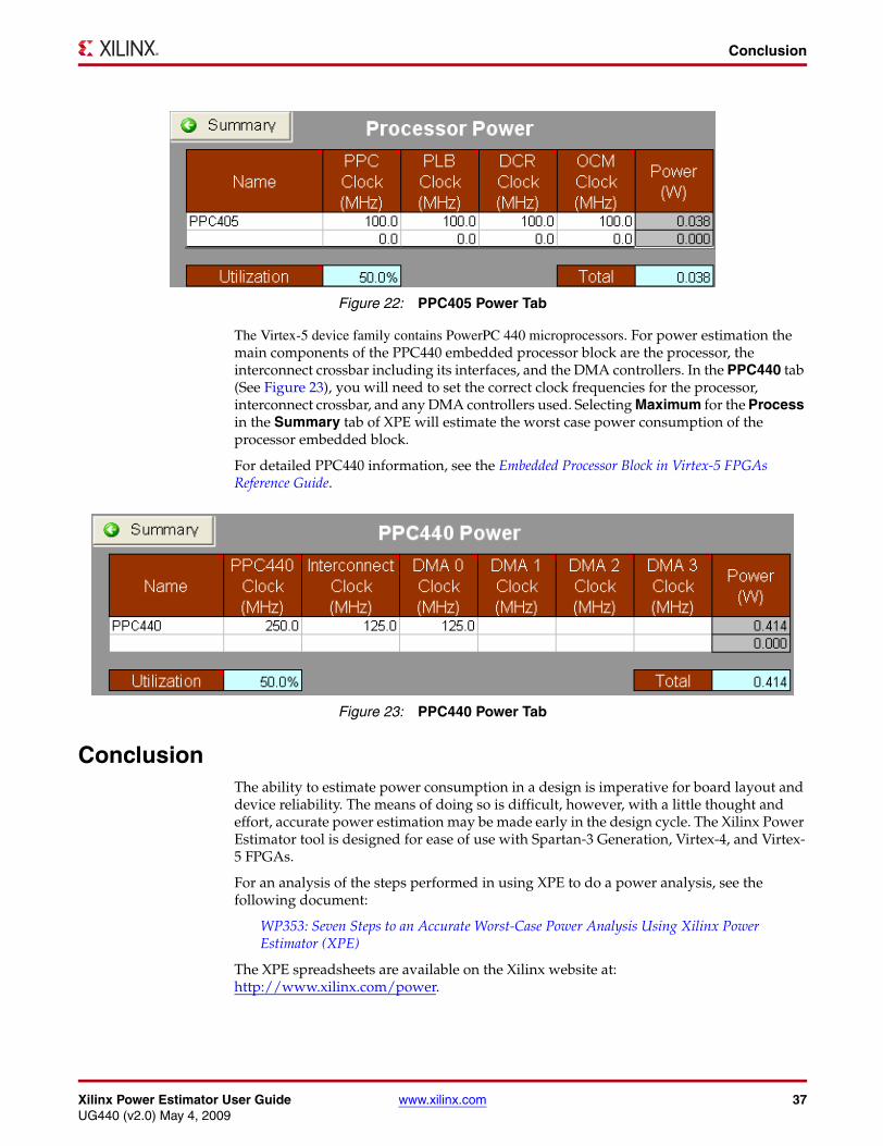
The Virtex-5 device family contains PowerPC 440 microprocessors. For power estimation the main components of the PPC440 embedded processor block are the processor, the interconnect crossbar including its interfaces, and the DMA controllers. In the PPC440 tab (See Figure 23), you will need to set the correct clock frequencies for the processor, interconnect crossbar, and any DMA controllers used. Selecting Maximum for the Process in the Summary tab of XPE will estimate the worst case power consumption of the processor embedded block.
For detailed PPC440 information, see the Embedded Processor Block in Virtex-5 FPGAs Reference Guide.X-Ref Target - Figure 23
ConclusionThe ability to estimate power consumption in a design is imperative for board layout and device reliability. The means of doing so is difficult, however, with a little thought and effort, accurate power estimation may be made early in the design cycle. The Xilinx Power Estimator tool is designed for ease of use with Spartan-3 Generation, Virtex-4, and Virtex-5 FPGAs.
For an analysis of the steps performed in using XPE to do a power analysis, see the following document:
WP353: Seven Steps to an Accurate Worst-Case Power Analysis Using Xilinx Power Estimator (XPE)
The XPE spreadsheets are available on the Xilinx website at: http://www.xilinx.com/power.
Figure 22: PPC405 Power Tab
Figure 23: PPC440 Power Tab

38 www.xilinx.com Xilinx Power Estimator User GuideUG440 (v2.0) May 4, 2009
Conclusion