Embed Size (px)
Citation preview
XAPP891 (v2.0) December 18, 2013 www.xilinx.com 1
© Copyright 2012–2013 Xilinx, Inc. Xilinx, the Xilinx logo, Artix, ISE, Kintex, Spartan, Virtex, Vivado, Zynq, and other designated brands included herein are trademarks of Xilinx in the United States and other countries. AMBA and ARM are registered trademarks of ARM in the EU and other countries. All other trademarks are the property of their respective owners.
ies
Summary This application note demonstrates the performance measurement of the Xilinx universal serial bus 2.0 (USB 2.0) [Ref 1] high-speed device with an advanced microcontroller bus architecture (AMBA®) advanced eXtensible interface (AXI) for bulk and isochronous transactions. The test system generated is based on a Kintex®-7 FPGA and Zynq®-7000 All Programmable SoC. The performance is measured with two separate host drivers for bulk and isochronous transactions. This application note describes how to develop a USB system and corresponding ELF files for bulk and isochronous transactions. It is assumed that you have general knowledge of the Xilinx Vivado® Design Suite and Vivado IP Integrator [Ref 2].
Introduction The AXI USB 2.0 device enables USB connectivity for a design using a minimal amount of resources. This interface is suitable for USB-centric, high-performance designs, bridges, and legacy port replacement operations. The USB 2.0 protocol multiplexes many devices over a single, half-duplex, serial bus. The AXI USB 2.0 device runs at 480 Mb/s (high speed) or at 12 Mb/s (full speed), and is designed to be plug-and-play. The host controls the bus and sends tokens to the device specifying the required action. The AXI USB 2.0 device supports up to eight endpoints, including default control endpoints that are sources or sinks of data. Endpoint 0 of the USB 2.0 device is used to enumerate the device with control transactions.
The seven user endpoints of the AXI USB 2.0 device can be configured as bulk, interrupt, or isochronous. Also, endpoints can be configured as input (to the host) or output (from the host). Each of these endpoints has two ping-pong buffers of the same size for endpoint data. The user endpoints data buffers are unidirectional and are configured by the endpoint configuration and status register of the respective endpoint. The size of the buffers can be configured from 0 to 512 bytes for bulk, 64 bytes for interrupt, and up to 1,024 bytes for isochronous endpoints.
This application note is targeted to demonstrate USB bulk and isochronous transactions performance. The following elements are used in the application:
• A MicroBlaze™ processor or Zynq-7000 device reference system with an AXI USB 2.0 device and DDR controller.
• Executable and linkable format (ELF) files that configure the device as bulk or isochronous endpoints.
• Host application used to measure the USB device performance.
The AXI USB 2.0 device consists of a built-in direct memory access (DMA) controller to transfer the data from endpoint buffers to the memory and vice versa. The USB 2.0 device core consists of a dedicated AXI4 slave interface and an optional AXI4 master interface. The optional master interface is configured through the device parameter Enable DMA Support. When the AXI USB2 Controller is configured with DMA support, the DMA logic is included in the design. When the DMA logic is included, the user endpoint buffer location is not accessible from the AXI slave interface. When the DMA is disabled, the endpoint buffer location can be accessed by the AXI slave interface.
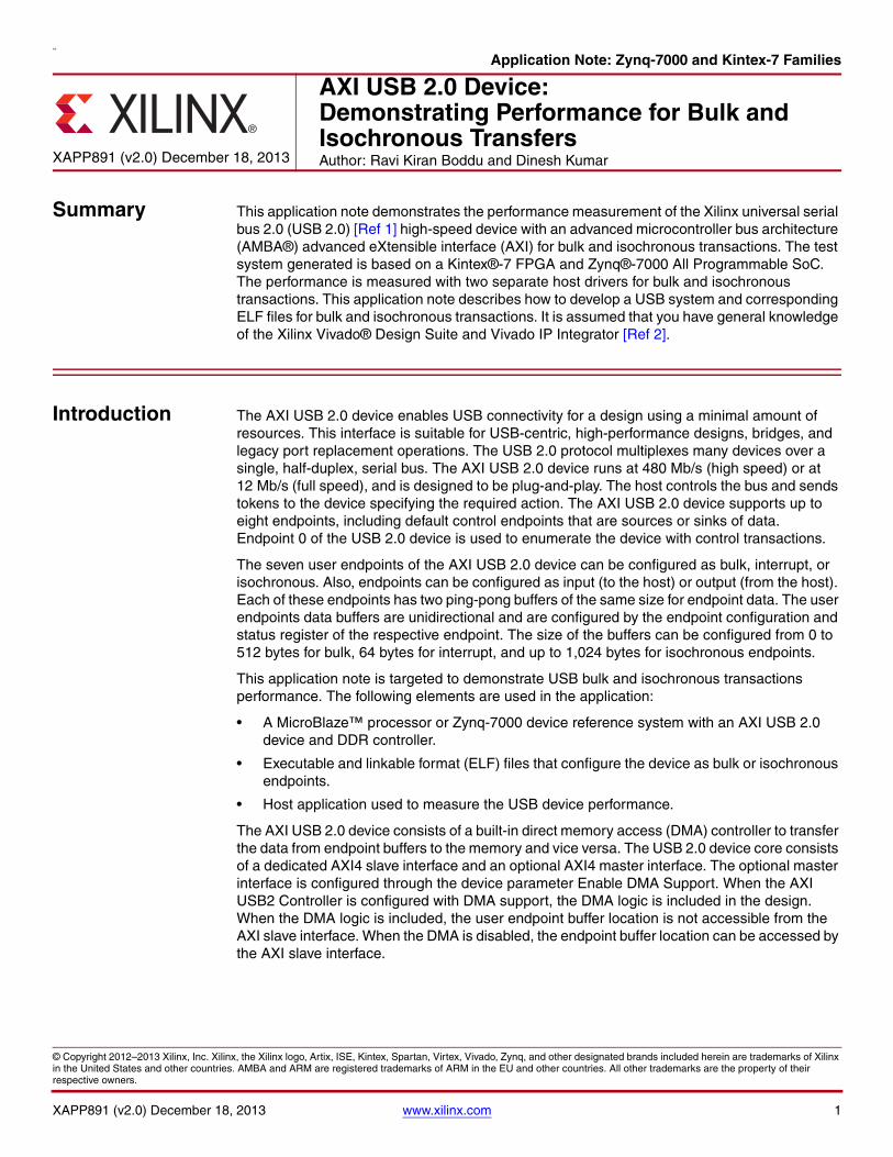
Application Note: Zynq-7000 and Kintex-7 Families
XAPP891 (v2.0) December 18, 2013
AXI USB 2.0 Device: Demonstrating Performance for Bulk and Isochronous TransfersAuthor: Ravi Kiran Boddu and Dinesh Kumar
Mass Storage Application
XAPP891 (v2.0) December 18, 2013 www.xilinx.com 2
Mass Storage Application
The mass storage application uses bulk transactions, which require two endpoint buffers configured as bulk-in and bulk-out endpoints and a maximum packet size set to 512 bytes. The bulk-in endpoint is used to measure the performance for a read operation and the bulk-out endpoint is used to measure the performance for a write operation.
The bulk application initializes the system to enable the USB and UART devices. Responds for device enumeration commands (SET/GET descriptor) from the host. When the enumeration is completed, if the device receives a read request from the host the following occurs.
1. Data is written into the ping/pong buffers present in the USB device through the DMA.
2. Upon receiving the IN token from the host device, the device responds with the data present in the ping/pong buffer.
3. An interrupt is sent to the processor reference system to indicate a buffer free condition for the corresponding endpoint.
4. The processor reference system detects the buffer free interrupt and fills the ping/pong buffer with the next data to send.
5. This process is repeated.
If the device receives a write command, following steps take place.
1. The host device sends an OUT token followed by a data packet.
2. Upon reception of the data, the received data is written into the ping/pong buffer.
3. An interrupt is send to the processor reference system to indicate a buffer full condition for the corresponding end-point.
4. The processor reference system reads the data and stores it into the DDR through the DMA.
5. This procedure is repeated as long as the host sends data.
Isochronous Application
The isochronous application is tested for Read and Write with separate applications. The isoc_in application tests the read operation using isochronous transactions, and the isoc_out application measures the performance of the write operation. The isoc_in application programs the device as a microphone and uses one endpoint as an isochronous In endpoint. The isoc_out application programs the device as a speaker and uses one endpoint as an isochronous out endpoint.
The isochronous application initializes the system to enable the USB and UART devices. Responds for device enumeration commands (SET/GET descriptor) are from the host. After the enumeration is completed, if the device is configured as a microphone, the following steps occur.
1. Data is written into the ping/pong buffers present in the USB device through the DMA.
2. Upon receiving the IN token from the host device, the device responds with data present in the ping/pong buffer.
3. An interrupt is sent to the processor reference system to indicate a buffer free condition for the corresponding endpoint.
4. The processor reference system detects the buffer free interrupt and fills the ping/pong buffer with the next data to send.
5. This process is repeated.
Send Feedback
Core Parameters
XAPP891 (v2.0) December 18, 2013 www.xilinx.com 3
If the device is configured as a speaker, the following steps occur.
1. The host device sends an OUT token followed by a data packet.
2. Upon reception of the data, the received data is written into the ping/pong buffer.
3. An interrupt is send to the processor reference system to indicate a buffer full condition for the corresponding end-point.
4. The processor reference system reads the data and stores it into the DDR through the DMA.
5. This procedure is repeated.
Core Parameters
Table 1 includes the description, name, and usage guidelines for the core parameters.
Hardware Requirements
The hardware boards and additional equipment required for this reference system include:
• Xilinx KC705 or ZC702 production board
• Xilinx USB PHY FMC card with LPC connector
• JTAG platform cable USB
• Two USB mini-B cables
The installed design tools requirements for building and downloading this reference system are:
• Vivado Design Suite 2013.3
• SDK 2013.3
Table 1: Core Parameters
Feature/Description Parameter Name Usage
Use DMA logic Enable DMA Support 1
Choice of PHY reset type ULPI PHY Reset Polarity active_low
Choice of including error logic Enable USB Error Counters 1
Choice of unaligned transaction support Enable Un-aligned Transactions 1
Use HSIC PHY ENABLE HSIC PHY 0
Connect Signal Width Connect Signaling Width 0
Send Feedback
Using AXI USB 2.0 Device
XAPP891 (v2.0) December 18, 2013 www.xilinx.com 4
Using AXI USB 2.0 Device
The AXI USB 2.0 device IP can be connected on an AXI-based system with a 32-bit data width. The IP supports a ULPI interface on the USB PHY side. The IP can be configured in DMA mode or non-DMA mode with the parameter Enable DMA Support. When the DMA is enabled, the AXI master interface is enabled and the AXI4 master interface must be connected to an AXI4 interconnect to which a DDR controller is connected as slave. The interrupt pin of the IP should be connected to the interrupt controller block of the processor system. The parameters used to configure the IP are:
• Enable DMA Support: When set to 1, a built-in DMA block is included in the design along with the AXI4 master interface. The addition of the DMA block disconnects the user endpoint buffers from the AXI slave interface.
• Enable Un-aligned Transactions: When set to 1, data realignment support is added to the design.
• ULPI PHY Reset Polarity: This parameter must be set according to the PHY requirements. When set as ACTIVE_LOW, the ULPI reset generated by the AXI USB 2.0 device IP is an active-Low signal. When set to ACTIVE_HIGH, the ULPI reset generated by the AXI USB 2.0 device IP is an active-High signal.
• Enable USB Error Counters: When set to 1, the USB link error logging counters are added in the design.
• ENABLE HSIC PHY: This parameter enables the HSIC PHY module and adds the HSIC interface at the I/O level. When this parameter is enabled, the ULPI interface is not available at the I/O level.
• Connect Signaling Width: This parameter is valid only when ENABLE HSIC PHY is set to 1. This parameter indicates the number of clock cycle for which connect signaling is sent by the HSIC PHY.
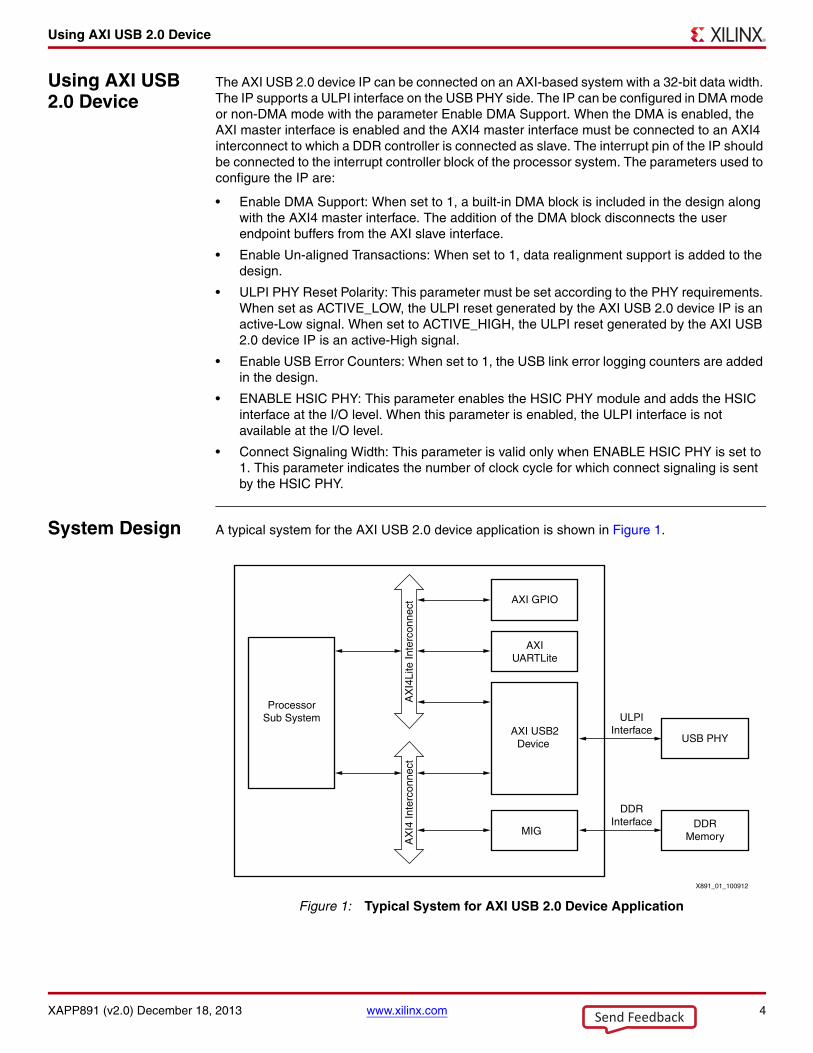
System Design A typical system for the AXI USB 2.0 device application is shown in Figure 1.
X-Ref Target - Figure 1
Figure 1: Typical System for AXI USB 2.0 Device Application
ProcessorSub System
AXI GPIO
AXIUARTLite
AXI USB2Device USB PHY
ULPIInterface
DDRInterface
MIGDDR
Memory
AX
I4Li
te In
terc
onne
ctA
XI4
Inte
rcon
nect
X891_01_100912
Send Feedback
Reference Design Components
XAPP891 (v2.0) December 18, 2013 www.xilinx.com 5
The system is based on AXI, which is a standardized IP interface protocol based on the AMBA specification. The AXI interfaces used in the reference design consist of AXI4 memory mapped and AXI4-Lite. A clock generator and processor system reset block supplies clocks and resets throughout the system. High-level control of the system is provided by an embedded MicroBlaze or ARM® based processor subsystem containing I/O peripherals and processor support IP.
To optimize the system to balance performance and area, multiple AXI interconnect blocks are used to implement segmented or hierarchical AXI interconnect networks with each AXI interconnect block individually tuned and optimized.
Reference Design Components
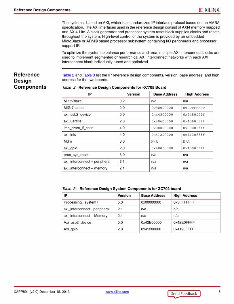
Table 2 and Table 3 list the IP reference design components, version, base address, and high address for the two boards.
Table 2: Reference Design Components for KC705 Board
IP Version Base Address High Address
MicroBlaze 9.2 n/a n/a
MIG 7 series 2.0 0x80000000 0xBFFFFFFF
axi_usb2_device 5.0 0x44800000 0x4480ffff
axi_uartlite 2.0 0x40600000 0x4060ffff
lmb_bram_if_cntlr 4.0 0x00000000 0x00001fff
axi_intc 4.0 0x41200000 0x4120ffff
Mdm 3.0 N/A N/A
axi_gpio 2.0 0x40000000 0x4000ffff
proc_sys_reset 5.0 n/a n/a
axi_interconnect – peripheral 2.1 n/a n/a
axi_interconnect – memory 2.1 n/a n/a
Table 3: Reference Design System Components for ZC702 board
IP Version Base Address High Address
Processing_ system7 5.3 0x00000000 0x3FFFFFFF
axi_interconnect - peripheral 2.1 n/a n/a
axi_interconnect – Memory 2.1 n/a n/a
Axi_usb2_device 5.0 0x42E00000 0x42E0FFFF
Axi_gpio 2.0 0x41200000 0x4120FFFF
Send Feedback
Hardware Systems
XAPP891 (v2.0) December 18, 2013 www.xilinx.com 6
Hardware Systems A ready-to-use system BIT file and ELF file are provided with this application note for the USB
device and the MicroBlaze or ARM processor application for KC705/ZC702 boards respectively. The hardware system consists of a USB 2.0 device system with a processor sub system and a 7 series FPGA DDR3 controller.
To create a reference system:
1. Unzip the given zip file XAPP_891.zip in the local directory.
Follow the next steps to create the project for the KC705 or ZC702 Board.Example:
2. Launch the Vivado Design Suite.
3. Select Create New Project and click Next.
4. Select the project name and path and click Next.
5. Select RTL Project to permit running the example design and click Do not specify sources at this time. Click Next.
6. Select the boards option and then click Kintex-7 FPGA KC705 Evaluation platform or ZYNC-7 ZC702 Evaluation Board.
7. Click Next and then click Finish.
8. Go to HW/KC705 or HW/ZC702 depending on the board selected.
9. If the board selected is KC705, source the file kc705_usb_system.tcl from the Tcl console with the command source kc705_usb_system.tcl.
10. If the board selected is ZC702, source the file zc702_usb_system.tcl from the Tcl console with the command source zc702_usb_system.tcl.
11. The Tcl file creates a BD design and automatically instantiates the required components, and creates connections.
12. Right-click the design_1.bd on the Sources panel and click Create HDL Wrapper.
13. Run synthesis, implementation and bitstream generation.
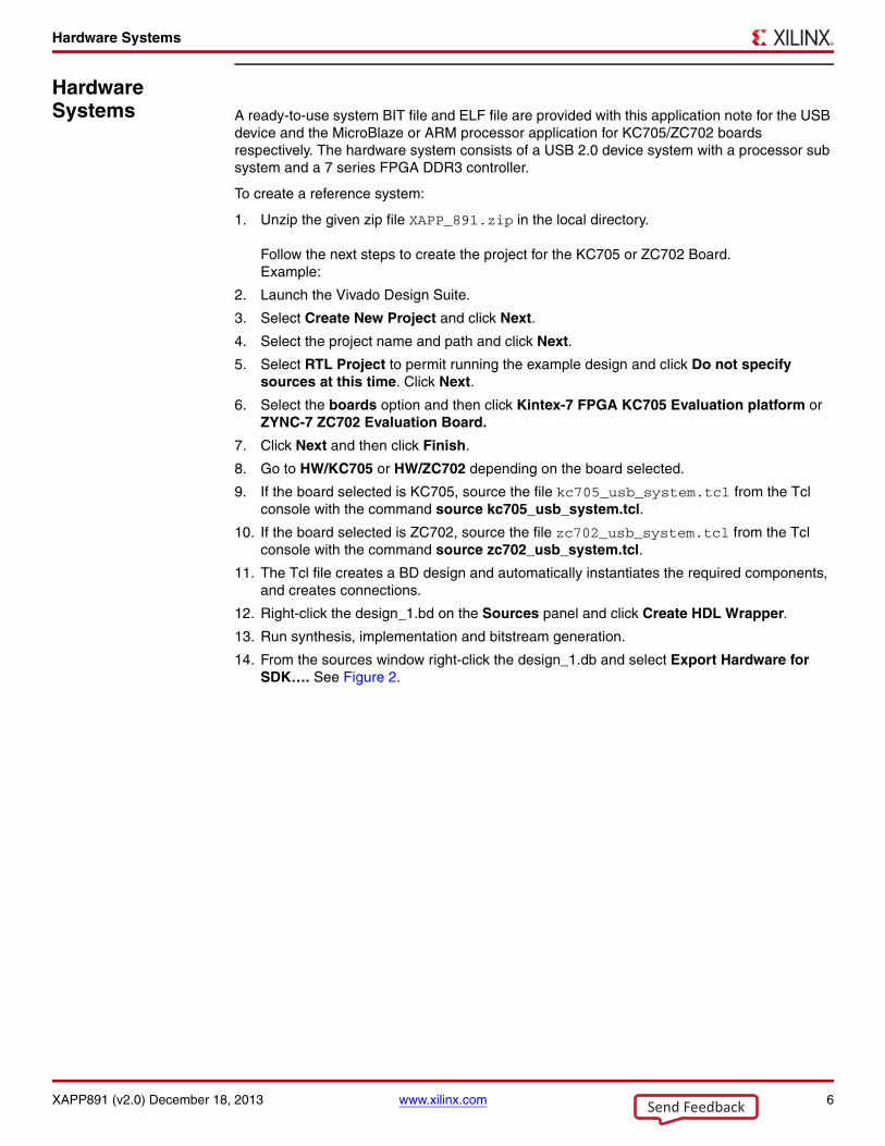
14. From the sources window right-click the design_1.db and select Export Hardware for SDK…. See Figure 2.
Send Feedback
Hardware Systems
XAPP891 (v2.0) December 18, 2013 www.xilinx.com 7
15. Select the Launch SDK check-box and click OK. After completing the processing of the files, SDK is opened.
X-Ref Target - Figure 2
Figure 2: Export Hardware for SDK
Send Feedback
Creating an ELF File
XAPP891 (v2.0) December 18, 2013 www.xilinx.com 8
Creating an ELF File
The following steps describe how to create an ELF file for bulk transactions. These same steps can be used to create ELF files for isochronous In and Out transactions. The source files are located in bulk, isoc_in, and isoc_out folders in the SW/Device_Files directory.
1. Select the Export and Launch option from the pop-up window.
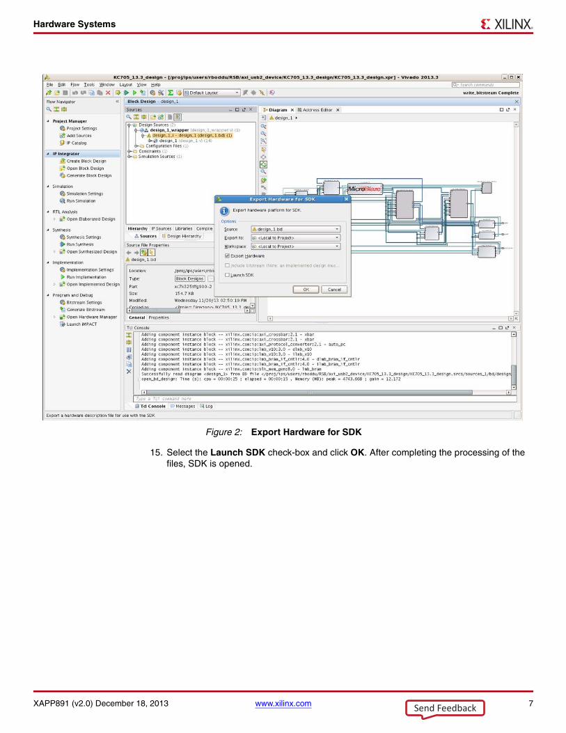
2. When the SDK is open, create an application project for a bulk endpoint application by selecting File > New > Application Project. See Figure 3.
3. Enter bulk_perfmon for the project name.
4. Select the Use default location check box.
5. Set OS Platform to Standalone, Language to C, and Board Support Package to Create New. Click Next.
X-Ref Target - Figure 3
Figure 3: Creating New Project
Send Feedback
Installing Host Side Driver
XAPP891 (v2.0) December 18, 2013 www.xilinx.com 9
6. Select Empty application from Available Templates, and click Finish.
7. From the Project Explorer window, select the src folder under the bulk_perfmon project.
8. Right-click the SRC directory and click Import.
9. Select General > File System and click Next.
10. Browse to the directory SW/Device_Files/bulk and click OK.
11. Select the following files and click Finish:
• xusb_cp9.c
• xusb_cp9.h
• xusb_storage.c
• xusb_storage.h
• xusb_types.h
Installing Host Side Driver
This section describes how to install the host side driver.
Software Requirements
The USB bulk performance monitor has the following software requirements.
• Windows XP (SP3) or higher (32-bit or 64-bit)
• NET Framework 4
Installing the Driver
Separate applications are provided for bulk and isochronous transaction performance measurement. For the isochronous transactions performance measurements, go to the SW/Host_Files/USBISOC_Setup directory. For bulk transaction performance measurements, go to the SW/Host_Files/USBBulk_Setup/ directory.
Double-click Xilinx USB Perfmon Setup x86.msi for a 32-bit machine or Xilinx USB Perfmon Setup x64.msi for a 64-bit machine. Follow the instructions to complete the installation.
Note: For Windows 7 64-bit, after starting the PC and when Windows starts loading, keep pressing the F8 key to open the Advanced Boot Options. In the Advanced Boot Options prompt, disable the Disable Driver Signature Enforcement by setting it to No.
Note: Ensure that the board is configured with a *.bit file and that the *.elf file is loaded before installing the drivers.
If the application does not work, load the MicroBlaze processor application again. It might need to be loaded several times until it works (maximum 2-3 times.)
Hardware Requirements
To demonstrate the USB bulk application, the following hardware components are required:
• KC705 or ZC702 board with power adapter
• One Xilinx USB PHY FMC card (HW-FMC-006-USB-G)
• Two USB cables (2 x USBA/MiniB)
• One JTAG platform USB cable OR 1 x USBA/Micro B cable
Send Feedback
Installing Host Side Driver
XAPP891 (v2.0) December 18, 2013 www.xilinx.com 10
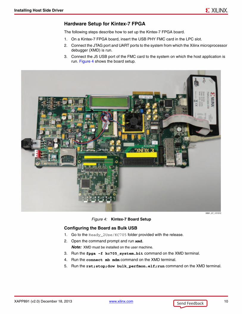
Hardware Setup for Kintex-7 FPGA
The following steps describe how to set up the Kintex-7 FPGA board.
1. On a Kintex-7 FPGA board, insert the USB PHY FMC card in the LPC slot.
2. Connect the JTAG port and UART ports to the system from which the Xilinx microprocessor debugger (XMD) is run.
3. Connect the J5 USB port of the FMC card to the system on which the host application is run. Figure 4 shows the board setup.
Configuring the Board as Bulk USB
1. Go to the Ready_2Use/KC705 folder provided with the release.
2. Open the command prompt and run xmd.
Note: XMD must be installed on the user machine.
3. Run the fpga -f kc705_system.bit command on the XMD terminal.
4. Run the connect mb mdm command on the XMD terminal.
5. Run the rst;stop;dow bulk_perfmon.elf;run command on the XMD terminal.
X-Ref Target - Figure 4
Figure 4: Kintex-7 Board Setup
X891_07_121312
Send Feedback
Installing Host Side Driver
XAPP891 (v2.0) December 18, 2013 www.xilinx.com 11
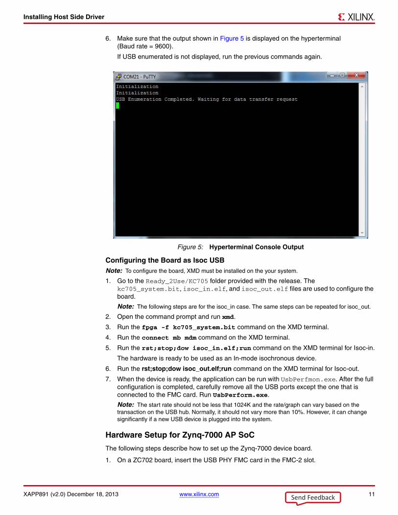
6. Make sure that the output shown in Figure 5 is displayed on the hyperterminal (Baud rate = 9600).
If USB enumerated is not displayed, run the previous commands again.
Configuring the Board as Isoc USBNote: To configure the board, XMD must be installed on the your system.
1. Go to the Ready_2Use/KC705 folder provided with the release. The kc705_system.bit, isoc_in.elf, and isoc_out.elf files are used to configure the board.
Note: The following steps are for the isoc_in case. The same steps can be repeated for isoc_out.
2. Open the command prompt and run xmd.
3. Run the fpga -f kc705_system.bit command on the XMD terminal.
4. Run the connect mb mdm command on the XMD terminal.
5. Run the rst;stop;dow isoc_in.elf;run command on the XMD terminal for Isoc-in.
The hardware is ready to be used as an In-mode isochronous device.
6. Run the rst;stop;dow isoc_out.elf;run command on the XMD terminal for Isoc-out.
7. When the device is ready, the application can be run with UsbPerfmon.exe. After the full configuration is completed, carefully remove all the USB ports except the one that is connected to the FMC card. Run UsbPerform.exe.
Note: The start rate should not be less that 1024K and the rate/graph can vary based on the transaction on the USB hub. Normally, it should not vary more than 10%. However, it can change significantly if a new USB device is plugged into the system.
Hardware Setup for Zynq-7000 AP SoC
The following steps describe how to set up the Zynq-7000 device board.
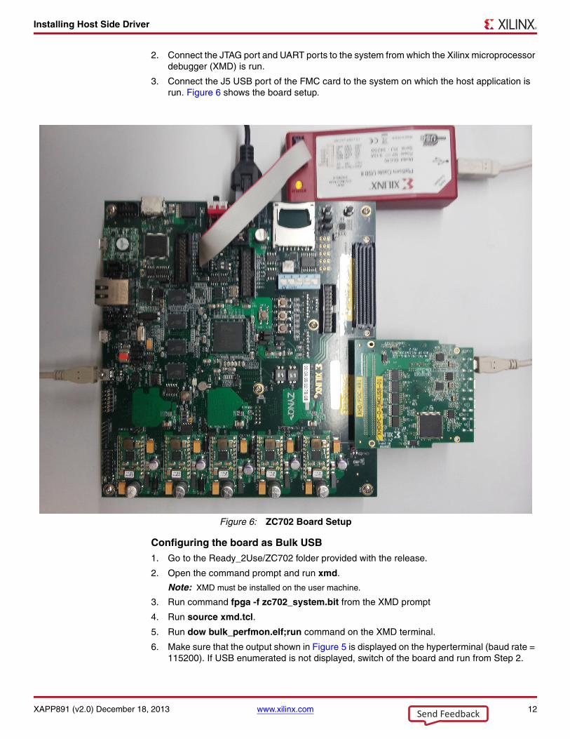
1. On a ZC702 board, insert the USB PHY FMC card in the FMC-2 slot.
X-Ref Target - Figure 5
Figure 5: Hyperterminal Console Output
Send Feedback
Installing Host Side Driver
XAPP891 (v2.0) December 18, 2013 www.xilinx.com 12
2. Connect the JTAG port and UART ports to the system from which the Xilinx microprocessor debugger (XMD) is run.
3. Connect the J5 USB port of the FMC card to the system on which the host application is run. Figure 6 shows the board setup.
Configuring the board as Bulk USB1. Go to the Ready_2Use/ZC702 folder provided with the release.
2. Open the command prompt and run xmd.
Note: XMD must be installed on the user machine.
3. Run command fpga -f zc702_system.bit from the XMD prompt
4. Run source xmd.tcl.
5. Run dow bulk_perfmon.elf;run command on the XMD terminal.
6. Make sure that the output shown in Figure 5 is displayed on the hyperterminal (baud rate = 115200). If USB enumerated is not displayed, switch of the board and run from Step 2.
X-Ref Target - Figure 6
Figure 6: ZC702 Board Setup
Send Feedback
Installing Host Side Driver
XAPP891 (v2.0) December 18, 2013 www.xilinx.com 13
Configuring the Board as Isoc USBNote: To configure the board, XMD must be installed on the your system.
1. Go to the Ready_2Use/ZC702 folder provided with the release. The zc702_system.bit, isoc_in.elf, and isoc_out.elf files are used to configure the board.
Note: The following steps are for the isoc_in case. The same steps can be repeated for isoc_out.
2. Open the command prompt and run xmd.
3. Run command fpga -f zc702_system.bit from XMD prompt.
4. Run source xmd.tcl.
5. Run dow isoc_in.elf;run command on the XMD terminal.
When the device is ready, the application can be run with UsbPerfmon.exe. After the full configuration is completed, carefully remove all the USB ports except the one that is connected to the FMC card. Run UsbPerform.exe.
Note: The start rate should not be less that 1024K and the rate/graph can vary based on the load on the USB hub. Normally, it should not vary more than 10%. However, it can change significantly if a new USB device is plugged into the system.
Send Feedback
Results and Conclusion
XAPP891 (v2.0) December 18, 2013 www.xilinx.com 14
Results and Conclusion
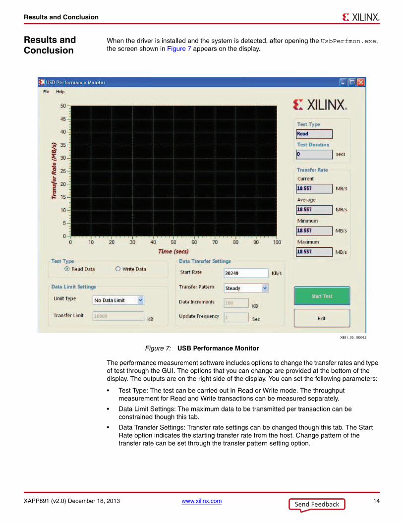
When the driver is installed and the system is detected, after opening the UsbPerfmon.exe, the screen shown in Figure 7 appears on the display.
The performance measurement software includes options to change the transfer rates and type of test through the GUI. The options that you can change are provided at the bottom of the display. The outputs are on the right side of the display. You can set the following parameters:
• Test Type: The test can be carried out in Read or Write mode. The throughput measurement for Read and Write transactions can be measured separately.
• Data Limit Settings: The maximum data to be transmitted per transaction can be constrained though this tab.
• Data Transfer Settings: Transfer rate settings can be changed though this tab. The Start Rate option indicates the starting transfer rate from the host. Change pattern of the transfer rate can be set through the transfer pattern setting option.
X-Ref Target - Figure 7
Figure 7: USB Performance Monitor
X891_09_100912
Send Feedback
Results and Conclusion
XAPP891 (v2.0) December 18, 2013 www.xilinx.com 15
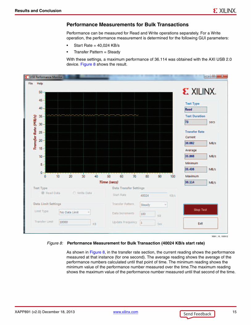
Performance Measurements for Bulk Transactions
Performance can be measured for Read and Write operations separately. For a Write operation, the performance measurement is determined for the following GUI parameters:
• Start Rate = 40,024 KB/s
• Transfer Pattern = Steady
With these settings, a maximum performance of 36.114 was obtained with the AXI USB 2.0 device. Figure 8 shows the result.
As shown in Figure 8, in the transfer rate section, the current reading shows the performance measured at that instance (for one second). The average reading shows the average of the performance numbers calculated until that point of time. The minimum reading shows the minimum value of the performance number measured over the time.The maximum reading shows the maximum value of the performance number measured until that second of the time.
X-Ref Target - Figure 8
Figure 8: Performance Measurement for Bulk Transaction (40024 KB/s start rate)
X891_10_100912
Send Feedback
Results and Conclusion
XAPP891 (v2.0) December 18, 2013 www.xilinx.com 16
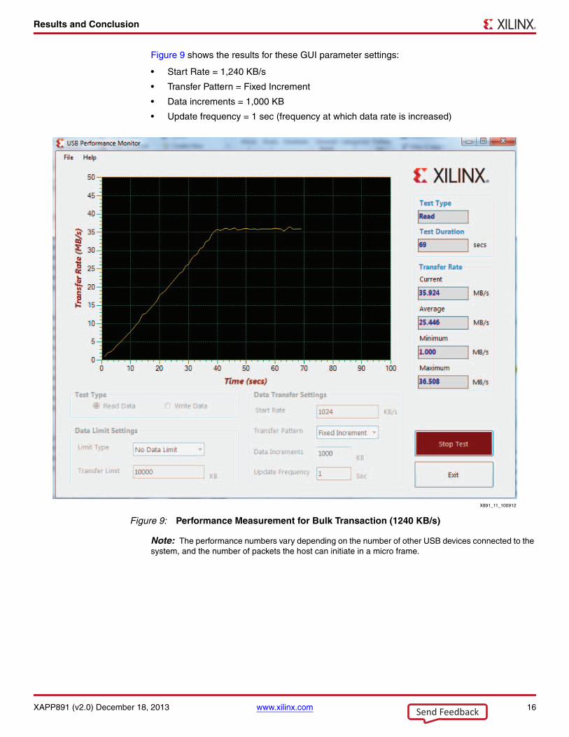
Figure 9 shows the results for these GUI parameter settings:
• Start Rate = 1,240 KB/s
• Transfer Pattern = Fixed Increment
• Data increments = 1,000 KB
• Update frequency = 1 sec (frequency at which data rate is increased)
Note: The performance numbers vary depending on the number of other USB devices connected to the system, and the number of packets the host can initiate in a micro frame.
X-Ref Target - Figure 9
Figure 9: Performance Measurement for Bulk Transaction (1240 KB/s)
X891_11_100912
Send Feedback
Results and Conclusion
XAPP891 (v2.0) December 18, 2013 www.xilinx.com 17
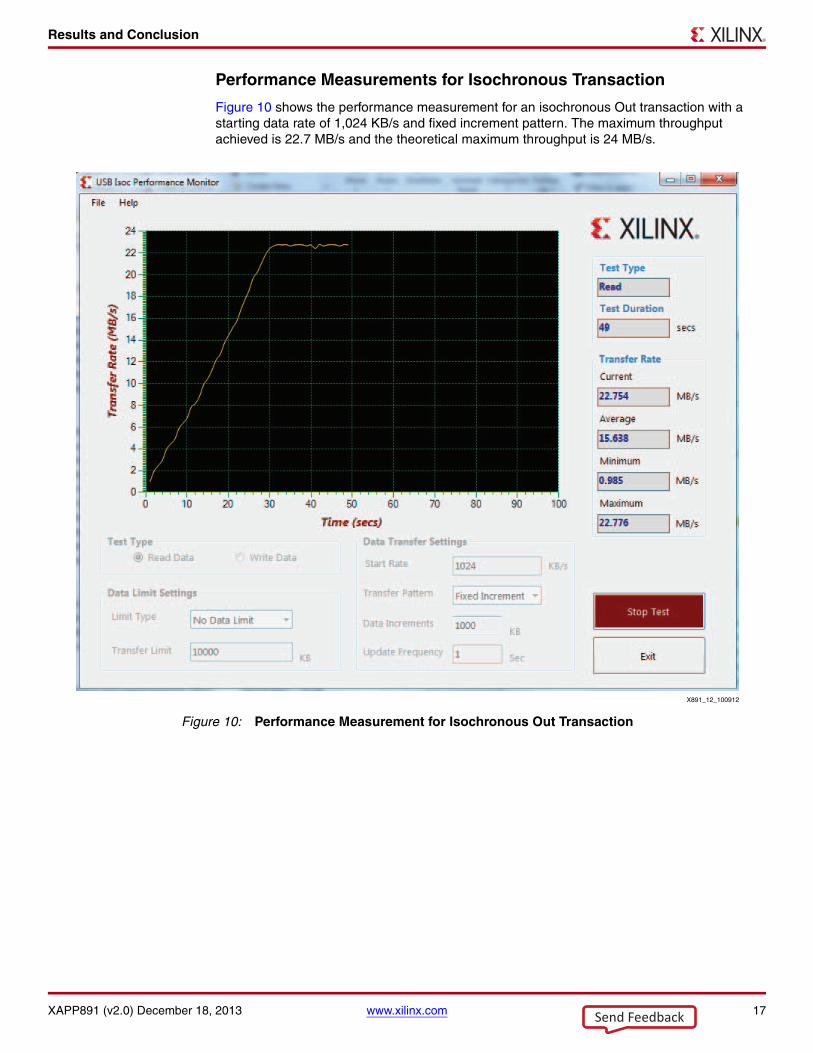
Performance Measurements for Isochronous Transaction
Figure 10 shows the performance measurement for an isochronous Out transaction with a starting data rate of 1,024 KB/s and fixed increment pattern. The maximum throughput achieved is 22.7 MB/s and the theoretical maximum throughput is 24 MB/s.
X-Ref Target - Figure 10
Figure 10: Performance Measurement for Isochronous Out Transaction
X891_12_100912
Send Feedback
Results and Conclusion
XAPP891 (v2.0) December 18, 2013 www.xilinx.com 18
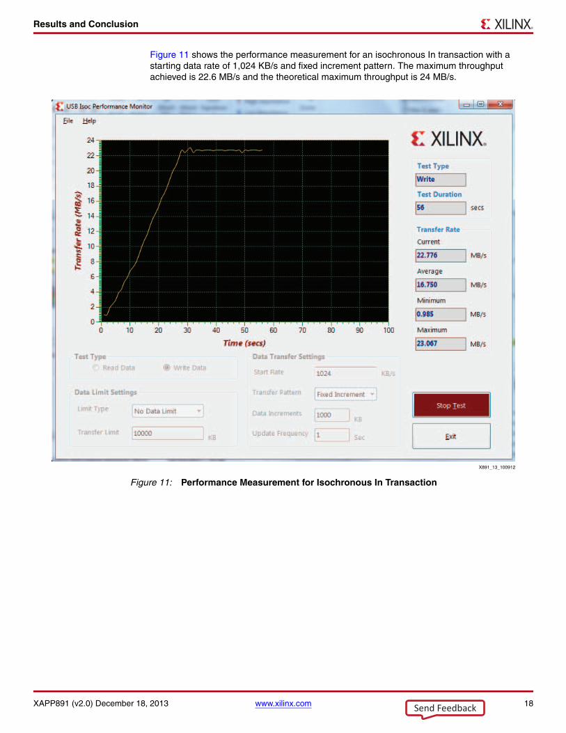
Figure 11 shows the performance measurement for an isochronous In transaction with a starting data rate of 1,024 KB/s and fixed increment pattern. The maximum throughput achieved is 22.6 MB/s and the theoretical maximum throughput is 24 MB/s.
X-Ref Target - Figure 11
Figure 11: Performance Measurement for Isochronous In Transaction
X891_13_100912
Send Feedback
Reference Design Parameters
XAPP891 (v2.0) December 18, 2013 www.xilinx.com 19
Reference Design Parameters
The reference design files for this application note can be downloaded from:
//secure.xilinx.com/webreg/clickthrough.do?cid=199301
Table 4 lists the reference design parameters.
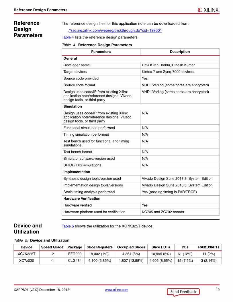
Device and Utilization
Table 5 shows the utilization for the XC7K325T device.
Table 4: Reference Design Parameters
Parameters Description
General
Developer name Ravi Kiran Boddu, Dinesh Kumar
Target devices Kintex-7 and Zynq-7000 devices
Source code provided Yes
Source code format VHDL/Verilog (some cores are encrypted)
Design uses code/IP from existing Xilinx application note/reference designs, Vivado design tools, or third party
VHDL/Verilog (some cores are encrypted)
Simulation
Design uses code/IP from existing Xilinx application note/reference designs, Vivado design tools, or third party
N/A
Functional simulation performed N/A
Timing simulation performed N/A
Test bench used for functional and timing simulations
N/A
Test bench format N/A
Simulator software/version used N/A
SPICE/IBIS simulations N/A
Implementation
Synthesis design tools/version used Vivado Design Suite 2013.3: System Edition
Implementation design tools/versions Vivado Design Suite 2013.3: System Edition
Static timing analysis performed Yes (passing timing in PAR/TRCE)
Hardware Verification
Hardware verified Yes
Hardware platform used for verification KC705 and ZC702 boards
Table 5: Device and Utilization
Device Speed Grade Package Slice Registers Occupied Slices Slice LUTs I/Os RAMB36E1s
XC7K325T -2 FFG900 8,002 (1%) 4,364 (8%) 10,995 (5%) 61 (12%) 11 (2%)
XC7z020 -1 CLG484 4,100 (3.85%) 1,807 (13.58%) 4,606 (8.65%) 15 (7.5%) 3 (2.14%)
Send Feedback
References
XAPP891 (v2.0) December 18, 2013 www.xilinx.com 20
References This section lists the references used in this document.
1. LogiCORE IP AXI Universal Serial Bus (USB) 2.0 Device v5.0 Product Guide (PG137)
2. Vivado Design Suite User Guide: Designing IP Subsystems using IP Integrator (UG994)
Revision History
The following table shows the revision history for this document.
Notice of Disclaimer
The information disclosed to you hereunder (the “Materials”) is provided solely for the selection and use ofXilinx products. To the maximum extent permitted by applicable law: (1) Materials are made available "ASIS" and with all faults, Xilinx hereby DISCLAIMS ALL WARRANTIES AND CONDITIONS, EXPRESS,IMPLIED, OR STATUTORY, INCLUDING BUT NOT LIMITED TO WARRANTIES OFMERCHANTABILITY, NON-INFRINGEMENT, OR FITNESS FOR ANY PARTICULAR PURPOSE; and (2)Xilinx shall not be liable (whether in contract or tort, including negligence, or under any other theory ofliability) for any loss or damage of any kind or nature related to, arising under, or in connection with, theMaterials (including your use of the Materials), including for any direct, indirect, special, incidental, orconsequential loss or damage (including loss of data, profits, goodwill, or any type of loss or damagesuffered as a result of any action brought by a third party) even if such damage or loss was reasonablyforeseeable or Xilinx had been advised of the possibility of the same. Xilinx assumes no obligation tocorrect any errors contained in the Materials or to notify you of updates to the Materials or to productspecifications. You may not reproduce, modify, distribute, or publicly display the Materials without priorwritten consent. Certain products are subject to the terms and conditions of the Limited Warranties whichcan be viewed at http://www.xilinx.com/warranty.htm; IP cores may be subject to warranty and supportterms contained in a license issued to you by Xilinx. Xilinx products are not designed or intended to befail-safe or for use in any application requiring fail-safe performance; you assume sole risk and liability foruse of Xilinx products in Critical Applications: http://www.xilinx.com/warranty.htm#critapps.
Automotive Applications DisclaimerXILINX PRODUCTS ARE NOT DESIGNED OR INTENDED TO BE FAIL-SAFE, OR FOR USE IN ANYAPPLICATION REQUIRING FAIL-SAFE PERFORMANCE, SUCH AS APPLICATIONS RELATED TO: (I)THE DEPLOYMENT OF AIRBAGS, (II) CONTROL OF A VEHICLE, UNLESS THERE IS A FAIL-SAFEOR REDUNDANCY FEATURE (WHICH DOES NOT INCLUDE USE OF SOFTWARE IN THE XILINXDEVICE TO IMPLEMENT THE REDUNDANCY) AND A WARNING SIGNAL UPON FAILURE TO THEOPERATOR, OR (III) USES THAT COULD LEAD TO DEATH OR PERSONAL INJURY. CUSTOMERASSUMES THE SOLE RISK AND LIABILITY OF ANY USE OF XILINX PRODUCTS IN SUCHAPPLICATIONS.
Date Version Description of Revisions
12/19/2012 1.0 Initial Xilinx release.
02/14/2013 1.0.1 Minor typographical edits. Updated PDF properties.
12/18/2013 2.0 Updated for Vivado IP Integrator design.Added Zynq-7000 AP SoC support.
Send Feedback