Embed Size (px)
Citation preview
1
XMUT303 Analogue Electronics
Mid-Term Test Revision Questions (Answer)
A. Operational Amplifier
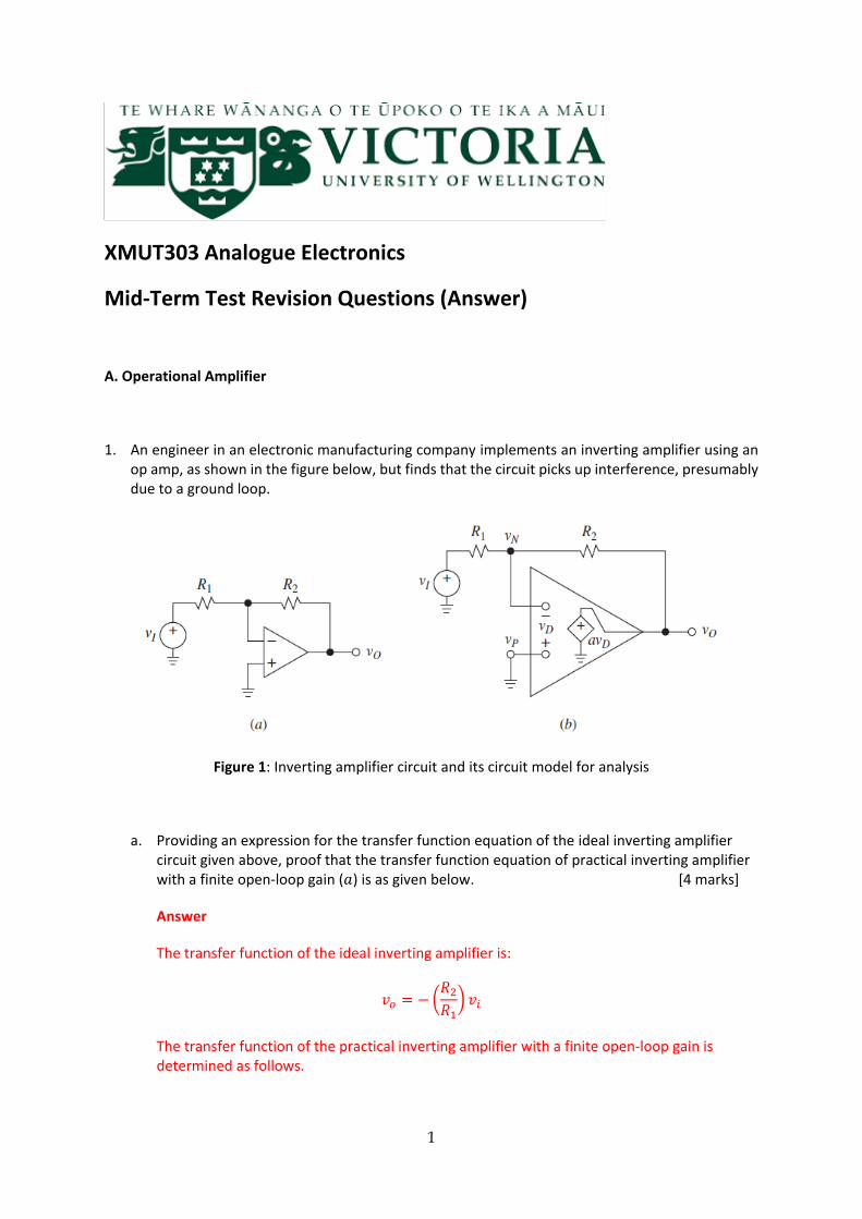
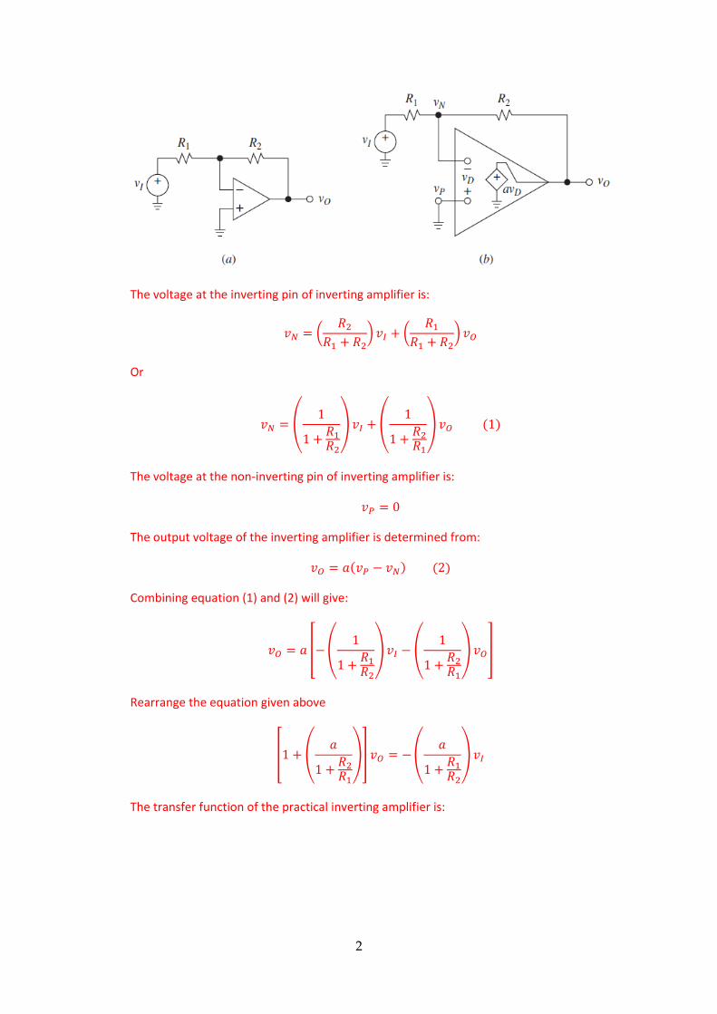
1. An engineer in an electronic manufacturing company implements an inverting amplifier using an op amp, as shown in the figure below, but finds that the circuit picks up interference, presumably due to a ground loop.
Figure 1: Inverting amplifier circuit and its circuit model for analysis
a. Providing an expression for the transfer function equation of the ideal inverting amplifier circuit given above, proof that the transfer function equation of practical inverting amplifier with a finite open-loop gain (𝑎) is as given below. [4 marks]
Answer
The transfer function of the ideal inverting amplifier is:
𝑣𝑜 = − (𝑅2
𝑅1) 𝑣𝑖
The transfer function of the practical inverting amplifier with a finite open-loop gain is determined as follows.
2
The voltage at the inverting pin of inverting amplifier is:
𝑣𝑁 = (𝑅2
𝑅1 + 𝑅2) 𝑣𝐼 + (
𝑅1
𝑅1 + 𝑅2) 𝑣𝑂
Or
𝑣𝑁 = (1
1 +𝑅1𝑅2
) 𝑣𝐼 + (1
1 +𝑅2𝑅1
) 𝑣𝑂 (1)
The voltage at the non-inverting pin of inverting amplifier is:
𝑣𝑃 = 0
The output voltage of the inverting amplifier is determined from:
𝑣𝑂 = 𝑎(𝑣𝑃 − 𝑣𝑁) (2)
Combining equation (1) and (2) will give:
𝑣𝑂 = 𝑎 [− (1
1 +𝑅1𝑅2
) 𝑣𝐼 − (1
1 +𝑅2𝑅1
) 𝑣𝑂]
Rearrange the equation given above
[1 + (𝑎
1 +𝑅2𝑅1
)] 𝑣𝑂 = − (𝑎
1 +𝑅1𝑅2
) 𝑣𝐼
The transfer function of the practical inverting amplifier is:
3
𝑣𝑂
𝑣𝐼=
(𝑎
1 +𝑅1𝑅2
)
1 + (𝑎
1 +𝑅2𝑅1
)
Simplify the equation above becomes:
𝑣𝑂
𝑣𝐼= − (
𝑅2
𝑅1) [
1
1 + (1𝑎
) (𝑅1 + 𝑅2
𝑅1)
]
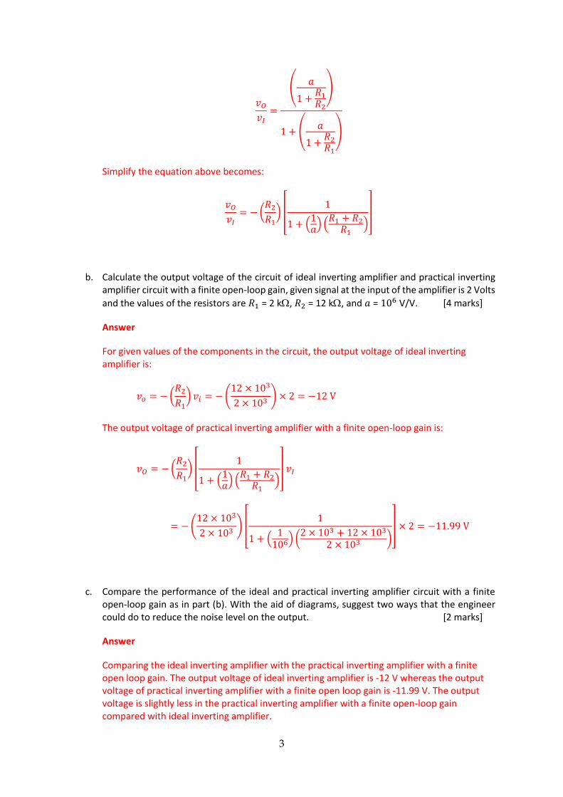
b. Calculate the output voltage of the circuit of ideal inverting amplifier and practical inverting amplifier circuit with a finite open-loop gain, given signal at the input of the amplifier is 2 Volts
and the values of the resistors are 𝑅1 = 2 k, 𝑅2 = 12 k, and 𝑎 = 106 V/V. [4 marks]
Answer
For given values of the components in the circuit, the output voltage of ideal inverting amplifier is:
𝑣𝑜 = − (𝑅2
𝑅1) 𝑣𝑖 = − (
12 × 103
2 × 103) × 2 = −12 V
The output voltage of practical inverting amplifier with a finite open-loop gain is:
𝑣𝑂 = − (𝑅2
𝑅1) [
1
1 + (1𝑎
) (𝑅1 + 𝑅2
𝑅1)
] 𝑣𝐼
= − (12 × 103
2 × 10³) [
1
1 + (1
106) (2 × 10³ + 12 × 103
2 × 10³ )] × 2 = −11.99 V
c. Compare the performance of the ideal and practical inverting amplifier circuit with a finite open-loop gain as in part (b). With the aid of diagrams, suggest two ways that the engineer could do to reduce the noise level on the output. [2 marks]
Answer
Comparing the ideal inverting amplifier with the practical inverting amplifier with a finite open loop gain. The output voltage of ideal inverting amplifier is -12 V whereas the output voltage of practical inverting amplifier with a finite open loop gain is -11.99 V. The output voltage is slightly less in the practical inverting amplifier with a finite open-loop gain compared with ideal inverting amplifier.
4
The solution to reduce the noise level at the output of the amplifier could be by e.g. using differential input amplifier, using twisted pair cable, or adding ferrite-bead choke.
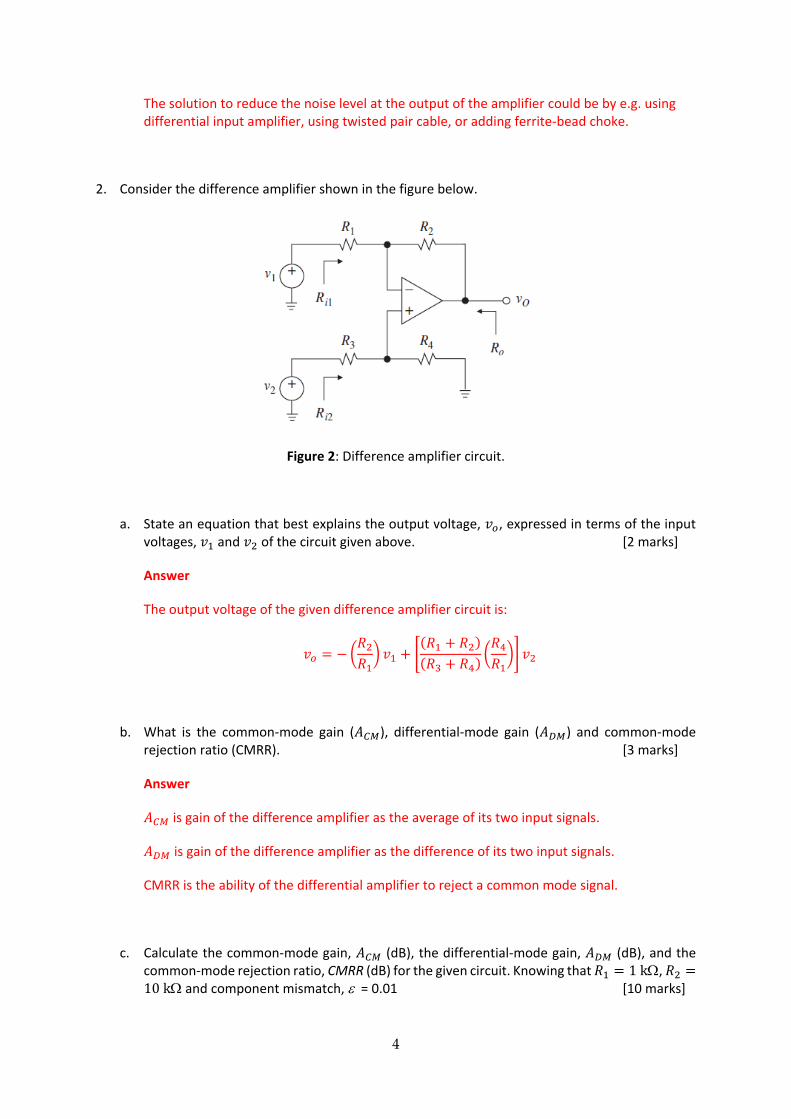
2. Consider the difference amplifier shown in the figure below.
Figure 2: Difference amplifier circuit.
a. State an equation that best explains the output voltage, 𝑣𝑜, expressed in terms of the input voltages, 𝑣1 and 𝑣2 of the circuit given above. [2 marks]
Answer
The output voltage of the given difference amplifier circuit is:
𝑣𝑜 = − (𝑅2
𝑅1) 𝑣1 + [
(𝑅1 + 𝑅2)
(𝑅3 + 𝑅4)(
𝑅4
𝑅1)] 𝑣2
b. What is the common-mode gain (𝐴𝐶𝑀), differential-mode gain (𝐴𝐷𝑀) and common-mode rejection ratio (CMRR). [3 marks]
Answer
𝐴𝐶𝑀 is gain of the difference amplifier as the average of its two input signals.
𝐴𝐷𝑀 is gain of the difference amplifier as the difference of its two input signals.
CMRR is the ability of the differential amplifier to reject a common mode signal.
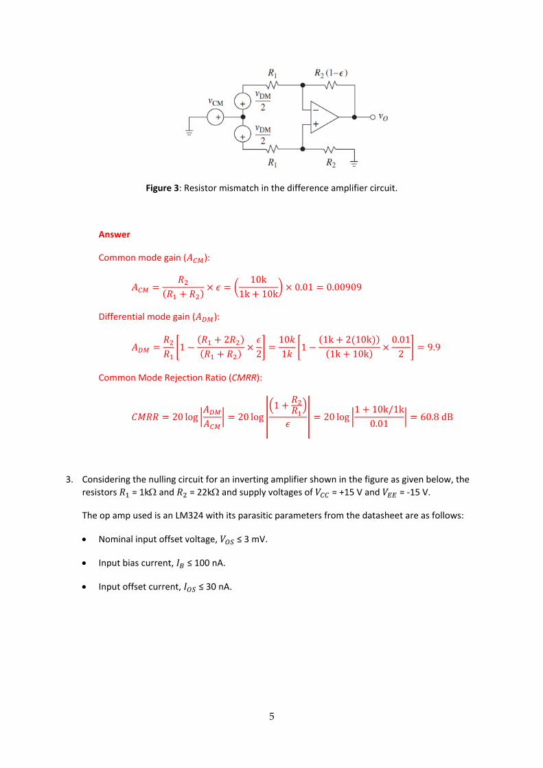
c. Calculate the common-mode gain, 𝐴𝐶𝑀 (dB), the differential-mode gain, 𝐴𝐷𝑀 (dB), and the common-mode rejection ratio, CMRR (dB) for the given circuit. Knowing that 𝑅1 = 1 k, 𝑅2 =10 k and component mismatch, = 0.01 [10 marks]
5
Figure 3: Resistor mismatch in the difference amplifier circuit.
Answer
Common mode gain (𝐴𝐶𝑀):
𝐴𝐶𝑀 =𝑅2
(𝑅1 + 𝑅2)× 𝜖 = (
10k
1k + 10k) × 0.01 = 0.00909
Differential mode gain (𝐴𝐷𝑀):
𝐴𝐷𝑀 =𝑅2
𝑅1[1 −
(𝑅1 + 2𝑅2)
(𝑅1 + 𝑅2)×
𝜖
2] =
10𝑘
1𝑘[1 −
(1k + 2(10k))
(1k + 10k)×
0.01
2] = 9.9
Common Mode Rejection Ratio (CMRR):
𝐶𝑀𝑅𝑅 = 20 log |𝐴𝐷𝑀
𝐴𝐶𝑀| = 20 log |
(1 +𝑅2𝑅1
)
𝜖| = 20 log |
1 + 10k/1k
0.01| = 60.8 dB
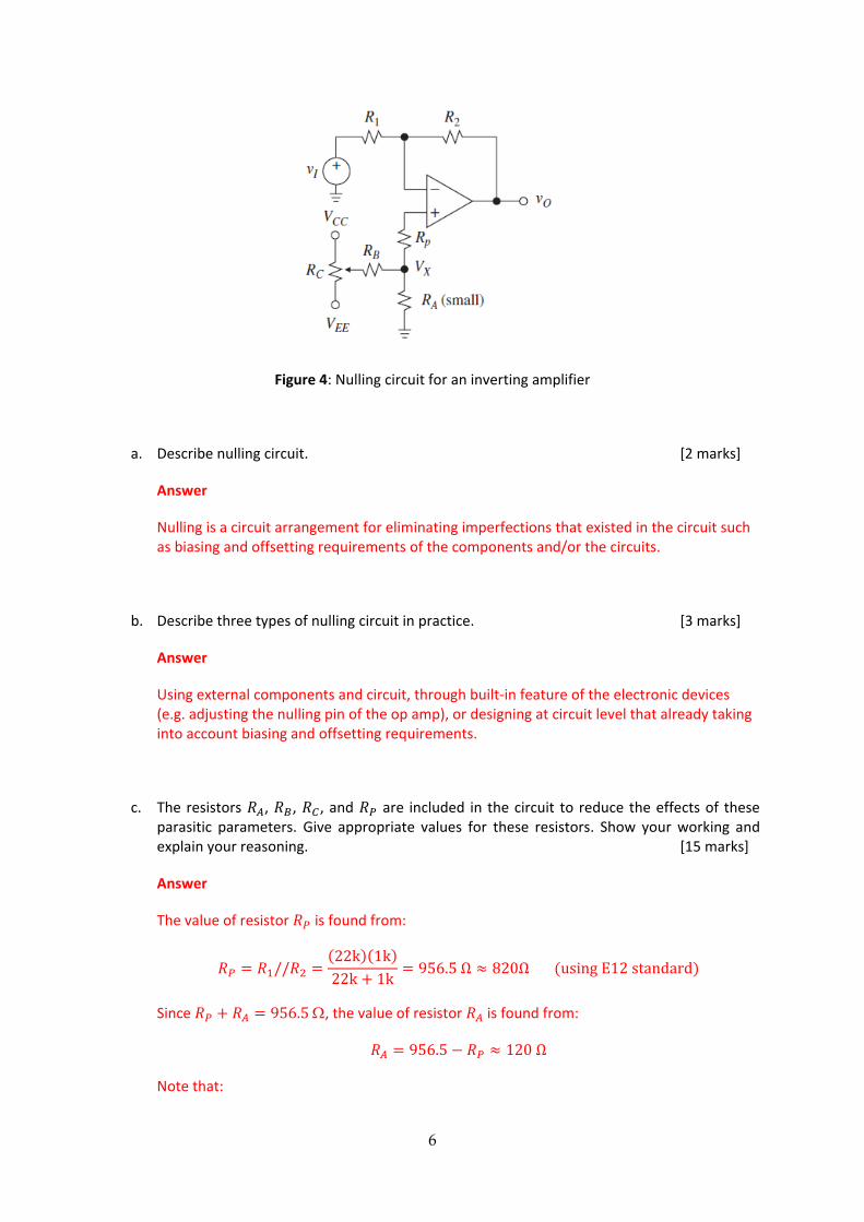
3. Considering the nulling circuit for an inverting amplifier shown in the figure as given below, the
resistors 𝑅1 = 1k and 𝑅2 = 22k and supply voltages of 𝑉𝐶𝐶 = +15 V and 𝑉𝐸𝐸 = -15 V.
The op amp used is an LM324 with its parasitic parameters from the datasheet are as follows:
Nominal input offset voltage, 𝑉𝑂𝑆 ≤ 3 mV.
Input bias current, 𝐼𝐵 ≤ 100 nA.
Input offset current, 𝐼𝑂𝑆 ≤ 30 nA.
6
Figure 4: Nulling circuit for an inverting amplifier
a. Describe nulling circuit. [2 marks]
Answer
Nulling is a circuit arrangement for eliminating imperfections that existed in the circuit such as biasing and offsetting requirements of the components and/or the circuits.
b. Describe three types of nulling circuit in practice. [3 marks]
Answer
Using external components and circuit, through built-in feature of the electronic devices (e.g. adjusting the nulling pin of the op amp), or designing at circuit level that already taking into account biasing and offsetting requirements.
c. The resistors 𝑅𝐴, 𝑅𝐵, 𝑅𝐶, and 𝑅𝑃 are included in the circuit to reduce the effects of these parasitic parameters. Give appropriate values for these resistors. Show your working and explain your reasoning. [15 marks]
Answer
The value of resistor 𝑅𝑃 is found from:
𝑅𝑃 = 𝑅1//𝑅2 =(22k)(1k)
22k + 1k= 956.5 Ω ≈ 820Ω (using E12 standard)
Since 𝑅𝑃 + 𝑅𝐴 = 956.5 , the value of resistor 𝑅𝐴 is found from:
𝑅𝐴 = 956.5 − 𝑅𝑃 ≈ 120 Ω
Note that:
7
𝑅𝑃 + 𝑅𝐴 > 𝑅1//𝑅2
But, the value of 𝑉𝑛𝑢𝑙𝑙 is found from:
𝑉𝑛𝑢𝑙𝑙 = 𝑉𝑂𝑆 + 𝐼𝑂𝑆 × (𝑅𝑃 + 𝑅𝐴)
= 3 mV + 30 nA × (820 + 120) = 3.03 mV
Say that we use 5 mV to be safe.
±𝑉𝑛𝑢𝑙𝑙
±𝑉𝐶𝐶=
𝑅𝐴
𝑅𝐴 + 𝑅𝐵≈
𝑅𝐴
𝑅𝐵
Rearranging and entering values into the equation, the value of resistor 𝑅𝐵 is:
𝑅𝐵 = (±𝑉𝐶𝐶
±𝑉𝑛𝑢𝑙𝑙) 𝑅𝐴
= (±15 V
±5 mV) × 120Ω = 360 kΩ
Then the value of resistor 𝑅𝐶 is found from (note that 𝑅𝐶 is a variable resistor):
𝑅𝐶 =𝑅𝐵
10≈ 10 − 50 kΩ
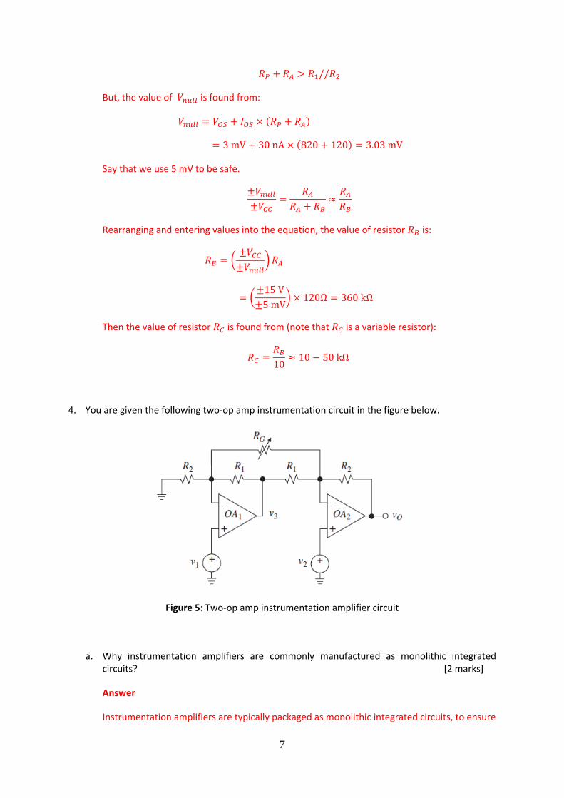
4. You are given the following two-op amp instrumentation circuit in the figure below.
Figure 5: Two-op amp instrumentation amplifier circuit
a. Why instrumentation amplifiers are commonly manufactured as monolithic integrated circuits? [2 marks]
Answer
Instrumentation amplifiers are typically packaged as monolithic integrated circuits, to ensure
8
that they have high common mode rejection ratio.
b. If you have to design an op amp based amplifier in cascading arrangement, what circuit feature usually you have at the output stage? Give two reasons for your answer. [2 marks]
Answer
The output stage of a multistage amplifier usually employs a push-pull amplifier. It is to ensure sufficient coverage of the signal bandwidth and adequate driving of the load.
c. State an expression for the gain, 𝑣𝑜
𝑣2−𝑣1, for the circuit shown in the circuit above.
[3 marks] Answer
The expression for the gain of the given instrumentation amplifier circuit is:
𝑣𝑜
𝑣2 − 𝑣1= 1 +
𝑅2
𝑅1+ 2
𝑅2
𝑅𝐺
d. Calculate the minimum gain of the circuit shown above if 𝑅1 = 1 k and 𝑅2 = 10 k. [4 marks]
Answer
Providing Rg is typically considerably bigger than R2, the minimum gain of the instrumentation amplifier circuit is 11 times.
Gain(min) ≈ 1 +𝑅2
𝑅1= 1 +
10k
1k= 11
B. Op Amp Analysis
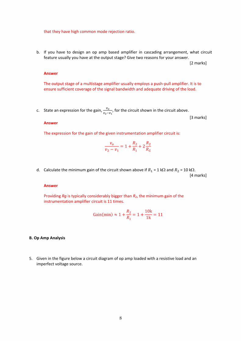
5. Given in the figure below a circuit diagram of op amp loaded with a resistive load and an imperfect voltage source.
9
Figure 6: circuit diagram of loading of an op amp
a. Describe the difference between op amp with FET input stages with those with BJT transistors. [2 marks]
Answer
Compared to op amps with FET input stages, op amps with BJT input stages have higher bias current but lower offset voltage.
b. The amplifier above has 𝑅𝑖 = 100k , 𝐴𝑜𝑐 = 100 V/V, and 𝑅𝑜 = 1 and is driven by a source
with 𝑅𝑠 = 25k and drives a load 𝑅𝑙 = 3 . Calculate the overall gain as well as the amount of input and output loading. [10 marks]
Answer
By using the equation given in (a), we obtain the overall gain of the amplifier:
𝑉𝑂
𝑉𝑆=
𝑅𝑖
𝑅𝑠 + 𝑅𝑖𝐴𝑜𝑐
𝑅𝑙
𝑅𝑜 + 𝑅𝑙
As a result, the overall gain for the first case is
𝑉𝑂
𝑉𝑆= (
100k
25k + 100k) × 100 × (
3
1 + 3)
= 0.8 × 100 × 0.75 = 60
This is less than 100 V/V because of loading.
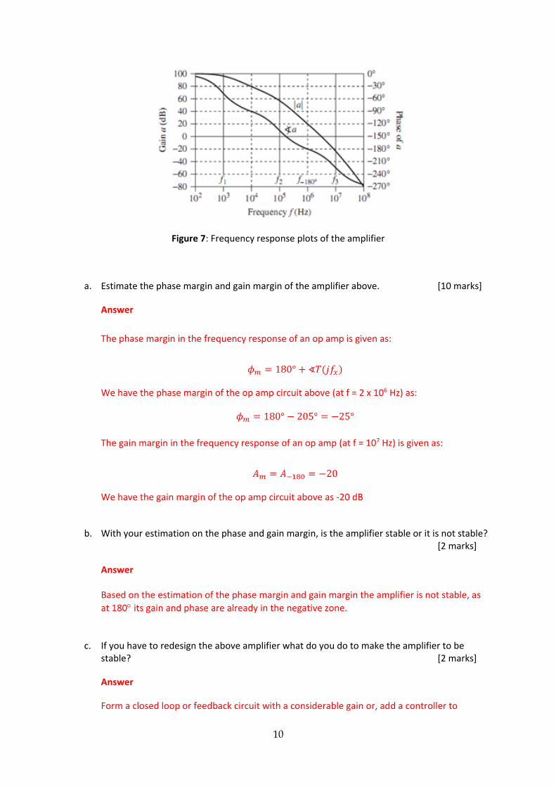
6. Given in the figure below is a frequency response of an open loop voltage amplifier.
10
Figure 7: Frequency response plots of the amplifier
a. Estimate the phase margin and gain margin of the amplifier above. [10 marks]
Answer
The phase margin in the frequency response of an op amp is given as:
𝜙𝑚 = 180° + ∢𝑇(𝑗𝑓𝑥)
We have the phase margin of the op amp circuit above (at f = 2 x 10⁶ Hz) as:
𝜙𝑚 = 180° − 205° = −25°
The gain margin in the frequency response of an op amp (at f = 107 Hz) is given as:
𝐴𝑚 = 𝐴−180 = −20
We have the gain margin of the op amp circuit above as -20 dB
b. With your estimation on the phase and gain margin, is the amplifier stable or it is not stable?
[2 marks]
Answer Based on the estimation of the phase margin and gain margin the amplifier is not stable, as
at 180 its gain and phase are already in the negative zone.
c. If you have to redesign the above amplifier what do you do to make the amplifier to be
stable? [2 marks]
Answer
Form a closed loop or feedback circuit with a considerable gain or, add a controller to
11
compensate for introducing extra gain or phase margins to the amplifier.
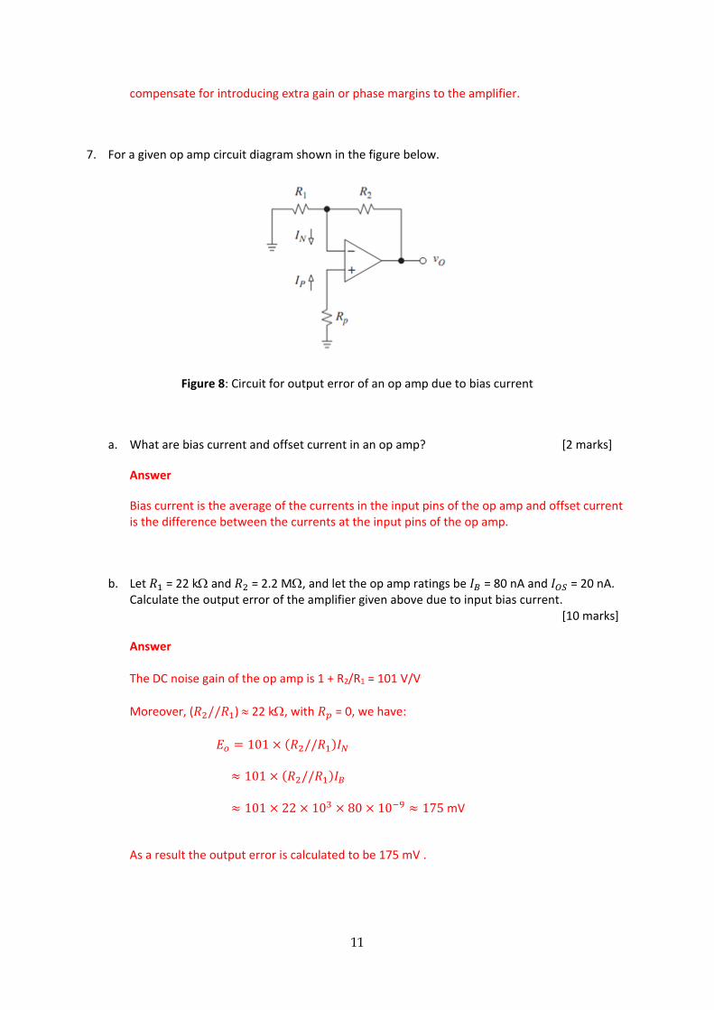
7. For a given op amp circuit diagram shown in the figure below.
Figure 8: Circuit for output error of an op amp due to bias current
a. What are bias current and offset current in an op amp? [2 marks]
Answer
Bias current is the average of the currents in the input pins of the op amp and offset current is the difference between the currents at the input pins of the op amp.
b. Let 𝑅1 = 22 k and 𝑅2 = 2.2 M, and let the op amp ratings be 𝐼𝐵 = 80 nA and 𝐼𝑂𝑆 = 20 nA. Calculate the output error of the amplifier given above due to input bias current. [10 marks]
Answer The DC noise gain of the op amp is 1 + R2/R1 = 101 V/V
Moreover, (𝑅2//𝑅1) 22 k, with 𝑅𝑝 = 0, we have:
𝐸𝑜 = 101 × (𝑅2//𝑅1)𝐼𝑁
≈ 101 × (𝑅2//𝑅1)𝐼𝐵
≈ 101 × 22 × 103 × 80 × 10−9 ≈ 175 mV
As a result the output error is calculated to be 175 mV .
12
C. Op Amp based Circuits I
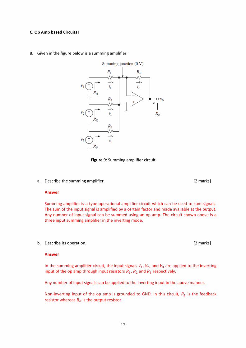
8. Given in the figure below is a summing amplifier.
Figure 9: Summing amplifier circuit
a. Describe the summing amplifier. [2 marks]
Answer
Summing amplifier is a type operational amplifier circuit which can be used to sum signals. The sum of the input signal is amplified by a certain factor and made available at the output. Any number of input signal can be summed using an op amp. The circuit shown above is a three input summing amplifier in the inverting mode.
b. Describe its operation. [2 marks]
Answer
In the summing amplifier circuit, the input signals 𝑉1, 𝑉2, and 𝑉3 are applied to the inverting input of the op amp through input resistors 𝑅1, 𝑅2 and 𝑅3 respectively.
Any number of input signals can be applied to the inverting input in the above manner.
Non-inverting input of the op amp is grounded to GND. In this circuit, 𝑅𝑓 is the feedback
resistor whereas 𝑅𝑜 is the output resistor.
13
c. Derive its transfer function. [8 marks]
Answer
By applying Kirchhoff’s current law at summing junction node we get:
𝐼1 + 𝐼2 + 𝐼3 = 𝐼𝑓 + 𝐼𝑝𝑖𝑛−
Since the input resistance of an ideal op amp is close to infinity and has infinite gain. We can neglect the current that flows to the inverting pin of the op amp (𝐼𝑝𝑖𝑛−) & voltage at the
summing junction (𝑉𝑠), therefore:
𝐼1 + 𝐼2 + 𝐼3 = 𝐼𝑓 (1)
Equation (1) can be rewritten as:
(𝑉1
𝑅1) + (
𝑉2
𝑅2) + (
𝑉3
𝑅3) =
𝑉𝑠 − 𝑉𝑜
𝑅𝑓
Neglecting 𝑉𝑠, we get:
(𝑉1
𝑅1) + (
𝑉2
𝑅2) + (
𝑉3
𝑅3) = −
𝑉𝑜
𝑅𝑓
Rearrange the equation:
𝑉𝑜 = −𝑅𝑓 [(𝑉1
𝑅1) + (
𝑉2
𝑅2) + (
𝑉3
𝑅3)]
Also,
𝑉𝑜 = − [(𝑅𝑓
𝑅1) 𝑉1 + (
𝑅𝑓
𝑅2) 𝑉2 + (
𝑅𝑓
𝑅3) 𝑉3] (2)
If resistor 𝑅1, 𝑅2 and 𝑅3 has same value i.e. 𝑅1 = 𝑅2 = 𝑅3 = 𝑅, then equation (2) can be written as:
𝑉𝑜 = − (𝑅𝑓
𝑅) (𝑉1 + 𝑉2 + 𝑉3) (3)
If the values of 𝑅𝑓 and 𝑅 are made equal, then the equation becomes:
𝑉𝑜 = −(𝑉1 + 𝑉2 + 𝑉3)
d. Describe two applications of summing amplifier. [4 marks]
Answer
14
Two applications of summing amplifier are: averaging circuit and scaling amplifier.
Averaging Circuit :
An averaging circuit can be made from the summing amplifier circuit by making the all input resistor equal in value i.e.
𝑅1 = 𝑅2 = 𝑅3 = 𝑅
and the gain must be selected such that if there are m inputs, then
𝑅𝑓
𝑅 =
1
𝑚
Scaling amplifier :
In a scaling amplifier each input will be multiplied by a different factor and then summed together.
Scaling amplifier is also called a weighted amplifier.
In this case different values are chosen for 𝑅1, 𝑅2 and 𝑅3. The governing equation is:
𝑉𝑜 = − [(𝑅𝑓
𝑅1) 𝑉1 + (
𝑅𝑓
𝑅2) 𝑉2 + (
𝑅𝑓
𝑅3) 𝑉3]
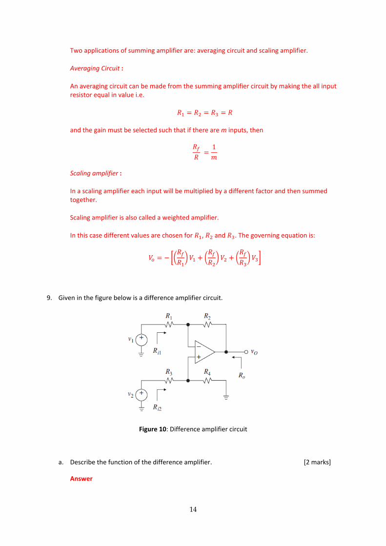
9. Given in the figure below is a difference amplifier circuit.
Figure 10: Difference amplifier circuit
a. Describe the function of the difference amplifier. [2 marks]
Answer
15
Differential amplifiers amplify the difference between two voltages making this type of operational amplifier circuit a subtractor unlike a summing amplifier which adds or sums together the input voltages.
b. Derive its transfer function equation. [8 marks]
Answer By connecting each input in turn to 0 V ground we can use superposition to solve for the output voltage 𝑉𝑜𝑢𝑡. Then the transfer function for a differential amplifier circuit is given as:
𝐼1 =𝑉1 − 𝑉𝑎
𝑅1 𝐼2 =
𝑉2 − 𝑉𝑏
𝑅2 𝐼𝑓 =
𝑉𝑎 − 𝑉𝑜𝑢𝑡
𝑅3
At summing point, 𝑉𝑎 = 𝑉𝑏 and
𝑉𝑏 = 𝑉2 (𝑅4
𝑅2 + 𝑅4)
If 𝑉2 = 0, then
𝑉𝑜𝑢𝑡(𝑎) = −𝑉1 (𝑅3
𝑅1)
If 𝑉1 = 0, then
𝑉𝑜𝑢𝑡(𝑏) = 𝑉2 (𝑅4
𝑅2 + 𝑅4) (
𝑅1 + 𝑅3
𝑅1)
But,
𝑉𝑜𝑢𝑡 = −𝑉𝑜𝑢𝑡(𝑎) + 𝑉𝑜𝑢𝑡(𝑏)
Finally
𝑉𝑜𝑢𝑡 = −𝑉1 (𝑅3
𝑅1) + 𝑉2 (
𝑅4
𝑅2 + 𝑅4) (
𝑅1 + 𝑅3
𝑅1)
When resistors, 𝑅1 = 𝑅2 and 𝑅3 = 𝑅4 the above transfer function for the differential amplifier can be simplified to the following expression:
𝑉𝑜𝑢𝑡 =𝑅3
𝑅1
(𝑉2 − 𝑉1)
c. Describe two of its application in practice. [4 marks]
Answer Two applications of the difference amplifier in practice: Wheatstone bridge differential amplifier and light activated differential amplifier. Wheatstone Bridge Differential Amplifier

16
The standard Differential Amplifier circuit now becomes a differential voltage comparator by “comparing” one input voltage to the other. By connecting one input to a fixed voltage reference set up on one leg of the resistive bridge network and the other to either a “Thermistor” or a “Light Dependant Resistor”, the amplifier circuit can be used to detect either low or high levels of temperature or light. In this case the output voltage becomes a linear function of the changes in the active leg of the resistive bridge.
Light Activated Differential Amplifier
The circuit above acts as a light-activated switch which turns the output relay either “ON” or “OFF” as the light level detected by the LDR resistor exceeds or falls below some pre-set value. A fixed voltage reference is applied to the non-inverting input terminal of the op-amp via the 𝑅1 − 𝑅2 voltage divider network.
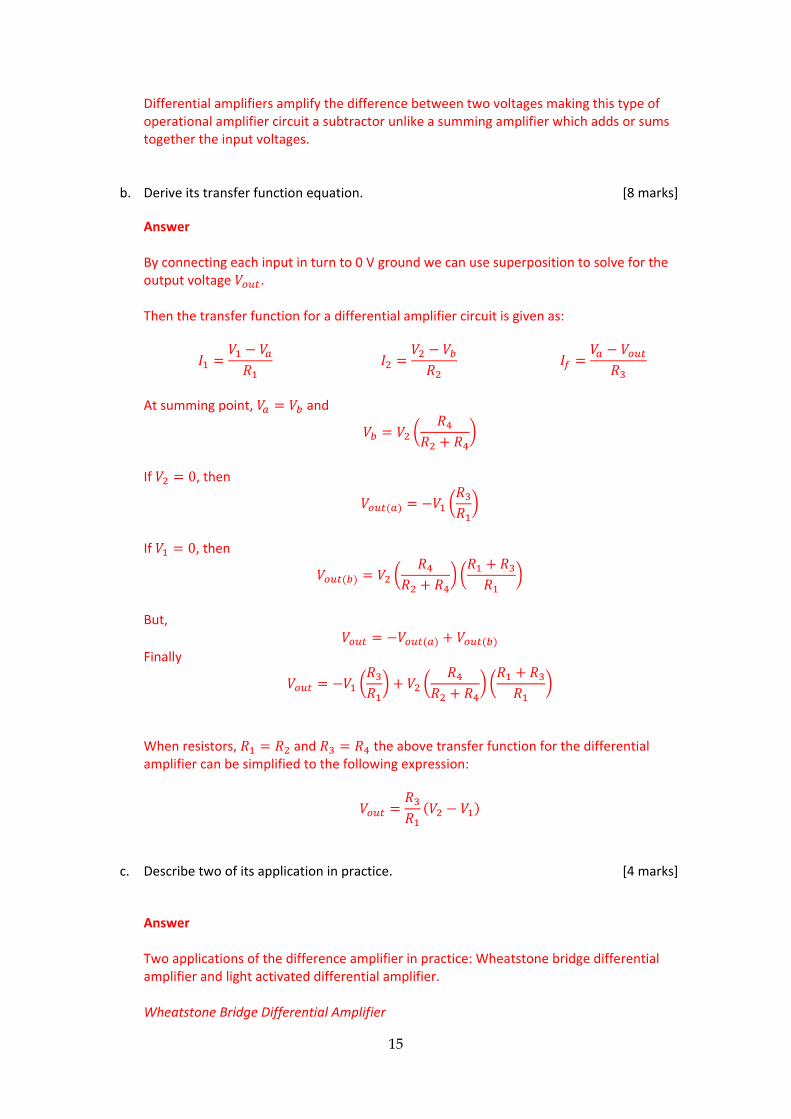
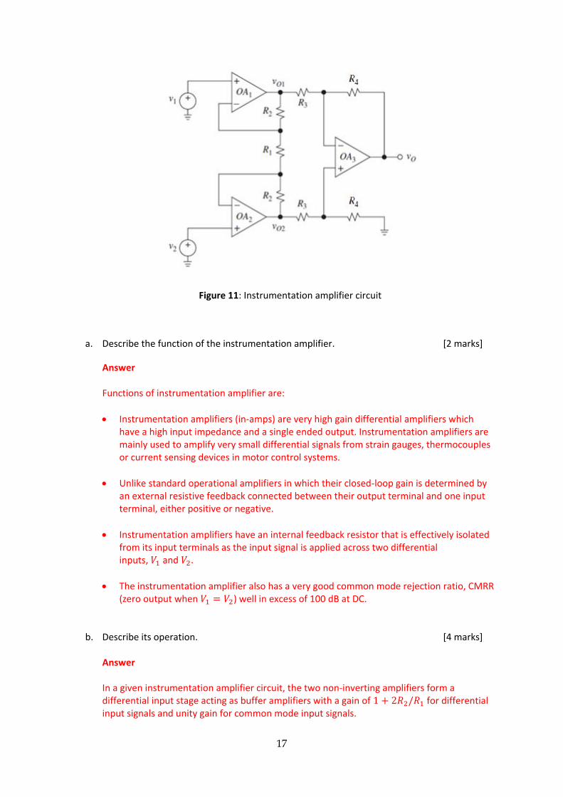
10. For a commonly found example of an instrumentation amplifier as shown in the figure below:
17
Figure 11: Instrumentation amplifier circuit
a. Describe the function of the instrumentation amplifier. [2 marks]
Answer Functions of instrumentation amplifier are:
Instrumentation amplifiers (in-amps) are very high gain differential amplifiers which have a high input impedance and a single ended output. Instrumentation amplifiers are mainly used to amplify very small differential signals from strain gauges, thermocouples or current sensing devices in motor control systems.
Unlike standard operational amplifiers in which their closed-loop gain is determined by an external resistive feedback connected between their output terminal and one input terminal, either positive or negative.
Instrumentation amplifiers have an internal feedback resistor that is effectively isolated from its input terminals as the input signal is applied across two differential inputs, 𝑉1 and 𝑉2.
The instrumentation amplifier also has a very good common mode rejection ratio, CMRR (zero output when 𝑉1 = 𝑉2) well in excess of 100 dB at DC.
b. Describe its operation. [4 marks]
Answer In a given instrumentation amplifier circuit, the two non-inverting amplifiers form a differential input stage acting as buffer amplifiers with a gain of 1 + 2𝑅2/𝑅1 for differential input signals and unity gain for common mode input signals.
18
Since amplifiers 𝑂𝐴1 and 𝑂𝐴2 are closed loop negative feedback amplifiers, we can expect the voltage at 𝑉𝑂1 to be equal to the input voltage 𝑉1. Likewise, the voltage at 𝑉𝑂2 to be equal to the value at 𝑉2. As the op-amps take no current at their input terminals (virtual earth), the same current must flow through the three resistors network of 𝑅2, 𝑅1 and 𝑅2 connected across the op-amp outputs. This means then that the voltage on the upper end of 𝑅1 will be equal to 𝑉1 and the voltage at the lower end of 𝑅1 to be equal to 𝑉2. This produces a voltage drop across resistor 𝑅1 which is equal to the voltage difference between inputs 𝑉1 and 𝑉2, the differential input voltage. Because the voltage at the summing junction of each amplifier, 𝑉𝑂1 and 𝑉𝑂2 is equal to the voltage applied to its positive inputs. However, if a common-mode voltage is applied to the amplifiers inputs, the voltages on each side of 𝑅1 will be equal, and no current will flow through this resistor. Since no current flows through 𝑅1 (nor, therefore, through both 𝑅2 resistors, amplifiers 𝐴1 and 𝐴2 will operate as unity-gain followers (buffers). Since the input voltage at the outputs of amplifiers 𝐴1 and 𝐴2 appears differentially across the three resistors network, the differential gain of the circuit can be varied by just changing the value of 𝑅1. The voltage output from the differential op-amp 𝐴3 acting as a subtractor, is simply the difference between its two inputs ( 𝑉2 − 𝑉1) and which is amplified by the gain of 𝐴3 which may be one, unity, (assuming that 𝑅3 = 𝑅4).
c. State its transfer function equation. [ 2 marks]
Answer Transfer function equation of the instrumentation amplifier is based on a general expression for overall voltage gain of the instrumentation amplifier circuit as:
𝑉𝑜𝑢𝑡 = (𝑉2 − 𝑉1) (1 +2𝑅2
𝑅1) (
𝑅4
𝑅3)
D. Op Amp based Circuits II
11. Consider the comparator circuit shown in the figure below, whose output saturates at ±13 V.
19
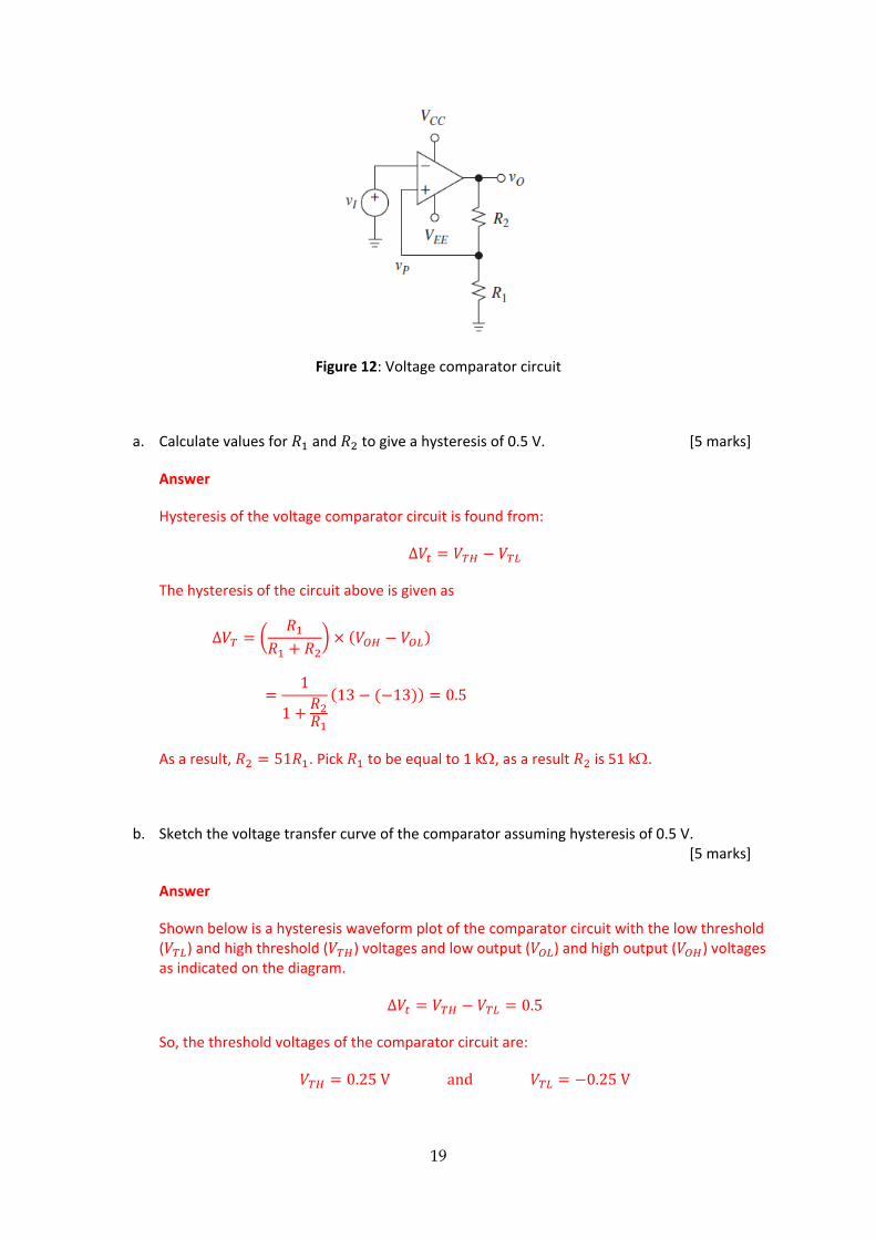
Figure 12: Voltage comparator circuit
a. Calculate values for 𝑅1 and 𝑅2 to give a hysteresis of 0.5 V. [5 marks]
Answer
Hysteresis of the voltage comparator circuit is found from:
∆𝑉𝑡 = 𝑉𝑇𝐻 − 𝑉𝑇𝐿
The hysteresis of the circuit above is given as
∆𝑉𝑇 = (𝑅1
𝑅1 + 𝑅2) × (𝑉𝑂𝐻 − 𝑉𝑂𝐿)
=1
1 +𝑅2𝑅1
(13 − (−13)) = 0.5
As a result, 𝑅2 = 51𝑅1. Pick 𝑅1 to be equal to 1 k, as a result 𝑅2 is 51 k.
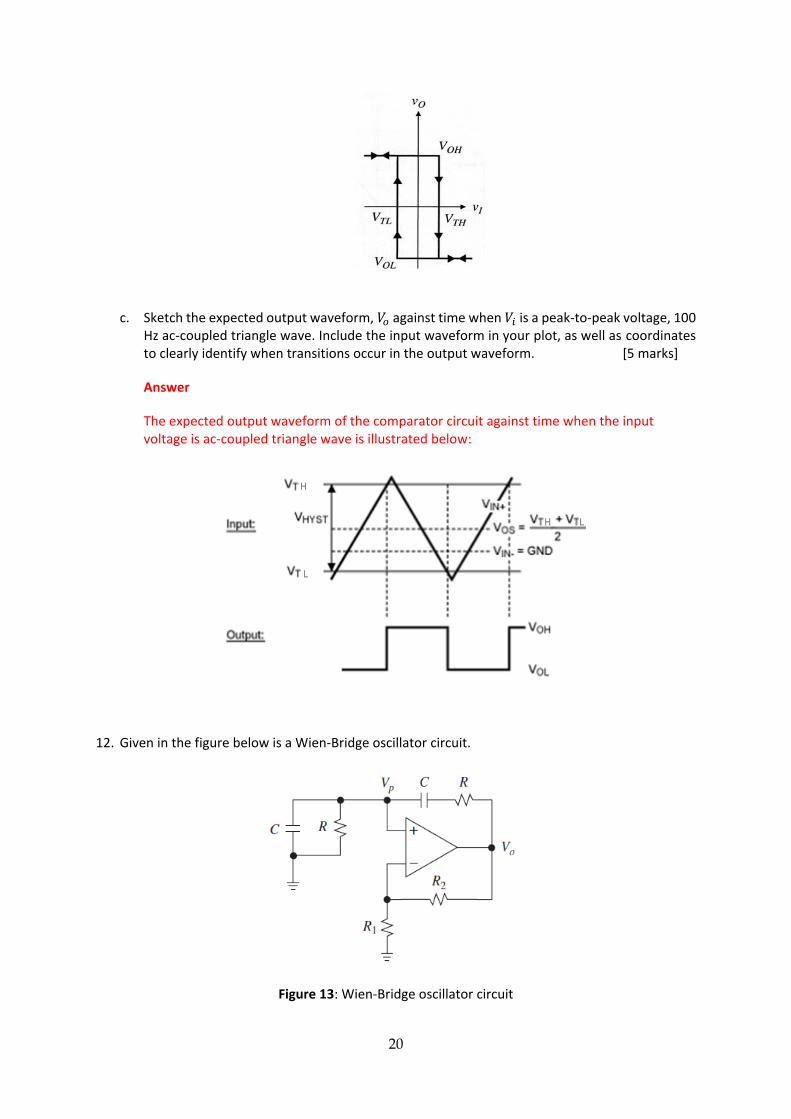
b. Sketch the voltage transfer curve of the comparator assuming hysteresis of 0.5 V. [5 marks]
Answer
Shown below is a hysteresis waveform plot of the comparator circuit with the low threshold (𝑉𝑇𝐿) and high threshold (𝑉𝑇𝐻) voltages and low output (𝑉𝑂𝐿) and high output (𝑉𝑂𝐻) voltages as indicated on the diagram.
∆𝑉𝑡 = 𝑉𝑇𝐻 − 𝑉𝑇𝐿 = 0.5
So, the threshold voltages of the comparator circuit are:
𝑉𝑇𝐻 = 0.25 V and 𝑉𝑇𝐿 = −0.25 V
20
c. Sketch the expected output waveform, 𝑉𝑜 against time when 𝑉𝑖 is a peak-to-peak voltage, 100 Hz ac-coupled triangle wave. Include the input waveform in your plot, as well as coordinates to clearly identify when transitions occur in the output waveform. [5 marks]
Answer
The expected output waveform of the comparator circuit against time when the input voltage is ac-coupled triangle wave is illustrated below:
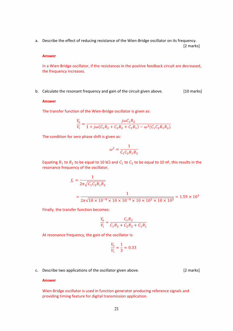
12. Given in the figure below is a Wien-Bridge oscillator circuit.
Figure 13: Wien-Bridge oscillator circuit
21
a. Describe the effect of reducing resistance of the Wien-Bridge oscillator on its frequency. [2 marks]
Answer
In a Wien-Bridge oscillator, if the resistances in the positive feedback circuit are decreased, the frequency increases.
b. Calculate the resonant frequency and gain of the circuit given above. [10 marks]
Answer
The transfer function of the Wien-Bridge oscillator is given as:
𝑉𝑜
𝑉𝑖=
𝑗𝜔𝐶1𝑅2
1 + 𝑗𝜔(𝐶1𝑅2 + 𝐶2𝑅2 + 𝐶1𝑅1) − 𝜔2(𝐶1𝐶2𝑅1𝑅2)
The condition for zero phase shift is given as:
𝜔2 =1
𝐶1𝐶2𝑅1𝑅2
Equating 𝑅1 to 𝑅2 to be equal to 10 k and 𝐶1 to 𝐶2 to be equal to 10 nF, this results in the resonance frequency of the oscillator,
𝑓𝑟 =1
2𝜋√𝐶1𝐶2𝑅1𝑅2
=1
2𝜋√10 × 10−9 × 10 × 10−9 × 10 × 103 × 10 × 103= 1.59 × 10³
Finally, the transfer function becomes:
𝑉𝑜
𝑉𝑖=
𝐶1𝑅2
𝐶1𝑅2 + 𝐶2𝑅2 + 𝐶1𝑅1
At resonance frequency, the gain of the oscillator is:
𝑉𝑜
𝑉𝑖=
1
3= 0.33
c. Describe two applications of the oscillator given above. [2 marks]
Answer Wien-Bridge oscillator is used in function generator producing reference signals and providing timing feature for digital transmission application.
22
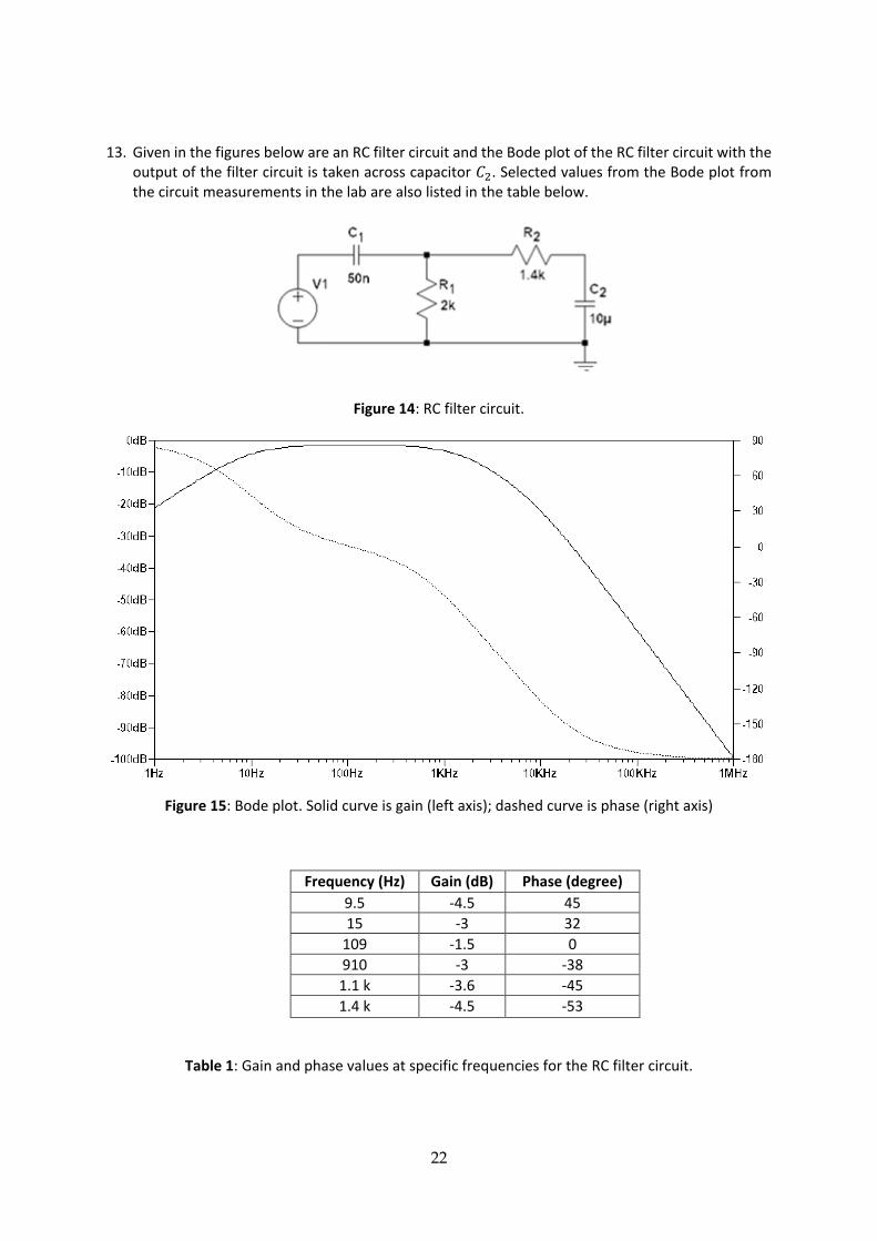
13. Given in the figures below are an RC filter circuit and the Bode plot of the RC filter circuit with the output of the filter circuit is taken across capacitor 𝐶2. Selected values from the Bode plot from the circuit measurements in the lab are also listed in the table below.
Figure 14: RC filter circuit.
Figure 15: Bode plot. Solid curve is gain (left axis); dashed curve is phase (right axis)
Frequency (Hz) Gain (dB) Phase (degree)
9.5 -4.5 45
15 -3 32
109 -1.5 0
910 -3 -38
1.1 k -3.6 -45
1.4 k -4.5 -53
Table 1: Gain and phase values at specific frequencies for the RC filter circuit.
23
a. Calculate the cut-off frequency of the filter circuit above. [10 marks]
Answer
The band-pass filter circuit as given above can be treated as two stages filter that consists of high-pass and low-pass filters.
Upper cut-off frequency of the filter stage:
𝑓𝐻 =1
2𝜋𝐶2𝑅2=
1
2𝜋 × 50 × 10−9 × 2 × 103= 1.592 × 10³ Hz
Lower cut-off frequency of the filter stage:
𝑓𝐿 =1
2𝜋𝐶1𝑅1=
1
2𝜋 × 10 × 10−6 × 1.4 × 103= 11.37 Hz
As a result, the upper and lower cut-off frequencies of the band-pass filter are 1.592 kHz and 11.37 Hz respectively.
b. From the table and graph, find the high-pass cut-off frequency for this filter is. [2 marks]
Answer
The cut-off frequency of the filter circuit is approximately 9.5 Hz from the table and graph.
c. Explain the difference between the calculated and the measured values. [2 marks]
Answer
The differences are due to tolerances of the components used in the filter circuit and also due to errors of testing instruments used in measuring the variables.
14. For a given low-pass Sallen-Key active filter shown in the figure below.
Figure 16: Sallen-Key based low-pass filter circuit
24
a. For an active filter used for attenuating signal application, which of the standardized filter design e.g. Butterworth, Bessel, and Chebyshev will be best to realize a stop band filter. Give a reason for your answer. [2 marks]
Answer
For a given active filter, the order for the best design of signal attenuation application is the Chebyshev Type II. The reason is Chebyshev response filter has the sharpest roll-off slope compared with other standard filters. The stop band response can be realized more precisely with this type of filter with narrower cut-off frequency of the filter. Furthermore, the ripples that exist in the stop band (e.g. due to type II Chebyshev response filter) could be useful for maximizing signal attenuation.
b. Compare passive and active filters. Give an advantage for each and state applications were each type of filter are particularly well suited. [5 marks]
Answer
Comparison between passive and active filters:
Advantage:
Passive filter: more precise design outcome and cost effective.
Active filter: design flexibilities and application beyond conventional usages.
Application:
Passive filter: application that requires more precise result
Active filter: application that requires advanced signal treatment e.g. amplification, conversion, rectification, etc.
c. Calculate the cut-off frequency and 𝑄-factor for the low-pass Sallen-Key filter shown in figure given above, where 𝑅1 = 1600 Ω, 𝑅2 = 400 Ω, 𝐶1 = 40 nF, and 𝐶2 = 10 nF. [10 marks]
Answer
Cut-off frequency of the low-pass Sallen-Key filter:
𝑓𝑐 =1
√𝑅1𝑅2𝐶1𝐶2
=1
√1600 × 400 × 40 × 10−9 × 10 × 10−9
= 62,500 rad/sec = 9,947Hz
25
𝑄-factor of the low-pass Sallen-Key filter:
𝑄 =1
𝑅1 + 𝑅2√𝑅1𝑅2
𝐶1
𝐶2
=1
1600 + 400√1600 × 400 ×
40 × 10−9
10 × 10−9
= 0.8
26
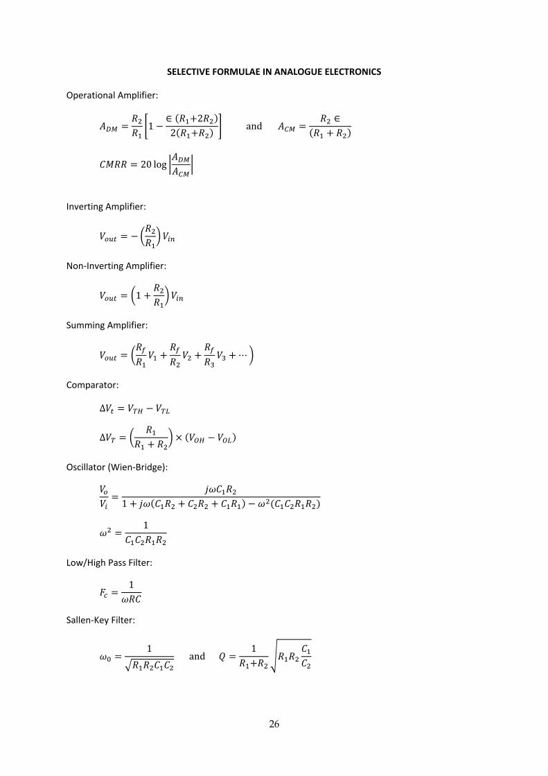
SELECTIVE FORMULAE IN ANALOGUE ELECTRONICS
Operational Amplifier:
𝐴𝐷𝑀 =𝑅2
𝑅1[1 −
∈ (𝑅1+2𝑅2)
2(𝑅1+𝑅2)] and 𝐴𝐶𝑀 =
𝑅2 ∈
(𝑅1 + 𝑅2)
𝐶𝑀𝑅𝑅 = 20 log |𝐴𝐷𝑀
𝐴𝐶𝑀|
Inverting Amplifier:
𝑉𝑜𝑢𝑡 = − (𝑅2
𝑅1) 𝑉𝑖𝑛
Non-Inverting Amplifier:
𝑉𝑜𝑢𝑡 = (1 +𝑅2
𝑅1) 𝑉𝑖𝑛
Summing Amplifier:
𝑉𝑜𝑢𝑡 = (𝑅𝑓
𝑅1𝑉1 +
𝑅𝑓
𝑅2𝑉2 +
𝑅𝑓
𝑅3𝑉3 + ⋯ )
Comparator:
∆𝑉𝑡 = 𝑉𝑇𝐻 − 𝑉𝑇𝐿
∆𝑉𝑇 = (𝑅1
𝑅1 + 𝑅2) × (𝑉𝑂𝐻 − 𝑉𝑂𝐿)
Oscillator (Wien-Bridge):
𝑉𝑜
𝑉𝑖=
𝑗𝜔𝐶1𝑅2
1 + 𝑗𝜔(𝐶1𝑅2 + 𝐶2𝑅2 + 𝐶1𝑅1) − 𝜔2(𝐶1𝐶2𝑅1𝑅2)
𝜔2 =1
𝐶1𝐶2𝑅1𝑅2
Low/High Pass Filter:
𝐹𝑐 =1
𝜔𝑅𝐶
Sallen-Key Filter:
𝜔0 =1
√𝑅1𝑅2𝐶1𝐶2
and 𝑄 =1
𝑅1+𝑅2√𝑅1𝑅2
𝐶1
𝐶2