Embed Size (px)
DESCRIPTION
75 GHz 80 mW InP DHBT Power Amplifier. Y. Wei, M. Urteaga, Z. Griffith, D. Scott, S. Xie, V. Paidi, N. Parthasarathy, M. Rodwell. Department of Electrical and Computer Engineering, University of California, Santa Barbara. - PowerPoint PPT Presentation
Citation preview
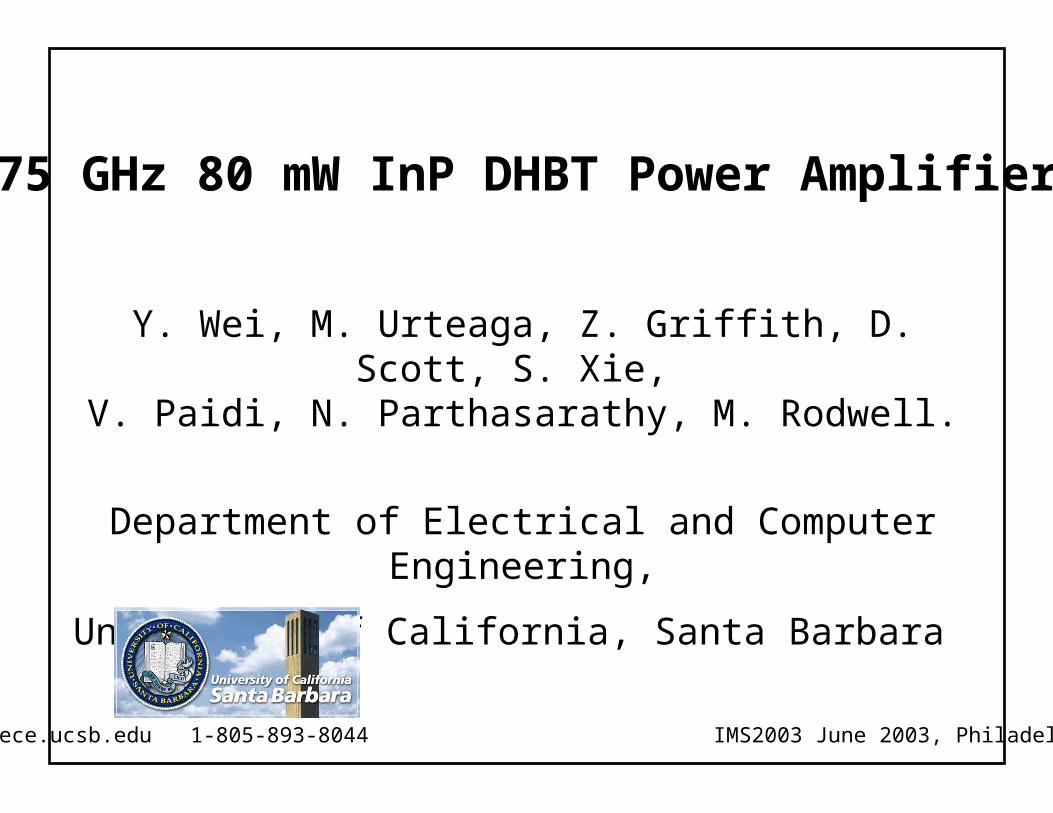
Y. Wei, M. Urteaga, Z. Griffith, D. Scott, S. Xie, V. Paidi, N. Parthasarathy, M. Rodwell.
Department of Electrical and Computer Engineering,
University of California, Santa Barbara
[email protected] 1-805-893-8044 IMS2003 June 2003, Philadelphia, PA
75 GHz 80 mW InP DHBT Power Amplifier
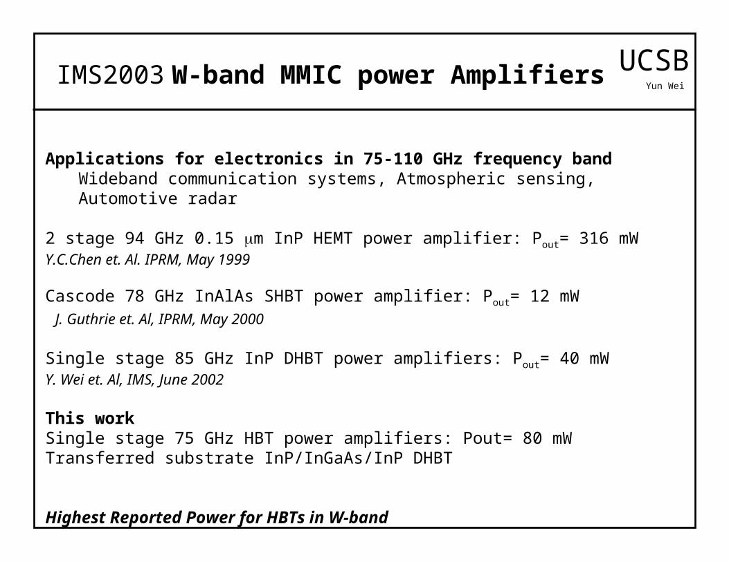
W-band MMIC power AmplifiersIMS2003
Applications for electronics in 75-110 GHz frequency bandWideband communication systems, Atmospheric sensing, Automotive radar
2 stage 94 GHz 0.15 m InP HEMT power amplifier: Pout= 316 mW Y.C.Chen et. Al. IPRM, May 1999
Cascode 78 GHz InAlAs SHBT power amplifier: Pout= 12 mW J. Guthrie et. Al, IPRM, May 2000 Single stage 85 GHz InP DHBT power amplifiers: Pout= 40 mW Y. Wei et. Al, IMS, June 2002
This workSingle stage 75 GHz HBT power amplifiers: Pout= 80 mWTransferred substrate InP/InGaAs/InP DHBT
Highest Reported Power for HBTs in W-band
UCSBYun Wei
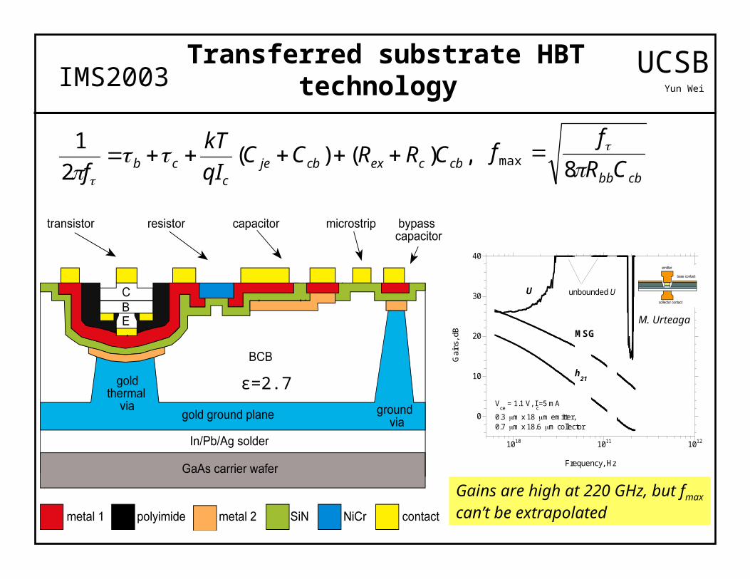
Transferred substrate HBT technologyIMS2003
ε=2.7
UCSBYun Wei
Gains are high at 220 GHz, but fmax can’t be extrapolated
0
10
20
30
40
1010 1011 1012
Gai
ns, d
BFrequency, Hz
U
h21
MSG
unbounded U
Vce
= 1.1 V, Ic=5 mA
0.3 m x 18 m emitter,0.7 m x 18.6 m collector
M. Urteaga
,)()(2
1cbcexcbje
ccb CRRCC
qI
kT
f
cbbbCR
ff
8max
-30
-20
-10
0
10
20
140 150 160 170 180 190 200 210 220
S21S11S22
dB
frequency (GHz)
0
10
20
30
40
1 10 100 1000
Gai
ns (
dB)
Frequency (GHz)
U
h21 462
395
343
139
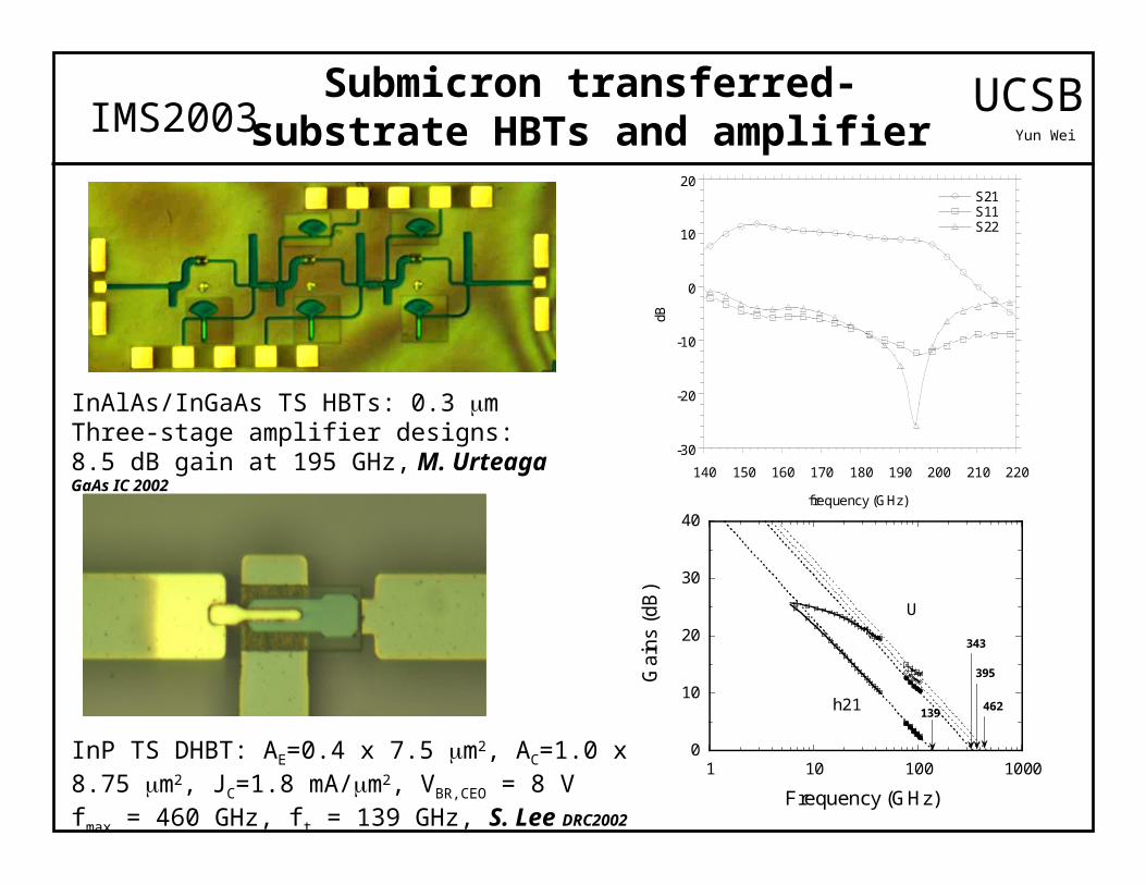
InP TS DHBT: AE=0.4 x 7.5 m2, AC=1.0 x 8.75 m2, JC=1.8 mA/m2, VBR,CEO = 8 V fmax = 460 GHz, ft = 139 GHz, S. Lee DRC2002
InAlAs/InGaAs TS HBTs: 0.3 m Three-stage amplifier designs: 8.5 dB gain at 195 GHz, M. Urteaga GaAs IC 2002
Submicron transferred-substrate HBTs and amplifier IMS2003 UCSB
Yun Wei
-5
0
5
10
15
20
0
2
4
6
8
10
-15 -10 -5 0 5 10 15
Po
ut,
dB
m GT , d
B
Pin, dBm
GT Pout
IMS2003 UCSBYun Wei
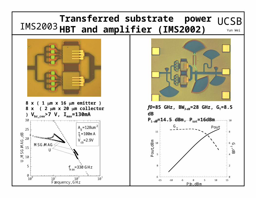
8 x ( 1 m x 16 m emitter )8 x ( 2 m x 20 m collector ) Vbr_ceo>7 V, Imax=130mA
f0=85 GHz, BW3-dB=28 GHz, GT=8.5 dBP1-dB=14.5 dBm, Psat=16dBm
Transferred substrate power HBT and amplifier (IMS2002)
Q1 Q2 Q3 Q4
C
E
I0-i I0+i I0-iI0+i
Rex
Q1 Q2 Q3 Q4
C
E
Rdist I0 Rdist I0 Rdist I0 Rdist I0
Rex
common mode
f1 f2 f3 f4
I0
I0
0
differential mode
current hogging
Ic
collector
emitterbase
sub-collector
current
temperature
f1f2f3f4
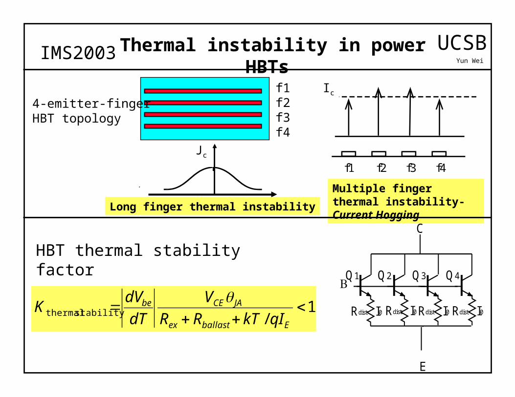
4-emitter-finger HBT topology
Jc
Multiple finger thermal instability- Current HoggingLong finger thermal instability
1/stability thermal
Eballastex
JACEbe
qIkTRR
V
dT
dVK
Thermal instability in power HBTsIMS2003 UCSBYun Wei
HBT thermal stability factor
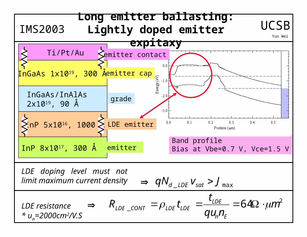
Band profileBias at Vbe=0.7 V, Vce=1.5 V
Long emitter ballasting: Lightly doped emitter expitaxy
* un=2000cm2/V.S
max_ JvqN satLDEd LDE doping level must not limit maximum current density
2_ 64 m
nqu
ttR
En
LDELDELDECONTLDE LDE resistance
emitter capInGaAs 1x10¹⁹, 300 Å
InGaAs/InAlAs 2x10¹⁹, 90 Å
InP 5x10¹⁶, 1000 Å
InP 8x10¹⁷, 300 Å
grade
LDE emitter
emitter
emitter contactTi/Pt/Au
IMS2003 UCSBYun Wei
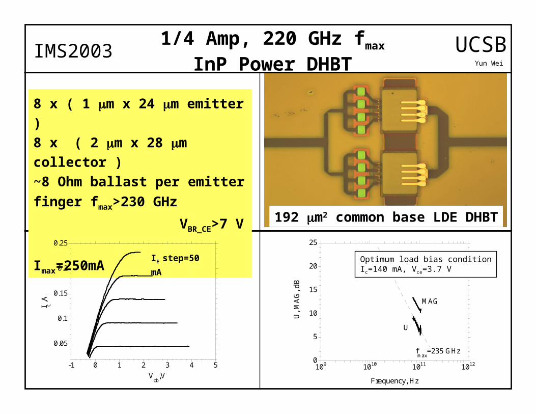
1/4 Amp, 220 GHz fmax InP Power DHBT
UCSBYun Wei
192 m2 common base LDE DHBT
8 x ( 1 m x 24 m emitter )
8 x ( 2 m x 28 m collector )
~8 Ohm ballast per emitter finger
fmax>230 GHz
VBR_CE>7 V
Imax=250mA
0.05
0.1
0.15
0.2
0.25
-1 0 1 2 3 4 5
I C,A
Vcb
,V
0
5
10
15
20
25
109 1010 1011 1012
U, M
AG
, dB
Frequency, Hz
U
MAG
fmax
=235 GHz
Optimum load bias conditionIc=140 mA, Vce=3.7 V
IMS2003
IE step=50 mA
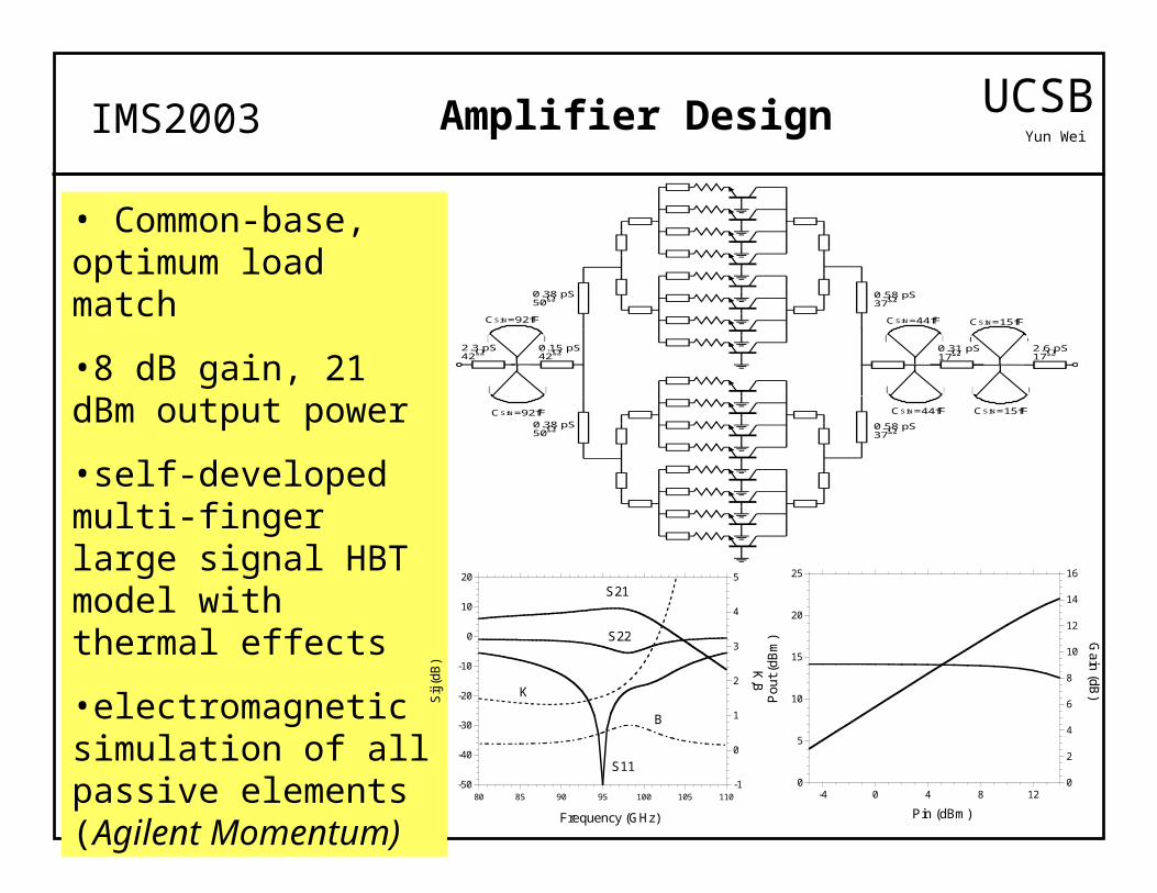
• Common-base, optimum load match
•8 dB gain, 21 dBm output power
•self-developed multi-finger large signal HBT model with thermal effects
•electromagnetic simulation of all passive elements (Agilent Momentum)
Amplifier DesignIMS2003
2.6 pS17
0.31 pS17
0.15 pS42
2.3 pS42
0.38 pS50
0.38 pS50 0.58 pS
37
0.58 pS37
CSiN=92fF
CSiN=92fF
CSiN=44fF
CSiN=44fF
CSiN=15fF
CSiN=15fF
-50
-40
-30
-20
-10
0
10
20
-1
0
1
2
3
4
5
80 85 90 95 100 105 110
Sij
(dB
) K,B
Frequency (GHz)
S21
S22
S11
B
K
0
5
10
15
20
25
0
2
4
6
8
10
12
14
16
-4 0 4 8 12
Po
ut (
dBm
) Gain
(dB)
Pin (dBm)
UCSBYun Wei
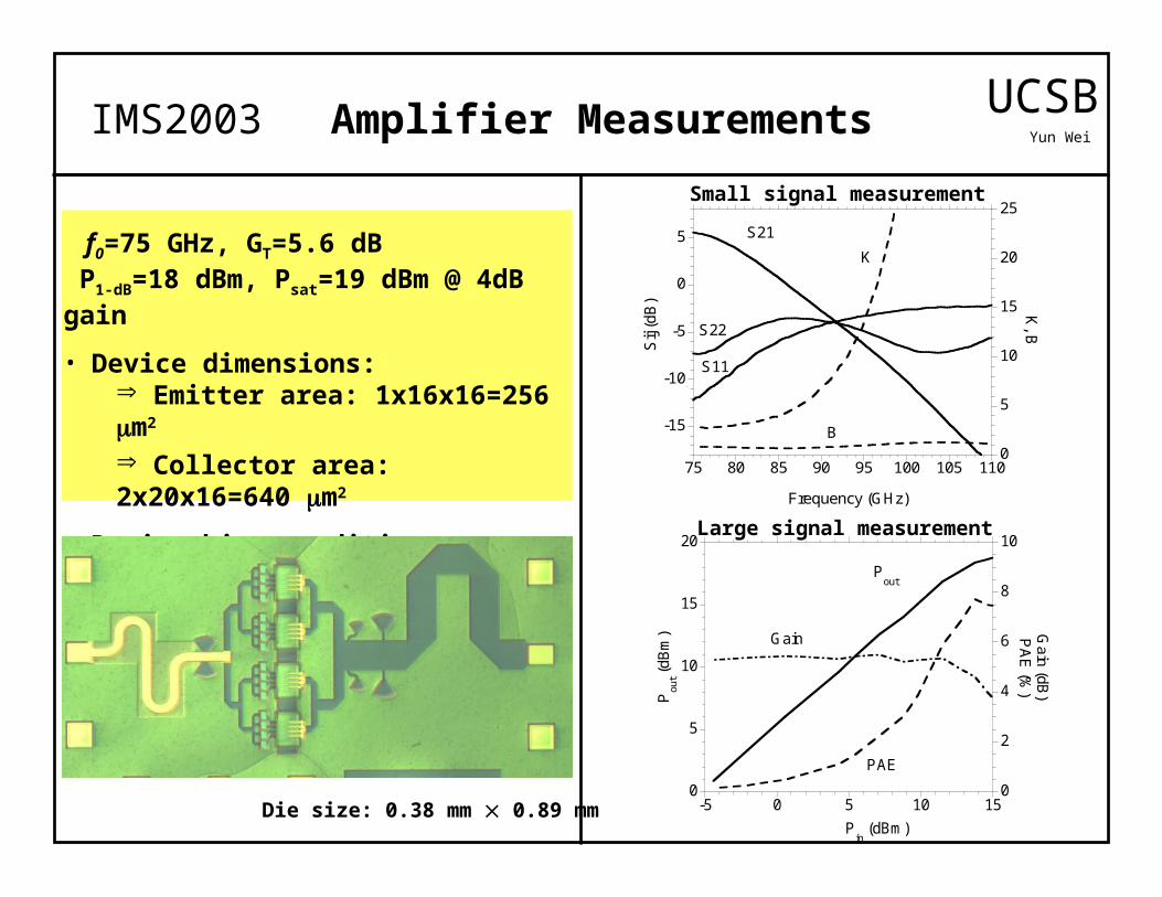
Amplifier Measurements
f0=75 GHz, GT=5.6 dB P1-dB=18 dBm, Psat=19 dBm @ 4dB gain
• Device dimensions: Emitter area: 1x16x16=256 m2
Collector area: 2x20x16=640 m2
• Device bias conditions: Ic=130 mA, Vce=4.5 V
Small signal measurement
Large signal measurement
IMS2003
Die size: 0.38 mm 0.89 mm
-15
-10
-5
0
5
0
5
10
15
20
25
75 80 85 90 95 100 105 110
Frequency (GHz)
K, B
Sij
(dB
)
S21
S22
S11
B
K
0
5
10
15
20
0
2
4
6
8
10
-5 0 5 10 15
Pou
t (dB
m) G
ain (dB)
PA
E (%
)
Pin (dBm)
Gain
PAE
Pout
UCSBYun Wei
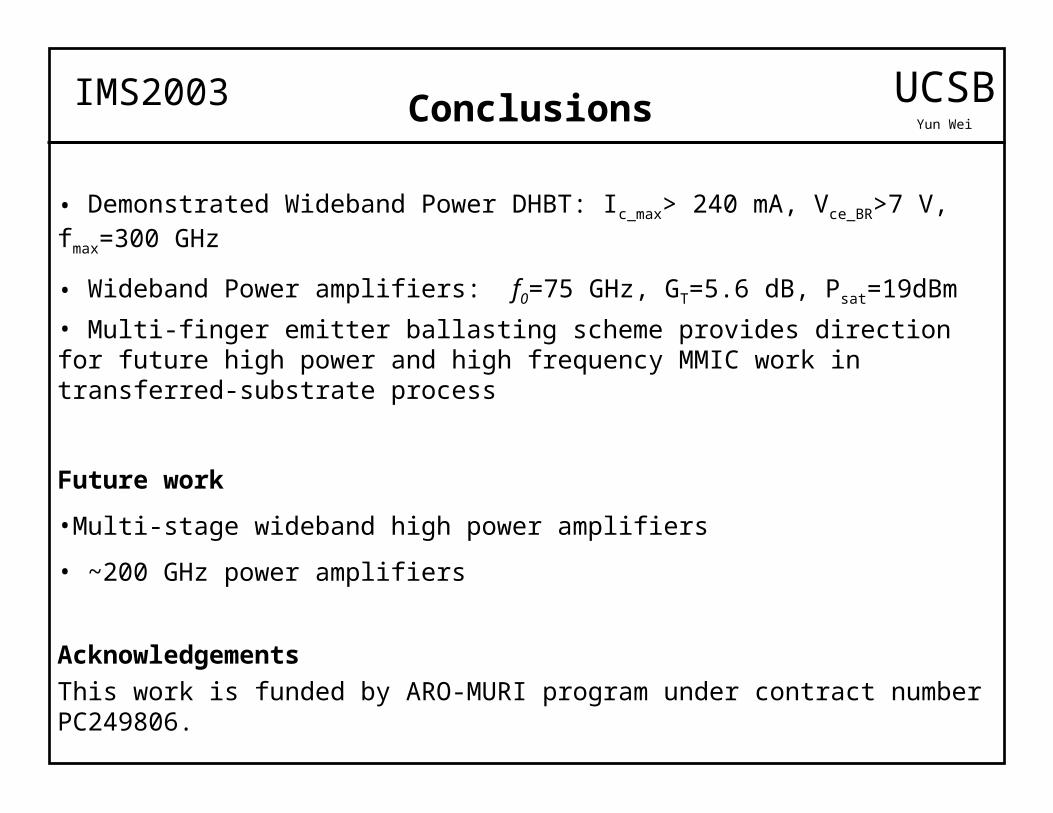
Conclusions
• Demonstrated Wideband Power DHBT: Ic_max> 240 mA, Vce_BR>7 V, fmax=300 GHz
• Wideband Power amplifiers: f0=75 GHz, GT=5.6 dB, Psat=19dBm
• Multi-finger emitter ballasting scheme provides direction for future high power and high frequency MMIC work in transferred-substrate process
Future work
•Multi-stage wideband high power amplifiers
• ~200 GHz power amplifiers
Acknowledgements
This work is funded by ARO-MURI program under contract number PC249806.
UCSBYun Wei
IMS2003