Embed Size (px)
Citation preview
Z. Feng MTU EE4800 CMOS Digital IC Design & Z. Feng MTU EE4800 CMOS Digital IC Design & AnalysisAnalysis
13.13.11
EE4800 CMOS Digital IC Design & Analysis
Lecture 13 Packaging, Power and Clock Distributions
Zhuo Feng
Z. Feng MTU EE4800 CMOS Digital IC Design & Z. Feng MTU EE4800 CMOS Digital IC Design & AnalysisAnalysis
13.13.22
Outline■Packaging■Power Distribution■Clock Distribution
Z. Feng MTU EE4800 CMOS Digital IC Design & Z. Feng MTU EE4800 CMOS Digital IC Design & AnalysisAnalysis
13.13.33
Packages■Package functions
►Electrical connection of signals and power from chip to board
►Little delay or distortion►Mechanical connection of chip to board►Removes heat produced on chip►Protects chip from mechanical damage►Compatible with thermal expansion► Inexpensive to manufacture and test
Z. Feng MTU EE4800 CMOS Digital IC Design & Z. Feng MTU EE4800 CMOS Digital IC Design & AnalysisAnalysis
13.13.44
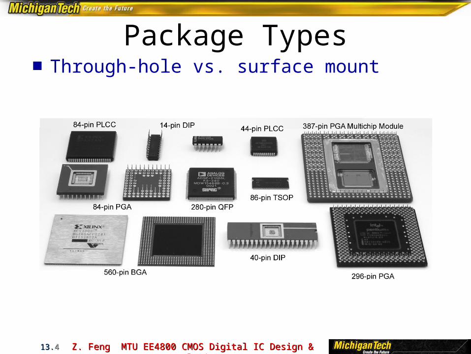
Package Types■Through-hole vs. surface mount
Z. Feng MTU EE4800 CMOS Digital IC Design & Z. Feng MTU EE4800 CMOS Digital IC Design & AnalysisAnalysis
13.13.55
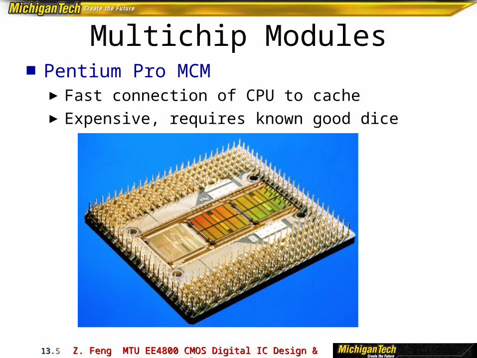
Multichip Modules■Pentium Pro MCM
►Fast connection of CPU to cache►Expensive, requires known good dice
Z. Feng MTU EE4800 CMOS Digital IC Design & Z. Feng MTU EE4800 CMOS Digital IC Design & AnalysisAnalysis
13.13.66
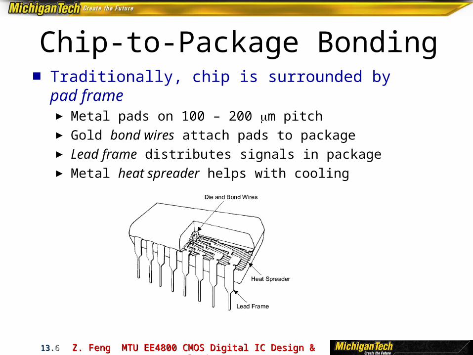
Chip-to-Package Bonding■ Traditionally, chip is surrounded by pad frame
► Metal pads on 100 – 200 m pitch► Gold bond wires attach pads to package► Lead frame distributes signals in package► Metal heat spreader helps with cooling
Z. Feng MTU EE4800 CMOS Digital IC Design & Z. Feng MTU EE4800 CMOS Digital IC Design & AnalysisAnalysis
13.13.77
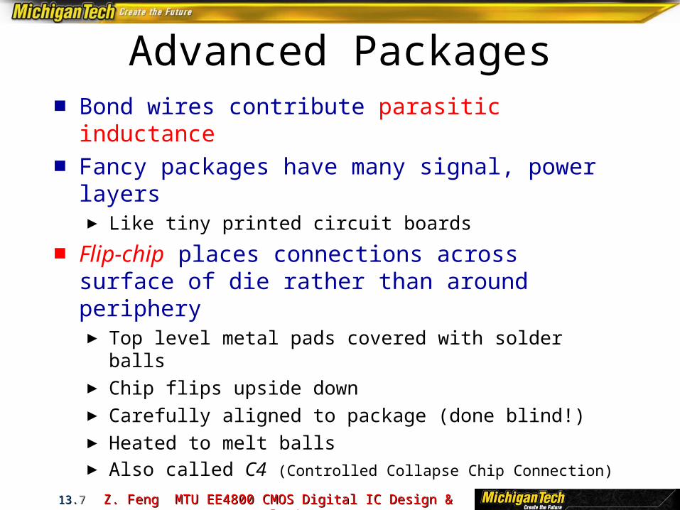
Advanced Packages■ Bond wires contribute parasitic inductance■ Fancy packages have many signal, power
layers► Like tiny printed circuit boards
■ Flip-chip places connections across surface of die rather than around periphery
► Top level metal pads covered with solder balls► Chip flips upside down► Carefully aligned to package (done blind!)► Heated to melt balls► Also called C4 (Controlled Collapse Chip Connection)
Z. Feng MTU EE4800 CMOS Digital IC Design & Z. Feng MTU EE4800 CMOS Digital IC Design & AnalysisAnalysis
13.13.88
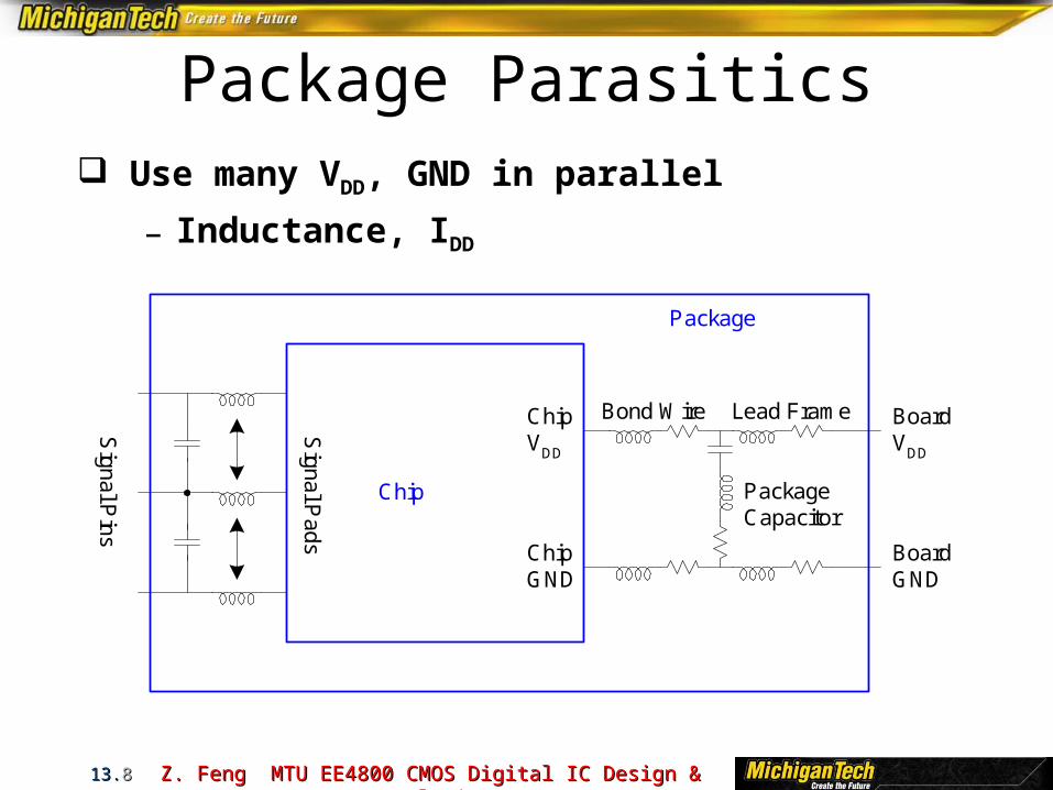
Package Parasitics
Chip
Signal P
ins
PackageCapacitor
Signal P
ads
ChipVDD
ChipGND
BoardVDD
BoardGND
Bond Wire Lead Frame
Package
Use many VDD, GND in parallel
– Inductance, IDD
Z. Feng MTU EE4800 CMOS Digital IC Design & Z. Feng MTU EE4800 CMOS Digital IC Design & AnalysisAnalysis
13.13.99
Heat Dissipation■ 60 W light bulb has surface area of 120 cm2
■ Itanium 2 die dissipates 130 W over 4 cm2
► Chips have enormous power densities► Cooling is a serious challenge
■ Package spreads heat to larger surface area► Heat sinks may increase surface area further► Fans increase airflow rate over surface area► Liquid cooling used in extreme cases ($$$)
Z. Feng MTU EE4800 CMOS Digital IC Design & Z. Feng MTU EE4800 CMOS Digital IC Design & AnalysisAnalysis
13.13.1010
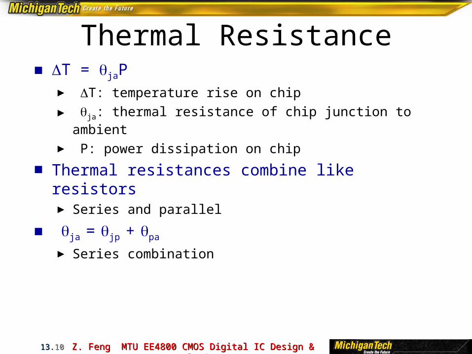
Thermal Resistance■ T = jaP
► T: temperature rise on chip
► ja: thermal resistance of chip junction to ambient
► P: power dissipation on chip
■ Thermal resistances combine like resistors► Series and parallel
■ ja = jp + pa
► Series combination
Z. Feng MTU EE4800 CMOS Digital IC Design & Z. Feng MTU EE4800 CMOS Digital IC Design & AnalysisAnalysis
13.13.1111
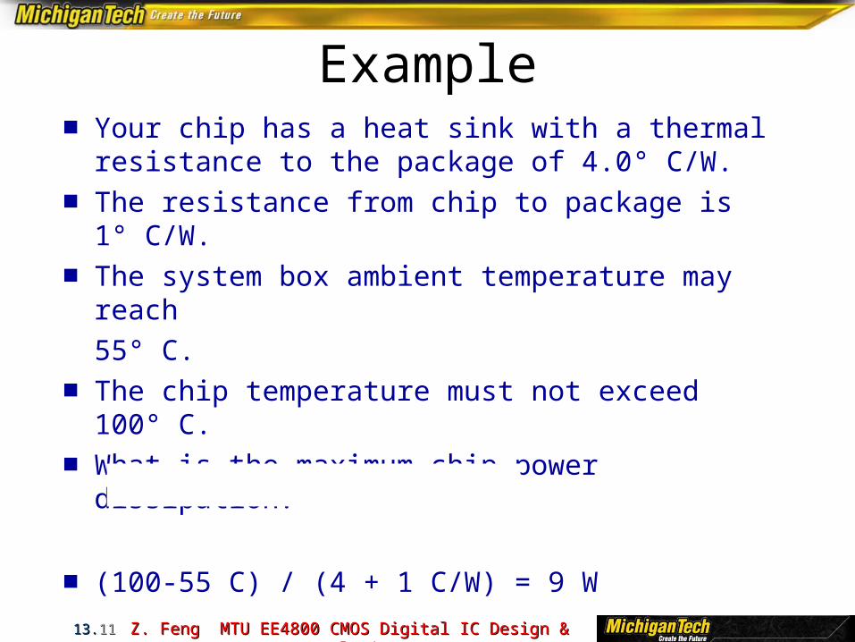
Example■ Your chip has a heat sink with a thermal
resistance to the package of 4.0° C/W. ■ The resistance from chip to package is 1° C/W.■ The system box ambient temperature may
reach 55° C.
■ The chip temperature must not exceed 100° C.■ What is the maximum chip power dissipation?
■ (100-55 C) / (4 + 1 C/W) = 9 W
Z. Feng MTU EE4800 CMOS Digital IC Design & Z. Feng MTU EE4800 CMOS Digital IC Design & AnalysisAnalysis
13.13.1212
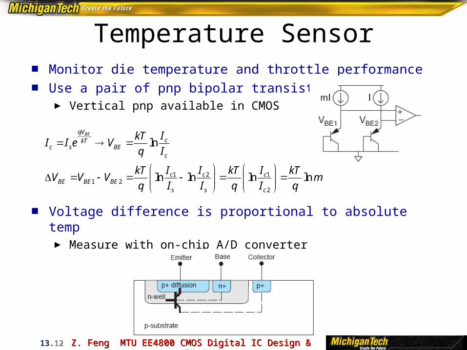
Temperature Sensor■ Monitor die temperature and throttle performance■ Use a pair of pnp bipolar transistors
► Vertical pnp available in CMOS
■ Voltage difference is proportional to absolute temp► Measure with on-chip A/D converter
1 2 11 2
2
ln
ln ln ln ln
BEqVckT
c s BEc
c c cBE BE BE
s s c
IkTI I e V
q I
I I IkT kT kTV V V m
q I I q I q
Z. Feng MTU EE4800 CMOS Digital IC Design & Z. Feng MTU EE4800 CMOS Digital IC Design & AnalysisAnalysis
13.13.1313
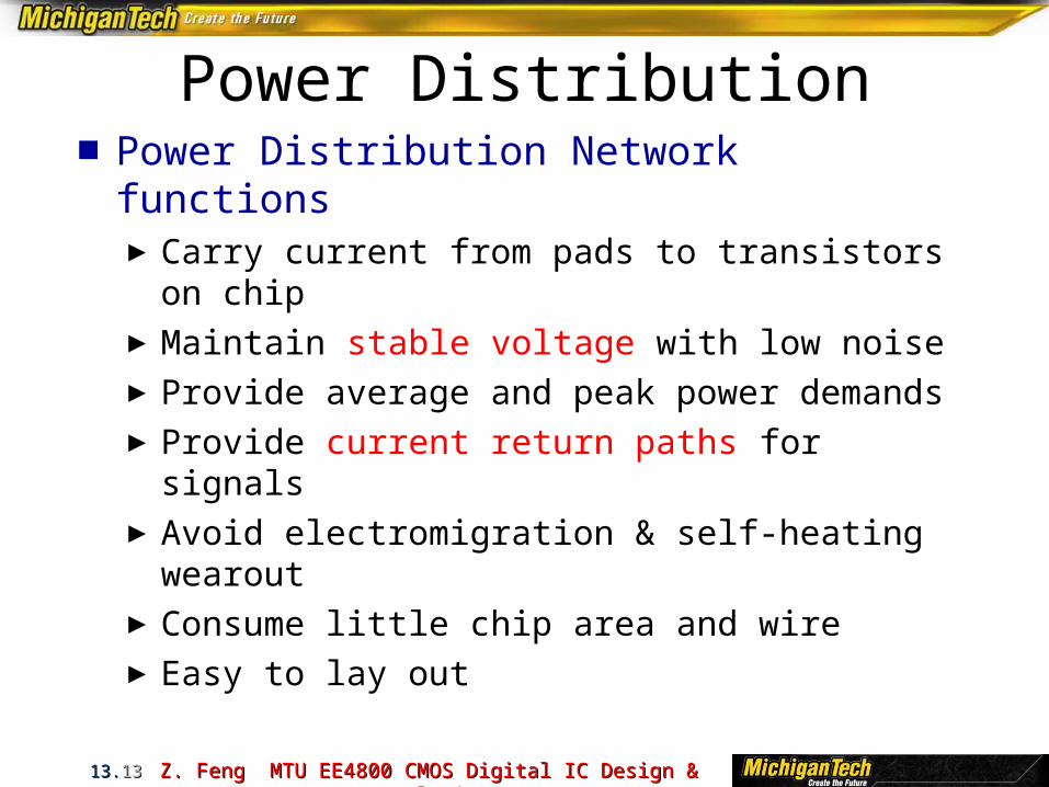
Power Distribution■Power Distribution Network functions
►Carry current from pads to transistors on chip►Maintain stable voltage with low noise►Provide average and peak power demands►Provide current return paths for signals►Avoid electromigration & self-heating wearout►Consume little chip area and wire►Easy to lay out
Z. Feng MTU EE4800 CMOS Digital IC Design & Z. Feng MTU EE4800 CMOS Digital IC Design & AnalysisAnalysis
13.13.1414
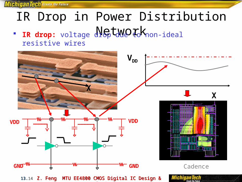
IR Drop in Power Distribution Network
VDD VDD
GNDGND
VDD
X
IR drop: voltage drop due to non-ideal resistive wires
X
Cadence
Z. Feng MTU EE4800 CMOS Digital IC Design & Z. Feng MTU EE4800 CMOS Digital IC Design & AnalysisAnalysis
13.13.1515
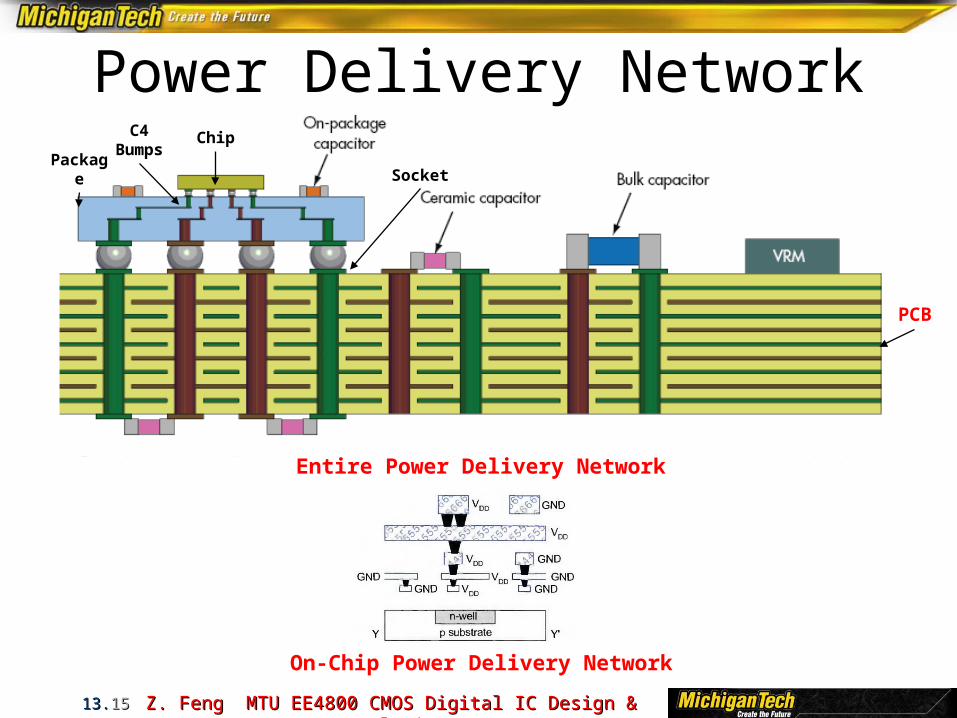
Power Delivery Network
Entire Power Delivery Network
On-Chip Power Delivery Network
PCB
Socket
ChipPackage
C4 Bumps
Z. Feng MTU EE4800 CMOS Digital IC Design & Z. Feng MTU EE4800 CMOS Digital IC Design & AnalysisAnalysis
13.13.1616
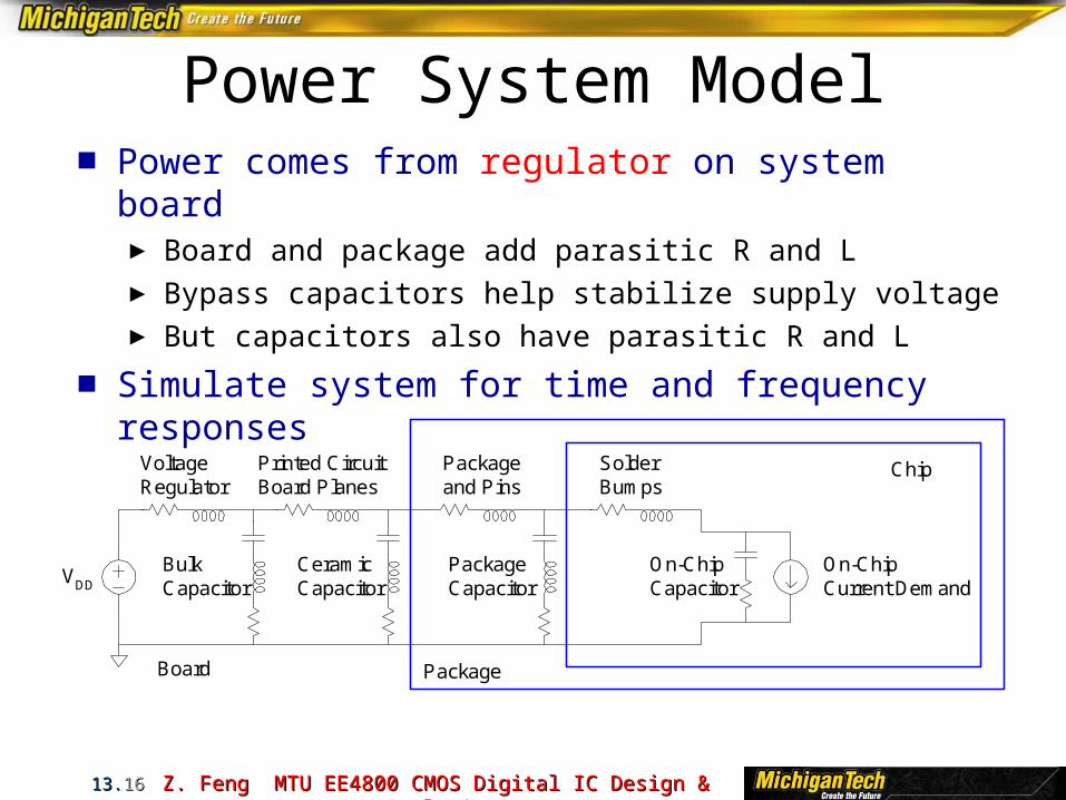
Power System Model■ Power comes from regulator on system board
► Board and package add parasitic R and L► Bypass capacitors help stabilize supply voltage► But capacitors also have parasitic R and L
■ Simulate system for time and frequency responses
VoltageRegulator
Printed CircuitBoard Planes
Packageand Pins
SolderBumps
BulkCapacitor
CeramicCapacitor
PackageCapacitor
On-ChipCapacitor
On-ChipCurrent Demand
VDD
Chip
PackageBoard
Z. Feng MTU EE4800 CMOS Digital IC Design & Z. Feng MTU EE4800 CMOS Digital IC Design & AnalysisAnalysis
13.13.1717
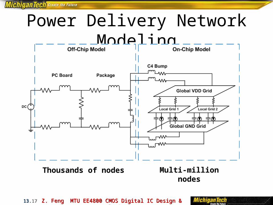
Power Delivery Network Modeling
Multi-million nodesThousands of nodes
Z. Feng MTU EE4800 CMOS Digital IC Design & Z. Feng MTU EE4800 CMOS Digital IC Design & AnalysisAnalysis
13.13.1818
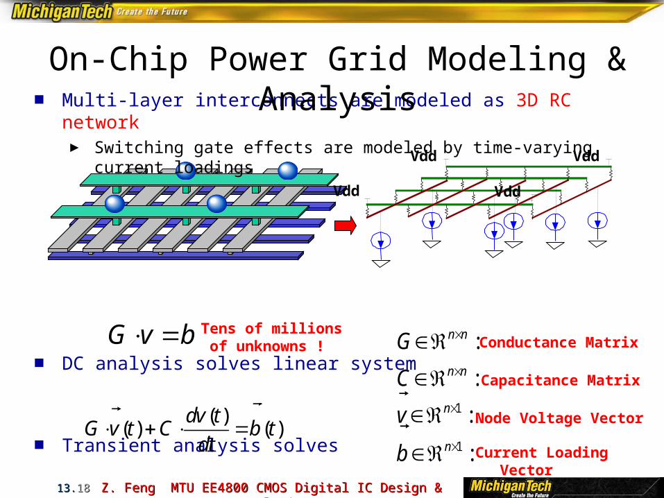
Vdd Vdd
Vdd Vdd
■ Multi-layer interconnects are modeled as 3D RC network► Switching gate effects are modeled by time-varying current loadings
■ DC analysis solves linear system
■ Transient analysis solves
On-Chip Power Grid Modeling & Analysis
Tens of millions of unknowns !
( )( ) ( )
dv tG v t C b t
dt
G v b
1
1
:
:
:
:
n n
n n
n
n
G
C
v
b
Conductance Matrix
Capacitance Matrix
Node Voltage Vector
Current Loading Vector
Z. Feng MTU EE4800 CMOS Digital IC Design & Z. Feng MTU EE4800 CMOS Digital IC Design & AnalysisAnalysis
13.13.1919
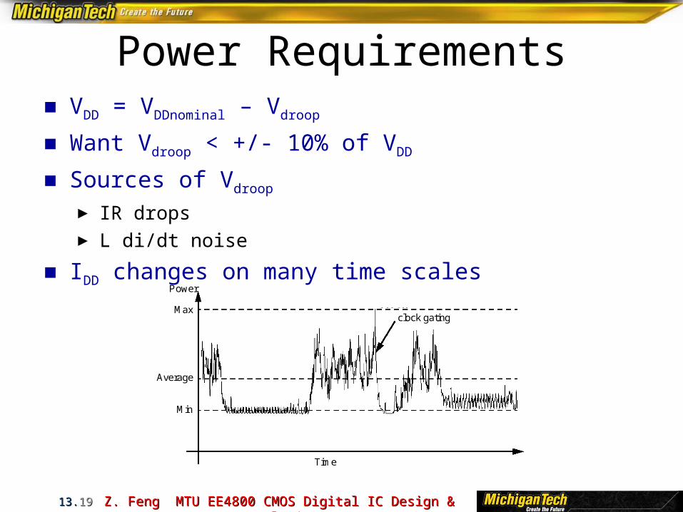
Power Requirements■ VDD = VDDnominal – Vdroop
■ Want Vdroop < +/- 10% of VDD
■ Sources of Vdroop
► IR drops► L di/dt noise
■ IDD changes on many time scales
clock gating
Time
Average
Max
Min
Power
Z. Feng MTU EE4800 CMOS Digital IC Design & Z. Feng MTU EE4800 CMOS Digital IC Design & AnalysisAnalysis
13.13.2020
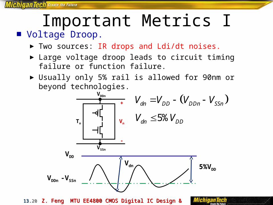
■ Voltage Droop.► Two sources: IR drops and Ldi/dt noises.► Large voltage droop leads to circuit timing failure or function
failure.► Usually only 5% rail is allowed for 90nm or beyond
technologies.
Important Metrics I
VDDn
VSSn
Tn
+
-
Vn
dn DD DDn SSnV V V V
5%dn DDV V
VDD
VDDn -VSSn
5%VD
D
Vdn
Z. Feng MTU EE4800 CMOS Digital IC Design & Z. Feng MTU EE4800 CMOS Digital IC Design & AnalysisAnalysis
13.13.2121
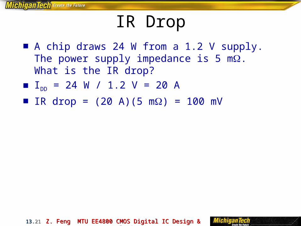
IR Drop■ A chip draws 24 W from a 1.2 V supply. The
power supply impedance is 5 m. What is the IR drop?
■ IDD = 24 W / 1.2 V = 20 A
■ IR drop = (20 A)(5 m) = 100 mV
Z. Feng MTU EE4800 CMOS Digital IC Design & Z. Feng MTU EE4800 CMOS Digital IC Design & AnalysisAnalysis
13.13.2222
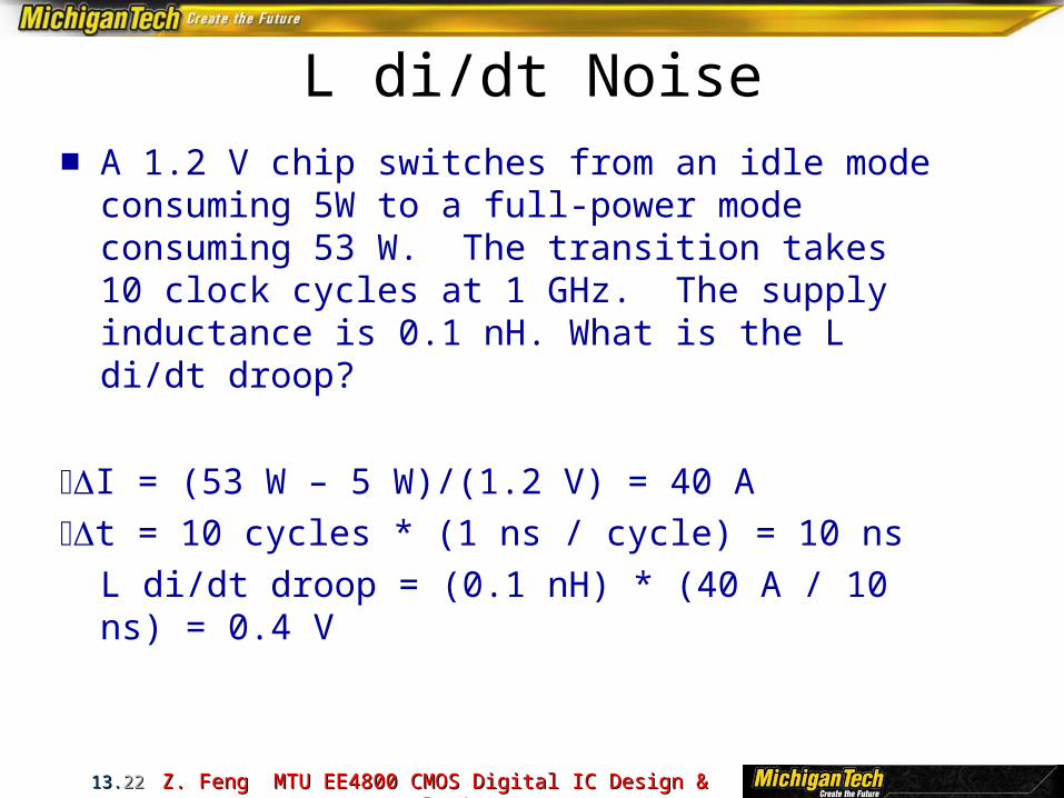
L di/dt Noise■ A 1.2 V chip switches from an idle mode
consuming 5W to a full-power mode consuming 53 W. The transition takes 10 clock cycles at 1 GHz. The supply inductance is 0.1 nH. What is the L di/dt droop?
I = (53 W – 5 W)/(1.2 V) = 40 At = 10 cycles * (1 ns / cycle) = 10 ns
L di/dt droop = (0.1 nH) * (40 A / 10 ns) = 0.4 V
Z. Feng MTU EE4800 CMOS Digital IC Design & Z. Feng MTU EE4800 CMOS Digital IC Design & AnalysisAnalysis
13.13.2323
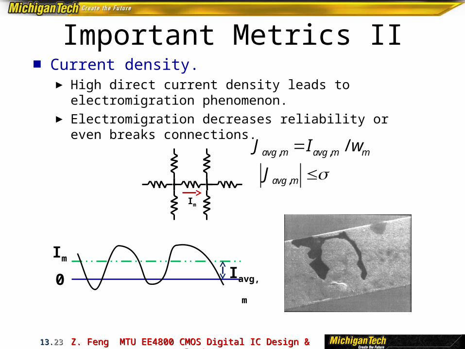
■ Current density.► High direct current density leads to electromigration
phenomenon.► Electromigration decreases reliability or even breaks
connections.
Important Metrics II
Im
, , /avg m avg m mJ I w
,avg mJ
0
Im
Iavg,
m
Z. Feng MTU EE4800 CMOS Digital IC Design & Z. Feng MTU EE4800 CMOS Digital IC Design & AnalysisAnalysis
13.13.2424
■ Scaled down supply voltage vs. increased operating frequency and power densities.
► Higher percentage of voltage droops.► Lower voltage droop tolerance.
■ Shrunk chip area vs. increased gated density.► Less wiring resources.► Larger power delivery network dimensions.
■ Fine-grained power management.► Power gating.► Multiple power domains.
Technology Scaling: Challenges
Z. Feng MTU EE4800 CMOS Digital IC Design & Z. Feng MTU EE4800 CMOS Digital IC Design & AnalysisAnalysis
13.13.2525
■ Simulation:► Stricter accuracy requirement.► More efficient in terms of runtime and memory.► Full chip simulation with package and integrated
components.
■ Verification:► Power-gated power delivery network with multiple power
gating configurations.
■ Design:► Optimization for wire sizing.► Detailed tradeoff analysis for on-chip voltage regulation.► Optimization for on-chip voltage regulation.
Technology Scaling: Implications
Z. Feng MTU EE4800 CMOS Digital IC Design & Z. Feng MTU EE4800 CMOS Digital IC Design & AnalysisAnalysis
13.13.2626
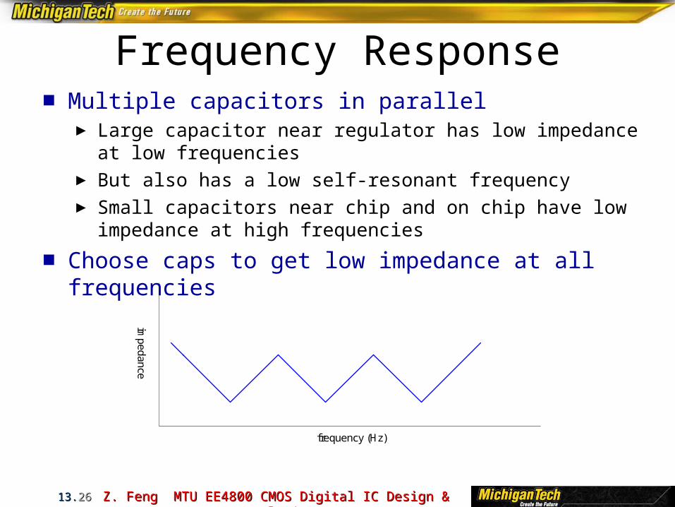
Frequency Response■ Multiple capacitors in parallel
► Large capacitor near regulator has low impedance at low frequencies
► But also has a low self-resonant frequency► Small capacitors near chip and on chip have low impedance at
high frequencies
■ Choose caps to get low impedance at all frequencies
frequency (Hz)
impedance
Z. Feng MTU EE4800 CMOS Digital IC Design & Z. Feng MTU EE4800 CMOS Digital IC Design & AnalysisAnalysis
13.13.2727
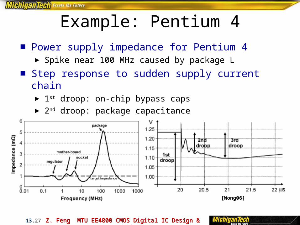
Example: Pentium 4■ Power supply impedance for Pentium 4
► Spike near 100 MHz caused by package L
■ Step response to sudden supply current chain► 1st droop: on-chip bypass caps► 2nd droop: package capacitance► 3rd droop: board capacitance
[Wong06]
Z. Feng MTU EE4800 CMOS Digital IC Design & Z. Feng MTU EE4800 CMOS Digital IC Design & AnalysisAnalysis
13.13.2828
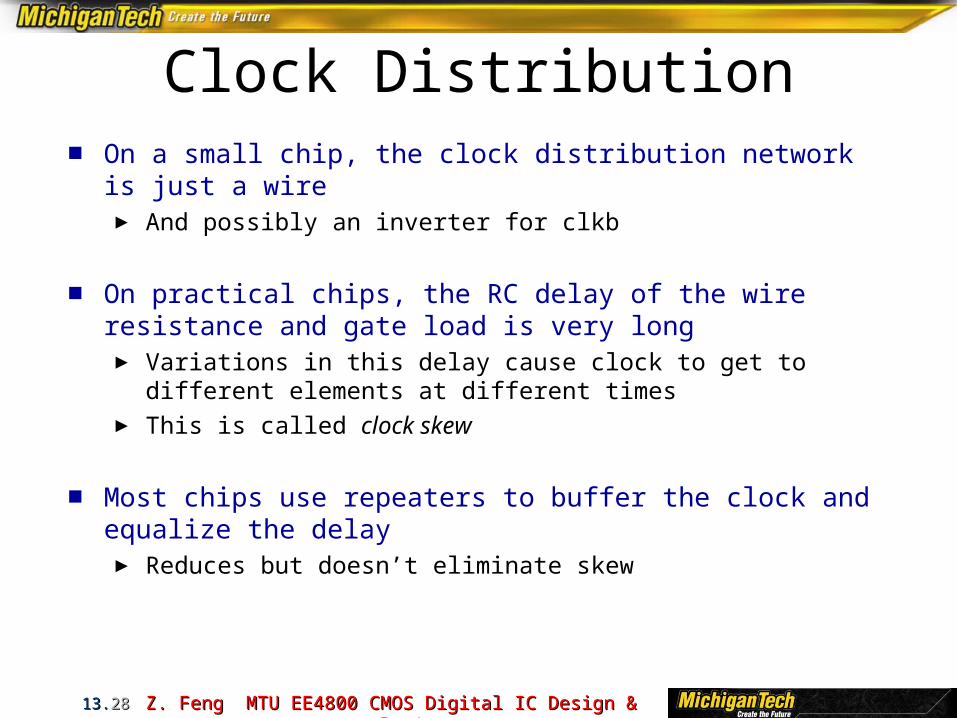
Clock Distribution■ On a small chip, the clock distribution network is just a
wire► And possibly an inverter for clkb
■ On practical chips, the RC delay of the wire resistance and gate load is very long
► Variations in this delay cause clock to get to different elements at different times
► This is called clock skew
■ Most chips use repeaters to buffer the clock and equalize the delay
► Reduces but doesn’t eliminate skew
Z. Feng MTU EE4800 CMOS Digital IC Design & Z. Feng MTU EE4800 CMOS Digital IC Design & AnalysisAnalysis
13.13.2929
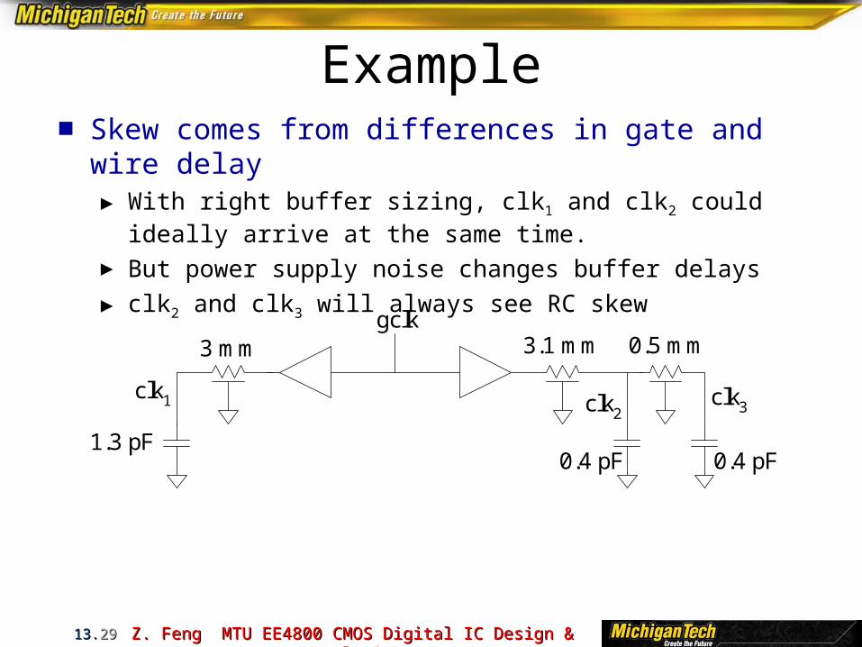
Example■ Skew comes from differences in gate and wire
delay► With right buffer sizing, clk1 and clk2 could ideally arrive at the
same time.► But power supply noise changes buffer delays
► clk2 and clk3 will always see RC skew
3 mm
1.3 pF
3.1 mmgclk
clk1
0.5 mm
clk2clk3
0.4 pF 0.4 pF
Z. Feng MTU EE4800 CMOS Digital IC Design & Z. Feng MTU EE4800 CMOS Digital IC Design & AnalysisAnalysis
13.13.3030
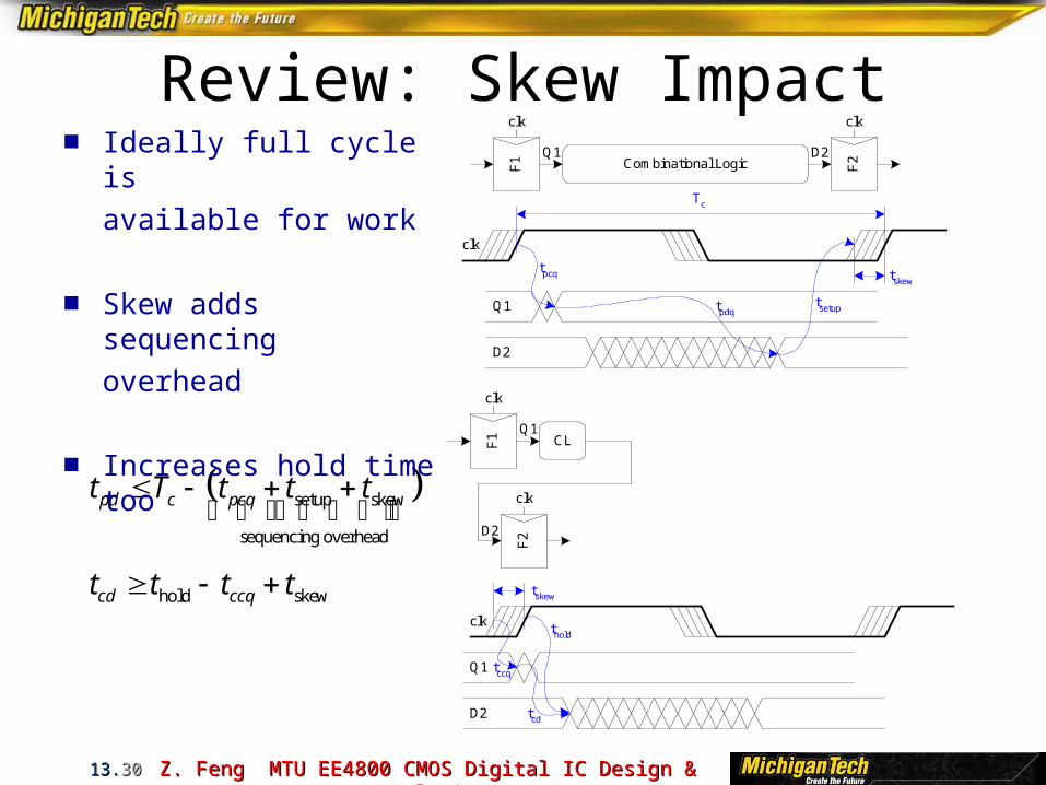
Review: Skew Impact
F1
F2
clk
clk clk
Combinational Logic
Tc
Q1 D2
Q1
D2
tskew
CL
Q1
D2
F1
clk
Q1
F2
clk
D2
clk
tskew
tsetup
tpcq
tpdq
tcd
thold
tccq
setup skew
sequencing overhead
hold skew
pd c pcq
cd ccq
t T t t t
t t t t
■ Ideally full cycle isavailable for work
■ Skew adds sequencingoverhead
■ Increases hold time too
Z. Feng MTU EE4800 CMOS Digital IC Design & Z. Feng MTU EE4800 CMOS Digital IC Design & AnalysisAnalysis
13.13.3131
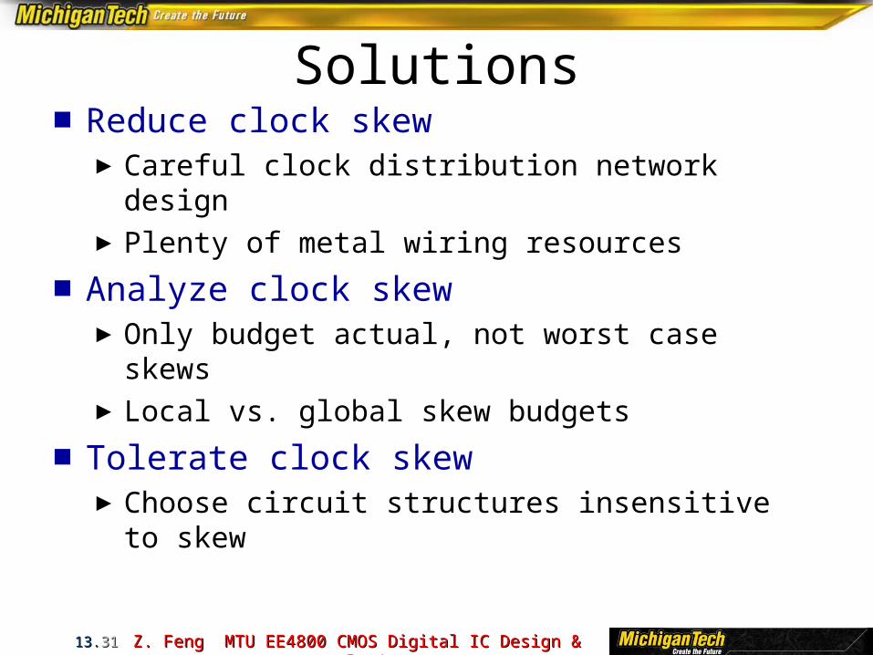
Solutions■Reduce clock skew
►Careful clock distribution network design►Plenty of metal wiring resources
■Analyze clock skew►Only budget actual, not worst case skews►Local vs. global skew budgets
■Tolerate clock skew►Choose circuit structures insensitive to skew
Z. Feng MTU EE4800 CMOS Digital IC Design & Z. Feng MTU EE4800 CMOS Digital IC Design & AnalysisAnalysis
13.13.3232
Clock Dist. Networks■Ad hoc■Grids■H-tree■Hybrid
Z. Feng MTU EE4800 CMOS Digital IC Design & Z. Feng MTU EE4800 CMOS Digital IC Design & AnalysisAnalysis
13.13.3333
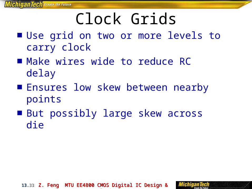
Clock Grids■Use grid on two or more levels to carry
clock■Make wires wide to reduce RC delay■Ensures low skew between nearby
points■But possibly large skew across die
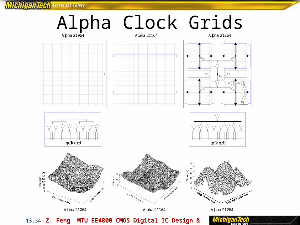
Z. Feng MTU EE4800 CMOS Digital IC Design & Z. Feng MTU EE4800 CMOS Digital IC Design & AnalysisAnalysis
13.13.3434
Alpha Clock Grids
PLL
gclk grid
Alpha 21064 Alpha 21164 Alpha 21264
gclk grid
Alpha 21064 Alpha 21164 Alpha 21264
Z. Feng MTU EE4800 CMOS Digital IC Design & Z. Feng MTU EE4800 CMOS Digital IC Design & AnalysisAnalysis
13.13.3535
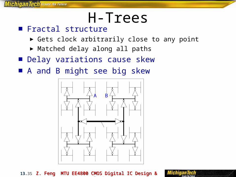
H-Trees■ Fractal structure
► Gets clock arbitrarily close to any point► Matched delay along all paths
■ Delay variations cause skew■ A and B might see big skew
A B
Z. Feng MTU EE4800 CMOS Digital IC Design & Z. Feng MTU EE4800 CMOS Digital IC Design & AnalysisAnalysis
13.13.3636
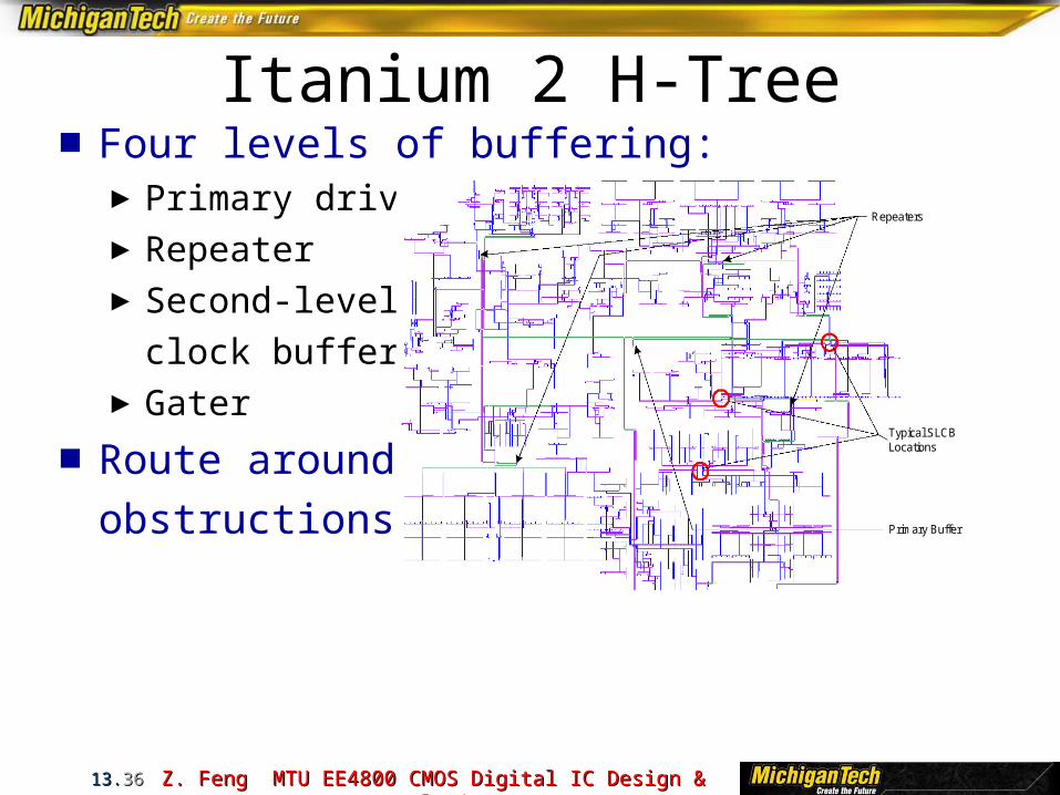
Itanium 2 H-Tree■Four levels of buffering:
►Primary driver►Repeater►Second-level
clock buffer►Gater
■Route aroundobstructions Primary Buffer
Repeaters
Typical SLCBLocations

Z. Feng MTU EE4800 CMOS Digital IC Design & Z. Feng MTU EE4800 CMOS Digital IC Design & AnalysisAnalysis
13.13.3737
Hybrid Networks■ Use H-tree to distribute clock to many points■ Tie these points together with a grid
■ Ex: IBM Power4, PowerPC► H-tree drives 16-64 sector buffers► Buffers drive total of 1024 points► All points shorted together with grid