ISSN 2395-1680 (ONLINE) ICTACT JOURNAL ON MICROELECTRONICS, JULY 2015, VOLUME: 01, ISSUE: 02
45
A NOVEL MIFGMOS TRANSISTOR BASED APPROACH FOR THE REALIZATION
OF TERNARY GATES
S. S. Narkhede1, B. S. Chaudhari
2 and G. K. Kharate
3
1Department of Electronics and Telecommunication Engineering, Pune Institute of Computer Technology, India
E-mail: [email protected] 2Department of Electronics and Telecommunication Engineering, Maharashtra Institute of Technology, India
E-mail: [email protected] 3Department of Electronics and Telecommunication Engineering, Matoshri College of Engineering, India
E-mail: [email protected]
Abstract
Multi Valued Logic [MVL] has experienced major evolution in the
recent past due to several advantages offered by them over the binary
logic. Ternary Logic (a logic with radix 3 i.e. 3 logic states) is a
promising alternative to the binary logic making it a thrust area of
research. With the recent technological advancements, commercial
realization of ternary circuits is watched with keen interests thereby
attracting the attention of wide community of researchers to explore
the usability of various alternative devices for implementing ternary
circuits. This research proposes a novel hybrid approach based on
combination of MIFGMOS (Multi Input Floating Gate Metal Oxide
Semiconductor) transistor and conventional MOSFET for the
realization of the ternary gates. In a digital system, NOT, NAND and
NOR are of more importance as they are the building blocks of many
other complex logic and arithmetic circuits. In this paper, the designs
(based on hybrid combination of devices) of two input TNAND and
TNOR gates are detailed which along with MIFGMOS transistor
based T-inverter are further used to design TAND, TOR, TXOR and
TXNOR gates. An extensive simulation of all the designed gates is
carried out using TSPICE circuit simulator. The results demonstrate
expected functionality of the proposed hybrid gates and additionally
signify improvement in the performance parameters. The proposed
hybrid approach combines the virtues of both the devices which
facilitate the significant reduction in the circuit element count of the
ternary gates as compared to earlier reported methods.
Keywords:
Multi Valued Logic, Ternary Logic, Ternary Gates, MIFGMOS
Transistor
1. INTRODUCTION
Multi Valued Logic [MVL] has experienced major evolution
in the recent past due to several advantages offered by them over
the binary logic. An evident advantage of MVL representation
over binary is economy of digits. Other advantages include
reduced number of interconnections and reduced chip area that
in turn reduces chip delay. One of the main advantages of MVL
is that it reduces the number of required computation steps. The
number of address lines required to access the address content
can be reduced, i.e. hardware cost can be reduced and less
memory is required. It also offers better utilization of
transmission channels because of the higher information content
carried by each line and gives more efficient error detection and
correction codes [1]. Elena et al. describe MVL as painting a
picture having all possible colours available, as against binary
logic which includes just black and white. MVL displays a
phenomenon that is never seen in binary, where the only two
possible values are null and unity elements of Boolean algebra,
possessing very specific properties [2]. MVL therefore emerges
as a thrust area for further research.
The ternary logic or radix 3 is the special case of MVL with
three logic levels. It has been watched with keen interests to
overcome the challenges of binary logic and solve numerous
problems more efficiently. The researchers have proposed two
different ternary logic systems namely, balanced and unbalanced
logic system. Balanced system uses –VDD for logic 0, 0V for
logic 1 and + VDD for logic 2 and unbalanced system uses 0V
for logic 0, VDD/2 for logic 1 and, VDD for logic 2. To
represent a number in binary system, more digits are required as
compared to that of ternary. As a result, using ternary system,
many logical and arithmetic operations can be executed with
higher speed and smaller number of computation stages. It is
therefore obvious that the ternary is casting its applications in
the field of fuzzy logic, machine learning, artificial intelligence,
data mining, robotics, digital signal processing, digital control
systems and image processing. It is also reported to solve the
binary problems more efficiently [3].
Complementary Metal Oxide Semiconductor (CMOS) has
been the predominant technology of the past two decades to
implement ternary and other MVL systems. Several types of
CMOS-based MVL circuits have already been proposed in the
literature as the emerging of MOSFET technology. However,
they are unsuitable for the current and the upcoming
technologies [3]. This encouraged the introduction of some
beyond-CMOS nano devices such as Carbon NanoTube Field
Effect Transistor (CNTFET)[3,4], Quantum-dot Cellular
Automata (QCA), Single Electron Technology (SET)[3] and
Quantum Dot Gate FET (QDGFET) [5] for MVL systems.
These nano devices benefit from low-power consumption,
ballistic transport attributes under low supply voltages and very
small sizes that make them very suitable for ultra-low-power,
ultra-high-performance and ultra-high-density chip design [3].
They are considered as a promising choice for future computing
technology in many areas including MVL. The present research
interests are therefore focused on investigating the utility of such
devices for designing ternary systems.
The proposed research aims to explore the usefulness of
MIFGMOS transistor for the design and simulation of ternary
logic gates. The device is composed of a floating gate and
calculates the weighted sum of the input. It is similar to
MOSFET in terms of inherent electronic characteristics. On
account of this similarity, previously designed structures based
on CMOS platforms can still be utilized in MIFGMOS transistor
based design. Standard Ternary Inverter [STI] is designed using
DOI: 10.21917/ijme.2015.0009

S S NARKHEDE et al.: A NOVEL MIFGMOS TRANSISTOR BASED APPROACH FOR THE REALIZATION OF TERNARY GATES
46
only MIFGMOS transistor and a novel hybrid approach based on
MIFGMOS transistor and conventional MOS transistor is
proposed for designing ternary universal gates with significant
reduction in the circuit element count and better performance
parameters. The obtained simulation results validate the
significance and the effectiveness of the proposed hybrid
approach as a potentially better technique from ternary
prospective.
The next section presents the structure and the modelling
equations of MIFGMOS transistor. Its advantages from Ternary
prospective are also discussed. Section 3 presents a brief review
of MVL and the advancements in its realizations. Section 4
details the proposed novel approach based on MIFGMOS
transistor and conventional MOS transistor to implement the
ternary universal gates. It must be noted that other Ternary gates
can further be designed using the TNAND and TNOR gates. The
simulation results are illustrated in section 5, which also include
rigorous timing analysis and analysis of Power Delay Product
[PDP]. The paper concludes with discussion and conclusion.
2. MIFGMOS TRANSISTOR
2.1 STRUCTURE OF MIFGMOS TRANSISTOR
A new functional MOS transistor has been proposed which
works more intelligently than a mere switching device. The
functional transistor calculates weighted sum of all input signals
at the gate level, and controls the “ON” and “OFF” state of the
transistor based on the result of such a weighted sum operation.
The function is quite analogous to that of biological neurons.
The device is composed of a floating gate and multiples of input
gates that are capacitively interacting with the floating gate. As
the gate-level sum operation is performed in a voltage mode
utilizing the capacitive coupling effect, essentially no power
dissipation occurs in the calculation, making the device ideal for
ULSI implementation. The structure of the MIFGMOS transistor
is depicted in Fig.1. [6]. They have the same basic properties as
equivalent ordinary MOS transistors but widened by certain
additional features. The most significant of them, there is the
ability of summing gate controlling input signals as well as the
possibility of reduction of threshold value voltage Vth
[6].
n
i i
n
i iiii
FF
C
VCtVCt
0
10
0
(1)
where
n is the number of inputs
F(t) is the potential at the floating gate.
Let Vth
be the threshold voltage of the transistor. Then the
transistor turns on at the condition F >Vth
, and is described by
the following Eq.(2) [6].
th
n
nn VCCCC
CVCVCV
021
2211
(2)
These transistors can operate as normal MOS as saturated or
non-saturated within the region of strong inversion or typically
within the region of weak inversion called sub-threshold region.
That second operating region is utilized in electronic circuits
with very low supply voltage [7].
The Fig.2 shows the output IV characteristics of n channel
and p channel MIFGMOS transistor operated under identical
voltage levels i.e. 5V, which confirm the design considerations
of the proposed approach. Eq.(3), Eq.(4) and Eq.(5) represent the
modelling equations of the MIFGMOS transistor [6].
Fig.1. Structure of MIFGMOS Transistor
(a)
(b)
Fig.2. IV characteristics of (a) nMIFGMOS transistor (b)
pMIFGMOS transistor
Cut off region
TGS
D
VV
I
0 (3)
Strong Inversion Ohmic region

ISSN 2395-1680 (ONLINE) ICTACT JOURNAL ON MICROELECTRONICS, JULY 2015, VOLUME: 01, ISSUE: 02
47
TGS
N
i
TT
FGBS
T
GBDS
T
GDiS
T
iDS
DST
GD
N
i T
FGBS
T
GBTiS
T
i
D
VV
VC
QV
C
CV
C
CV
C
CV
VC
C
C
QV
C
CVV
C
C
I
0
1
0
for
2
12
(4)
Strong Inversion Saturation region
TBS
DS
N
i
TT
FGBS
T
GBDS
T
GDiS
T
i
N
i
TT
FGBS
T
GBDS
T
GDiS
T
iD
VV
VVC
QV
C
CV
C
CV
C
C
VC
QV
C
CV
C
CV
C
CI
1
2
1
0
for
2
(5)
As clear from the characteristics and the modelling equation,
the three operating region of MIFGMOS transistor are cut off,
strong inversion ohmic and strong inversion saturation. In cut-
off region, gate to source voltage, Vgs is less than the threshold
voltage Vth
and no current flows through the device making it act
like a open switch. Whereas in strong inversion ohmic region,
Vgs is greater the Vth
and the device behaves like a resistor. In
strong inversion saturation region, the device is fully ON and
behaves as closed switch.
2.2 A BRIEF REVIEW OF MIFGMOS
TRANSISTOR
With the increasing demand for smaller and faster products,
there is an ongoing trend in fabrication process towards smaller
transistors. In the quest to achieve low-voltage and low-power,
various techniques have evolved in due course of time and
MIFGMOS transistor technique is one amongst them [8]. Due to
the special characteristics of the MIFGMOS transistor, its
application in both analog and digital circuits has been very wide
since the first report in 1967. The first well-known application of
the MIFGMOS was to store data in EEPROMs, EPROMs and
FLASH memories. During the last ten years, a number of
different applications have revealed possibilities that this device
could have in many other different fields [6]. Abhinav et al.
designed a new current mirror with MIFGMOS which exhibit
high output impedance, higher current range, very low power
dissipation and higher matching accuracy [8], [9]
A number of interesting applications have also been
exploited in digital circuits. It is demonstrated that a MOSFET
having an externally adjustable threshold voltage is quite
essential for implementing a MVL [10]. Other advantages listed
below also make MIFGMOS transistor a competent candidate
for the realization of ternary logic [6], [8].
From the implementation point of view, MVL designs must
be compatible with the existing binary technologies. MIFG MOS
transistors can be very well implemented in lieu of conventional
MOSFET.
Incredible features of flexibility, controllability and
tunability of MIFGMOS transistor yields better results with
respect to power, supply voltage and output swing.
A control voltage present at the MIFGMOS transistor and
facility of additional weighted inputs provides wide range of
tunability to the circuit.
Implementation of MIFGMOS transistor allows threshold
voltage (Vth
) controllability without reducing the feature size.
Also, it consumes less power than the minimum required power
for a circuit designed with conventional MOSFET.
Simplifies the topology of the digital systems (circuit
element count reduction)
For digital circuits, MIFGMOS transistor has thus been
considered to be a potentially better technique than standard
static CMOS Circuits [11].
In a digital system, NOT, NAND and NOR are of more
importance as they are the building blocks of many other
complex logic and arithmetic circuits. In this paper, the designs
(based on hybrid combination of devices) of two input TNAND
and TNOR gates are detailed which along with MIFGMOS
transistor based T-inverter are further used to design TAND,
TOR, TXOR and TXNOR gates.
3. RELATED LITERATURE
Alexender claimed that most efficient radix for
implementation of switching systems is natural base (e =
2.71828), where e is the Euler‟s constant. The base r = e2 =
7.38905609 with digits 0 and 1 only, was considered to be more
advantageous and most often used in electronic computers until
20th century. The 20th century however, brought a focus on
MVL ternary radix r = e3 = 20.08553692. The radix 3 number
system is known as Ternary Logic. As the value of radix
increases, the information carrying capacity of each connection
also increases. Hence, MVL, for instance, a3 valued (radix 3)
digital realization would be more appropriate than binary [12].
For instance, the third logic value for testing the binary
circuits can be used as a medium for signalling the faulty
operation [13]
Let us consider an m-valued function F(X) with k variables,
where X = {X1, X2, X3, …, Xk} and each xi can adopt values from
M = {0, 1, 2, …, m − 1}. Therefore the function F(X) is a
mapping f :Mk→M and consequently there are kmm different
functions possible in the set f. However, among these possible
functions, NOT, NAND and NOR operations seem to be more
important as they are the building blocks of many other complex
logical and arithmetic circuits. These fundamental logical
functions can be defined in an m-valued k-variable system
according to Eq.(6), Eq.(7) and Eq.(8) [3]
ama 1TNOT
(6)
kk aaamaaa ,,,min1,,,TNAND 2121
(7)
kk aaamaaa ,,,max1,,,TNOR 2121
(8)
S S NARKHEDE et al.: A NOVEL MIFGMOS TRANSISTOR BASED APPROACH FOR THE REALIZATION OF TERNARY GATES
48
The ternary logic is a common MVL, which includes three
significant logic levels. These logic levels can be considered as
„0‟, „1‟ and „2‟ symbols, which are counterpart to 0, ½VDD and
VDD voltage levels. Three different types of logics are defined
for the ternary logic, that is, negative, standard and positive such
as Negative Ternary Inverter (NTI), Standard Ternary Inverter
(STI) and Positive Ternary Inverter (PTI). The symbols of the
standard ternary gates are shown in Fig.1.
STI STNAND STNOR STAND STOR
Fig.3. Symbol of Ternary Gates
With the recent technological advancements commercial
realization of MVL circuits is watched with keen interest and is
a thrust area of research. Several types of CMOS- based MVL
circuits have already been proposed in the literature as the
emerging of MOSFET technology. However, they suffer from
many drawbacks which make them unsuitable for the current
and the upcoming technologies. Some of the reported
disadvantages are high static power, requirement of large off-
chip resistors, need of multiple supply voltages and use
depletion-mode MOSFETs that have become obsolete. [3].
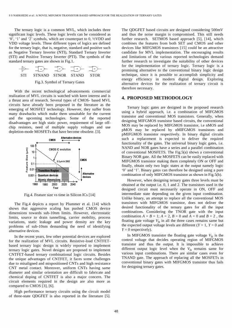
Fig.4. Feature size vs time in Silicon ICs [14]
The Fig.4 depicts a report by Plummer et al. [14] which
shows that aggressive scaling has pushed CMOS device
dimensions towards sub-10nm limits. However, electrostatic
limits, source to drain tunnelling, carrier mobility, process
variations, static leakage and power density are the key
problems of sub-10nm demanding the need of identifying
alternative devices.
In the recent years, few other potential devices are explored
for the realization of MVL circuits. Resistive-load CNTFET-
based ternary logic design is widely reported to implement
ternary logic gates. Novel designs are proposed to implement
CNTFET-based ternary combinational logic circuits. Besides
the unique advantages of CNTFET, it faces some challenges
due to misaligned and mispositioned CNTs and high resistance
CNT metal contact. Moreover, uniform CNTs having same
diameter and similar orientation are difficult to fabricate and
chemical doping of CNTFET is also a major concern. The
circuit elements required in the design are also more as
compared to CMOS [3], [6].
High performance ternary circuits using the circuit model
of three-state QDGFET is also reported in the literature [5].
The QDGFET based circuits are designed considering 500mV
and thus the noise margin is compromised. This still needs
further research. SETMOS based approach [5], [14], which
combines the features from both SET and CMOS and other
devices like MIFGMOS transistors [15] could be an attractive
candidate for MVL implementation. The encouraging results
and limitations of the various reported technologies demand
further research to investigate the suitability of other devices
for the implementation of ternary logic. Ternary logic is a
promising alternative to the conventional binary logic design
technique, since it is possible to accomplish simplicity and
energy efficiency in modern digital design. Exploring
alternative devices for the realization of ternary circuit is
therefore necessary.
4. PROPOSED METHODOLOGY
Ternary logic gates are designed in the proposed research
using a hybrid approach, i.e. a combination of MIFGMOS
transistor and conventional MOS transistors. Generally, when
designing MIFGMOS transistor based circuits, the conventional
MOS may be replaced by MIFGMOS transistor, i.e nMOS and
pMOS may be replaced by nMIFGMOS transistors and
pMIFGMOS transistor respectively. In binary digital circuits
such a replacement is expected to deliver the required
functionality of the gates. The universal binary logic gates, i.e.
NAND and NOR gates have a series and a parallel combination
of conventional MOSFETS. The Fig.5(a) shows a conventional
Binary NOR gate. All the MOSFETS can be easily replaced with
MIFGMOS transistor making them completely ON or OFF and
finally, obtain only two logic states at the output namely logic
„0‟ and „1‟. Binary gates can therefore be designed using a pure
combination of only MIFGMOS transistor as shown in Fig.5(b).
However, when designing ternary gates three levels must be
obtained at the output i.e. 0, 1 and 2. The transistors used in the
designed circuit must necessarily operate in ON, OFF and
intermediate state depending on the given input combination.
Unlike binary, an attempt to replace all the conventional MOS
transistors with MIFGMOS transistor, does not deliver the
desired functionality of the ternary gates for all the input
combinations. Considering the TNOR gate with the input
combination A = B = 1; A = 2, B = 0 and A = 0 and B = 2 , the
floating gate voltage Vfg in all the three cases remains same but
the expected output voltage levels are different (Y = 1, Y = 0 and
Y = 0 respectively).
In MIFGMOS transistor the floating gate voltage Vfg is the
control voltage that decides operating region of MIFGMOS
transistor and thus the output. It is impossible to achieve
different output logic level when the Vfg remains same for
various input combinations. There are similar cases even for
TNAND gate. The approach of replacing all the MOSFETs in
conventional binary gates with MIFGMOS transistor thus fails
for designing ternary gates.

ISSN 2395-1680 (ONLINE) ICTACT JOURNAL ON MICROELECTRONICS, JULY 2015, VOLUME: 01, ISSUE: 02
49
(a) (b)
(c) (d)
Fig.5. (a) Conventional NOR (b) All MOSFETs are replaced by
MIFGMOS transistor (c) The series combination of pMOSFETs
is replaced by single pMIFGMOS transistor (d) The parallel
combination of nMOSFETs is replaced by single nMIFGMOS
transistor
Assuming that the series combination of M1 and M2 in NOR
gate is replaced by a single MIFGMOS transistor, having two
inputs A and B connected to its floating gate as shown in
Fig.5(c). Considering ternary input combination, where A = 2
and B = 1 or vice versa demands output Y to be at logic „1‟.
Thus, the MIFGMOS transistor must necessarily operate in
intermediate state i.e. strong inversion ohmic state. However,
when the input A = 2 and B = 1, the floating gate voltage, Vfg is
sufficiently high to drive MIFGMOS transistor in strong
inversion saturation region and make it fully ON. One of the
MOSFETs in the parallel arm having logic „2‟ at its input is also
fully ON and thus shorts the VDD to ground. In such a situation
the output Y will obviously be pulled down to 0V. This design
therefore completely abolishes the occurrence of intermediate
state (level „1‟), at the output of the ternary gates. It is necessary
to restrict the MIFGMOS transistor to strong inversion ohmic
region and make it behave like resistor so as to obtain the output
as logic „1‟. The approach of replacing series combination of
MOSFETs with MIFGMOS transistor is highly undesired from
ternary prospective.
Thus when designing the MIFGMOS transistor based ternary
logic gates, a hybrid approach comprising of MIFGMOS
transistor and conventional MOSFET is inevitable. MOSFETs in
the series combination of NAND and NOR gates must
necessarily be retained and the use of MIFGMOS transistor must
be exploited in the parallel combination in the circuits as clearly
indicated in Fig.5(d). The ternary gates designed using this
approach is detailed in the next section.
5. SIMULATION RESULTS
The structure development using MIFGMOS transistor
requires validation and performance using simulators like
TSPICE. As the model parameters for MIFGMOS transistor are
not available, hence standard MOS models are used to simulate
these structures. The electrical components are added to the
standard MOS models to emulate the MIFGMOS transistor
behaviour. The equivalent circuit of MIFGMOS transistor
contains various capacitors. When this circuit is simulated using
TSPICE, the problem of floating nodes arises, as a result the
simulations fail to converge. As TSPICE cannot accept floating
nodes having no dc path to ground, we need to bypass each
capacitor with a resistor.
5.1 TERNARY INVERTER
The Yoeli-Rosinfeld algebra defines three basic ternary
elements, the Standard Ternary Inverter [STI], Positive Ternary
Inverter [PTI] & Negative Ternary Inverter [NTI] such that,
iXi
iXii
i
X
XX
2NTIPTI,
2STI
(9)
where „i‟ take the value of „2‟ for PTI & „0‟ for NTI inverter [16].
Table.1. Truth table of STI, PTI & NTI
A STI PTI NTI
0 2 2 2
1 1 2 0
2 0 0 0
Table.2. Model simulation parameters and node voltages of the
proposed MIFGMOS transistor based STI circuit.
Input
‘A’
T1
pMIFG
(W = 16µm, L =
120nm)
Vt = -0.75V
T2
nMIFG
(W= 8m,
L = 120nm )
Vt = 0.65V
O/P
‘Y’
Ternary
logic
level
Vfg Vgs1 Vfg Vgs2
0 (0V) 0V -5V 0 0 5V 2
1 (2.5V) 2.5V -2.5V 2.5V 2.5V 2.5V 1
2 (5V) 4.78V 0V 4.78V 4.78V 0V 0
The truth table for the Ternary Inverters, STI, PTI and NTI is
given in Table.1. The Fig.6(a) represents the proposed
MIFGMOS transistor based STI circuit. The proposed circuit is
same as the conventional CMOS inverter, except that the
transistors have been replaced by MIFGMOS transistor. As
depicted in Fig. 6(a) the chosen values of C1, C2 and C3 are 10fF,
210fF and 10fF respectively. Eq.(1) of Vfg becomes
TFG
C
VCVCVCV 332211
(10)
Vfg represent the voltage at the floating gate, which is
common to both the transistors in the proposed STI. Table.2
details the operational voltages of the MIFGMOS transistor

S S NARKHEDE et al.: A NOVEL MIFGMOS TRANSISTOR BASED APPROACH FOR THE REALIZATION OF TERNARY GATES
50
based STI. As illustrated, using Eq.(10) the calculated values of
Vfg for logic 0, 1 and 2 are 0 V, 2.5V and 4.78V. The threshold
voltage of the designed gate is -0.75V and 0.65V for M1 and M2
respectively.
(a)
(b)
Fig.6. (a) Proposed MIFGMOS transistor based STI (b) input
and output waveform of STI
Fig.7. VTC of STI
Table.3. Noise Margin of STI
NM0 0.60V
1NM 0.92V
1NM 0.73V
NM2 0.93V
When the input „A‟ is at logic „0‟, transistor M1 is operating
in strong inversion saturation i.e. ON state. However, no
inversion layer is formed in transistor, M2 thereby forcing it to
be in OFF state and making the output Y to be at logic „2‟.
Similarly when the input „A‟ is at logic „2‟, the Vfg is greater than
Vth
= 0.65, making it operate in strong inversion saturation and
thus turning it ON. Transistor M1 is OFF, bringing the output Y,
at logic „0‟, thus inverting the input as per the truth table of STI.
Logic „1‟ at the input A, drives the transistors to operate in the
intermediate state, thus making both of them behave like a
resistor. In such situation, the circuit behaves like a voltage
divider, producing the output of VDD/2, i.e. 2.5V (Logic 1) at
the output. The Fig.6(b) illustrates the simulation results of the
proposed MIFG based STI that conform with the input output
conditions described in Table.1.
Table.4. Comparison of transition
Transition
logic to
logic
Rise / Fall time
[17]
Bala P C
et. al.
[5]
Supriya
et. al.
Proposed
approach
1-2 12ns 11.18ps 5.09ps
2-1 12ns 11.18ps 5.20ps
1-0 20ns 11.18ps 6.84ps
0-1 20ns 11.18ps 4.54ps
2-0 20ns 13.43ps 10.43ps
0-2 20ns 13.41ps 10.43ps
Extensive performance analysis of the proposed STI is
performed and the obtained results for the Noise Margin and
Rise/Fall time are summarized in the Table.3 and Table.4
respectively. The Fig.7 depicts the Voltage Transfer Curve
[VTC] of the STI. Three states corresponding to logic level 0, 1
and 2 are clearly seen.
Ternary logic has four different noise margins as described in
[18]. The obtained VTC curve is used to further calculate the
noise margins. The calculated noise margin for the proposed STI
are detailed in Table.3. As indicated in Table.3, the transition
time of the MIFGMOS transistor based STI is less than the other
reported approaches in [5], [15]. The comparison with the state
of art methods as detailed in Table.4 showcases the effectiveness
and advantages of replacing the conventional MOSFET inverter
with the proposed MIFGMOS based STI.
5.2 TERNARY NAND
The TNAND gate can be defined as,
nn XXXXXX 2121 ,min,TNAND
(11)
The sign „.‟ indicates logical ternary AND operation. The
Ternary NAND gate can be configured as Standard Ternary
NAND [STNAND], Positive Ternary NAND [PTNAND] and
Negative Ternary NAND [NTNAND] [16]. The Table.5
represents the truth table of the TNAND gate.
The Fig.8(a) represents the proposed MIFG based STNAND
circuit. The conventional binary CMOS based NAND circuit is
modified by replacing the parallel combination of pMOS by a
single pMIFG. The nMOS in the series arm of the binary NAND
are retained in the proposed design of the ternary gates. The
proposed MIFG based design thus reflects a novel hybrid
combination of the circuit elements to achieve the functionality
of the ternary STNAND gate.
As depicted in Fig.8(a) the chosen values of C1, C2 and C3
are 210fF, 210fF and 10fF respectively. The differential voltage
between floating gate and the source terminal of MIFG decides

ISSN 2395-1680 (ONLINE) ICTACT JOURNAL ON MICROELECTRONICS, JULY 2015, VOLUME: 01, ISSUE: 02
51
the state of operation of pMIFG. The threshold voltage, Vth
of M3
is -0.65V and Vth
of M2 and M1 is 1.3V and 0.85V respectively.
A = B = 0
When both the inputs A and B of the designed Ternary gate
are logic „0‟, the transistor M3, i.e. pMIFG is completely ON and
is operating in the strong inversion saturation. The nMoS in the
series arm that receives logic state „0‟ input is in OFF state thus
bringing the output Y at logic „2‟.
(a)
(b)
Fig.8. (a) Proposed Ternary NAND (b) input and output
waveform of T-NAND
Table.5. Truth Table of Ternary NAND gate
A B Y
0 0 2
0 1 2
0 2 2
1 0 2
1 1 1
1 2 1
2 0 2
2 1 1
2 2 0
Fig.9. PDP of TNAND for different capacitive load and
frequencies
A = B = 2
When both the inputs, A and B are at logic „2‟ the pMIFG
(M3) is in OFF state. The nMOS transistors, M1 and M2 are
operating in strong inversion saturation. So the output Y is pulled
to logic „0‟.
A = 1, B = 1; A = 1, B = 2; A = 2, B = 1
When one of the inputs to the ternary STNAND is at logic
„1‟ and if the other input is either at logic „1‟ or „2‟, in such a
case the output Y is at logic „1‟.
In all above cases the pMIFG operates in strong inversion
ohmic When one of the inputs is at logic „2‟, the corresponding
nMOSFET is fully ON and driven into strong inversion
saturation region. The remaining nMOSFET and pMIFG
operates in strong inversion ohmic region and forms a voltage
divider circuit to deliver output at logic „1‟.
The nMOSFET having input logic „0‟ is in cut-off state
thereby making the rail to rail Id drop to zero. The sourcing
current of pMIFGMOS transistor in such a situation is less as
compared to its sourcing current when the output Y is at logic „2‟.
As already discussed in section 4, the floating gate voltage,
Vfg in last cases (A = 0, B = 2 and A = B = 1) is same for both the
cases but the expected logic level at the output is different (Y = 2
and Y = 1 respectively). The proposed hybrid approach of using
a combination of both the devices, MIFG and MOSFET has
addressed the issue and has delivered good results for all the
combination of inputs.
The Fig.8(b) illustrates the simulation results for all the input
combinations. The voltage levels at Vfg are also depicted in the
figure. The output voltage Y confirms the functionality of the
designed gates. The Power Delay Product (PDP) of the proposed
gate for various frequencies (500 KHz to 5 MHz) and various
loads (1pF to 10pF) is shown in Fig.9. As expected the PDP
increases with increase in load.
5.3 TERNARY NOR
Ternary NOR has an output that is a compliment of OR
function i.e.
nn XXXMaxXXX ...,.......TNOR 2121 (12)
0.00E+00
5.00E-12
1.00E-11
1.50E-11
2.00E-11
2.50E-11
3.00E-11
PD
P(J
)
555K
1.11M
5.55M

S S NARKHEDE et al.: A NOVEL MIFGMOS TRANSISTOR BASED APPROACH FOR THE REALIZATION OF TERNARY GATES
52
The sign „+‟ indicates logical ternary OR operation. The
Ternary NOR gate can be configured as Standard Ternary NOR
[STNOR], Positive Ternary NOR [PTNOR] and Negative
Ternary NOR [NTNOR] [16]. The Table.6 represents the truth
table of the TNOR gate.
The Fig.10(a) represents the proposed MIFG based STNOR
circuit. The conventional binary CMOS based NOR circuit is
modified by replacing the parallel combination of nMOS by a
single nMIFG, M3. The two pMOS in the series arm of the
conventional binary NOR are retained in the proposed design of
the ternary gates as M1 and M2. The proposed MIFG based
design thus reflects a novel hybrid combination of the circuit
elements to achieve the functionality of the ternary STNAND
gate.
As depicted in Fig.10(a) the chosen values of C1, C2 and C3
are 100fF, 100fF and 10fF respectively. The differential voltage
between floating gate and the source terminal of MIFG decides
the state of operation of nMIFG. The threshold voltage, Vth
of M3
is 0.8V and Vth
of both, M2 and M1 is -0.8V.
Table.6. Truth Table of Ternary NOR Gate
A B Y
0 0 2
0 1 1
0 2 0
1 0 1
1 1 1
1 2 0
2 0 0
2 1 0
2 2 0
(a)
(b)
Fig.10. (a) Proposed Ternary NOR (b) input and output
waveform of T-NOR
Fig.11. PDP product of TNOR for different capacitive load and
frequencies
A = B = 0
When both the inputs are „0‟, M3 is OFF and both M1 and M2
are ON and operates in strong inversion saturation, providing
path to Vdd. Logic level of „2‟ is obtained at the output Y.
A = 1, B = 0; A = 0, B = 1
When one of the inputs, A or B is at logic „1‟ and the other
input is either „0‟ or „1‟, the transistor M3 is at strong inversion
ohmic region. The transistor (M1 or M2) receiving logic level „1‟
at its input operates in strong inversion ohmic region. The
MOSFET receiving logic „0‟ is completely ON and operates in
strong inversion saturation region. The circuit behaves as voltage
divider and produces an output of VDD/2 i.e logic „1‟ at Y.
A = 2, B = 1; A = 1, B = 2; A = B = 2
The floating gate voltage obtained because of above
combinations is different but the expected output for all is Y= 0
for all of them. When one of the inputs is at logic „2‟, the
pMIFG is driven into strong inversion saturation region and
pMOSFETs that receives logic „2‟ at its input is in cut-off state,
thereby disconnecting the path from VDD to output and thus
forcing Y to be at logic „0‟.
A = 1, B = 1; A = 2, B = 0; A = 0, B = 2;
In above three cases, the floating gate voltage, Vfg, obtained
due to these input combinations is same but the expected logic
level at the output is different (Y = 1, Y = 0 and Y = 0
respectively). When both the inputs A = B = 1, all the transistors
0.00E+00
5.00E-12
1.00E-11
1.50E-11
2.00E-11
PD
P(J
)
555K
1.11M
5.55M

ISSN 2395-1680 (ONLINE) ICTACT JOURNAL ON MICROELECTRONICS, JULY 2015, VOLUME: 01, ISSUE: 02
53
operate in saturation inversion ohmic region and function as
voltage divider to deliver an output of logic „1‟. On the contrary,
in remaining two combinations of inputs, M3 operates in strong
inversion ohmic region and as already detailed in above case (case
iii) , the output Y, is pulled down to logic „0‟ because one of the
pMOSFET operates in cut-off region. The sinking current of
nMIFGMOS transistor in such a situation is less as compared to
its sinking current when the output Y is at logic „0‟. This condition
decides the maximum fan out for the proposed TNOR gate.
The Fig.10(b) illustrates the simulation results for all the
input combinations. The voltage levels at Vfg are also depicted in
the figure. The output voltage Y confirms the functionality of the
designed gates. The PDP of the proposed gate for various
frequencies (500KHz to 5MHz) and various loads (1pF to 10pF)
is shown in Fig.11. As expected the PDP increases with increase
in load. For a specific load, the PDP remains constant inspite of
large variations in frequency.
5.4 TERNARY AND
TAND gate is designed by inverting the outputs of ternary
NAND using STI. The Table.7 indicates the truth table of
TAND. The circuit diagram of the designed TAND is illustrated
in Fig.12(a). The simulated input-output waveform of the ternary
AND is shown in Fig.12(b). The PDP of the designed TAND is
also calculated and illustrated in Fig.13.
(a)
(b)
Fig.12. (a) Proposed Ternary AND (b) input and output
waveform of TOR
Table.7. Truth Table of Ternary AND and Ternary OR Gates
A B TAND TOR
0 0 0 0
0 1 0 1
0 2 0 2
1 0 0 1
1 1 1 1
1 2 1 2
2 0 0 2
2 1 1 2
2 2 2 2
Fig.13. PDP of TAND for different capacitive load and
frequencies
(a)
0.00E+00
5.00E-12
1.00E-11
1.50E-11
2.00E-11
PD
P(J
)
555K
1.11M
5.55M

S S NARKHEDE et al.: A NOVEL MIFGMOS TRANSISTOR BASED APPROACH FOR THE REALIZATION OF TERNARY GATES
54
(b)
Fig.14. (a) Proposed Ternary OR (b) input and output waveform
of TAND
Fig.15. PDP of TOR for different capacitive load and
frequencies
(a)
(b)
Fig.16. (a) Proposed Ternary EXOR and EXNOR (b) input and
output waveform of TEXOR and TEXNOR
5.5 TERNARY OR
Similar to TAND, TOR gate is designed by inverting the
output of TNOR gate. The circuit diagram of the designed
TAND is illustrated in Fig.14(a). The simulated input-output
waveform of the ternary AND is shown in Fig.14(b). The PDP
of the designed TAND is also calculated and illustrated in
Fig.15.
Table.8. Truth Table of Ternary XOR and Ternary XNOR Gates
A B TXOR
(Y)
TXNOR
(Y1)
0 0 0 2
0 1 1 1
0 2 2 0
1 0 1 1
1 1 1 1
1 2 1 1
2 0 2 0
2 1 1 1
2 2 0 2
5.6 TERNARY XOR AND TERNARY XNOR
TXOR and TXNOR functions can be implemented by
combining the STI, TAND, and TOR gates as indicated in
Fig.16. The output of TXOR, Y is further complemented to
obtain the output of TXNOR, Y1. The truth table of both the
gates is represented in Table.8. The simulated input-output
waveform of the ternary XOR and XNOR gate is shown in
Fig.16.
6. DISCUSSION AND CONCLUSION
This paper proposes a novel hybrid approach based on
MIFGMOS technology for the realization of the ternary gates.
The designs (based on hybrid combination of devices) of two
input TNAND and TNOR gates are detailed. The proposed
TNAND and TNOR gates along with MIFGMOS transistor
based T-inverter is further used to design TAND, TOR, TXOR
and TXNOR gates.
An extensive simulation of all the designed gates is carried
out using TSPICE circuit simulator. The results demonstrate
expected functionality of the proposed hybrid gates and an
additional improvement in the performance parameters is also
achieved.
The earlier reported CMOS technique for the implementation
of ternary gates uses an additional power supply and passive
components to obtain the intermediate state i.e. logic state „1‟
[3], [16]. This is because, in such circuits CMOS operates only
in ON and OFF states. The proposed novel approach however
eliminates the need of additional power supply and components
to achieve the intermediate state.
0.00E+00
5.00E-12
1.00E-11
1.50E-11
2.00E-11
2.50E-11
PD
P(J
)
555K
1.11M
5.55M

ISSN 2395-1680 (ONLINE) ICTACT JOURNAL ON MICROELECTRONICS, JULY 2015, VOLUME: 01, ISSUE: 02
55
Table.9. Comparison of number of circuit elements
Sl.
No.
Designed
Ternary
Circuits
CNTFET
[4]
Sheng L
et. al.
QDGFET
[ 5]
Supriya
K et. al.
Proposed
Hybrid
(MIFG-
MOS)
Approach
1. T-INV (STI) 06 03 02
2. T -NAND 10 04 03
3. T-NOR 10 04 03
4. T-AND 16 07 05
5. T-OR 16 07 05
The weighted sum of the input voltages at floating gate
provides the flexibility to drive the circuit in ON, OFF and
intermediate state (strong inversion ohmic). This is significant
improvement as compared to the earlier CMOS designs [3], [16],
[19].
A ternary processor will obviously have numerous
combinational and sequential circuits demanding multiple
inputs, multiple outputs, series and parallel architectures and
operations. Our further research aims to use the proposed ternary
gates as the fundamental block in designing such combinational
and sequential ternary circuits. It is therefore necessary to have
large values of fan in and fan out in the proposed ternary gates.
Jon et al. [11] analyses the floating gate circuits to suggest a
general rule of thumb that FGMOS circuits with sub-threshold
power supply should not be designed with a fan in larger than 3.
This will set limits to FGMOS circuits and many previous
proposed designs will not be helpful. The operating voltage in
the proposed hybrid approach is selected to be 5 V, which is
expected to provide a better fan in when further used in the
ternary combinational and sequential circuits. As indicated in the
PDP graphs (Fig.9, Fig.11, Fig.13 and Fig.15), the functionality
of the designed gates was verified for various frequencies
(500KHz to 5MHz) and various loads (1pF to 10pF). A direct
comparison of the PDP with the state of art methods may not
necessarily justify the effectiveness of the proposed approach.
This is because PDP is directly proportional to load capacitance,
frequency and VDD. The reported CNTFET [4] and QDGFET
[5] based methods use VDD of 900mV and 500mV respectively
and therefore cannot be directly compared with the proposed
approach. Nevertheless, the performance analysis of the
proposed ternary gates using PDP as a figure of merit to
determine its quality is merely indicative. Acceptable voltage
levels were obtained at the output for the variations in load
capacitance and frequency. This signifies good fan-out values of
the proposed ternary gates, which is an apparent advantage of
operating MIFGMOS transistors at 5V.
Another apparent advantage of using 5V as the operating
voltage is the higher noise margins. The literature reports the
noise margin of 50mV for the operating voltage of 500mV [5].
The noise margins of the proposed gates, as summarized in
Table.4, are quite higher than the reported values.
The Table.9 presents a comparison of the circuit elements
used by the researchers in the approaches devised by them. The
proposed hybrid approach has achieved good reduction in the
circuit element count. This reduction will further be more
significant when building ternary combinational and sequential
circuits.
The simulation results and the comparison Table.9 confirms
the authenticity of the proposed hybrid MIFGMOS transistor
based method as well as the superiority of the proposed ternary
circuits specifically in terms of the circuit element count and
performance parameters like PDP and rise/fall time in
comparison with the other state-of-the-art ternary circuits. Our
further research aims to explore other properties of MIFGMOS
transistor like tunabilty when designing ternary combinational
and sequential circuits.
REFERENCES
[1] X. W. Wu and F. Prosser, “CMOS Ternary Logic Circuits”,
IEEE Proceedings on Circuits, Devices And Systems,
Vol. 137, No. 1, pp. 21-27, 1990.
[2] Elena Dubrova, “Multi-Valued Logic in VLSI: Challenges
and Opportunities”, Proceedings of NORCHIP,
pp. 340-350, 1999.
[3] Mohammad H Moaiyeri, R.F. Mirzaee, Akbar
Doostaregan, Keivan Navi and Omid Hashemipour, “A
Universal Method for Designing Low-Power Carbon
Nanotube FET-Based Multiple-Valued Logic Circuits”,
IET Computers & Digital Techniques, Vol. 7, No. 4,
pp. 167-181, 2013.
[4] Sheng Lin, Yong Bin Kim and Fabrizio Lombardi,
“CNTFET Based Design of Ternary Logic Gates and
Arithmetic Circuits”, IEEE Transactions on
Nanotechnology, Vol. 10, No. 2, pp. 217- 225, 2011.
[5] Supriya Kamakar, John A. Chandy and F. C. Jain, “Design
of Ternary Logic Combinational circuits Based on
Quantum Dot Gate FETs”, IEEE Transactions on Very
Large Scale Integration (VLSI) Systems, Vol. 21, No. 5,
pp. 793-806, 2013.
[6] Ester Rodriguez-Villegas. “Low Power and Low Voltage
Circuit Design with the FGMOS Transistor”, Institution of
Engineers and Technology, 2006.
[7] K. Topor and P. Holajn, “Multiple-Input Floating-Gate
MOS Transistor in Analogue Electronics Circuit”, Bulletin
of the Polish Academy of Sciences Technical Sciences,
Vol. 52, No. 3, pp. 251-256, 2004.
[8] A. Anand, M.Sushanta, D. Anindita and B. Shivalal,
“FGMOS Based Low-Voltage Low-Power High Output
Impedance Regulated Cascode Current Mirror”,
International Journal of VLSI Design & Communication
Systems, Vol. 4, No. 2, pp. 39-50, 2013.
[9] J. de la Cruz Alejo and L. N. O. Moreno, “Mismatch
Compensation in Current Mirrors with FGMOS
Transistor”, 7th
International Conference on Electrical
Engineering Computing Science and Automatic Control,
pp. 599-603, 2010.
[10] Tadashi Shibata and Tadahir Ohmi, “A Functional MOS
Transistor Featuring Gate-Level Weighted Sum and
Threshold Operations”, IEEE Transactions on Electron
Devices, Vol. 39, No. 6, pp. 1444-1455, 1992.
[11] Jon Alfredsson, Aunet Snorre and Oelmann Bengt, “Small
Fan-in Floating-gate Circuits with Application to an
Improved Adder Structure”, 20th
International Conference
on VLSI design, pp. 314-317, 2007.
[12] Sakamoto Masahiro and Morisue Mititada, “A Study of
Ternary Fuzzy Processor using Neural Networks”, IEEE

S S NARKHEDE et al.: A NOVEL MIFGMOS TRANSISTOR BASED APPROACH FOR THE REALIZATION OF TERNARY GATES
56
International Symposium on circuits and systems, Vol. 1,
pp. 613-616, 1997.
[13] M. Serra, “Applications of Multi Valued Logic to Testing
of Binary and MVL Circuits”, International Journal of
Electronics, Vol. 63, No. 2, pp. 197-214, 1987.
[14] James D. Plummer and Peter B. Griffan, “Material and
Process limits in silicon VLSI technology”, Proceedings of
the IEEE, Vol. 89, No. 3, pp. 242-258, 2001.
[15] Wang, Samuel Tuan. “On the I-V characteristics of
floating-gate MOS transistors”, IEEE Transactions on
Electron Devices, Vol. 26, No. 9, pp. 1292-1294, 1992.
[16] A. P. Dhande, S. S Narkhede and S. S. Dudam, “VLSI
Implementation of Ternary gates using Tanner Tools”, 2nd
International conference on Devices, Circuits and Systems,
pp 1-5, 2014.
[17] P. C. Bala and A. Antoniou , “Low Power dissipation MOs
ternary logic family”, IEEE Journal of Solid State
Circuits, Vol. 19, No 5, pp. 739-749, 1984.
[18] A. Forster, “Resonant Tunnelling Diodes: The Effect Of
Structural Properties on Their Performance”, Advances In
Solid State Physics, Vol. 33, pp. 37-62, 1994.
[19] A. Srivasta, “Back Gate Bias Method of Threshold Voltage
Control for the design of Low Voltage CMOS Ternary
Logic Circuits”, Microelectronics Reliability, Vol. 40,
No. 12, pp 2107-2110, 2000.
Recommended