8/8/2019 An 8T Sub Threshold SRAM Cell Utilizing Reverse Short Channel
http://slidepdf.com/reader/full/an-8t-sub-threshold-sram-cell-utilizing-reverse-short-channel 1/4
An 8T Subthreshold SRAM Cell Utilizing Reverse Short Channel
Effect for Write Margin and Read Performance ImprovementTae-Hyoung Kim, Jason Liu and Chris H. Kim
Department of Electrical and Computer Engineering
University of Minnesota, Minneapolis, MN, USA
Abstract -We propose a technique for improving write margin and
read performance of 8T subthreshold SRAMs by using long
channel devices to utilize the pronounced reverse short channel
effect. Simulations show that the proposed cell at 0.2V has a write
margin equivalent to a conventional cell at 0.27V. The Ion-to-Ioff
ratio of the read path also improved from 169 to 271 and a 52%
speedup for read was achieved. The cell area overhead was 20%.
I. I NTRODUCTION Subthreshold logics are becoming increasingly popular for
ultra-low power applications such as portable electronics,medical instrumentations, and sensor networks where minimal power consumption is the primary design constraint [1][2].
Subthreshold logic can operate while consuming orders of
magnitude less power than in the normal strong-inversionregion. Characteristics of MOS transistors in the subthresholdregion are significantly different from those in the strong-inversion region. The MOS saturation current becomes anexponential function of the terminal voltages in this regime
leading to an exponential increase in MOS current variabilityunder Process-Voltage-Temperature (PVT) fluctuations.
Designing robust SRAM memories in the subthreshold regionis a particularly challenging task due to the small Ion-to-Ioff ratio and the increased current variability. Reduced readmargin, small write margin, and increased speed/power
variations are the main design challenges for subthresholdSRAMs.
SRAM read stability is already a problem in conventional6T cells in the strong inversion region as the access transistor can considerably raise the internal node voltage that stores a
‘0’ so as to trip the cell data. This problem worsens in thesubthreshold region as the current variability increases. Awidely used method for improving the Static Noise Margin
(SNM) in subthreshold SRAMs is decoupling the cell nodefrom bitline by using additional read path transistors [3][4].By doing so, the SNM in read mode becomes equal to that in
hold mode. The write margin problem is exacerbated insubthreshold due to the increased current sensitivity to PVTvariations. A higher wordline voltage was used in [4] to
strengthen the write path and overcome the impact of variations at the cost of additional power routing/generation
circuits and increased power consumption. Other previousmethods used a collapsed cell supply voltage during write
operation to weaken the strength of the pull up PMOS.This paper presents a new technique for improving the
write margin and read performance of 8T subthresholdSRAMs without requiring any additional supply voltage or
extra circuitry. We utilize the pronounced Reverse ShortChannel Effect (RSCE) [5][6][7] in the subthreshold region toincrease the strength of write access devices. By simply using
longer channel length access devices, the threshold voltage isreduced and the current drivability is improved due to the
exponential dependency of current on threshold voltage.Similarly, the read path delay and variation tolerance was also
improved by deploying longer channel length devices thatutilize the RSCE.
II. CONVENTIONAL 8T SRAM CELL
Fig. 1 shows the conventional 8T SRAM cell. It containsseparate read and write paths with respective wordline signalsWWL and RWL. Read port consists of two transistors (M7,
M8) and write port includes two transistors (M3, M6). Toimprove the read stability, cell nodes are decoupled from the
read bitline (RBL) via read devices M7 and M8. When readwordline (RWL) is enabled, the read bitline (RBL) isconditionally discharged based on the cell data. Because thecell nodes are decoupled from the RBL, this design maximizes
the read stability.
Figure 1. Conventional write margin improvement techniques for 8T SRAMs.
Write operation is executed by enabling the write wordline(WWL) after loading the data onto the write bitlines (WBL,WBLB). The current ratio between the write access transistors
(M3, M6) and the pull-up transistors (M2, M5) determines thecell write margin. If the strength of the write access transistor
is too weak to pull down the node voltage storing a ‘1’ close toGND, the write operation will fail. To prevent the writefailure, strong access transistors are needed to increase the
write path strength. However, in the subthreshold region,sizing alone cannot solve the write margin problem due to thelarge process variation and area overhead. Several techniques
have been proposed to improve the write margin. A higher wordline voltage has been applied to the write accesstransistors (M3, M6) to increase the current drivability [4].This improves the write margin at the cost of additional power
routing, extra voltage generation circuitry and increased power consumption. Another widely used method is collapsing the
cell supply voltage to weaken the strength of PMOS duringthe write operation. However, the collapsed supply voltage
deteriorates the stability of other SRAM cells which are notsupposed to be written but are connected to the same bitline or wordline. The cell stability is already close to the failure point
241
IEEE 2007 Custom Intergrated Circuits Conference (CICC)
1-4244-1623-X/07/$25.00 ©2007 IEEE MP-15-1

8/8/2019 An 8T Sub Threshold SRAM Cell Utilizing Reverse Short Channel
http://slidepdf.com/reader/full/an-8t-sub-threshold-sram-cell-utilizing-reverse-short-channel 2/4
in subthreshold SRAMs which makes the collapsed supplyvoltage scheme difficult to be used.
III. PROPOSED SUBTHRESHOLD SRAM CELL DESIGN
A. Impact of Reverse Short Channel Effect in Subthreshold
As process technology scales, V th roll-off caused by DrainInduced Barrier Lowering (DIBL) becomes stronger. To
compensate for the strong DIBL, non-uniform doping calledHALO implants is used in the source-body and drain-body boundaries to reduce the amount of control the drain has over the channel. However, as a byproduct of using HALO
implants, the threshold voltage decreases as the channel lengthincreases, which is also referred to as the RSCE [8]. RSCE isnot a major concern in conventional superthreshold designs
since DIBL has a stronger impact in the minimum channellength devices used in digital circuits. However, in thesubthreshold region, the RSCE effect becomes pronounced
due to the significantly reduced DIBL effect. This causes theV th to decrease monotonically with channel length which
results in an exponential increase in device current. Increasingthe channel length does not increase the device junction
capacitance which is the main contributor to circuit power consumption. Fig. 2 illustrates the channel length dependency
of the normalized V th and current-per-width. In a 0.13µm
CMOS process technology, a channel length of 0.36µm offersa 3.3X increase in current drivability.
Figure 2. Dependency of normalized V th and current-per-width on channellength.
Figure 3. Proposed 8T SRAM cell utilizing RSCE.
B. Proposed 8T SRAM Cell Utilizing RSCE
Fig. 3 shows the proposed 8T SRAM cell utilizing thestrong RSCE. The basic operation is identical to the
conventional 8T SRAM cell except that longer channel lengthdevices are used for the write access transistors (M3, M6) and
the read path devices (M7, M8). The longer channel length
devices in the write port increase the write path currentdrivability by 3.3X due to the reduced threshold voltage and
the exponential increase in drive current. This is equivalent toapplying a 70mV higher write wordline voltage at a nominal
supply voltage of 0.2V. The read current and its processtolerance are also improved by using a longer channel lengthdevice for M7 and M8. The following sections describe thekey benefits of the proposed cell sizing scheme in further
detail.
C. Write Margin Improvement
Fig. 4 shows the write margin metric used in this paper. Toemulate the worst case write condition, QB is connected toGND to increase the M2 current as shown in Fig. 4(a). The
voltage difference between the trip point of latch and the cellnode which is written with ‘0’ is used as the write marginmetric. If the cell node voltage is lower than the trip point of
the latch, it has a positive write margin, which represents acorrect write ‘0’ operation. On the other hand, if the cell node
voltage is higher than the trip point, it has a negative writemargin, which means that the write operation failed.
R B L
W B L BW
BL
(a)
(b)Figure 4. Write margin metric used in this paper: (a) simulation setup, (b)write margin definition
Fig. 5 shows the write margin simulation results for different supply voltages. Fast PMOS and slow NMOS
process parameters were used to represent the worst case writecondition. All devices have a minimum channel width. A
negative write margin in Fig. 5(a) indicates a write failure.Using a channel length of 0.36µm for M3 and M6, the write
margin of the proposed SRAM cell is improved from -90mV
to 70mV at 0.2V. Fig. 5(b) illustrates the wordline boostrequired for a conventional SRAM cell to obtain a write
margin equivalent to the proposed scheme. Here, we refer toan 8T cell using all minimum channel length and minimumwidth devices as the conventional scheme. It can be seen that
the equivalent wordline boost is highest in the subthresholdoperation region indicating that the proposed sizing method becomes more effective at lower supply voltages. The
equivalent wordline boost normalized to the supply voltage in
242MP-15-2
8/8/2019 An 8T Sub Threshold SRAM Cell Utilizing Reverse Short Channel
http://slidepdf.com/reader/full/an-8t-sub-threshold-sram-cell-utilizing-reverse-short-channel 3/4
-0.02
0
0.02
0.04
0.06
0.08
0 0.1 0.2 0.3 0.4 0.5 0.6 0.7
-20%
0%
20%
40%
60%
80%
0 0.1 0.2 0.3 0.4 0.5 0.6 0.7
0 0.1 0.4-20
0
20
40
60
80
Threshold
voltage
0.2 0.3 0.5 0.6 0.7
(a) (b) (c)
Figure 5. Write margin improvement using long channel access devices: (a) write margin versus wordline voltage, (b) equivalent wordline boost, (c)
equivalent wordline boost normalized to VDD
(a)
0
100
200
300
400
500
0 1 2 3 4 5 6 7 8 9 10 25
100
200
300
400
500
1 0 0
400
100
200
300
500
400
35 30
Conventional
(VDD = 0.1V)
This work (VDD = 0.1V)
Conventional (VDD = 0.17V)
≥30mV
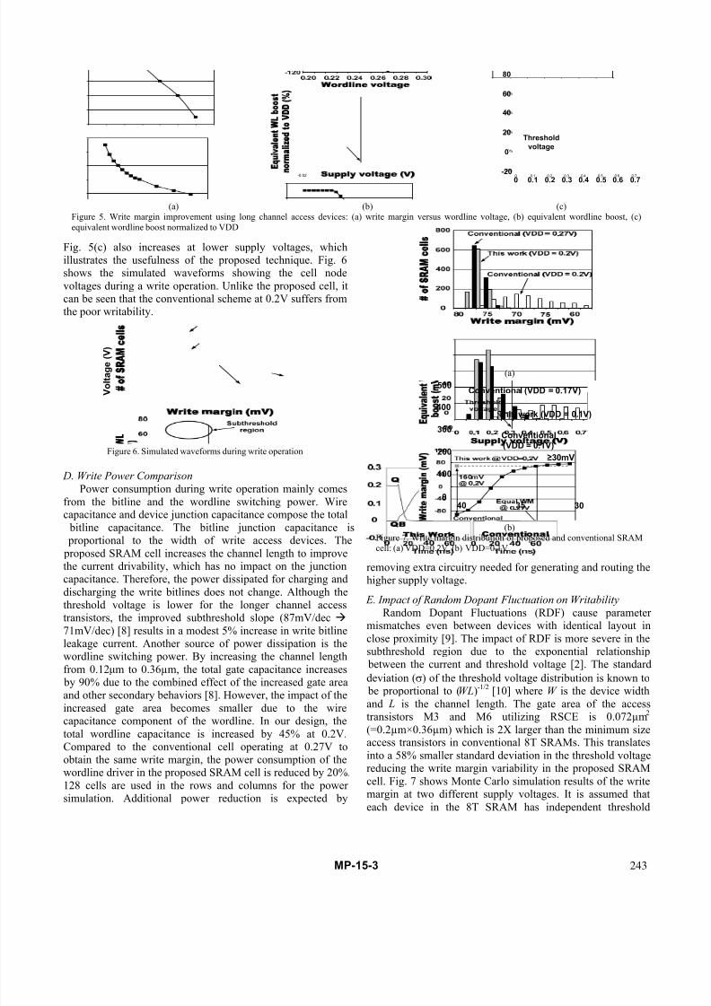
(b)Figure 7. Write margin distribution of proposed and conventional SRAMcell: (a) VDD=0.2V, (b) VDD=0.1V
Fig. 5(c) also increases at lower supply voltages, whichillustrates the usefulness of the proposed technique. Fig. 6shows the simulated waveforms showing the cell node
voltages during a write operation. Unlike the proposed cell, itcan be seen that the conventional scheme at 0.2V suffers fromthe poor writability.
V o l t a g e ( V
)
Figure 6. Simulated waveforms during write operation
D. Write Power Comparison
Power consumption during write operation mainly comes
from the bitline and the wordline switching power. Wirecapacitance and device junction capacitance compose the total
bitline capacitance. The bitline junction capacitance is proportional to the width of write access devices. The
proposed SRAM cell increases the channel length to improvethe current drivability, which has no impact on the junctioncapacitance. Therefore, the power dissipated for charging and
discharging the write bitlines does not change. Although thethreshold voltage is lower for the longer channel accesstransistors, the improved subthreshold slope (87mV/dec
71mV/dec) [8] results in a modest 5% increase in write bitlineleakage current. Another source of power dissipation is thewordline switching power. By increasing the channel length
from 0.12µm to 0.36µm, the total gate capacitance increases by 90% due to the combined effect of the increased gate areaand other secondary behaviors [8]. However, the impact of the
increased gate area becomes smaller due to the wirecapacitance component of the wordline. In our design, the
total wordline capacitance is increased by 45% at 0.2V.Compared to the conventional cell operating at 0.27V toobtain the same write margin, the power consumption of thewordline driver in the proposed SRAM cell is reduced by 20%.
128 cells are used in the rows and columns for the power simulation. Additional power reduction is expected by
removing extra circuitry needed for generating and routing thehigher supply voltage.
E. Impact of Random Dopant Fluctuation on Writability
Random Dopant Fluctuations (RDF) cause parameter mismatches even between devices with identical layout in
close proximity [9]. The impact of RDF is more severe in thesubthreshold region due to the exponential relationship between the current and threshold voltage [2]. The standard
deviation (σ) of the threshold voltage distribution is known to be proportional to (WL)-1/2 [10] where W is the device width
and L is the channel length. The gate area of the accesstransistors M3 and M6 utilizing RSCE is 0.072µm2
(=0.2µm×0.36µm) which is 2X larger than the minimum sizeaccess transistors in conventional 8T SRAMs. This translates
into a 58% smaller standard deviation in the threshold voltagereducing the write margin variability in the proposed SRAM
cell. Fig. 7 shows Monte Carlo simulation results of the writemargin at two different supply voltages. It is assumed that
each device in the 8T SRAM has independent threshold
243MP-15-3

8/8/2019 An 8T Sub Threshold SRAM Cell Utilizing Reverse Short Channel
http://slidepdf.com/reader/full/an-8t-sub-threshold-sram-cell-utilizing-reverse-short-channel 4/4
voltages which follow a normal distribution. Results areshown for a conventional SRAM cell at a nominal and a
70mV higher supply voltage. The average and the standarddeviation of of the proposed cell’s write margin are 79mV and
1.4mV, respectively, which are much better than those of theconventional cell (65mV and 15mV) at 0.2V.
Figure 8. SRAM read port Ion-to-Ioff ratio comparison
0.00
0.05
0.10
0.15
0.20
0.25
Figure 9. Bitline discharging speed comparison
(a) This work (b) Conventional
Figure 10. Proposed and conventional 8T SRAM cell layout comparison
F. Read Bitline Sensitivity Improvement
2X longer channel length devices are also used in theSRAM read port to increase the current drivability. M7 and
M8 in Fig. 3 have a channel length of 0.24µm, whichimproves read current from 11.6µA to 28.2nA. Further increase in channel length will further improve the current
drivability but this comes at an added cell area penalty. Owing
to the steeper subthreshold swing in longer channel devices,
the Ion-to-Ioff ratio improves from 169 to 271 as shown in Fig.8. The increased current drivability reduces the read bitline
discharge time improving the read performance. Fig. 9 shows
the bitline discharging speed comparison for the proposed and
conventional SRAM. Two different column data patternsgenerating maximum and minimum bitline leakage currents
are tested on a 32 cell column slice. The read delay is
improved from 88.9ns to 42.5ns and shows less variation for
the different column data patterns.
G. SRAM Cell Layout Fig. 10 shows the layout of the proposed and conventional
8T SRAM cells in a 0.13µm CMOS process. The write access
transistors and the read path devices in the proposed cell have
longer channel lengths. SRAM cell area was 4.42µm ×
1.44µm which is 20% larger than the conventional 8T SRAM
cell with minimum length and minimum width devices.
IV. CONCLUSIONS
We propose an 8T subthreshold SRAM cell with improved
write margin, better variation tolerance and increased Ion-to-
Ioff ratio in the read port. Process scaling makes RSCE
stronger due to the increased HALO doping used to negate theshort channel effect. In the subthreshold region, RSCE has an
even stronger impact on device behavior because of the
reduced DIBL and the exponential relationship between the
threshold voltage and weak-inversion current. Due to thiseffect, minimum channel length is not the optimal point for
maximum performance in the subthreshold region. To enhance
the SRAM cell writability, we use a 3X longer channel length(0.36µm) in the write access transistors to strengthen the
current drivability. The proposed SRAM cell at 0.2V achieves
nearly the same write margin as a conventional SRAM cell
with a 70mV higher wordline voltage. No additional supplyvoltages or circuitry are needed. Utilizing RSCE in the read
port increases the Ion-to-Ioff ratio from 169 to 271 and offers
a 52% speedup in read bitline discharge time. The SRAM cell
area overhead was 20%.
REFERENCES
[1] A. Bryant, J. Brown, P. Cottrell, et al., “Low-power CMOS atVdd=4kT/q”, Device Research Conference, pp. 22-23, 2001.
[2] B. Zhai, S. Hanson, D. Blaauw, D. Sylvester, “Analysis and mitigation
of variability in subthreshold design”, International Symposium on Low
Power Electronics and Design, pp. 20-25, Aug. 2005.
[3] J. Kim, K. Kim, C.T. Chuang, “Back-gate controlled READ SRAM
with improved stability”, SOI Conference, pp. 211-212, Oct. 2005.
[4] B.H. Calhoun, A. Chandrakasan, “A 256k subthrehsold SRAM using
65nm CMOS”, International Solid-State Circuits Conference, pp. 628-
629, Feb. 2006.
[5] C.Y. Lu, J.M. Song, “Reverse short-channel effects on threshold voltage
in submicrometer salicide devices”, IEEE Electron Device Letters,
Volume 10, pp. 446-448, Oct. 1989
[6] C. Subramanian, J. Hayden, W. Taylor, et al., “Reverse short channel
effect and channel length dependence of boron penetration in
PMOSFETs”, International Electron Devices Meeting, pp. 423-426, Dec.
1995.
[7] M. Tohmason, J. Prasad, J. De Greve, “Suppression of the reverse shortchannel effect in sub-micron CMOS devices”, International
Semiconductor Device Research Symposium, pp. 420-421, Dec. 2003.
[8] T. Kim, H. Eom, J. Keane, C. Kim, “Utilizing Reverse Short Channel
Effect for Optimal Subthreshold Circuit Design”, International
Symposium on Low Power Electronics and Design, pp. 127-130, Oct.
2006.
[9] R. Keyes, “The effect of randomness in the distribution of impurity
atoms on FET threshold”, Applied Physics A: Material Science Process.,
vol. 8, pp. 251–259, 1975.
[10] Y. Taur, T. Ning, Fundamental of Modern VLSI Devices, Cambridge
University Press, 2002.
244MP-15-4
Recommended

![Design and analysis of SRAM cell for ULP application... Timing Diagram of 8T SRAM cell 1.2.69T SRAM cell Figure.9. is the architecture of 9T SRAM cell[8]. It consists of 03 extra transistors](https://img.pdfslide.net/doc/110x75/5ace04837f8b9ad13e8ecb0a/design-and-analysis-of-sram-cell-for-ulp-application-timing-diagram-of-8t-sram.jpg)