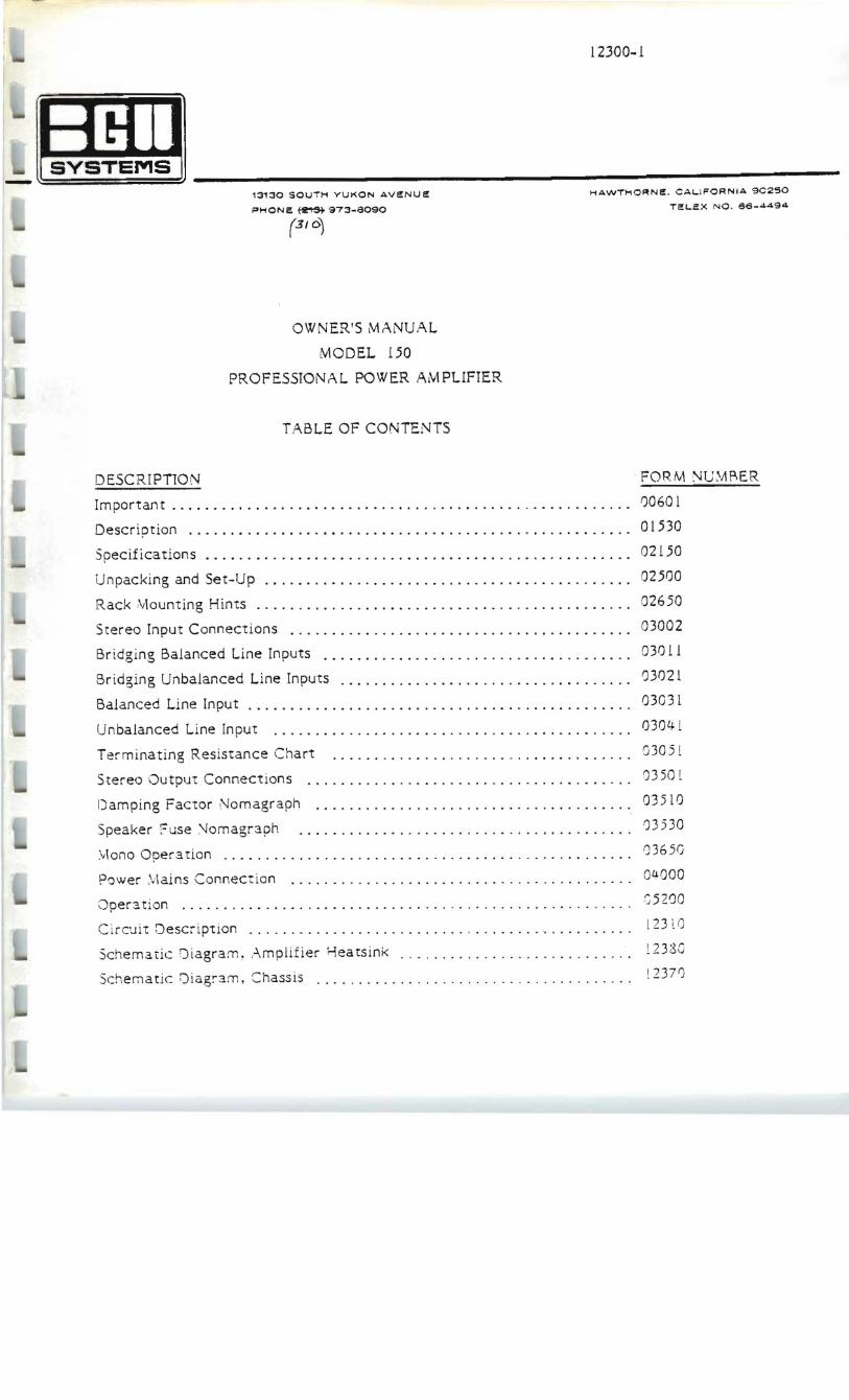
12300-1
1 SYSTEMS
13130 SOUTH YUKON AVeNUe HAWTHO~Ne CAllFORNIA 9C250
PHONe ~ 973-8090 TclEX NO 66_4494
(310)
OWNERS MANUAL
MODEL 150
PROFESSIONAL POWER AMPLIFIER
TABLE OF CONTENTS
FORM NU~APERDESCRIPTION
Important 1)0601
DescriDtion 01530
Specifications 02150
Unpacking and Set-Up 02500
Rack Mounting Hints 02650
Stereo Input Connections 03002
Bridging Balanced Line Inputs 03011
Bridging Unbalanced Line Inputs 03021
Balanced Line Input 03031
Unbalanced Line Input 03041
Terminating Resistance Chart 03051
Stereo Output Connections 0350 l
Damping Factor Nomagraph 03510
Speaker Fuseiomagraph 03530
vlono Opera tion 03650
Power Iains Connection ouOOO
Opera tion 05200
Circuit Desc-iption 123li)
Schematic Qiagram~ -mplifier f-leatsink 12 380
Schematic Qiagam Chassis [2371)
12300-2
Schematic Diagram AC wiring 12360
Block Diagram Power Amplifier 12350
Parts List 12390
00601
-IMPORTANTshy
PLEASE READ THIS PAGE BEFORE OPERATING
YOUR
BGW POWER AMPLIFtER
Your new BGW amplifier is designed to provide years of trouble free performance
Observing these few precautions will insure proper operation
All connections should be made to the power amplifier with the power OFF
Speaker fuses should be used to afford maximum speaker protection
Never connect the output of one channel to that of another
Connect the power cord to the proper voltage mains as indicated on the rear of the amplifier ConverSion to another voltage requires internal rewiring
Do not remove the amplifiers cover Amplifiers may not be covered under warranty if they are tampered with There are NO adjustments within Potentially lethal voltages exist within the amplifier Refer all service work to an authorized BGW service station
01530-1
DESCRIPTION
The BGW Model 150 is one of the most advanced solid state fully complementary bridgeable stereo power amplifiers available
Features of the Model 150 include precision step attenuator leve1 controls LED metering separate circuit and chassis grounds XLR and Y4 input connectors with transformer sockets and small size
The front panel includes two vertical rows of four red LEDs one row for each channel The lower LED in each row is the IDLE indicator or pilot lamp They will be lit whenever the amplifier is turned on
The top LED in each row is a clipping indicator and utilizes an exdusive BGW circuit Whenever either channel of the 150 is driven into clipping a corresponding indicator lights and remains lit for 020 seconds These indicators which actually indicate loss of feedback tell the operator that the amplifier is being overdriven and can be invaluable to the engineer who must be sure that every component in his system is producing a clean distortion-free signal An inadvertant short-circuited output (with signal) will cause the LED to remain on until the short is removed
The midd1e LEDs are connected to a circuit employing integrated circuit to provide an audio level indication of 05 and 50 of maximum power output They provide a valuable tool for total system evaluation in multiple amplifier installa tions
Both the circuit and chassis grounds are connected to separate barrier strip term inals on the rear of the amplifier They are connected together by a removeable link By removing the link the circuit grounds of all active units (amplifiers preamplifiers mixers etc) can be tied to earth ground at a common point This aids in eliminating ground 100ps
Ei ther XLR-type of V4 inch phone plugs may be used for input connections If plugshyin transformers are used the XLR-type connectors are connected If not jumpers must be employed in the transformer sockets See sections 03011 03021 03031 and 03041 for details
The size of the todei 150 is convenient for a wide variety of applications However please note the following precaution
1) Do not use the front panel as the sole support for the am plifier Side rails or rack sheives should be employed (See section 02650)
The output stages of your amplifier use the most advanced type of transistors available These large geometric complementary power devices have large safe operating areas and extended power bandwidth Electrostatic and other highly reacti ve speaker systems present no difficulties for the odel 150 The aluminum heat sinks are located so the 150 power amplifiers can be stacked on top of each other and air can be forced through both sides to cool the products
01530-2
AU of the semiconductors in the output area are in intimate contact with the heat sink The bias circuit is also mounted on this isotherm to provide rock steady bias stability with temperature
The voltage gain circuits are also mounted on the same circuit board A true operational amplifier integrated circuit acts as the front end
The op-amp is a special unit featuring very low noise high speed (lOMHz) The opshyamp stage is followed by a discrete complementary pair acting as an active current sourcesink and providing voltage gain The current source is the ideal way to drive the output stage which is basically a triple Darlington voltage follower
This sophisticated circuit design makes for an extremely accurate amplifier The accuracy of an amplifier is a function of the ratio of the open loop gain to the closed loop gain In this case the open loop gain is about 1000000 This extremely accurate signal processing enables the amplifier to drive speakers at very high levels while adding absolutely no coloration of its own Even at milliwatt levels the output waveform exhibits no sign of crossover distortion
02150-1
THE BGW 150
PROFESSIONAL POWER AMPLIFIER
Exacting design standards and unique features establish the BGW ampJifier as the industry leader in power amplifier technology Features such as all steel chassis and covers metal-case output uansistors and totally modular construction have set the industry standard in audio power amplifiers
Delivering a full 50 watts per channel into 8 ohm loads and using the latest in full complementary circuitry techniques the Model 150 offers reliability and performance unparalleled in the industry
SPECIFICATIONS BGW MODEL 150
OUTPUT POWER
50 watts minimum sine wave continuous average power output per channel with both channels driving 8 ohm loads over a power band from 20Hz to 20kHz The maximum Total Harmonic Distortion at any power level from 250-milliwatts to 50 watts shall be no more than 05
75 watts minimum sine wave continuous average power output per channel with both channels driving 4 ohm loads over a power band from 20Hz to 20kHz The maximum Total Harmonic Distortion at any level from 250-milliwatts to 75 watts shall be no more than 08
150 watts minimum sine wave continuous average power output monaural driving an 8 ohm load over a power band from 20Hz to 20kHz The maximum Tota l Harmonic Distortion at any power level from 250 milliwatts to 150 watts shall be no more than 08
All specifications and features are subject to change without notice
Intermodulation Distortion
Small Signal Frequency Response
Hum and Noise Level
Input Sensitivity
Input Impedance
Damping Factor
Output Impedance
Power Requirements
Semiconductor Complement
Dimensions
Weight
02150-2
SPECIFICA TIONS
Less than 00296 from 250 milliwatts to rated power
+0 3dB 1Hz to 100kHz +0 025dB 20Hz to 20kHz
Better than 102dB below 50 watts (unweighted 20Hz to 20kHz)
10 volts for maximum power output Voltage gain 26dB (20 times)
15K ohms
Greater than 400 to 1 Referenced at 8 ohms at 1 kHz
Designed for any load impedance equal to or greater than 4 ohms
100 120 200 220 or 240 volts 50-60Hz 350 watts
2 Ultra-low noise Op Amp ICs 2 level detector Ies 2 delay timer ICs 26 transistors 4 zener diodes 12 diodes 8 LEDs
1 34 by 19 standard rack front panel Depth behind front panel 11Y2 (445cm X 4826cm X 2921cm)
14 lbs (637 kg) net l8 Ibs (818 kg) shipping
02500
UNPACKING AtfD SET-UP
Your 8GW Power Amplifier is shipped in an advanced packing container
SAVE THE CONTAINER AND ALL PACKING MATERIAL
The container should be saved in the event the unit is moved or shipped at some future date Replacement containers are available from BGW Systems for $1400 freight included
Inspect the unit for damage in transit immediately upon reshyceipt If damage is found notify the transportation company immediately Only the consignee may institute a claim with the carrier for shipping damage 8GW will cooperate fully ~n such event Be sure to save the container as evidence of damage for the shipper to inspect
The amplifiers mounting position must be chosen carefully so that the air flow to the sides of the unit is not restricted Inadequate ventilation may cause the protectie heat sensors to shut the ~nit off For rack mounting the four rubber feet on the bottom of the unit may be removed and no hardware will be loosened inside the unit
DO NOT PLUG THE AMPLIFIZR IN YET
All connections should be made before power is applied
02650
RACK MOUNTING HINTS
KEEPING IT COOL
A power amplifier draws energy from a primary electrical service usually a 120 VAC outlet to drive loudspeaker systems with an audio signal Typically only half of the energy can be delivered to the loudspeakers remaining energy is converted into heat and must be dissipated (ventilated) into the air
Air circulating past heat-producing components absorbs the heat and carries it away To accomplish this low and medium power amplifiers rely on natural convection currents while most high power amplifiers use fans If the air flow is impeded the resulting rise in heat may cause an amplifier to stop working or fail
Circulating air currents must not be cut off when installing power amplifiers in racks Power amplifiers using convection cooling require spacing between amplifiers to permit air flow between them Power amplifiers using forced-air cooling on the other hand can usually be stacked closer to each other and may not need any blank panel spacing between amplifiers
To improve natural convection currents within a rack a chimney can be created by closing the back of the rack and venting the rack at the bottom to let in fresh air and at the top to exhaust hot air Vents should be large rectangular slots approximately 19 wide by 4 high
The rack cabinet will require some type of blower if a large air-flow is required It is best to exhaust air from the top of the rack rather than to blow it in from the bottom There will be less dust and dirt in the rack this way if the bottom vent is sufficiently large
INSTALLING THE UNITS
Use care when mounting equipment in a rack Place the heaviest units near the bottom of the rack and fill in all unused rack spaces with blank panels Equipment cannot always be supported by front panels alone This is especially true of amplifiers whose depth is more than twice their height Uniform support can be insured by instaUing bottom or side rails
When racks are to be transported or used in a mobile installation some means of securing the rear of the equipment are required Angle brackets either attached to the bottom side rails or rear panel are practical approaches
03002-1
STEREO INPUT CONNECTIONS
Three-pin XLR and 1 in phone jacks are provided on the rear of the amplifier for inpult connections Balanced or unbalanced lines may be used however if input cables are longer than 8 feet balanced lines may be necessary to maintain the signal-to-noise ratio and high frequency response
14- INCH PHONE JACKS The 114 phone jacks are for unbalanced lines only (single conductor shielded) and may be used directly Simply connect the shield to the outer sleeve of the plug and the inner conductor to the tip or buy ready-made cables See diagram below
CONNECT SHIELD HER~-
JJ - r ~ t 10 CONNECT INNECONDUCTOR HERE SLEEVE TIP 3-PIN XLR CONNECTORS The 3-pin XLR connectors may be used with balanced (2-conductor shielded) or unbalanced lines They are connected to the amplifiers inputs by using the 8-pin transformer socket they cannot be used directly
Unbalanced Lines To use the 3-pin XLR connectors with unbalanced lines a jumper plug (BGW PiN 1350-0 1 08) must be inserted into each transformer socket The jumper plug connects pin III to pin 117 and pin 116 to pin 118 as shown
With the jumper plug in place the 3-pin XLR connector has pin JUMPER PLUG 2 connected to
MUST BE USED ground and pin 113 toWITH the input of theUNBALANCED amplifier Note RearLINES of plug shown
When using single conductor shielded cable for unbalanced lines connect the inner conductor to pin 13 and the shield to pins 111amp 112
J--~ When using 2-conductor shielded cable for unbalanced lines connect the high level signal wire to pin 113 the low level signal wire to pin 112 and the shield to pin Ill
Note Shield not connected to anything at signal source
03002-2
To achieve a true balanced input it is necessary to use one transformer for each input These should be plugged into the octal sockets provided Depending on the specific application one of several different transformers may be selected
Forms are included in this manual to help guide you in your use and selection of transformers Use the index below to find the appropriate form to match your needs
CONNECTING ON SOURCE TO ONE AMPLIFIER
Using Balanced Lines Refer to form 1103031
Using Unbalanced Lines Refer to form 110304-1
CONNECTING ONE SOURCE TO TWO OR MORE AMPLIFIERS OR DEVICES
Using Balanced Lines Refer to form 1103011
Using Unbalanced Lines Refer to form 1103021
NOTE Each amplifier input will be referred to as the Load in the above mentioned forms Only one channel will be shown
Two conductor shielded cable should be used in a balanced line system Connect input cables as shown below
Pin If 1 Shield (Ground) Pin 2 Signal (Minus) Pin 113 Signal (Plus) -~ I-L=-~-3
FOR MONO (BRIDGED) OPERATION
To operate the unit as a mono amplifier use the left channel input only DO NOT use the right channel input Remember to place the stereomono switch in the mono position
I
r(
load 112
03011
BRIDGING BALANCED LINE INPUTS
Used only when two or more devices are driven from the same input line
r- 3
I
600 ohm 2
W 1 I
SOURCE 1 r---rlt D ~ I--)~ 1000shy
load I load III liN
MAXIMUM NUMBER OF AMPLIFIER 25ea
Input transformers for above
A Use 1 1 transformer 600 ohms to 600 ohms
B Nth load must have a terminating resistor added to the secondary of the Input transformer
rOne alternative configuration is
C l 1 transformer 15K ohms to 15K ohms
D Nth load must have a terminating resistor added to the primary of the input transformer
To find this resistance value see sheet TERMINATING RESISTANCE CHART MFRM 03051
NOTE Terminating resistance is required when source is a transformer Sources other than a transformer may not need a termination
03021
BRIDGING UNBALANCED LINE INPUTS
Used only when two or more devices are driven from the same Input line
600 ohm HI ~~------~------------~--------~
SOURCE LO
load 111
load 112
load liN
The Nth load should have a terminating resistor added to its octal plug between pin 1 and pin 6
To find this resistor value see sheet TERMINATING RESISTANCE CHART MFRM 03051
NOTE Terminating resistance is required when source is a transformer Sources other than a transformer may not need a termination
03031
BALANCED LINE INPUT
Used only when one amp~ifler is driven from one source
600 ohm _ - - ( ) LOAD
Source -I
Input transformer for above
A Use 15 transformer 600 ohms to 15K ohms
NOTE No 600 ohm TERMINA nON IS REQUIRED
B Alternate transformer
Use 1 transformer 600 ohms to 600 ohms
NOTE 600 ohms termination is required on the secondary of the transformer
NOTE Terminating resistance is required when source is a transformer sources other than a transformer may not need a termination
600 ohm termination when required can be accomplished by soldering the resistor across pins 1 and 6 of the transformer as shown below
600 6HMS
or by installing the resistor in a 14 phone plug and inserting it into the unused unbalanced input jack
03041
UNBALANCED LINE INPUT
Used only when one amplifier is driven from one source
600 ohm 1
LOAD I
- - Source
A 600 ohm terminating resistor-- must be added to its octa plug
Between pin 1 and pin 6
NOTE Terminating resistance is required when source is a transformer Sources other than a transformer may not need a termination
600 ohms
03051 middot
TERMINATING RESISTANCE CHART
How to find terminating resistance for balanced or unbalanced 600 ohm lines driving more than one amplifier
STEP A Input Impedance of Amplifiers = Total Load ImpedanceNumber of Amplifiers of Amplifiers
STEP B Total Impedance of Amplifiers - 600 K (Impedance=Factor)
600
STEP C ( t+~ x 600 ohms = Load Resistor Required
EXAMPLE Input Impedance of Amplifiers = 15000 ohms Number of Amplifiers = 4
A 1~000 = 3750 ohms
B 3750-600600 = 525
1C 525 +1 x 600 = 119 x 600 = 71429 ohms
Closest value is 715 ohms 1 metal film resistor
Note all amplifiers must have the same input impedance If not use formula below
i = Total Load Impedance
EXAMPLE Four (4) Amplifiers with input impedance of 15k
30k 30k and 75k
1 = 3750 ohms
I -t IS( + 30~ + 30K -7SK
0301-1
STEREO 0UTPUT CONNECTIONS
Two sets of five-way binding posts on the rear pane serve as output connectors with one black and one red binding post fOl eadl channel Left channel leads go to the blnding posts marked LEFT right channel to those marked RIGHT
Output leads are best connected to the amplifier with standard banana plugs however the five-way action of the binding posts permits the use of tinned wires or spade lugs
Make certain that the speakers are properly phased Connect the black or minus (-) terminal on the speaker cabinet to the appropriate black binding post on the amplifier Connect the red or plus (+) terminal to the red binding post Check to see that the stereQ-mono switch on the rear of the amplifier is in the stereo position
SPEAKER PROTECTION
All speakers can be damaged by having too much power applied to them Fuse protection is an effective- and inexpensive way of preventing this from occurring Ii your speaker system- does not contain a fuse or a circuit breaker a fuse should be placed in series with each speaker and the wire going -~o the red terminal on the rear of -the amplifier bull - shy
Maximum protection can be obtained with fast-acting fuses - Use the value recommended by the manufacturer Ii no value is specified use the chart provided to select the correct value (MFRM-03530)
To use the chart take a straightedge such as a ruler and line up the speakers impedance with its peak music power rating The proper fuse value can then be read from the center column Choose a fuse that is closest to and below the value indicated
WIRE SIZE AND DAMPING FACTOR
The high damping factor ot BG W ampiiiiers results in a very dean bass response Excessively long and small diameter speaker wires can lower the damping factor and distort the lower frequencies A damping factor of at least 50 should be maintained to insure good audio quail ty
The relationship between wire length and diameter and damping factor can be calculated using the chart (MFRM-03510) on the following page Proceed as follows
1 Using a straight-edge line up the gauge of the speaker wire with its length Mark ofi the resulting source resistance where this line crosses the center column
2 Line up the source resistance determined in step III with the manuiacturers impedance ot the speaker system The damping factor can now be read
03501-2
+The impe-1ance of a speaker sys-rem can be approximated by measuring the resistance across the speaker terminals wit1 the amplifier disconnected Multiplying this result by 133 gives you the approximate impedance
Note This method cannot be used with electrostatic speaken
bullbull
-l Is AHNIAUD LOAO SOUacl COltPO
lI51STAHCI ISISlANeI WIbullbull t_1 t_eI taneeeftl tAwet
shy1-IS
OAMfltNG lO
ACTOil
ISO 21_ JOO
2-lt CAaU
SO
IS 20
SOURCE RESISTA1lCE AND DAMPING FACTOR VS LENGTH AND SIZE OF OUTPUT LEADS
MFRM - 03510
-28
20
1
5
bull
12
1 l
16 A
~ 20
2 25
J5
30
00
300
200
150
lao ao
60
0 30
1 20
15 PEAK I
10
bull MUSIC
POWER (watts
6
4
3
2
15
SPEAKER l FUSE SPEAKER () (
EXAMPLE ~z 8n PEAl( POWER = 15 OW Al~SWER FUSE = 2 NIPS
FUSE SELECTOR NOHOGRAPH FOR LOUDSPEAKER PROTECTION
MFRM -03530
03650
MONO OPERATION
The output power of the amplifier can be increased by operating it in the mono (bridged) mode The correct procedure for mono operation is as foHows
1 Set Stereomono switch to mono position
2 Use lett channel input only DO NOT use the right channel input
3 Connect the output across the two red binding posts DO NOT use the black binding posts DO NOT reference the load (speaker) to ground Designate the left channel red binding post (+) and the right channel red binding post minus (-) Fuses when necessary should be placed in series with one red binding post
RIGHT LEFT
STEREO RIGHT LEFT
I ~UT-Iiei I II I
I = I ~N~L~J MONO MAKE OUTPUT CONNECTION
TO RED BINDING POSTS SET SWITCH TO AONO POSITION
MAKE INPUT CONNECTION TO LEFT CHANNEL INPUT
NOTE Minimum load impedance for mono operation should be 8 ohms
CIRCUIT DESCRIPTION
In the mono mode the output at the left channel is fed into the inverting input of the right channel The two channeis work opposite each other when one goes positive the other goes negative thus doubUng the output voltage swing The single output is referenced between the two red binding pOSLs
04000
POWER MAINS CONNECTIONS
The unit should be plugged in only when it has been established that it is wired for the correct power mains voltage and after all other connections have been made
The mains (AC line) voltage is indicated on the label on the rear of the unit Products supplied for use in the United States and Canada are factory wired for 120 volts Only the indicated mains voltage should be used If the mains voltage must be changed see POWER MAINS VOLTAGE CONVERSION
A molded parallel blade U-ground plug is supplied This connector is standard in the United States and Canada For use elsewhere the plug must be replaced with the correct connector The color-code of the cord is as follows
HI (switched Leg) - Brown (or Black) LO (neutral Leg) - Blue (or White) EiR TH (chassis ground) - Green with Yellow tracer (or Green)
OPERATION
PRECAUTIONS
1 Speaker destruction is often due to improper equipment operation This often occurs when someone without the proper appreciation for the components of a high power high quality music system has the opportunity to change records or adjust levels The best protection here is caution Keep the equipment out of reach of untrained adults and children Make sure the speaker is properly protected with fuses (Output Connections Section)
2 Never parallel the two amplifier outputs together
3 When driving any load with an impedance of less than 4 ohms the load should be isolated from the amplifier with a series capacitor in order to avoid both damage to the load and wasting of output power
4 If the amplifier continuously blows fuses something is wrong - do not increase fuse size
5 Do not connect an input ground lead to an output ground lead to do so may cause a ground loop and oscillations
6 Do not operate the amplifier from power mains which exceed the indicated mains voltage by more than lO
7 Never connect the output of the am plifier to another power source such as a ba ttery or power main
8 Do not expose the amplifier to corrosive chemicals such as lye soft drinks salt water etc Also never immerse the amplifier in any liquid
9 Do not remove the amplifiers cover during operations
10 The amplifier is not intended for high frequency-high power use and should not be used for high power at above 20 kHz
11 Neither the amplifier nor any of its leads should be exposed to areas likely to be struck by lightning
PROCEDURES
After all connections have been made to the power amplifier turn the gain controls fully counter-clockwise Turn on the preamplifier then turn on the power amplifier The LED over the circuit breaker or marked IDLE should light If it does not check to see that the amplifier is plugged in to a live power outlet
05200-2
With the preamplifer gain controls fully off advance the left and right power amplifier gain controls about half way clock-wise (slit in knob facing upwards) There ahould be no audible hum if a hum is heard check the connections between the power amplifier and preamplifier Now advance the preamplifier gain controls untiJ the desired maximum volume is achieved Should the preamplifier gain control be in excess of the 34 setting decrease it to half volume and increase the gain controls of the power amplifier to the desired level
Often turn-on transients originate in the pre-amp or tuner This is especially true of tube-type units If this situation arises turn the amplifier on after the other units have had adequate time to stabilize
12310
150 CIRCUIT DESCRIPTION
Both channels of the amplifier operate in the same manner and only the left channel will be explained
POWER SUPPLY
The AC input power from P501 passes through the Circuit breaker CB 301 From CB 301 the AC goes to the power transformer T301
The output of T301 goes to a full wave bridge rectifier capacitor input filter circuit consisting of 0301 C302 and C303 to give a positive and negative power supply voltages
AMPLIFIER
The input signal from J 301 is applied to the R301 input level control The output from R301 is applied to the inverting input (pin 2) of op amp IC 103 through the coupling network CI0l RI01 CI02 and RI04 This network provides a high impedance to the amplifier and filters out DC and radio frequency interference
QI03 and QI04 divide the signal into positive and negative components respectively They are connected common emitter and provide voltage gain QII0 and Ql1l are connected common collector to provide the current gain necessary to drive the output stages Q 112 and Q 113 The output appears across fly back clipping diodes 0103 and 0104 then passes through compensation networks LlOlR128 and R130C1l7 and thermo switch 5101 to appear at output jacks J308 Switch 5101 opens if the output transistors reach 100 degrees C
To maintain overall stability linearity and low distortion degenerative feedback is used throughout the amplifier Voltage divider R 103C 106 and R 106 applies the correct amount of feedback to the non-inverting input (pin 3) of op amp IC 103 Except for the input the amplifier uses direct coupling throughout Q 106 and Q 107 provide the current limiting necessary to protect the output stage
BRIDGED MODE
When the monostereo switch 5301 is set to mono it converts the right channel amplifier to a unity gain inverting power amplifier
5301 tvlonoStereo switch grounds the normal input to the right channel and connects the output of the left channel amplifier to drive the right channel sum ming point RIO 2
I I t
~ -1
1-
w bull10 bull
I
v-a
_L
it-
Il1 -I~
1 )~-
0 ~ ~
~ ru
I~t
t~C14middot bull 11amp rc bull ~ bullbull___-+-_
CO
~1~t
-Jfl~L I~ lP-f~
1-
~Lmiddotf ~ I ~
cJPI
100
1-lt
4gt1
~II ~( a
i ~)
11 Q
r~
1 ~-O- I
IOn
I t I
~I
J16 I
~
01 fI~Or
I
I I I
I I
I
t
i I
NOTES Ut-ll ESSOIII(IIWISE SPfClnEO
bull t~I~J~(middotmiddotmiddotmiddotmiddot
QS IY r~ so I t
gt 1 0I 1
- _I
IIHlln OtllRWlU srorolD BGWSYSIEMS 13130 SOUlIlYlJKOIIIIIIIE
O_HSIOttttQ NtD 0l(AAHCampHQ tIAWlllOIINECA 9O50 n - 1IJI9738090POI~ YIIS W
HllONl bullbull III nltCIIU IIIWII 5D 6~~Tlt IIpoundr~~t PLY AnLR rUII1IlPRELIMINARY alleo(IlIUIlAHCI Ole 5 JD( bull oJ J()IX bullbull1 fOl(aJrf1Ct ON AIGUS _ bullbullbullbullDOCUMENT bull UK SlIM (nGll lUO totAl
flEVsoatAtl IIIlIJOIOHl 55 Ie-
FOA REFERENCE ONLY
DO NOr Ir ORAwllOCl
-----
------
R[VISIONS u ppAOVlOOlsatrlOC 0(
Clffol - shy -i bull - Gmiddotmiddot
fL
- shy~-J ~ 91ut ~~-=
I amp I
~ __ t
oo~ p-- ~t(L)
Pry J- ~~
tLLi ~
cpound
)
11113~ IJHIUS OlllERWlst S(ctmD
11~3 1- 01[5000 0 lOl[AAlOC1tO (0 (lSAS YIU
ptUpoundHUlHS AIII( IN tCH(s
(= [~c7~
I XI( == OJ DJ( - 2 010 lOlflllAHC( Oft AtlGlU J Omiddot bull
81(M SIAP (ocrs YoU
SIIfAC[ ft()UG~US Ie- 1
NOT E S UNLESS 011 EIWISE SPEClf lEO----i DO ~o Sr
bull ~~t~-middot~~ n-r
1 rL VIgt bull~1 (D
~ ~ I
~~~_llULL I Ilttl
~ __ I lOOe p-n ~f(pound)
1
--IL J P~lt
Iii I Ii
tl-ol G-
T 0 -lb1gt
~ +Icc
50)
IJ 7~ -t~
shyPRELIMINARY DOCUIVIENT
FOR REFERENCE ONLYW BGWSYSIEMS
-1_ -~LLV
~I~ i I OO - II t1S I
llt-flOgt
IlJt~8iigp~~t~~~Evr 12131913 B090
(IfIAWlt IU
tv IIJ CIsssCiilCK--- --- 5b
DltAWO 00( A nEV J37D
~ l( ORAWIlIO
I
t-c~
6U (IV )
-ZOV
~
0 6dI ltgt~t- 6coJ
7
Cgtv(w-)
I()O V
~1UJifJ
6ur
Bv(lJ-
-ztfOV
NOTES ur ES501~nWISE SPEClflm 00 riOT SCN [ ~V1Ha
R[VISIONS
Ull O(SCIIIKlH DAl( AlPnOV(O
) baJ-~~ 0 sect~) ~
rh ~ 3 ~
-zoov
-=9 )ti6L1 - -~-----0 -shy - cshy
rt7
PRELIMINARY DOCUMENT
FOR REFERENCE ONLY
220V
UHll$S 01 H(RWIS[ snCIUfO
OIM(HSIONltfC AND 100VlNfCIHO r tSA$1 YIU
UMOtSIOH5 Nt( Iii IIfCti(S AtIO APPlt ATTU PlArtHO
rouflulaquol Off ()(CU-I Ja Ell t J)J JIXIl = 010
JOl(llHC( ON AHGlU a lD
IUA Slwtr (1)((5 bull 10 MAJ
IUlfAC[ ROtKOtipoundS5 Ie
tRofCI (Hajj
Ll
SIll
c SCA(
tUJ~ ISb
L-__ shy-r
~--- cshy -shy(~
~
2-_
IlGW~Y5EMS 13130 OUllt YlJI(ON AVE tiW tOt INECA 9025f1 12131913middot8000
L0lfl ~( Fc Dot-Egt Ie (rpoundE 1610-
Ico ( 116~ S OAAWIIKI NUItAMIII
- -lt3t()
SltUl l
BGW SYST~~S INC
ENG NO DESCRI~TlaN PART NO
PARTS iIST 150 ~ 12390
SCHEMATIC AC wIRIN~ MFR~ 12360 SCHEMAT[C CHASSIS MFRM l2370 SCHEMATIC HEATS[NK MFRM 12380 B~OCK ~IAGRAM MFRM 12390
A~L COMPONENTS _ITH DESIGNATIONS IN THE 200 SERIES ARE RIGHT CHANNEL HEATSINK NUMBERS - ~EFER Ta 100 SERIES NUMBERS EXAMPL~ 201 ~aULD BE THE SAME AS CIOl
CAPACITORS
1gt1 47 UF 2SV TANTALUM CI02 240PF SUOII MICA CI03 10PF 10011 MICA CI04 30 PF 50ull1 CA CI05 47UF 10V E~ECTR~~YTIC CLOt) 30PF SOu II ~ICA
Clgt7 12UF 10011 META~IlE) ~YLAR
(lO~ 12UF 10011 META~IlEJ MYLAR CI0 220PF 500 DISC C 1 1 ) lUF 2511 JISC ell 1 lOOOPF 50011 DISC (112 1000PF 5001 DISC C113 S60PF 5uOll MICA C 1 14shy 240PF 50011 MICA Cl15 l2uF 10011 ~ETA~IlEJ ~YLAR Cl15 12uF 10011 METALILEJ MYLAR Cl17 12UF 100V METAiIlEJ MYLAR Cl1 1UF 25 )I5C Cll~ bull 1 UF 2511 J I SC C12) 1UF 2511 JISC 121 015UF 10011 MYLAR C122 1UF 25 JISC (123 47uF 10011 META~ILEJ ~YLA~ C 12+ 1UF 2511 )IiC C125 430PF 100 IICA C12l tUF 2511 DISC C301 OlvF 50011 DISC C302 8500UF SOli E~ECTRQLtTIC
C3gt3 8500UF 501 ELECTqQLtTIC C304shy 01UF 25 JISC C3JS OluF 25V JISC
0226-0005 0090-0240 0060-0010 0060-0030 0456-0047 0060-0030 0363-9003 0363-8003 0100-0220 0129-0100 0100-1000 0100-1000 0080-0560 0090-0240 0363-8003 0363-8003 0363-8003 0129-0100 0129-0100 0129-0100 0369-0015 0129-0100 0363-3000 0129-0100 0060-0430 0129-0100 Ot99-0100 0533-IJOOd 0533-0008 0129-0100 0129-0100
ENG NO
=gt101 0102 )103 01 +
~1S 0100 ) 107 ~10j
~3Jl
rcia 1 IC1J2 r C 103
J 1 J 1
J301 J302 J3JJ J 3J 4
J305 J30~
J307 J30~
J30~
J310 J311
1 0 1
P3J1 PJOZ
JIJ1 0102 0103 01J4 (HOS
01)6 0107
12390-2
BGw SYSTEMS lNC
OESCRIPT[J~
DIODES PART 0
IN41461N914 OI~DE IN414d1N914 DIODe IN400~ DIJDE lA 400V IN4004 DIJDE lA 4QOV lN4740A IOV ZENER DIODE IN4740A IOV ZEN~R DIODE 1N414d1N914 DIODE IN41481N914 DI~Dc B~IDGE RECTFIE~ ~Brl2502
1900-4148 1900-4146 1900-4004shy1900-4004 1900-4740 1900-4740 1900-414d 1900-4148 1886-2502
INTEGRATED CIRCU[TS
LEVEL DETECTOR TI~ER ~~555
OP AMP NE5534
TL0467CP 1685-0487 18d5-0555 1685-5534
JACKS
MOLEX 12 ~IN CO~NECTOR 03-09-2121 INPuT JAClt Nlll r NPU r J A Clt Nil 1
6 PIN SQCtltET 6 PIN SOCKET 3 PIN XLR PC ~O~NT 3 PIN XLR ~C MOUNT STE~EO PH~NE JACK 39 BUSHING CJNNECTQR 3INDI~G POST RED CONNECTOR 3INDr~G POST RED CJNN~crOR 3IN~I~G POST BLACK CONNEcrOR 3INDI~G POST BLACK
1231-2121 9999-0111 9999-0111 1203-0006 1203-0008 1205-0002 1205-0002 1205-0005 1231-0008 1231-0008 1231-000~
1231-0009
I ~DUCTOR S
14JH INDUCTOR 22GA MIRE 8022-0400 SEE R128 1700-0001
PLUGS
MOLEX MOL~X
12 12
~IN ~O~NECTOR 03-09-1126 ~IN CO~NECTOR 03-09-1126
1231- 1 1 26 1231-1126
TRANSISTORS
2N2484 NPN SI~ICON LOW SIGNAL r09~
MJE lSO~8 rRANSISTOR NPN r0220 MJE 350 PNP r~ANSlsrOR
MJE J~O NP~ T~A~SISTOR
MJE 720 N~N rRA~SISTOR
2N4401 NPN 5r~ICON LO~ SIGNAL r092 2N4403 PNP SI~ICON LO~ SIGNAL rU92
1654-2484 1854-5028 1953-1) 350 1954-0340 l854-0720 l654-440 1 1853-4 03
123903
8G- SYSTEMS INC
ENG N) 01 Js 010~
0110 ) 1 1 1 ell 12 0113
Q10l ~lJ2
~ 1 J 3
RI04shy
U 15
RlelS ~107
HD~
~lel~
~110
~ 1 1 1 ~ 11 2 R113 en 1 4shy
~ 115 lt1 1 ~ R 11 7 ~11i
R 1 1
R12J ~ 1 2 1
~122
en 23 ~124-
~125
~12)
~127
~12j
~121
~13()
R131 ~132
R133 R134 R135 R13S R137 R138 R13~
R14J R 1 ~ I
Rl~2
DESCR1TI31 4JE 340 N)N THAlS 1 STO~ MJE 350 PNP TRAt4SISTOR MJ E 15028 NPN T~ANSISTOR T0220 MJE 15029 PNP TRANSISTOR T0220 MJ 15022 NPN TRANSISTOR T03 MJ 15023 ~P T~1SISTOR T03
RESISTORS
47K 5X 12~ DEPQSITED CAR~ON 475K IX ~ETA~ FI~M 475K 1~ ~ETA~ FI~M
~7K 5~ 12~ DEPOSITE~ CARBON 47K 5X 12w DEPOSITED CARBON 24~K 1~ META~ FI~M
100~ 5 12~ DEPOSITE3 CARBON 15K 5 12WDEPuS1TED CARBON 15K 5~ 12~ DEPOSITED CAR~ON 0~0~ 5 12w DEPOSITE3 CARBON odOR 5 12M DE~OSITEJ CARBON o~R 5 12~ DEP~SITED CARBON 1JOR 5 12~ DEQO~ITE3 CARBON FACTORY SE~ECTEJ aFFSET ADJUSTMENT 27~ 5 1211 0E~OSITED CARBUN 470R 5 12~ DEOSITE) CARBON FACTORV SE~ECTE3 alAS ADJUST~ENT 100R 5 12~ DE~OSITEJ CARBON 100R 5~ 12~ DE~OSITEJ CARBON 1~ 5 12M DEPOSITE3 CARBON 1~ 5 12 DEPOSITED CARBUN 100R 5 12 DEPOSITE) CARBON 100R 5 12 DEOSITEJ CARBON 27R 5 2 wIRE laquoOUlD BIIIH 27~ 5 2M MIRE OU~D 8~H
O 1~ 5 211 IRE wOUND BwH O 1 R 5 2M If I HE IOUND 8wH ~ () R lOX 2M CARB)N COMP SEE ~101 270R 10~ 2~ M 1 RE MOUND SIIIH 33R lOX 2M MI~E ~OUND BWH 820R 3~ WI~E WOJNO 27lt 5~ 12~ DE~OSITEJ CARBON 24K 5~ l2 DEPOSIT~D CARBON 47K 5 12~ DEPOSIT2D CAR80N 100lt 5~ 12 OEPO~ITEJ CA~80N 1~ 5 12~ DEPOSITED CARBON 820R 5~ 12w OEOSITE3 CARBUN 10K 5~ 12~ DEPQSIT~D CARSON 39~ 5~ 12A DE~OSITE) CARBON 100lt 5 12w DEPOSITED CARBUN 10K 5~ l~W DEPOSIT~D CARBON 3~lt 5X 12~ OE~osrTEJ CARBON
PART 40
1854-0340 1853-0350 1854-5028 1853-5029 1854-1522 1853-1523
5005-4703 5001-4752 5001-4752 5005-4702 5005-4702 5001-2491 5005-1002 5005-1503 5005-1503 5005-0801 500 5-6d 01 5005-0800 5005-1002
5005-2702 5005-4701
5005-1002 5005-1002 5005-1003 5005-1003 5005-lU02 5005-1002 4025-2070 4025-2070 4025-1009 4025-1009 6020-1001
4020-2701 4020-3300 4030-8201 5005-2702 5005-2403 5005-4703 5005-1005 5005-1006 5005-3201 5005-1004 5005-3902 5005-1005 5005-l004 5005-3902
12390-4
aG~ SYSTMS INC
NG NO DESCRlTION PART 140
~143 2JOR 5 12M DEOSITE) CARBON 5005-2002 R144 2aOR 5 12 DEOSITED CARBON 5005-2002 R145 82)( 5 14- DEPOSITEgt CAkSON 5065-8202 R14~ 82)( 5 14- ~EPOSITED CARSON 5065-8202 Q3Jl 22K ST~P ATTENUATOR NOSLE 7006-2015 R3J2 22K ST~P ATTENUATOR NOBLE 7006-2015 Q303 27lt 5 2 CARSQN CO~~P 6025-2702
S I TCHES
SlOl T1E~I4A_ SolITCH JOR 212F 0630-3445 53J1 5-IDE SITCH R~CESSEgt HANDLE 0620-1)206
TRiNSFORMERS
T3Jl 0900-0l24
TEiUH NAL 5T~ IPS
Ta30l G~OUND aA~QIER STRI ~STRA 0720-1696
____________ __
WARRANTY REGISTRATION PLEASE FILL OUT AND RETURN THIS CARD WITHIN 2 WEEKS FROM DATE OF PURCHASE
NAME DATE PURCHASED
ADDRESS PHONE
CITY STATE ZIP
PURCHASED FROM DEALER
ADDRESS
CITY STATE ZIP
MODEL NUMBER _________
SERIAL NUMBER _______shy
PURCHASE PRICE ________
FOR WHAT PURPOSE IS THE UNIT INTENDED
HOME STUDIO SOUND REINFORCEMENT OTHER (EXPLAIN)
IS THIS AMPLIFIER A REPLACEMENT FOR AN EXISTING UNIT
I F YES) WHAT KIND ___________________
WHY DID YOU CHOOSE A BGW POWER AMPLIFIER
__DEALER RECOMMENDAT ION _~MAGAZINE ADVERTISEMENT
__SOUND QUAL ITY __TECHNICAL DESIGN
~_OTHER __FRIENDI S RECOMMENDATION
COMMENTS
SYSTEMS middot
13130 SOUTH YUKON AVENUE ~AWTHORNE CALI FORN LA 90250
------~--------------------- ----------_ _------------------------------shyFOLD HERE
----------------
---
SERVICE AtmiORIZATION FORM
PLEASE COMPLETE THIS FORM AS COMPLETELY AS POSSIBLE AlID RETURN TO BGW SYSTEMS BEFORE RETURNING UNIT
NAL1E ---------------- PHONE
ADDRESS (CITY) (STATE) (ZIP)
UNIT -----------------------------------MODEl SERIAL NUMBER
1 DESCRIBE SYMPTOMS
2 bull WHI CH CHANNElS (S ) EXHIB ITS THE PROBlEMS
3 WHAT OTHER EQUIPMENT WAS INVOLVED
MANUFACTURER MODEL NO PREAMP SPEAKERS
4 UNDER 1NHAT CONDITIONS DOES THE PROBLEM OCCUR (CHECK THOSE THAT APPLY)
A ALL THE TL1E ____ B AFTER AWHILE C AT HIGH VOLUME=-LE~VE=L--S-D AT HIGH TEMPERATURES ______ E OTHER (EXPLAIN)
5 HOW OFTEN DID THE PROBLEM OCCUR
6 WHAT DID YOU DO TO ISOLATE THE PROBLEM TO TIlE POwER AMP
7 FURTHER COMMEITS
IT IS MORE ETIEDlUiT TO CALL YOUR DEALER OR OUR FACTORY EXPLAINING THE NATURE OF YOUR PROBLEM IN MAllY INSTANCES THE PROBLEM Campl BE SOLVED WITHOUT RETURNING THE UNIT TO THE FACTORY WARNING TIlE UNIT MUST BE RETURNED IN AN ORIGINAL FACTORY CONTAINER IF YOU DO NOT HAVE ONE WE WILL PROVIDE A REPLACEMENT FOR $1400 FACTORY AUTHORIZED WARRANTY REPAIR STATIONS ARE LOCATED THROUGHOUT THE US CALL YOUR DEALER OR THE FACTORY FOR THE LOCATION OF TIlE SERVICE STATION NEAREST YOU
l3l30 SOUTH YUKON AVENUE
rtAWTHORNEI CALIFQIRrI IA 90250
bull FOUl HERE
middot r POLARI-T-Y --~-- _ v( b INSERTION LOSS
FREQUENCY RESPONSE ~
I shy
-~ --____
CJ lmiddotE ~ shy
I
20 - 20K RESPONSEI 1 shy((i I 600 OHM DRIVER1~syUJJJ 0900-9250 i 1TESTED I3Y 15K NOM LOAD
BRIDGING TRANSFORMER li ~ [ OdB REf15K - 15K V
o
dB 5
10
1000 3 4 5 6 7 B 91~ 2
20000
FREQUENCY IN CYCLES PER SECOND I
----
~ SYSTEMS 50001
------------------------ -- --shy13130 SOUTH YUKON A V ENUE HAWTHORNE CALIFOR N I A 90250
PHONE (213) 9 73-8090 TELE X NO 66- 4 -1 9 4
t-
MODEL 150 TEST EPORT
DA TE_ 1 9l--__1 _ t L C_f1_-__ ~ _ TECHNICIAN C- a 1 (r SERIAL NO_=-_ -- ( l 6_l~---J=--__ _O
LINE VOLT AGE _ __ -=L=---()-_V___
CH 1 CH2 MONO
Power at Clip (0 1 THO) 2- I -V 2 1 r J 7 ( 4- V8 ohms - vol ts out
6W kJ t l)WPower
Power at Clip (015 THO) I R- 4- J4 ohms - volts out PI J ~ 4 W JgtJ 0Power
THO 50 Watts - 8 ohms (20 1 Volts)
06 (20Hz 20kHz 611
Small Signal Bandw idth 8 ohms
- 3dB Freque ncy kHz f1 kHz
Noise Leve l Out put Noise Volt age
mV I 0 1 mV20Hz t o 20kHz
Quiescent Power 4- () Watts
10 5 83
5004-5
BGW Systems - Q A Check List
MODEL If SERIAL NO INSPECTORSIGNA TURE CHECK
15tJ J606
1- Front Panelchassis free of blemishes ~ 2 Knobs correctly aligned and tightened ~ 3 All controls and switches function normally
4- Check for stripped screw heads ~ 5 Correct voltage tag
6 Five-way binding posts tightened and correctly aligned ~ 7 Input jacks wired correctly and tightened ~ 8 Check for correct circuit breaker ~ 9 Check wire harness for neatness and pinched wires ~
lO Check for loose hardware ~
090l83
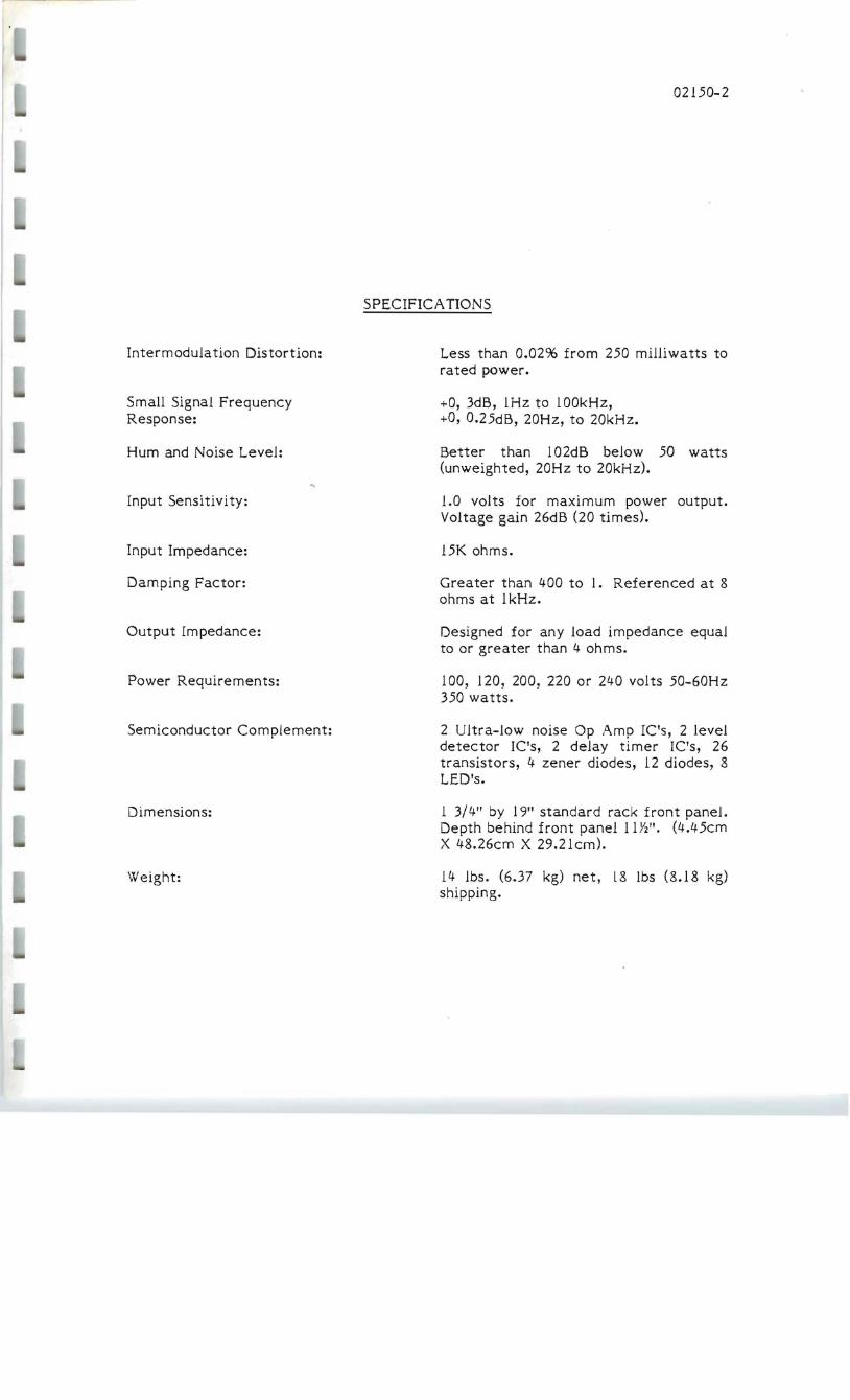
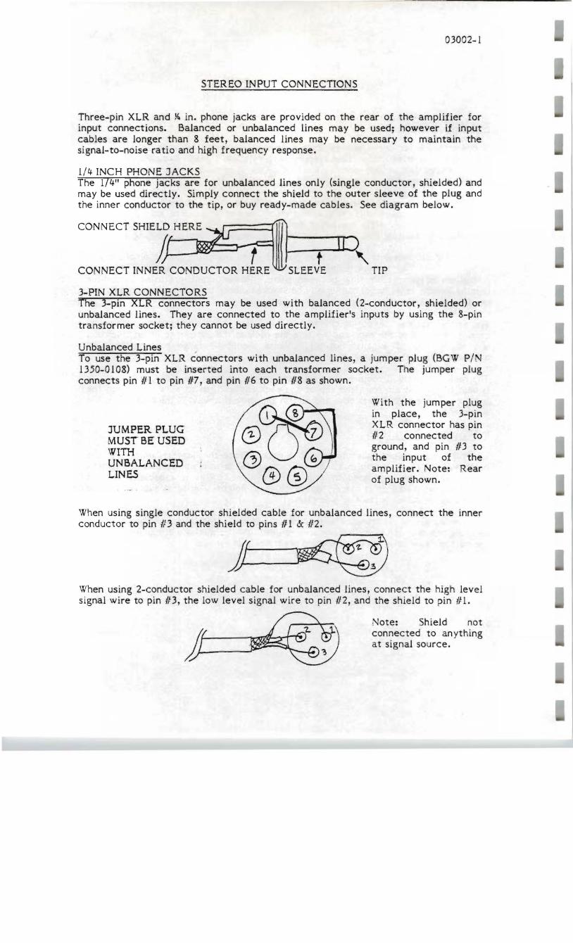
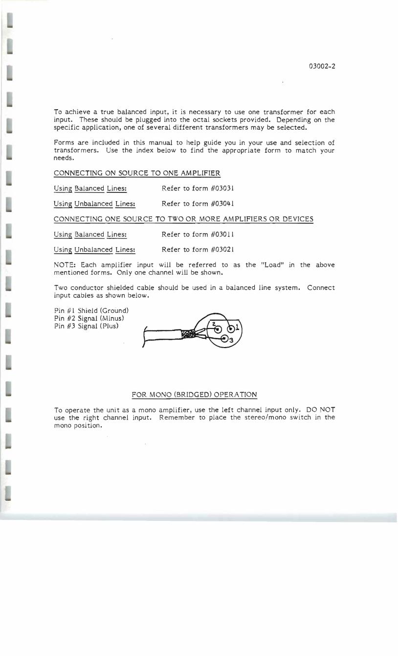
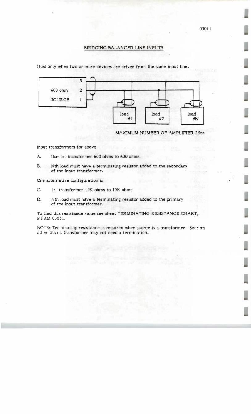
I
r(
load 112
03011
BRIDGING BALANCED LINE INPUTS
Used only when two or more devices are driven from the same input line
r- 3
I
600 ohm 2
W 1 I
SOURCE 1 r---rlt D ~ I--)~ 1000shy
load I load III liN
MAXIMUM NUMBER OF AMPLIFIER 25ea
Input transformers for above
A Use 1 1 transformer 600 ohms to 600 ohms
B Nth load must have a terminating resistor added to the secondary of the Input transformer
rOne alternative configuration is
C l 1 transformer 15K ohms to 15K ohms
D Nth load must have a terminating resistor added to the primary of the input transformer
To find this resistance value see sheet TERMINATING RESISTANCE CHART MFRM 03051
NOTE Terminating resistance is required when source is a transformer Sources other than a transformer may not need a termination
03021
BRIDGING UNBALANCED LINE INPUTS
Used only when two or more devices are driven from the same Input line
600 ohm HI ~~------~------------~--------~
SOURCE LO
load 111
load 112
load liN
The Nth load should have a terminating resistor added to its octal plug between pin 1 and pin 6
To find this resistor value see sheet TERMINATING RESISTANCE CHART MFRM 03051
NOTE Terminating resistance is required when source is a transformer Sources other than a transformer may not need a termination
03031
BALANCED LINE INPUT
Used only when one amp~ifler is driven from one source
600 ohm _ - - ( ) LOAD
Source -I
Input transformer for above
A Use 15 transformer 600 ohms to 15K ohms
NOTE No 600 ohm TERMINA nON IS REQUIRED
B Alternate transformer
Use 1 transformer 600 ohms to 600 ohms
NOTE 600 ohms termination is required on the secondary of the transformer
NOTE Terminating resistance is required when source is a transformer sources other than a transformer may not need a termination
600 ohm termination when required can be accomplished by soldering the resistor across pins 1 and 6 of the transformer as shown below
600 6HMS
or by installing the resistor in a 14 phone plug and inserting it into the unused unbalanced input jack
03041
UNBALANCED LINE INPUT
Used only when one amplifier is driven from one source
600 ohm 1
LOAD I
- - Source
A 600 ohm terminating resistor-- must be added to its octa plug
Between pin 1 and pin 6
NOTE Terminating resistance is required when source is a transformer Sources other than a transformer may not need a termination
600 ohms
03051 middot
TERMINATING RESISTANCE CHART
How to find terminating resistance for balanced or unbalanced 600 ohm lines driving more than one amplifier
STEP A Input Impedance of Amplifiers = Total Load ImpedanceNumber of Amplifiers of Amplifiers
STEP B Total Impedance of Amplifiers - 600 K (Impedance=Factor)
600
STEP C ( t+~ x 600 ohms = Load Resistor Required
EXAMPLE Input Impedance of Amplifiers = 15000 ohms Number of Amplifiers = 4
A 1~000 = 3750 ohms
B 3750-600600 = 525
1C 525 +1 x 600 = 119 x 600 = 71429 ohms
Closest value is 715 ohms 1 metal film resistor
Note all amplifiers must have the same input impedance If not use formula below
i = Total Load Impedance
EXAMPLE Four (4) Amplifiers with input impedance of 15k
30k 30k and 75k
1 = 3750 ohms
I -t IS( + 30~ + 30K -7SK
0301-1
STEREO 0UTPUT CONNECTIONS
Two sets of five-way binding posts on the rear pane serve as output connectors with one black and one red binding post fOl eadl channel Left channel leads go to the blnding posts marked LEFT right channel to those marked RIGHT
Output leads are best connected to the amplifier with standard banana plugs however the five-way action of the binding posts permits the use of tinned wires or spade lugs
Make certain that the speakers are properly phased Connect the black or minus (-) terminal on the speaker cabinet to the appropriate black binding post on the amplifier Connect the red or plus (+) terminal to the red binding post Check to see that the stereQ-mono switch on the rear of the amplifier is in the stereo position
SPEAKER PROTECTION
All speakers can be damaged by having too much power applied to them Fuse protection is an effective- and inexpensive way of preventing this from occurring Ii your speaker system- does not contain a fuse or a circuit breaker a fuse should be placed in series with each speaker and the wire going -~o the red terminal on the rear of -the amplifier bull - shy
Maximum protection can be obtained with fast-acting fuses - Use the value recommended by the manufacturer Ii no value is specified use the chart provided to select the correct value (MFRM-03530)
To use the chart take a straightedge such as a ruler and line up the speakers impedance with its peak music power rating The proper fuse value can then be read from the center column Choose a fuse that is closest to and below the value indicated
WIRE SIZE AND DAMPING FACTOR
The high damping factor ot BG W ampiiiiers results in a very dean bass response Excessively long and small diameter speaker wires can lower the damping factor and distort the lower frequencies A damping factor of at least 50 should be maintained to insure good audio quail ty
The relationship between wire length and diameter and damping factor can be calculated using the chart (MFRM-03510) on the following page Proceed as follows
1 Using a straight-edge line up the gauge of the speaker wire with its length Mark ofi the resulting source resistance where this line crosses the center column
2 Line up the source resistance determined in step III with the manuiacturers impedance ot the speaker system The damping factor can now be read
03501-2
+The impe-1ance of a speaker sys-rem can be approximated by measuring the resistance across the speaker terminals wit1 the amplifier disconnected Multiplying this result by 133 gives you the approximate impedance
Note This method cannot be used with electrostatic speaken
bullbull
-l Is AHNIAUD LOAO SOUacl COltPO
lI51STAHCI ISISlANeI WIbullbull t_1 t_eI taneeeftl tAwet
shy1-IS
OAMfltNG lO
ACTOil
ISO 21_ JOO
2-lt CAaU
SO
IS 20
SOURCE RESISTA1lCE AND DAMPING FACTOR VS LENGTH AND SIZE OF OUTPUT LEADS
MFRM - 03510
-28
20
1
5
bull
12
1 l
16 A
~ 20
2 25
J5
30
00
300
200
150
lao ao
60
0 30
1 20
15 PEAK I
10
bull MUSIC
POWER (watts
6
4
3
2
15
SPEAKER l FUSE SPEAKER () (
EXAMPLE ~z 8n PEAl( POWER = 15 OW Al~SWER FUSE = 2 NIPS
FUSE SELECTOR NOHOGRAPH FOR LOUDSPEAKER PROTECTION
MFRM -03530
03650
MONO OPERATION
The output power of the amplifier can be increased by operating it in the mono (bridged) mode The correct procedure for mono operation is as foHows
1 Set Stereomono switch to mono position
2 Use lett channel input only DO NOT use the right channel input
3 Connect the output across the two red binding posts DO NOT use the black binding posts DO NOT reference the load (speaker) to ground Designate the left channel red binding post (+) and the right channel red binding post minus (-) Fuses when necessary should be placed in series with one red binding post
RIGHT LEFT
STEREO RIGHT LEFT
I ~UT-Iiei I II I
I = I ~N~L~J MONO MAKE OUTPUT CONNECTION
TO RED BINDING POSTS SET SWITCH TO AONO POSITION
MAKE INPUT CONNECTION TO LEFT CHANNEL INPUT
NOTE Minimum load impedance for mono operation should be 8 ohms
CIRCUIT DESCRIPTION
In the mono mode the output at the left channel is fed into the inverting input of the right channel The two channeis work opposite each other when one goes positive the other goes negative thus doubUng the output voltage swing The single output is referenced between the two red binding pOSLs
04000
POWER MAINS CONNECTIONS
The unit should be plugged in only when it has been established that it is wired for the correct power mains voltage and after all other connections have been made
The mains (AC line) voltage is indicated on the label on the rear of the unit Products supplied for use in the United States and Canada are factory wired for 120 volts Only the indicated mains voltage should be used If the mains voltage must be changed see POWER MAINS VOLTAGE CONVERSION
A molded parallel blade U-ground plug is supplied This connector is standard in the United States and Canada For use elsewhere the plug must be replaced with the correct connector The color-code of the cord is as follows
HI (switched Leg) - Brown (or Black) LO (neutral Leg) - Blue (or White) EiR TH (chassis ground) - Green with Yellow tracer (or Green)
OPERATION
PRECAUTIONS
1 Speaker destruction is often due to improper equipment operation This often occurs when someone without the proper appreciation for the components of a high power high quality music system has the opportunity to change records or adjust levels The best protection here is caution Keep the equipment out of reach of untrained adults and children Make sure the speaker is properly protected with fuses (Output Connections Section)
2 Never parallel the two amplifier outputs together
3 When driving any load with an impedance of less than 4 ohms the load should be isolated from the amplifier with a series capacitor in order to avoid both damage to the load and wasting of output power
4 If the amplifier continuously blows fuses something is wrong - do not increase fuse size
5 Do not connect an input ground lead to an output ground lead to do so may cause a ground loop and oscillations
6 Do not operate the amplifier from power mains which exceed the indicated mains voltage by more than lO
7 Never connect the output of the am plifier to another power source such as a ba ttery or power main
8 Do not expose the amplifier to corrosive chemicals such as lye soft drinks salt water etc Also never immerse the amplifier in any liquid
9 Do not remove the amplifiers cover during operations
10 The amplifier is not intended for high frequency-high power use and should not be used for high power at above 20 kHz
11 Neither the amplifier nor any of its leads should be exposed to areas likely to be struck by lightning
PROCEDURES
After all connections have been made to the power amplifier turn the gain controls fully counter-clockwise Turn on the preamplifier then turn on the power amplifier The LED over the circuit breaker or marked IDLE should light If it does not check to see that the amplifier is plugged in to a live power outlet
05200-2
With the preamplifer gain controls fully off advance the left and right power amplifier gain controls about half way clock-wise (slit in knob facing upwards) There ahould be no audible hum if a hum is heard check the connections between the power amplifier and preamplifier Now advance the preamplifier gain controls untiJ the desired maximum volume is achieved Should the preamplifier gain control be in excess of the 34 setting decrease it to half volume and increase the gain controls of the power amplifier to the desired level
Often turn-on transients originate in the pre-amp or tuner This is especially true of tube-type units If this situation arises turn the amplifier on after the other units have had adequate time to stabilize
12310
150 CIRCUIT DESCRIPTION
Both channels of the amplifier operate in the same manner and only the left channel will be explained
POWER SUPPLY
The AC input power from P501 passes through the Circuit breaker CB 301 From CB 301 the AC goes to the power transformer T301
The output of T301 goes to a full wave bridge rectifier capacitor input filter circuit consisting of 0301 C302 and C303 to give a positive and negative power supply voltages
AMPLIFIER
The input signal from J 301 is applied to the R301 input level control The output from R301 is applied to the inverting input (pin 2) of op amp IC 103 through the coupling network CI0l RI01 CI02 and RI04 This network provides a high impedance to the amplifier and filters out DC and radio frequency interference
QI03 and QI04 divide the signal into positive and negative components respectively They are connected common emitter and provide voltage gain QII0 and Ql1l are connected common collector to provide the current gain necessary to drive the output stages Q 112 and Q 113 The output appears across fly back clipping diodes 0103 and 0104 then passes through compensation networks LlOlR128 and R130C1l7 and thermo switch 5101 to appear at output jacks J308 Switch 5101 opens if the output transistors reach 100 degrees C
To maintain overall stability linearity and low distortion degenerative feedback is used throughout the amplifier Voltage divider R 103C 106 and R 106 applies the correct amount of feedback to the non-inverting input (pin 3) of op amp IC 103 Except for the input the amplifier uses direct coupling throughout Q 106 and Q 107 provide the current limiting necessary to protect the output stage
BRIDGED MODE
When the monostereo switch 5301 is set to mono it converts the right channel amplifier to a unity gain inverting power amplifier
5301 tvlonoStereo switch grounds the normal input to the right channel and connects the output of the left channel amplifier to drive the right channel sum ming point RIO 2
I I t
~ -1
1-
w bull10 bull
I
v-a
_L
it-
Il1 -I~
1 )~-
0 ~ ~
~ ru
I~t
t~C14middot bull 11amp rc bull ~ bullbull___-+-_
CO
~1~t
-Jfl~L I~ lP-f~
1-
~Lmiddotf ~ I ~
cJPI
100
1-lt
4gt1
~II ~( a
i ~)
11 Q
r~
1 ~-O- I
IOn
I t I
~I
J16 I
~
01 fI~Or
I
I I I
I I
I
t
i I
NOTES Ut-ll ESSOIII(IIWISE SPfClnEO
bull t~I~J~(middotmiddotmiddotmiddotmiddot
QS IY r~ so I t
gt 1 0I 1
- _I
IIHlln OtllRWlU srorolD BGWSYSIEMS 13130 SOUlIlYlJKOIIIIIIIE
O_HSIOttttQ NtD 0l(AAHCampHQ tIAWlllOIINECA 9O50 n - 1IJI9738090POI~ YIIS W
HllONl bullbull III nltCIIU IIIWII 5D 6~~Tlt IIpoundr~~t PLY AnLR rUII1IlPRELIMINARY alleo(IlIUIlAHCI Ole 5 JD( bull oJ J()IX bullbull1 fOl(aJrf1Ct ON AIGUS _ bullbullbullbullDOCUMENT bull UK SlIM (nGll lUO totAl
flEVsoatAtl IIIlIJOIOHl 55 Ie-
FOA REFERENCE ONLY
DO NOr Ir ORAwllOCl
-----
------
R[VISIONS u ppAOVlOOlsatrlOC 0(
Clffol - shy -i bull - Gmiddotmiddot
fL
- shy~-J ~ 91ut ~~-=
I amp I
~ __ t
oo~ p-- ~t(L)
Pry J- ~~
tLLi ~
cpound
)
11113~ IJHIUS OlllERWlst S(ctmD
11~3 1- 01[5000 0 lOl[AAlOC1tO (0 (lSAS YIU
ptUpoundHUlHS AIII( IN tCH(s
(= [~c7~
I XI( == OJ DJ( - 2 010 lOlflllAHC( Oft AtlGlU J Omiddot bull
81(M SIAP (ocrs YoU
SIIfAC[ ft()UG~US Ie- 1
NOT E S UNLESS 011 EIWISE SPEClf lEO----i DO ~o Sr
bull ~~t~-middot~~ n-r
1 rL VIgt bull~1 (D
~ ~ I
~~~_llULL I Ilttl
~ __ I lOOe p-n ~f(pound)
1
--IL J P~lt
Iii I Ii
tl-ol G-
T 0 -lb1gt
~ +Icc
50)
IJ 7~ -t~
shyPRELIMINARY DOCUIVIENT
FOR REFERENCE ONLYW BGWSYSIEMS
-1_ -~LLV
~I~ i I OO - II t1S I
llt-flOgt
IlJt~8iigp~~t~~~Evr 12131913 B090
(IfIAWlt IU
tv IIJ CIsssCiilCK--- --- 5b
DltAWO 00( A nEV J37D
~ l( ORAWIlIO
I
t-c~
6U (IV )
-ZOV
~
0 6dI ltgt~t- 6coJ
7
Cgtv(w-)
I()O V
~1UJifJ
6ur
Bv(lJ-
-ztfOV
NOTES ur ES501~nWISE SPEClflm 00 riOT SCN [ ~V1Ha
R[VISIONS
Ull O(SCIIIKlH DAl( AlPnOV(O
) baJ-~~ 0 sect~) ~
rh ~ 3 ~
-zoov
-=9 )ti6L1 - -~-----0 -shy - cshy
rt7
PRELIMINARY DOCUMENT
FOR REFERENCE ONLY
220V
UHll$S 01 H(RWIS[ snCIUfO
OIM(HSIONltfC AND 100VlNfCIHO r tSA$1 YIU
UMOtSIOH5 Nt( Iii IIfCti(S AtIO APPlt ATTU PlArtHO
rouflulaquol Off ()(CU-I Ja Ell t J)J JIXIl = 010
JOl(llHC( ON AHGlU a lD
IUA Slwtr (1)((5 bull 10 MAJ
IUlfAC[ ROtKOtipoundS5 Ie
tRofCI (Hajj
Ll
SIll
c SCA(
tUJ~ ISb
L-__ shy-r
~--- cshy -shy(~
~
2-_
IlGW~Y5EMS 13130 OUllt YlJI(ON AVE tiW tOt INECA 9025f1 12131913middot8000
L0lfl ~( Fc Dot-Egt Ie (rpoundE 1610-
Ico ( 116~ S OAAWIIKI NUItAMIII
- -lt3t()
SltUl l
BGW SYST~~S INC
ENG NO DESCRI~TlaN PART NO
PARTS iIST 150 ~ 12390
SCHEMATIC AC wIRIN~ MFR~ 12360 SCHEMAT[C CHASSIS MFRM l2370 SCHEMATIC HEATS[NK MFRM 12380 B~OCK ~IAGRAM MFRM 12390
A~L COMPONENTS _ITH DESIGNATIONS IN THE 200 SERIES ARE RIGHT CHANNEL HEATSINK NUMBERS - ~EFER Ta 100 SERIES NUMBERS EXAMPL~ 201 ~aULD BE THE SAME AS CIOl
CAPACITORS
1gt1 47 UF 2SV TANTALUM CI02 240PF SUOII MICA CI03 10PF 10011 MICA CI04 30 PF 50ull1 CA CI05 47UF 10V E~ECTR~~YTIC CLOt) 30PF SOu II ~ICA
Clgt7 12UF 10011 META~IlE) ~YLAR
(lO~ 12UF 10011 META~IlEJ MYLAR CI0 220PF 500 DISC C 1 1 ) lUF 2511 JISC ell 1 lOOOPF 50011 DISC (112 1000PF 5001 DISC C113 S60PF 5uOll MICA C 1 14shy 240PF 50011 MICA Cl15 l2uF 10011 ~ETA~IlEJ ~YLAR Cl15 12uF 10011 METALILEJ MYLAR Cl17 12UF 100V METAiIlEJ MYLAR Cl1 1UF 25 )I5C Cll~ bull 1 UF 2511 J I SC C12) 1UF 2511 JISC 121 015UF 10011 MYLAR C122 1UF 25 JISC (123 47uF 10011 META~ILEJ ~YLA~ C 12+ 1UF 2511 )IiC C125 430PF 100 IICA C12l tUF 2511 DISC C301 OlvF 50011 DISC C302 8500UF SOli E~ECTRQLtTIC
C3gt3 8500UF 501 ELECTqQLtTIC C304shy 01UF 25 JISC C3JS OluF 25V JISC
0226-0005 0090-0240 0060-0010 0060-0030 0456-0047 0060-0030 0363-9003 0363-8003 0100-0220 0129-0100 0100-1000 0100-1000 0080-0560 0090-0240 0363-8003 0363-8003 0363-8003 0129-0100 0129-0100 0129-0100 0369-0015 0129-0100 0363-3000 0129-0100 0060-0430 0129-0100 Ot99-0100 0533-IJOOd 0533-0008 0129-0100 0129-0100
ENG NO
=gt101 0102 )103 01 +
~1S 0100 ) 107 ~10j
~3Jl
rcia 1 IC1J2 r C 103
J 1 J 1
J301 J302 J3JJ J 3J 4
J305 J30~
J307 J30~
J30~
J310 J311
1 0 1
P3J1 PJOZ
JIJ1 0102 0103 01J4 (HOS
01)6 0107
12390-2
BGw SYSTEMS lNC
OESCRIPT[J~
DIODES PART 0
IN41461N914 OI~DE IN414d1N914 DIODe IN400~ DIJDE lA 400V IN4004 DIJDE lA 4QOV lN4740A IOV ZENER DIODE IN4740A IOV ZEN~R DIODE 1N414d1N914 DIODE IN41481N914 DI~Dc B~IDGE RECTFIE~ ~Brl2502
1900-4148 1900-4146 1900-4004shy1900-4004 1900-4740 1900-4740 1900-414d 1900-4148 1886-2502
INTEGRATED CIRCU[TS
LEVEL DETECTOR TI~ER ~~555
OP AMP NE5534
TL0467CP 1685-0487 18d5-0555 1685-5534
JACKS
MOLEX 12 ~IN CO~NECTOR 03-09-2121 INPuT JAClt Nlll r NPU r J A Clt Nil 1
6 PIN SQCtltET 6 PIN SOCKET 3 PIN XLR PC ~O~NT 3 PIN XLR ~C MOUNT STE~EO PH~NE JACK 39 BUSHING CJNNECTQR 3INDI~G POST RED CONNECTOR 3INDr~G POST RED CJNN~crOR 3IN~I~G POST BLACK CONNEcrOR 3INDI~G POST BLACK
1231-2121 9999-0111 9999-0111 1203-0006 1203-0008 1205-0002 1205-0002 1205-0005 1231-0008 1231-0008 1231-000~
1231-0009
I ~DUCTOR S
14JH INDUCTOR 22GA MIRE 8022-0400 SEE R128 1700-0001
PLUGS
MOLEX MOL~X
12 12
~IN ~O~NECTOR 03-09-1126 ~IN CO~NECTOR 03-09-1126
1231- 1 1 26 1231-1126
TRANSISTORS
2N2484 NPN SI~ICON LOW SIGNAL r09~
MJE lSO~8 rRANSISTOR NPN r0220 MJE 350 PNP r~ANSlsrOR
MJE J~O NP~ T~A~SISTOR
MJE 720 N~N rRA~SISTOR
2N4401 NPN 5r~ICON LO~ SIGNAL r092 2N4403 PNP SI~ICON LO~ SIGNAL rU92
1654-2484 1854-5028 1953-1) 350 1954-0340 l854-0720 l654-440 1 1853-4 03
123903
8G- SYSTEMS INC
ENG N) 01 Js 010~
0110 ) 1 1 1 ell 12 0113
Q10l ~lJ2
~ 1 J 3
RI04shy
U 15
RlelS ~107
HD~
~lel~
~110
~ 1 1 1 ~ 11 2 R113 en 1 4shy
~ 115 lt1 1 ~ R 11 7 ~11i
R 1 1
R12J ~ 1 2 1
~122
en 23 ~124-
~125
~12)
~127
~12j
~121
~13()
R131 ~132
R133 R134 R135 R13S R137 R138 R13~
R14J R 1 ~ I
Rl~2
DESCR1TI31 4JE 340 N)N THAlS 1 STO~ MJE 350 PNP TRAt4SISTOR MJ E 15028 NPN T~ANSISTOR T0220 MJE 15029 PNP TRANSISTOR T0220 MJ 15022 NPN TRANSISTOR T03 MJ 15023 ~P T~1SISTOR T03
RESISTORS
47K 5X 12~ DEPQSITED CAR~ON 475K IX ~ETA~ FI~M 475K 1~ ~ETA~ FI~M
~7K 5~ 12~ DEPOSITE~ CARBON 47K 5X 12w DEPOSITED CARBON 24~K 1~ META~ FI~M
100~ 5 12~ DEPOSITE3 CARBON 15K 5 12WDEPuS1TED CARBON 15K 5~ 12~ DEPOSITED CAR~ON 0~0~ 5 12w DEPOSITE3 CARBON odOR 5 12M DE~OSITEJ CARBON o~R 5 12~ DEP~SITED CARBON 1JOR 5 12~ DEQO~ITE3 CARBON FACTORY SE~ECTEJ aFFSET ADJUSTMENT 27~ 5 1211 0E~OSITED CARBUN 470R 5 12~ DEOSITE) CARBON FACTORV SE~ECTE3 alAS ADJUST~ENT 100R 5 12~ DE~OSITEJ CARBON 100R 5~ 12~ DE~OSITEJ CARBON 1~ 5 12M DEPOSITE3 CARBON 1~ 5 12 DEPOSITED CARBUN 100R 5 12 DEPOSITE) CARBON 100R 5 12 DEOSITEJ CARBON 27R 5 2 wIRE laquoOUlD BIIIH 27~ 5 2M MIRE OU~D 8~H
O 1~ 5 211 IRE wOUND BwH O 1 R 5 2M If I HE IOUND 8wH ~ () R lOX 2M CARB)N COMP SEE ~101 270R 10~ 2~ M 1 RE MOUND SIIIH 33R lOX 2M MI~E ~OUND BWH 820R 3~ WI~E WOJNO 27lt 5~ 12~ DE~OSITEJ CARBON 24K 5~ l2 DEPOSIT~D CARBON 47K 5 12~ DEPOSIT2D CAR80N 100lt 5~ 12 OEPO~ITEJ CA~80N 1~ 5 12~ DEPOSITED CARBON 820R 5~ 12w OEOSITE3 CARBUN 10K 5~ 12~ DEPQSIT~D CARSON 39~ 5~ 12A DE~OSITE) CARBON 100lt 5 12w DEPOSITED CARBUN 10K 5~ l~W DEPOSIT~D CARBON 3~lt 5X 12~ OE~osrTEJ CARBON
PART 40
1854-0340 1853-0350 1854-5028 1853-5029 1854-1522 1853-1523
5005-4703 5001-4752 5001-4752 5005-4702 5005-4702 5001-2491 5005-1002 5005-1503 5005-1503 5005-0801 500 5-6d 01 5005-0800 5005-1002
5005-2702 5005-4701
5005-1002 5005-1002 5005-1003 5005-1003 5005-lU02 5005-1002 4025-2070 4025-2070 4025-1009 4025-1009 6020-1001
4020-2701 4020-3300 4030-8201 5005-2702 5005-2403 5005-4703 5005-1005 5005-1006 5005-3201 5005-1004 5005-3902 5005-1005 5005-l004 5005-3902
12390-4
aG~ SYSTMS INC
NG NO DESCRlTION PART 140
~143 2JOR 5 12M DEOSITE) CARBON 5005-2002 R144 2aOR 5 12 DEOSITED CARBON 5005-2002 R145 82)( 5 14- DEPOSITEgt CAkSON 5065-8202 R14~ 82)( 5 14- ~EPOSITED CARSON 5065-8202 Q3Jl 22K ST~P ATTENUATOR NOSLE 7006-2015 R3J2 22K ST~P ATTENUATOR NOBLE 7006-2015 Q303 27lt 5 2 CARSQN CO~~P 6025-2702
S I TCHES
SlOl T1E~I4A_ SolITCH JOR 212F 0630-3445 53J1 5-IDE SITCH R~CESSEgt HANDLE 0620-1)206
TRiNSFORMERS
T3Jl 0900-0l24
TEiUH NAL 5T~ IPS
Ta30l G~OUND aA~QIER STRI ~STRA 0720-1696
____________ __
WARRANTY REGISTRATION PLEASE FILL OUT AND RETURN THIS CARD WITHIN 2 WEEKS FROM DATE OF PURCHASE
NAME DATE PURCHASED
ADDRESS PHONE
CITY STATE ZIP
PURCHASED FROM DEALER
ADDRESS
CITY STATE ZIP
MODEL NUMBER _________
SERIAL NUMBER _______shy
PURCHASE PRICE ________
FOR WHAT PURPOSE IS THE UNIT INTENDED
HOME STUDIO SOUND REINFORCEMENT OTHER (EXPLAIN)
IS THIS AMPLIFIER A REPLACEMENT FOR AN EXISTING UNIT
I F YES) WHAT KIND ___________________
WHY DID YOU CHOOSE A BGW POWER AMPLIFIER
__DEALER RECOMMENDAT ION _~MAGAZINE ADVERTISEMENT
__SOUND QUAL ITY __TECHNICAL DESIGN
~_OTHER __FRIENDI S RECOMMENDATION
COMMENTS
SYSTEMS middot
13130 SOUTH YUKON AVENUE ~AWTHORNE CALI FORN LA 90250
------~--------------------- ----------_ _------------------------------shyFOLD HERE
----------------
---
SERVICE AtmiORIZATION FORM
PLEASE COMPLETE THIS FORM AS COMPLETELY AS POSSIBLE AlID RETURN TO BGW SYSTEMS BEFORE RETURNING UNIT
NAL1E ---------------- PHONE
ADDRESS (CITY) (STATE) (ZIP)
UNIT -----------------------------------MODEl SERIAL NUMBER
1 DESCRIBE SYMPTOMS
2 bull WHI CH CHANNElS (S ) EXHIB ITS THE PROBlEMS
3 WHAT OTHER EQUIPMENT WAS INVOLVED
MANUFACTURER MODEL NO PREAMP SPEAKERS
4 UNDER 1NHAT CONDITIONS DOES THE PROBLEM OCCUR (CHECK THOSE THAT APPLY)
A ALL THE TL1E ____ B AFTER AWHILE C AT HIGH VOLUME=-LE~VE=L--S-D AT HIGH TEMPERATURES ______ E OTHER (EXPLAIN)
5 HOW OFTEN DID THE PROBLEM OCCUR
6 WHAT DID YOU DO TO ISOLATE THE PROBLEM TO TIlE POwER AMP
7 FURTHER COMMEITS
IT IS MORE ETIEDlUiT TO CALL YOUR DEALER OR OUR FACTORY EXPLAINING THE NATURE OF YOUR PROBLEM IN MAllY INSTANCES THE PROBLEM Campl BE SOLVED WITHOUT RETURNING THE UNIT TO THE FACTORY WARNING TIlE UNIT MUST BE RETURNED IN AN ORIGINAL FACTORY CONTAINER IF YOU DO NOT HAVE ONE WE WILL PROVIDE A REPLACEMENT FOR $1400 FACTORY AUTHORIZED WARRANTY REPAIR STATIONS ARE LOCATED THROUGHOUT THE US CALL YOUR DEALER OR THE FACTORY FOR THE LOCATION OF TIlE SERVICE STATION NEAREST YOU
l3l30 SOUTH YUKON AVENUE
rtAWTHORNEI CALIFQIRrI IA 90250
bull FOUl HERE
middot r POLARI-T-Y --~-- _ v( b INSERTION LOSS
FREQUENCY RESPONSE ~
I shy
-~ --____
CJ lmiddotE ~ shy
I
20 - 20K RESPONSEI 1 shy((i I 600 OHM DRIVER1~syUJJJ 0900-9250 i 1TESTED I3Y 15K NOM LOAD
BRIDGING TRANSFORMER li ~ [ OdB REf15K - 15K V
o
dB 5
10
1000 3 4 5 6 7 B 91~ 2
20000
FREQUENCY IN CYCLES PER SECOND I
----
~ SYSTEMS 50001
------------------------ -- --shy13130 SOUTH YUKON A V ENUE HAWTHORNE CALIFOR N I A 90250
PHONE (213) 9 73-8090 TELE X NO 66- 4 -1 9 4
t-
MODEL 150 TEST EPORT
DA TE_ 1 9l--__1 _ t L C_f1_-__ ~ _ TECHNICIAN C- a 1 (r SERIAL NO_=-_ -- ( l 6_l~---J=--__ _O
LINE VOLT AGE _ __ -=L=---()-_V___
CH 1 CH2 MONO
Power at Clip (0 1 THO) 2- I -V 2 1 r J 7 ( 4- V8 ohms - vol ts out
6W kJ t l)WPower
Power at Clip (015 THO) I R- 4- J4 ohms - volts out PI J ~ 4 W JgtJ 0Power
THO 50 Watts - 8 ohms (20 1 Volts)
06 (20Hz 20kHz 611
Small Signal Bandw idth 8 ohms
- 3dB Freque ncy kHz f1 kHz
Noise Leve l Out put Noise Volt age
mV I 0 1 mV20Hz t o 20kHz
Quiescent Power 4- () Watts
10 5 83
5004-5
BGW Systems - Q A Check List
MODEL If SERIAL NO INSPECTORSIGNA TURE CHECK
15tJ J606
1- Front Panelchassis free of blemishes ~ 2 Knobs correctly aligned and tightened ~ 3 All controls and switches function normally
4- Check for stripped screw heads ~ 5 Correct voltage tag
6 Five-way binding posts tightened and correctly aligned ~ 7 Input jacks wired correctly and tightened ~ 8 Check for correct circuit breaker ~ 9 Check wire harness for neatness and pinched wires ~
lO Check for loose hardware ~
090l83
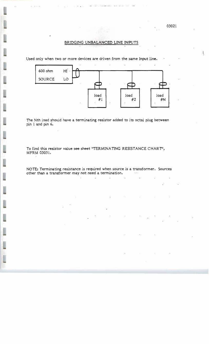
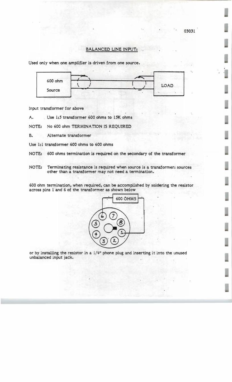
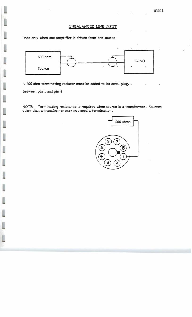
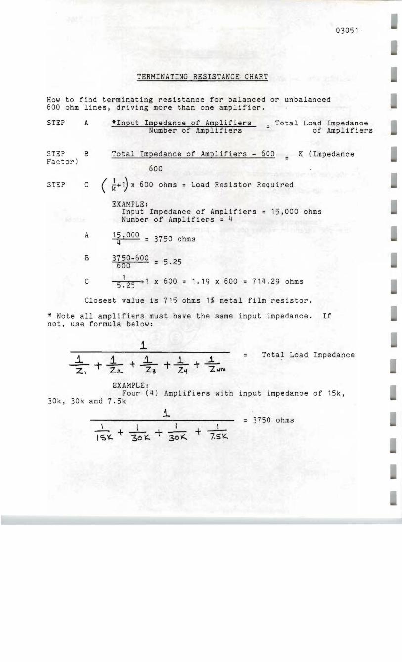
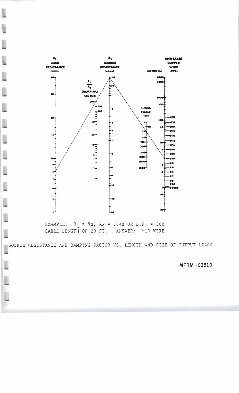
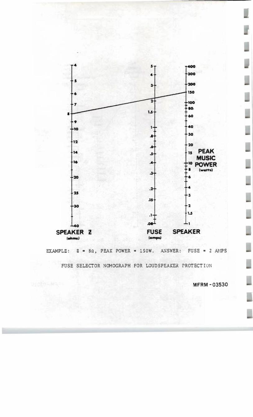
1
5
bull
12
1 l
16 A
~ 20
2 25
J5
30
00
300
200
150
lao ao
60
0 30
1 20
15 PEAK I
10
bull MUSIC
POWER (watts
6
4
3
2
15
SPEAKER l FUSE SPEAKER () (
EXAMPLE ~z 8n PEAl( POWER = 15 OW Al~SWER FUSE = 2 NIPS
FUSE SELECTOR NOHOGRAPH FOR LOUDSPEAKER PROTECTION
MFRM -03530
03650
MONO OPERATION
The output power of the amplifier can be increased by operating it in the mono (bridged) mode The correct procedure for mono operation is as foHows
1 Set Stereomono switch to mono position
2 Use lett channel input only DO NOT use the right channel input
3 Connect the output across the two red binding posts DO NOT use the black binding posts DO NOT reference the load (speaker) to ground Designate the left channel red binding post (+) and the right channel red binding post minus (-) Fuses when necessary should be placed in series with one red binding post
RIGHT LEFT
STEREO RIGHT LEFT
I ~UT-Iiei I II I
I = I ~N~L~J MONO MAKE OUTPUT CONNECTION
TO RED BINDING POSTS SET SWITCH TO AONO POSITION
MAKE INPUT CONNECTION TO LEFT CHANNEL INPUT
NOTE Minimum load impedance for mono operation should be 8 ohms
CIRCUIT DESCRIPTION
In the mono mode the output at the left channel is fed into the inverting input of the right channel The two channeis work opposite each other when one goes positive the other goes negative thus doubUng the output voltage swing The single output is referenced between the two red binding pOSLs
04000
POWER MAINS CONNECTIONS
The unit should be plugged in only when it has been established that it is wired for the correct power mains voltage and after all other connections have been made
The mains (AC line) voltage is indicated on the label on the rear of the unit Products supplied for use in the United States and Canada are factory wired for 120 volts Only the indicated mains voltage should be used If the mains voltage must be changed see POWER MAINS VOLTAGE CONVERSION
A molded parallel blade U-ground plug is supplied This connector is standard in the United States and Canada For use elsewhere the plug must be replaced with the correct connector The color-code of the cord is as follows
HI (switched Leg) - Brown (or Black) LO (neutral Leg) - Blue (or White) EiR TH (chassis ground) - Green with Yellow tracer (or Green)
OPERATION
PRECAUTIONS
1 Speaker destruction is often due to improper equipment operation This often occurs when someone without the proper appreciation for the components of a high power high quality music system has the opportunity to change records or adjust levels The best protection here is caution Keep the equipment out of reach of untrained adults and children Make sure the speaker is properly protected with fuses (Output Connections Section)
2 Never parallel the two amplifier outputs together
3 When driving any load with an impedance of less than 4 ohms the load should be isolated from the amplifier with a series capacitor in order to avoid both damage to the load and wasting of output power
4 If the amplifier continuously blows fuses something is wrong - do not increase fuse size
5 Do not connect an input ground lead to an output ground lead to do so may cause a ground loop and oscillations
6 Do not operate the amplifier from power mains which exceed the indicated mains voltage by more than lO
7 Never connect the output of the am plifier to another power source such as a ba ttery or power main
8 Do not expose the amplifier to corrosive chemicals such as lye soft drinks salt water etc Also never immerse the amplifier in any liquid
9 Do not remove the amplifiers cover during operations
10 The amplifier is not intended for high frequency-high power use and should not be used for high power at above 20 kHz
11 Neither the amplifier nor any of its leads should be exposed to areas likely to be struck by lightning
PROCEDURES
After all connections have been made to the power amplifier turn the gain controls fully counter-clockwise Turn on the preamplifier then turn on the power amplifier The LED over the circuit breaker or marked IDLE should light If it does not check to see that the amplifier is plugged in to a live power outlet
05200-2
With the preamplifer gain controls fully off advance the left and right power amplifier gain controls about half way clock-wise (slit in knob facing upwards) There ahould be no audible hum if a hum is heard check the connections between the power amplifier and preamplifier Now advance the preamplifier gain controls untiJ the desired maximum volume is achieved Should the preamplifier gain control be in excess of the 34 setting decrease it to half volume and increase the gain controls of the power amplifier to the desired level
Often turn-on transients originate in the pre-amp or tuner This is especially true of tube-type units If this situation arises turn the amplifier on after the other units have had adequate time to stabilize
12310
150 CIRCUIT DESCRIPTION
Both channels of the amplifier operate in the same manner and only the left channel will be explained
POWER SUPPLY
The AC input power from P501 passes through the Circuit breaker CB 301 From CB 301 the AC goes to the power transformer T301
The output of T301 goes to a full wave bridge rectifier capacitor input filter circuit consisting of 0301 C302 and C303 to give a positive and negative power supply voltages
AMPLIFIER
The input signal from J 301 is applied to the R301 input level control The output from R301 is applied to the inverting input (pin 2) of op amp IC 103 through the coupling network CI0l RI01 CI02 and RI04 This network provides a high impedance to the amplifier and filters out DC and radio frequency interference
QI03 and QI04 divide the signal into positive and negative components respectively They are connected common emitter and provide voltage gain QII0 and Ql1l are connected common collector to provide the current gain necessary to drive the output stages Q 112 and Q 113 The output appears across fly back clipping diodes 0103 and 0104 then passes through compensation networks LlOlR128 and R130C1l7 and thermo switch 5101 to appear at output jacks J308 Switch 5101 opens if the output transistors reach 100 degrees C
To maintain overall stability linearity and low distortion degenerative feedback is used throughout the amplifier Voltage divider R 103C 106 and R 106 applies the correct amount of feedback to the non-inverting input (pin 3) of op amp IC 103 Except for the input the amplifier uses direct coupling throughout Q 106 and Q 107 provide the current limiting necessary to protect the output stage
BRIDGED MODE
When the monostereo switch 5301 is set to mono it converts the right channel amplifier to a unity gain inverting power amplifier
5301 tvlonoStereo switch grounds the normal input to the right channel and connects the output of the left channel amplifier to drive the right channel sum ming point RIO 2
I I t
~ -1
1-
w bull10 bull
I
v-a
_L
it-
Il1 -I~
1 )~-
0 ~ ~
~ ru
I~t
t~C14middot bull 11amp rc bull ~ bullbull___-+-_
CO
~1~t
-Jfl~L I~ lP-f~
1-
~Lmiddotf ~ I ~
cJPI
100
1-lt
4gt1
~II ~( a
i ~)
11 Q
r~
1 ~-O- I
IOn
I t I
~I
J16 I
~
01 fI~Or
I
I I I
I I
I
t
i I
NOTES Ut-ll ESSOIII(IIWISE SPfClnEO
bull t~I~J~(middotmiddotmiddotmiddotmiddot
QS IY r~ so I t
gt 1 0I 1
- _I
IIHlln OtllRWlU srorolD BGWSYSIEMS 13130 SOUlIlYlJKOIIIIIIIE
O_HSIOttttQ NtD 0l(AAHCampHQ tIAWlllOIINECA 9O50 n - 1IJI9738090POI~ YIIS W
HllONl bullbull III nltCIIU IIIWII 5D 6~~Tlt IIpoundr~~t PLY AnLR rUII1IlPRELIMINARY alleo(IlIUIlAHCI Ole 5 JD( bull oJ J()IX bullbull1 fOl(aJrf1Ct ON AIGUS _ bullbullbullbullDOCUMENT bull UK SlIM (nGll lUO totAl
flEVsoatAtl IIIlIJOIOHl 55 Ie-
FOA REFERENCE ONLY
DO NOr Ir ORAwllOCl
-----
------
R[VISIONS u ppAOVlOOlsatrlOC 0(
Clffol - shy -i bull - Gmiddotmiddot
fL
- shy~-J ~ 91ut ~~-=
I amp I
~ __ t
oo~ p-- ~t(L)
Pry J- ~~
tLLi ~
cpound
)
11113~ IJHIUS OlllERWlst S(ctmD
11~3 1- 01[5000 0 lOl[AAlOC1tO (0 (lSAS YIU
ptUpoundHUlHS AIII( IN tCH(s
(= [~c7~
I XI( == OJ DJ( - 2 010 lOlflllAHC( Oft AtlGlU J Omiddot bull
81(M SIAP (ocrs YoU
SIIfAC[ ft()UG~US Ie- 1
NOT E S UNLESS 011 EIWISE SPEClf lEO----i DO ~o Sr
bull ~~t~-middot~~ n-r
1 rL VIgt bull~1 (D
~ ~ I
~~~_llULL I Ilttl
~ __ I lOOe p-n ~f(pound)
1
--IL J P~lt
Iii I Ii
tl-ol G-
T 0 -lb1gt
~ +Icc
50)
IJ 7~ -t~
shyPRELIMINARY DOCUIVIENT
FOR REFERENCE ONLYW BGWSYSIEMS
-1_ -~LLV
~I~ i I OO - II t1S I
llt-flOgt
IlJt~8iigp~~t~~~Evr 12131913 B090
(IfIAWlt IU
tv IIJ CIsssCiilCK--- --- 5b
DltAWO 00( A nEV J37D
~ l( ORAWIlIO
I
t-c~
6U (IV )
-ZOV
~
0 6dI ltgt~t- 6coJ
7
Cgtv(w-)
I()O V
~1UJifJ
6ur
Bv(lJ-
-ztfOV
NOTES ur ES501~nWISE SPEClflm 00 riOT SCN [ ~V1Ha
R[VISIONS
Ull O(SCIIIKlH DAl( AlPnOV(O
) baJ-~~ 0 sect~) ~
rh ~ 3 ~
-zoov
-=9 )ti6L1 - -~-----0 -shy - cshy
rt7
PRELIMINARY DOCUMENT
FOR REFERENCE ONLY
220V
UHll$S 01 H(RWIS[ snCIUfO
OIM(HSIONltfC AND 100VlNfCIHO r tSA$1 YIU
UMOtSIOH5 Nt( Iii IIfCti(S AtIO APPlt ATTU PlArtHO
rouflulaquol Off ()(CU-I Ja Ell t J)J JIXIl = 010
JOl(llHC( ON AHGlU a lD
IUA Slwtr (1)((5 bull 10 MAJ
IUlfAC[ ROtKOtipoundS5 Ie
tRofCI (Hajj
Ll
SIll
c SCA(
tUJ~ ISb
L-__ shy-r
~--- cshy -shy(~
~
2-_
IlGW~Y5EMS 13130 OUllt YlJI(ON AVE tiW tOt INECA 9025f1 12131913middot8000
L0lfl ~( Fc Dot-Egt Ie (rpoundE 1610-
Ico ( 116~ S OAAWIIKI NUItAMIII
- -lt3t()
SltUl l
BGW SYST~~S INC
ENG NO DESCRI~TlaN PART NO
PARTS iIST 150 ~ 12390
SCHEMATIC AC wIRIN~ MFR~ 12360 SCHEMAT[C CHASSIS MFRM l2370 SCHEMATIC HEATS[NK MFRM 12380 B~OCK ~IAGRAM MFRM 12390
A~L COMPONENTS _ITH DESIGNATIONS IN THE 200 SERIES ARE RIGHT CHANNEL HEATSINK NUMBERS - ~EFER Ta 100 SERIES NUMBERS EXAMPL~ 201 ~aULD BE THE SAME AS CIOl
CAPACITORS
1gt1 47 UF 2SV TANTALUM CI02 240PF SUOII MICA CI03 10PF 10011 MICA CI04 30 PF 50ull1 CA CI05 47UF 10V E~ECTR~~YTIC CLOt) 30PF SOu II ~ICA
Clgt7 12UF 10011 META~IlE) ~YLAR
(lO~ 12UF 10011 META~IlEJ MYLAR CI0 220PF 500 DISC C 1 1 ) lUF 2511 JISC ell 1 lOOOPF 50011 DISC (112 1000PF 5001 DISC C113 S60PF 5uOll MICA C 1 14shy 240PF 50011 MICA Cl15 l2uF 10011 ~ETA~IlEJ ~YLAR Cl15 12uF 10011 METALILEJ MYLAR Cl17 12UF 100V METAiIlEJ MYLAR Cl1 1UF 25 )I5C Cll~ bull 1 UF 2511 J I SC C12) 1UF 2511 JISC 121 015UF 10011 MYLAR C122 1UF 25 JISC (123 47uF 10011 META~ILEJ ~YLA~ C 12+ 1UF 2511 )IiC C125 430PF 100 IICA C12l tUF 2511 DISC C301 OlvF 50011 DISC C302 8500UF SOli E~ECTRQLtTIC
C3gt3 8500UF 501 ELECTqQLtTIC C304shy 01UF 25 JISC C3JS OluF 25V JISC
0226-0005 0090-0240 0060-0010 0060-0030 0456-0047 0060-0030 0363-9003 0363-8003 0100-0220 0129-0100 0100-1000 0100-1000 0080-0560 0090-0240 0363-8003 0363-8003 0363-8003 0129-0100 0129-0100 0129-0100 0369-0015 0129-0100 0363-3000 0129-0100 0060-0430 0129-0100 Ot99-0100 0533-IJOOd 0533-0008 0129-0100 0129-0100
ENG NO
=gt101 0102 )103 01 +
~1S 0100 ) 107 ~10j
~3Jl
rcia 1 IC1J2 r C 103
J 1 J 1
J301 J302 J3JJ J 3J 4
J305 J30~
J307 J30~
J30~
J310 J311
1 0 1
P3J1 PJOZ
JIJ1 0102 0103 01J4 (HOS
01)6 0107
12390-2
BGw SYSTEMS lNC
OESCRIPT[J~
DIODES PART 0
IN41461N914 OI~DE IN414d1N914 DIODe IN400~ DIJDE lA 400V IN4004 DIJDE lA 4QOV lN4740A IOV ZENER DIODE IN4740A IOV ZEN~R DIODE 1N414d1N914 DIODE IN41481N914 DI~Dc B~IDGE RECTFIE~ ~Brl2502
1900-4148 1900-4146 1900-4004shy1900-4004 1900-4740 1900-4740 1900-414d 1900-4148 1886-2502
INTEGRATED CIRCU[TS
LEVEL DETECTOR TI~ER ~~555
OP AMP NE5534
TL0467CP 1685-0487 18d5-0555 1685-5534
JACKS
MOLEX 12 ~IN CO~NECTOR 03-09-2121 INPuT JAClt Nlll r NPU r J A Clt Nil 1
6 PIN SQCtltET 6 PIN SOCKET 3 PIN XLR PC ~O~NT 3 PIN XLR ~C MOUNT STE~EO PH~NE JACK 39 BUSHING CJNNECTQR 3INDI~G POST RED CONNECTOR 3INDr~G POST RED CJNN~crOR 3IN~I~G POST BLACK CONNEcrOR 3INDI~G POST BLACK
1231-2121 9999-0111 9999-0111 1203-0006 1203-0008 1205-0002 1205-0002 1205-0005 1231-0008 1231-0008 1231-000~
1231-0009
I ~DUCTOR S
14JH INDUCTOR 22GA MIRE 8022-0400 SEE R128 1700-0001
PLUGS
MOLEX MOL~X
12 12
~IN ~O~NECTOR 03-09-1126 ~IN CO~NECTOR 03-09-1126
1231- 1 1 26 1231-1126
TRANSISTORS
2N2484 NPN SI~ICON LOW SIGNAL r09~
MJE lSO~8 rRANSISTOR NPN r0220 MJE 350 PNP r~ANSlsrOR
MJE J~O NP~ T~A~SISTOR
MJE 720 N~N rRA~SISTOR
2N4401 NPN 5r~ICON LO~ SIGNAL r092 2N4403 PNP SI~ICON LO~ SIGNAL rU92
1654-2484 1854-5028 1953-1) 350 1954-0340 l854-0720 l654-440 1 1853-4 03
123903
8G- SYSTEMS INC
ENG N) 01 Js 010~
0110 ) 1 1 1 ell 12 0113
Q10l ~lJ2
~ 1 J 3
RI04shy
U 15
RlelS ~107
HD~
~lel~
~110
~ 1 1 1 ~ 11 2 R113 en 1 4shy
~ 115 lt1 1 ~ R 11 7 ~11i
R 1 1
R12J ~ 1 2 1
~122
en 23 ~124-
~125
~12)
~127
~12j
~121
~13()
R131 ~132
R133 R134 R135 R13S R137 R138 R13~
R14J R 1 ~ I
Rl~2
DESCR1TI31 4JE 340 N)N THAlS 1 STO~ MJE 350 PNP TRAt4SISTOR MJ E 15028 NPN T~ANSISTOR T0220 MJE 15029 PNP TRANSISTOR T0220 MJ 15022 NPN TRANSISTOR T03 MJ 15023 ~P T~1SISTOR T03
RESISTORS
47K 5X 12~ DEPQSITED CAR~ON 475K IX ~ETA~ FI~M 475K 1~ ~ETA~ FI~M
~7K 5~ 12~ DEPOSITE~ CARBON 47K 5X 12w DEPOSITED CARBON 24~K 1~ META~ FI~M
100~ 5 12~ DEPOSITE3 CARBON 15K 5 12WDEPuS1TED CARBON 15K 5~ 12~ DEPOSITED CAR~ON 0~0~ 5 12w DEPOSITE3 CARBON odOR 5 12M DE~OSITEJ CARBON o~R 5 12~ DEP~SITED CARBON 1JOR 5 12~ DEQO~ITE3 CARBON FACTORY SE~ECTEJ aFFSET ADJUSTMENT 27~ 5 1211 0E~OSITED CARBUN 470R 5 12~ DEOSITE) CARBON FACTORV SE~ECTE3 alAS ADJUST~ENT 100R 5 12~ DE~OSITEJ CARBON 100R 5~ 12~ DE~OSITEJ CARBON 1~ 5 12M DEPOSITE3 CARBON 1~ 5 12 DEPOSITED CARBUN 100R 5 12 DEPOSITE) CARBON 100R 5 12 DEOSITEJ CARBON 27R 5 2 wIRE laquoOUlD BIIIH 27~ 5 2M MIRE OU~D 8~H
O 1~ 5 211 IRE wOUND BwH O 1 R 5 2M If I HE IOUND 8wH ~ () R lOX 2M CARB)N COMP SEE ~101 270R 10~ 2~ M 1 RE MOUND SIIIH 33R lOX 2M MI~E ~OUND BWH 820R 3~ WI~E WOJNO 27lt 5~ 12~ DE~OSITEJ CARBON 24K 5~ l2 DEPOSIT~D CARBON 47K 5 12~ DEPOSIT2D CAR80N 100lt 5~ 12 OEPO~ITEJ CA~80N 1~ 5 12~ DEPOSITED CARBON 820R 5~ 12w OEOSITE3 CARBUN 10K 5~ 12~ DEPQSIT~D CARSON 39~ 5~ 12A DE~OSITE) CARBON 100lt 5 12w DEPOSITED CARBUN 10K 5~ l~W DEPOSIT~D CARBON 3~lt 5X 12~ OE~osrTEJ CARBON
PART 40
1854-0340 1853-0350 1854-5028 1853-5029 1854-1522 1853-1523
5005-4703 5001-4752 5001-4752 5005-4702 5005-4702 5001-2491 5005-1002 5005-1503 5005-1503 5005-0801 500 5-6d 01 5005-0800 5005-1002
5005-2702 5005-4701
5005-1002 5005-1002 5005-1003 5005-1003 5005-lU02 5005-1002 4025-2070 4025-2070 4025-1009 4025-1009 6020-1001
4020-2701 4020-3300 4030-8201 5005-2702 5005-2403 5005-4703 5005-1005 5005-1006 5005-3201 5005-1004 5005-3902 5005-1005 5005-l004 5005-3902
12390-4
aG~ SYSTMS INC
NG NO DESCRlTION PART 140
~143 2JOR 5 12M DEOSITE) CARBON 5005-2002 R144 2aOR 5 12 DEOSITED CARBON 5005-2002 R145 82)( 5 14- DEPOSITEgt CAkSON 5065-8202 R14~ 82)( 5 14- ~EPOSITED CARSON 5065-8202 Q3Jl 22K ST~P ATTENUATOR NOSLE 7006-2015 R3J2 22K ST~P ATTENUATOR NOBLE 7006-2015 Q303 27lt 5 2 CARSQN CO~~P 6025-2702
S I TCHES
SlOl T1E~I4A_ SolITCH JOR 212F 0630-3445 53J1 5-IDE SITCH R~CESSEgt HANDLE 0620-1)206
TRiNSFORMERS
T3Jl 0900-0l24
TEiUH NAL 5T~ IPS
Ta30l G~OUND aA~QIER STRI ~STRA 0720-1696
____________ __
WARRANTY REGISTRATION PLEASE FILL OUT AND RETURN THIS CARD WITHIN 2 WEEKS FROM DATE OF PURCHASE
NAME DATE PURCHASED
ADDRESS PHONE
CITY STATE ZIP
PURCHASED FROM DEALER
ADDRESS
CITY STATE ZIP
MODEL NUMBER _________
SERIAL NUMBER _______shy
PURCHASE PRICE ________
FOR WHAT PURPOSE IS THE UNIT INTENDED
HOME STUDIO SOUND REINFORCEMENT OTHER (EXPLAIN)
IS THIS AMPLIFIER A REPLACEMENT FOR AN EXISTING UNIT
I F YES) WHAT KIND ___________________
WHY DID YOU CHOOSE A BGW POWER AMPLIFIER
__DEALER RECOMMENDAT ION _~MAGAZINE ADVERTISEMENT
__SOUND QUAL ITY __TECHNICAL DESIGN
~_OTHER __FRIENDI S RECOMMENDATION
COMMENTS
SYSTEMS middot
13130 SOUTH YUKON AVENUE ~AWTHORNE CALI FORN LA 90250
------~--------------------- ----------_ _------------------------------shyFOLD HERE
----------------
---
SERVICE AtmiORIZATION FORM
PLEASE COMPLETE THIS FORM AS COMPLETELY AS POSSIBLE AlID RETURN TO BGW SYSTEMS BEFORE RETURNING UNIT
NAL1E ---------------- PHONE
ADDRESS (CITY) (STATE) (ZIP)
UNIT -----------------------------------MODEl SERIAL NUMBER
1 DESCRIBE SYMPTOMS
2 bull WHI CH CHANNElS (S ) EXHIB ITS THE PROBlEMS
3 WHAT OTHER EQUIPMENT WAS INVOLVED
MANUFACTURER MODEL NO PREAMP SPEAKERS
4 UNDER 1NHAT CONDITIONS DOES THE PROBLEM OCCUR (CHECK THOSE THAT APPLY)
A ALL THE TL1E ____ B AFTER AWHILE C AT HIGH VOLUME=-LE~VE=L--S-D AT HIGH TEMPERATURES ______ E OTHER (EXPLAIN)
5 HOW OFTEN DID THE PROBLEM OCCUR
6 WHAT DID YOU DO TO ISOLATE THE PROBLEM TO TIlE POwER AMP
7 FURTHER COMMEITS
IT IS MORE ETIEDlUiT TO CALL YOUR DEALER OR OUR FACTORY EXPLAINING THE NATURE OF YOUR PROBLEM IN MAllY INSTANCES THE PROBLEM Campl BE SOLVED WITHOUT RETURNING THE UNIT TO THE FACTORY WARNING TIlE UNIT MUST BE RETURNED IN AN ORIGINAL FACTORY CONTAINER IF YOU DO NOT HAVE ONE WE WILL PROVIDE A REPLACEMENT FOR $1400 FACTORY AUTHORIZED WARRANTY REPAIR STATIONS ARE LOCATED THROUGHOUT THE US CALL YOUR DEALER OR THE FACTORY FOR THE LOCATION OF TIlE SERVICE STATION NEAREST YOU
l3l30 SOUTH YUKON AVENUE
rtAWTHORNEI CALIFQIRrI IA 90250
bull FOUl HERE
middot r POLARI-T-Y --~-- _ v( b INSERTION LOSS
FREQUENCY RESPONSE ~
I shy
-~ --____
CJ lmiddotE ~ shy
I
20 - 20K RESPONSEI 1 shy((i I 600 OHM DRIVER1~syUJJJ 0900-9250 i 1TESTED I3Y 15K NOM LOAD
BRIDGING TRANSFORMER li ~ [ OdB REf15K - 15K V
o
dB 5
10
1000 3 4 5 6 7 B 91~ 2
20000
FREQUENCY IN CYCLES PER SECOND I
----
~ SYSTEMS 50001
------------------------ -- --shy13130 SOUTH YUKON A V ENUE HAWTHORNE CALIFOR N I A 90250
PHONE (213) 9 73-8090 TELE X NO 66- 4 -1 9 4
t-
MODEL 150 TEST EPORT
DA TE_ 1 9l--__1 _ t L C_f1_-__ ~ _ TECHNICIAN C- a 1 (r SERIAL NO_=-_ -- ( l 6_l~---J=--__ _O
LINE VOLT AGE _ __ -=L=---()-_V___
CH 1 CH2 MONO
Power at Clip (0 1 THO) 2- I -V 2 1 r J 7 ( 4- V8 ohms - vol ts out
6W kJ t l)WPower
Power at Clip (015 THO) I R- 4- J4 ohms - volts out PI J ~ 4 W JgtJ 0Power
THO 50 Watts - 8 ohms (20 1 Volts)
06 (20Hz 20kHz 611
Small Signal Bandw idth 8 ohms
- 3dB Freque ncy kHz f1 kHz
Noise Leve l Out put Noise Volt age
mV I 0 1 mV20Hz t o 20kHz
Quiescent Power 4- () Watts
10 5 83
5004-5
BGW Systems - Q A Check List
MODEL If SERIAL NO INSPECTORSIGNA TURE CHECK
15tJ J606
1- Front Panelchassis free of blemishes ~ 2 Knobs correctly aligned and tightened ~ 3 All controls and switches function normally
4- Check for stripped screw heads ~ 5 Correct voltage tag
6 Five-way binding posts tightened and correctly aligned ~ 7 Input jacks wired correctly and tightened ~ 8 Check for correct circuit breaker ~ 9 Check wire harness for neatness and pinched wires ~
lO Check for loose hardware ~
090l83
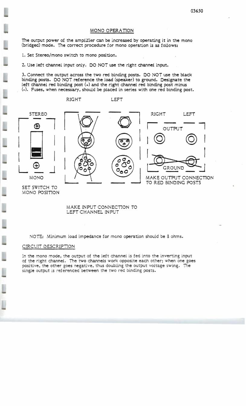
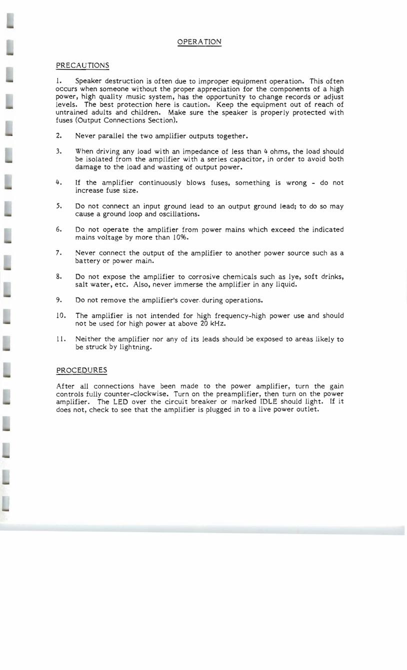
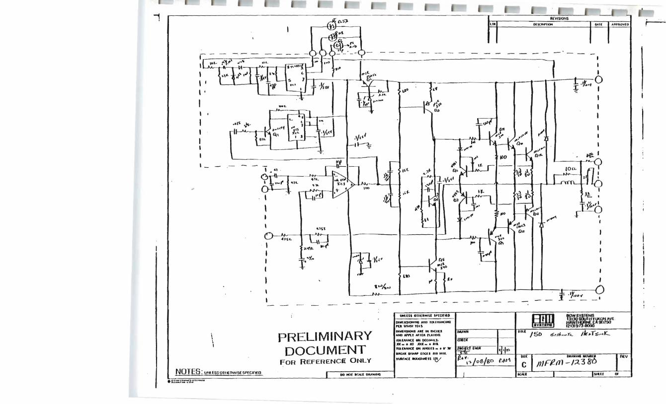
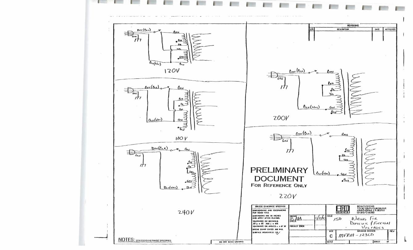
I
t-c~
6U (IV )
-ZOV
~
0 6dI ltgt~t- 6coJ
7
Cgtv(w-)
I()O V
~1UJifJ
6ur
Bv(lJ-
-ztfOV
NOTES ur ES501~nWISE SPEClflm 00 riOT SCN [ ~V1Ha
R[VISIONS
Ull O(SCIIIKlH DAl( AlPnOV(O
) baJ-~~ 0 sect~) ~
rh ~ 3 ~
-zoov
-=9 )ti6L1 - -~-----0 -shy - cshy
rt7
PRELIMINARY DOCUMENT
FOR REFERENCE ONLY
220V
UHll$S 01 H(RWIS[ snCIUfO
OIM(HSIONltfC AND 100VlNfCIHO r tSA$1 YIU
UMOtSIOH5 Nt( Iii IIfCti(S AtIO APPlt ATTU PlArtHO
rouflulaquol Off ()(CU-I Ja Ell t J)J JIXIl = 010
JOl(llHC( ON AHGlU a lD
IUA Slwtr (1)((5 bull 10 MAJ
IUlfAC[ ROtKOtipoundS5 Ie
tRofCI (Hajj
Ll
SIll
c SCA(
tUJ~ ISb
L-__ shy-r
~--- cshy -shy(~
~
2-_
IlGW~Y5EMS 13130 OUllt YlJI(ON AVE tiW tOt INECA 9025f1 12131913middot8000
L0lfl ~( Fc Dot-Egt Ie (rpoundE 1610-
Ico ( 116~ S OAAWIIKI NUItAMIII
- -lt3t()
SltUl l
BGW SYST~~S INC
ENG NO DESCRI~TlaN PART NO
PARTS iIST 150 ~ 12390
SCHEMATIC AC wIRIN~ MFR~ 12360 SCHEMAT[C CHASSIS MFRM l2370 SCHEMATIC HEATS[NK MFRM 12380 B~OCK ~IAGRAM MFRM 12390
A~L COMPONENTS _ITH DESIGNATIONS IN THE 200 SERIES ARE RIGHT CHANNEL HEATSINK NUMBERS - ~EFER Ta 100 SERIES NUMBERS EXAMPL~ 201 ~aULD BE THE SAME AS CIOl
CAPACITORS
1gt1 47 UF 2SV TANTALUM CI02 240PF SUOII MICA CI03 10PF 10011 MICA CI04 30 PF 50ull1 CA CI05 47UF 10V E~ECTR~~YTIC CLOt) 30PF SOu II ~ICA
Clgt7 12UF 10011 META~IlE) ~YLAR
(lO~ 12UF 10011 META~IlEJ MYLAR CI0 220PF 500 DISC C 1 1 ) lUF 2511 JISC ell 1 lOOOPF 50011 DISC (112 1000PF 5001 DISC C113 S60PF 5uOll MICA C 1 14shy 240PF 50011 MICA Cl15 l2uF 10011 ~ETA~IlEJ ~YLAR Cl15 12uF 10011 METALILEJ MYLAR Cl17 12UF 100V METAiIlEJ MYLAR Cl1 1UF 25 )I5C Cll~ bull 1 UF 2511 J I SC C12) 1UF 2511 JISC 121 015UF 10011 MYLAR C122 1UF 25 JISC (123 47uF 10011 META~ILEJ ~YLA~ C 12+ 1UF 2511 )IiC C125 430PF 100 IICA C12l tUF 2511 DISC C301 OlvF 50011 DISC C302 8500UF SOli E~ECTRQLtTIC
C3gt3 8500UF 501 ELECTqQLtTIC C304shy 01UF 25 JISC C3JS OluF 25V JISC
0226-0005 0090-0240 0060-0010 0060-0030 0456-0047 0060-0030 0363-9003 0363-8003 0100-0220 0129-0100 0100-1000 0100-1000 0080-0560 0090-0240 0363-8003 0363-8003 0363-8003 0129-0100 0129-0100 0129-0100 0369-0015 0129-0100 0363-3000 0129-0100 0060-0430 0129-0100 Ot99-0100 0533-IJOOd 0533-0008 0129-0100 0129-0100
ENG NO
=gt101 0102 )103 01 +
~1S 0100 ) 107 ~10j
~3Jl
rcia 1 IC1J2 r C 103
J 1 J 1
J301 J302 J3JJ J 3J 4
J305 J30~
J307 J30~
J30~
J310 J311
1 0 1
P3J1 PJOZ
JIJ1 0102 0103 01J4 (HOS
01)6 0107
12390-2
BGw SYSTEMS lNC
OESCRIPT[J~
DIODES PART 0
IN41461N914 OI~DE IN414d1N914 DIODe IN400~ DIJDE lA 400V IN4004 DIJDE lA 4QOV lN4740A IOV ZENER DIODE IN4740A IOV ZEN~R DIODE 1N414d1N914 DIODE IN41481N914 DI~Dc B~IDGE RECTFIE~ ~Brl2502
1900-4148 1900-4146 1900-4004shy1900-4004 1900-4740 1900-4740 1900-414d 1900-4148 1886-2502
INTEGRATED CIRCU[TS
LEVEL DETECTOR TI~ER ~~555
OP AMP NE5534
TL0467CP 1685-0487 18d5-0555 1685-5534
JACKS
MOLEX 12 ~IN CO~NECTOR 03-09-2121 INPuT JAClt Nlll r NPU r J A Clt Nil 1
6 PIN SQCtltET 6 PIN SOCKET 3 PIN XLR PC ~O~NT 3 PIN XLR ~C MOUNT STE~EO PH~NE JACK 39 BUSHING CJNNECTQR 3INDI~G POST RED CONNECTOR 3INDr~G POST RED CJNN~crOR 3IN~I~G POST BLACK CONNEcrOR 3INDI~G POST BLACK
1231-2121 9999-0111 9999-0111 1203-0006 1203-0008 1205-0002 1205-0002 1205-0005 1231-0008 1231-0008 1231-000~
1231-0009
I ~DUCTOR S
14JH INDUCTOR 22GA MIRE 8022-0400 SEE R128 1700-0001
PLUGS
MOLEX MOL~X
12 12
~IN ~O~NECTOR 03-09-1126 ~IN CO~NECTOR 03-09-1126
1231- 1 1 26 1231-1126
TRANSISTORS
2N2484 NPN SI~ICON LOW SIGNAL r09~
MJE lSO~8 rRANSISTOR NPN r0220 MJE 350 PNP r~ANSlsrOR
MJE J~O NP~ T~A~SISTOR
MJE 720 N~N rRA~SISTOR
2N4401 NPN 5r~ICON LO~ SIGNAL r092 2N4403 PNP SI~ICON LO~ SIGNAL rU92
1654-2484 1854-5028 1953-1) 350 1954-0340 l854-0720 l654-440 1 1853-4 03
123903
8G- SYSTEMS INC
ENG N) 01 Js 010~
0110 ) 1 1 1 ell 12 0113
Q10l ~lJ2
~ 1 J 3
RI04shy
U 15
RlelS ~107
HD~
~lel~
~110
~ 1 1 1 ~ 11 2 R113 en 1 4shy
~ 115 lt1 1 ~ R 11 7 ~11i
R 1 1
R12J ~ 1 2 1
~122
en 23 ~124-
~125
~12)
~127
~12j
~121
~13()
R131 ~132
R133 R134 R135 R13S R137 R138 R13~
R14J R 1 ~ I
Rl~2
DESCR1TI31 4JE 340 N)N THAlS 1 STO~ MJE 350 PNP TRAt4SISTOR MJ E 15028 NPN T~ANSISTOR T0220 MJE 15029 PNP TRANSISTOR T0220 MJ 15022 NPN TRANSISTOR T03 MJ 15023 ~P T~1SISTOR T03
RESISTORS
47K 5X 12~ DEPQSITED CAR~ON 475K IX ~ETA~ FI~M 475K 1~ ~ETA~ FI~M
~7K 5~ 12~ DEPOSITE~ CARBON 47K 5X 12w DEPOSITED CARBON 24~K 1~ META~ FI~M
100~ 5 12~ DEPOSITE3 CARBON 15K 5 12WDEPuS1TED CARBON 15K 5~ 12~ DEPOSITED CAR~ON 0~0~ 5 12w DEPOSITE3 CARBON odOR 5 12M DE~OSITEJ CARBON o~R 5 12~ DEP~SITED CARBON 1JOR 5 12~ DEQO~ITE3 CARBON FACTORY SE~ECTEJ aFFSET ADJUSTMENT 27~ 5 1211 0E~OSITED CARBUN 470R 5 12~ DEOSITE) CARBON FACTORV SE~ECTE3 alAS ADJUST~ENT 100R 5 12~ DE~OSITEJ CARBON 100R 5~ 12~ DE~OSITEJ CARBON 1~ 5 12M DEPOSITE3 CARBON 1~ 5 12 DEPOSITED CARBUN 100R 5 12 DEPOSITE) CARBON 100R 5 12 DEOSITEJ CARBON 27R 5 2 wIRE laquoOUlD BIIIH 27~ 5 2M MIRE OU~D 8~H
O 1~ 5 211 IRE wOUND BwH O 1 R 5 2M If I HE IOUND 8wH ~ () R lOX 2M CARB)N COMP SEE ~101 270R 10~ 2~ M 1 RE MOUND SIIIH 33R lOX 2M MI~E ~OUND BWH 820R 3~ WI~E WOJNO 27lt 5~ 12~ DE~OSITEJ CARBON 24K 5~ l2 DEPOSIT~D CARBON 47K 5 12~ DEPOSIT2D CAR80N 100lt 5~ 12 OEPO~ITEJ CA~80N 1~ 5 12~ DEPOSITED CARBON 820R 5~ 12w OEOSITE3 CARBUN 10K 5~ 12~ DEPQSIT~D CARSON 39~ 5~ 12A DE~OSITE) CARBON 100lt 5 12w DEPOSITED CARBUN 10K 5~ l~W DEPOSIT~D CARBON 3~lt 5X 12~ OE~osrTEJ CARBON
PART 40
1854-0340 1853-0350 1854-5028 1853-5029 1854-1522 1853-1523
5005-4703 5001-4752 5001-4752 5005-4702 5005-4702 5001-2491 5005-1002 5005-1503 5005-1503 5005-0801 500 5-6d 01 5005-0800 5005-1002
5005-2702 5005-4701
5005-1002 5005-1002 5005-1003 5005-1003 5005-lU02 5005-1002 4025-2070 4025-2070 4025-1009 4025-1009 6020-1001
4020-2701 4020-3300 4030-8201 5005-2702 5005-2403 5005-4703 5005-1005 5005-1006 5005-3201 5005-1004 5005-3902 5005-1005 5005-l004 5005-3902
12390-4
aG~ SYSTMS INC
NG NO DESCRlTION PART 140
~143 2JOR 5 12M DEOSITE) CARBON 5005-2002 R144 2aOR 5 12 DEOSITED CARBON 5005-2002 R145 82)( 5 14- DEPOSITEgt CAkSON 5065-8202 R14~ 82)( 5 14- ~EPOSITED CARSON 5065-8202 Q3Jl 22K ST~P ATTENUATOR NOSLE 7006-2015 R3J2 22K ST~P ATTENUATOR NOBLE 7006-2015 Q303 27lt 5 2 CARSQN CO~~P 6025-2702
S I TCHES
SlOl T1E~I4A_ SolITCH JOR 212F 0630-3445 53J1 5-IDE SITCH R~CESSEgt HANDLE 0620-1)206
TRiNSFORMERS
T3Jl 0900-0l24
TEiUH NAL 5T~ IPS
Ta30l G~OUND aA~QIER STRI ~STRA 0720-1696
____________ __
WARRANTY REGISTRATION PLEASE FILL OUT AND RETURN THIS CARD WITHIN 2 WEEKS FROM DATE OF PURCHASE
NAME DATE PURCHASED
ADDRESS PHONE
CITY STATE ZIP
PURCHASED FROM DEALER
ADDRESS
CITY STATE ZIP
MODEL NUMBER _________
SERIAL NUMBER _______shy
PURCHASE PRICE ________
FOR WHAT PURPOSE IS THE UNIT INTENDED
HOME STUDIO SOUND REINFORCEMENT OTHER (EXPLAIN)
IS THIS AMPLIFIER A REPLACEMENT FOR AN EXISTING UNIT
I F YES) WHAT KIND ___________________
WHY DID YOU CHOOSE A BGW POWER AMPLIFIER
__DEALER RECOMMENDAT ION _~MAGAZINE ADVERTISEMENT
__SOUND QUAL ITY __TECHNICAL DESIGN
~_OTHER __FRIENDI S RECOMMENDATION
COMMENTS
SYSTEMS middot
13130 SOUTH YUKON AVENUE ~AWTHORNE CALI FORN LA 90250
------~--------------------- ----------_ _------------------------------shyFOLD HERE
----------------
---
SERVICE AtmiORIZATION FORM
PLEASE COMPLETE THIS FORM AS COMPLETELY AS POSSIBLE AlID RETURN TO BGW SYSTEMS BEFORE RETURNING UNIT
NAL1E ---------------- PHONE
ADDRESS (CITY) (STATE) (ZIP)
UNIT -----------------------------------MODEl SERIAL NUMBER
1 DESCRIBE SYMPTOMS
2 bull WHI CH CHANNElS (S ) EXHIB ITS THE PROBlEMS
3 WHAT OTHER EQUIPMENT WAS INVOLVED
MANUFACTURER MODEL NO PREAMP SPEAKERS
4 UNDER 1NHAT CONDITIONS DOES THE PROBLEM OCCUR (CHECK THOSE THAT APPLY)
A ALL THE TL1E ____ B AFTER AWHILE C AT HIGH VOLUME=-LE~VE=L--S-D AT HIGH TEMPERATURES ______ E OTHER (EXPLAIN)
5 HOW OFTEN DID THE PROBLEM OCCUR
6 WHAT DID YOU DO TO ISOLATE THE PROBLEM TO TIlE POwER AMP
7 FURTHER COMMEITS
IT IS MORE ETIEDlUiT TO CALL YOUR DEALER OR OUR FACTORY EXPLAINING THE NATURE OF YOUR PROBLEM IN MAllY INSTANCES THE PROBLEM Campl BE SOLVED WITHOUT RETURNING THE UNIT TO THE FACTORY WARNING TIlE UNIT MUST BE RETURNED IN AN ORIGINAL FACTORY CONTAINER IF YOU DO NOT HAVE ONE WE WILL PROVIDE A REPLACEMENT FOR $1400 FACTORY AUTHORIZED WARRANTY REPAIR STATIONS ARE LOCATED THROUGHOUT THE US CALL YOUR DEALER OR THE FACTORY FOR THE LOCATION OF TIlE SERVICE STATION NEAREST YOU
l3l30 SOUTH YUKON AVENUE
rtAWTHORNEI CALIFQIRrI IA 90250
bull FOUl HERE
middot r POLARI-T-Y --~-- _ v( b INSERTION LOSS
FREQUENCY RESPONSE ~
I shy
-~ --____
CJ lmiddotE ~ shy
I
20 - 20K RESPONSEI 1 shy((i I 600 OHM DRIVER1~syUJJJ 0900-9250 i 1TESTED I3Y 15K NOM LOAD
BRIDGING TRANSFORMER li ~ [ OdB REf15K - 15K V
o
dB 5
10
1000 3 4 5 6 7 B 91~ 2
20000
FREQUENCY IN CYCLES PER SECOND I
----
~ SYSTEMS 50001
------------------------ -- --shy13130 SOUTH YUKON A V ENUE HAWTHORNE CALIFOR N I A 90250
PHONE (213) 9 73-8090 TELE X NO 66- 4 -1 9 4
t-
MODEL 150 TEST EPORT
DA TE_ 1 9l--__1 _ t L C_f1_-__ ~ _ TECHNICIAN C- a 1 (r SERIAL NO_=-_ -- ( l 6_l~---J=--__ _O
LINE VOLT AGE _ __ -=L=---()-_V___
CH 1 CH2 MONO
Power at Clip (0 1 THO) 2- I -V 2 1 r J 7 ( 4- V8 ohms - vol ts out
6W kJ t l)WPower
Power at Clip (015 THO) I R- 4- J4 ohms - volts out PI J ~ 4 W JgtJ 0Power
THO 50 Watts - 8 ohms (20 1 Volts)
06 (20Hz 20kHz 611
Small Signal Bandw idth 8 ohms
- 3dB Freque ncy kHz f1 kHz
Noise Leve l Out put Noise Volt age
mV I 0 1 mV20Hz t o 20kHz
Quiescent Power 4- () Watts
10 5 83
5004-5
BGW Systems - Q A Check List
MODEL If SERIAL NO INSPECTORSIGNA TURE CHECK
15tJ J606
1- Front Panelchassis free of blemishes ~ 2 Knobs correctly aligned and tightened ~ 3 All controls and switches function normally
4- Check for stripped screw heads ~ 5 Correct voltage tag
6 Five-way binding posts tightened and correctly aligned ~ 7 Input jacks wired correctly and tightened ~ 8 Check for correct circuit breaker ~ 9 Check wire harness for neatness and pinched wires ~
lO Check for loose hardware ~
090l83
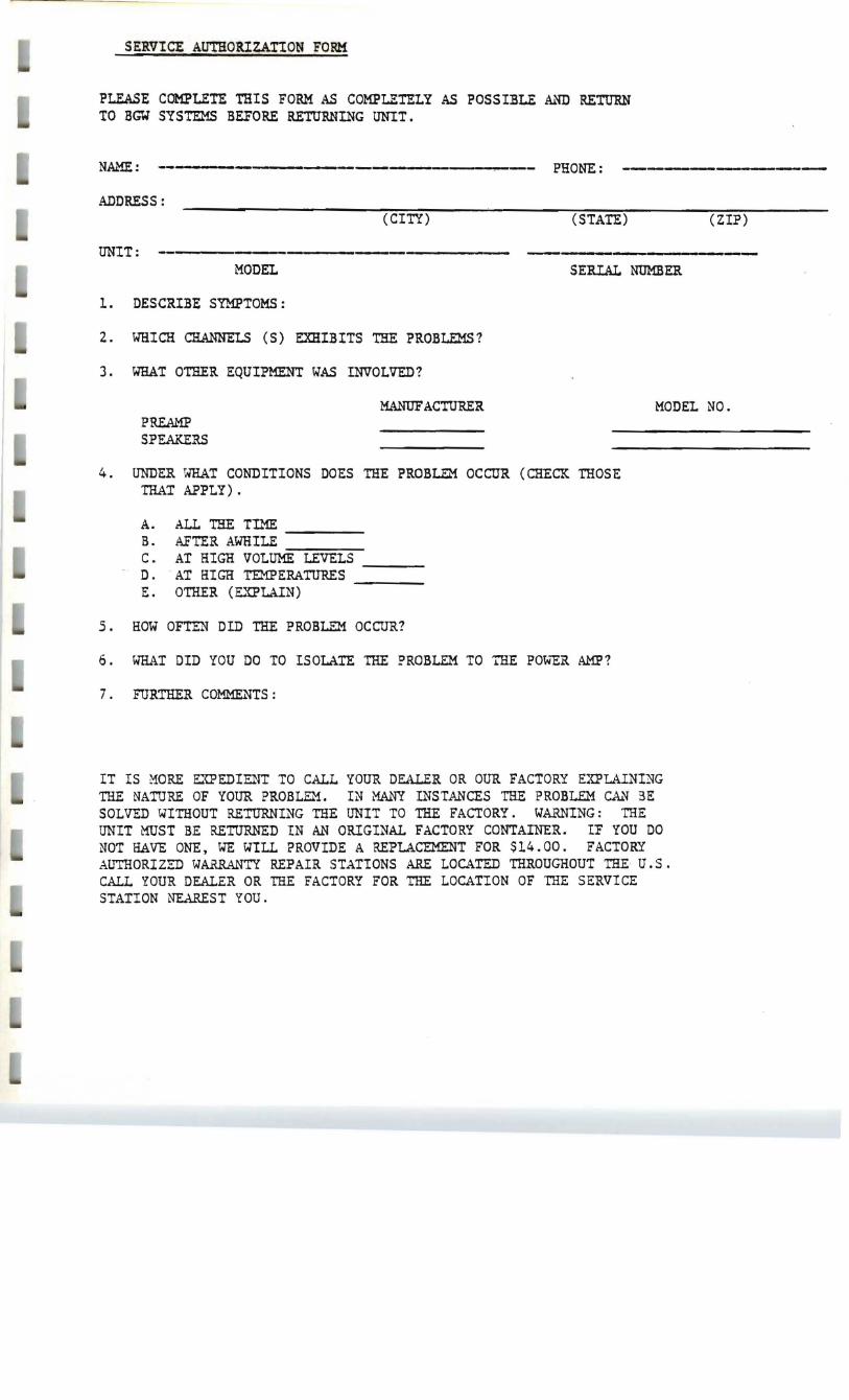
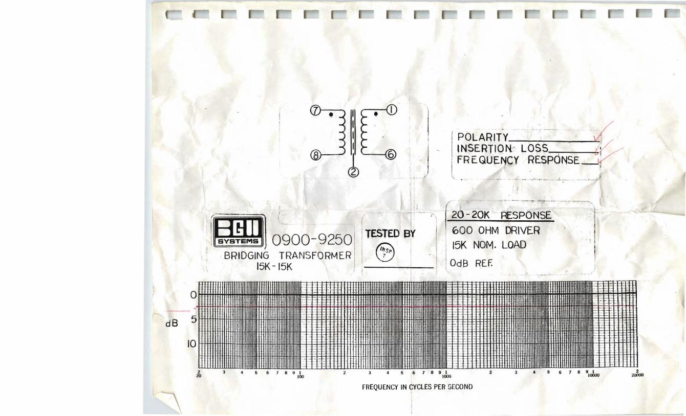
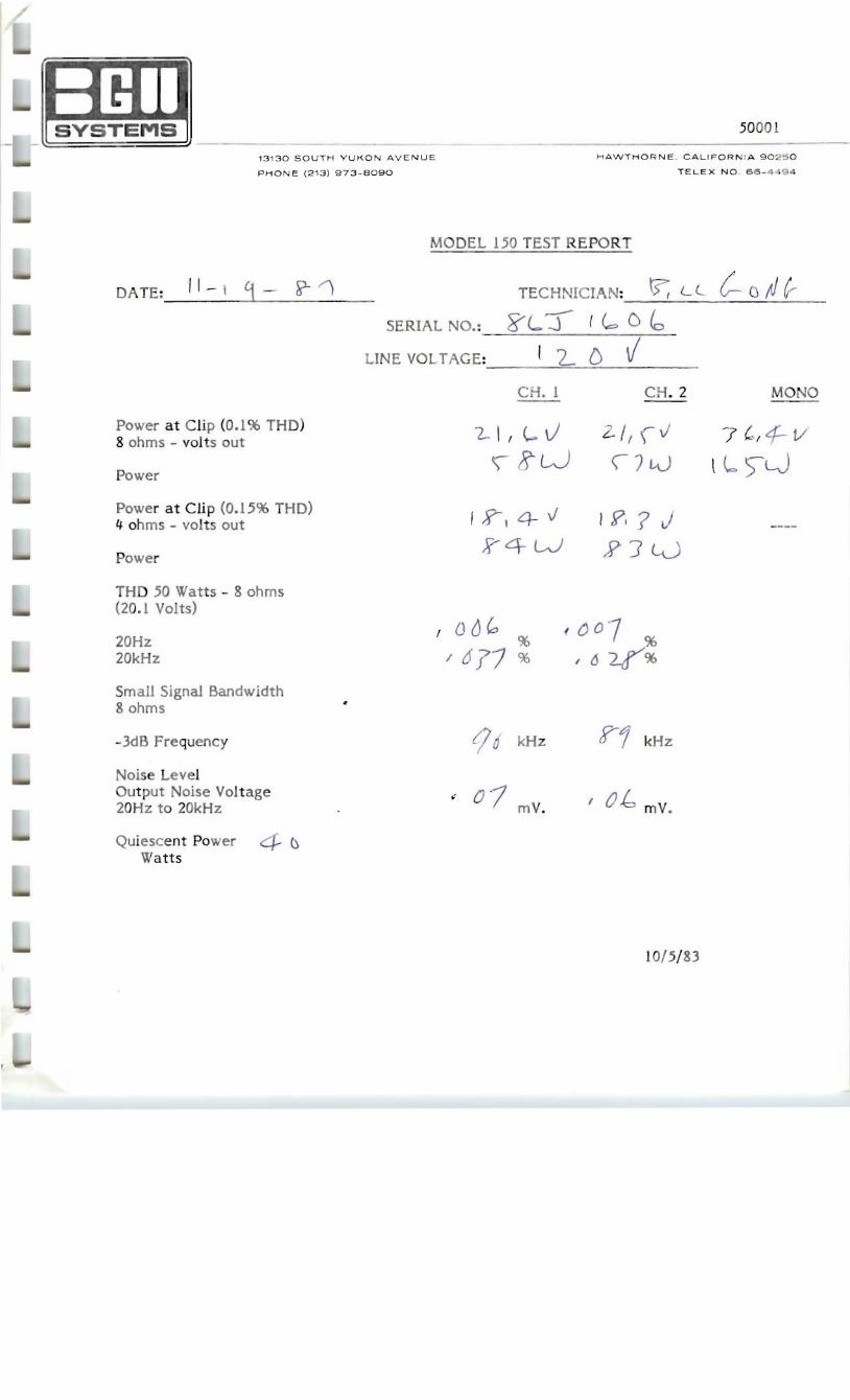
Recommended