1
Chapter 4.5. High Frequency Passive DevicesChapter 4.5. High Frequency Passive Devices

2
OutlineOutline
Inductors
Transmission lines
Varactors
MIM Capacitors
Resistors

3
Types of integrated inductors Types of integrated inductors (Yoon, RFIC-2003)(Yoon, RFIC-2003)
Stacked Helical Stacked MEMS
In silicon ICs:
●Spiral
●Multi-layer shunted
●Symmetrical spiral
●Stacked helical
4
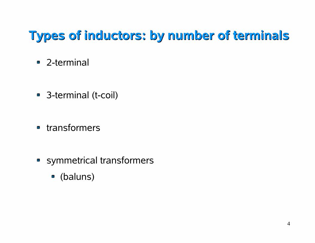
Types of inductors: by number of terminalsTypes of inductors: by number of terminals
2-terminal
3-terminal (t-coil)
transformers
symmetrical transformers
(baluns)

5
Inductor integration issuesInductor integration issues
Low quality factor (Q)
Large chip area (high cost)
Limited application frequency range:
lower bound limited by size and Q
upper bound (SRF=Self-Resonant-Frequency)
limited by dielectric thickness
Cross-talk through silicon substrate
GOAL is to AIM HIGH: high Q and high SRF
6
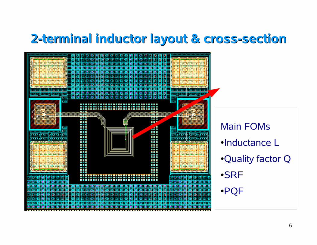
2-terminal inductor layout & cross-section2-terminal inductor layout & cross-section
Main FOMs
●Inductance L
●Quality factor Q
●SRF
●PQF

7
Inductance LInductance L
Inductance: induces and stores magnetic field
Greenhouse Equation
Lj1
Lj4Lj2
Lj3
Li1
Li3
Mij
L=total flux current
L=Self Inductance ∑i=1
n
Li + Mutual Inductance ∑i=1
n
∑j=2 j≠i
n
M ij
M>0 M=0M>0 M<0

8
Inductor QInductor Q
Q describes energy efficiency:
Conventional definition:
Q=stored energydissipated energy
Qeff=ℑ−Y11
ℜY11
PQF SRF
recommended range

9
0.13 0.13 µµm CMOS two-terminal inductor meas.m CMOS two-terminal inductor meas.
Leff=ℑ[Y11
−1]
Qeff=
ℑ[−Y11]
ℜ[Y11]

10
Loss mechanisms in inductors Loss mechanisms in inductors ((Dubuc et al, IMS2002Dubuc et al, IMS2002))
loss in metal
loss in substrate

11
Metal loss: series resistance RsMetal loss: series resistance Rs
DC-loss due to thin metal
and planar geometry
Frequency-dependent
cross-section due to skin
effect (B induced by
conductor itself)
Non-uniform current density
due to proximity effect (B
induced by neighbours)
J=JpJe where
∇×Jp=0; ∇×Je= jB; ∇ Je=0
Jp = potential current
Je = eddy current

12
Metal loss: techniques to reduce itMetal loss: techniques to reduce it
Multiple metal layers shunted (reduces PQF and SRF)
Thicker metal (needs process change)
More conductive metal i.e. Cu instead of AlCu (needs
process change)
Use narrower inner turns to reduce eddy current loss and
wider outer turns to reduce DC resistance (increases PQF
and SRF)
13
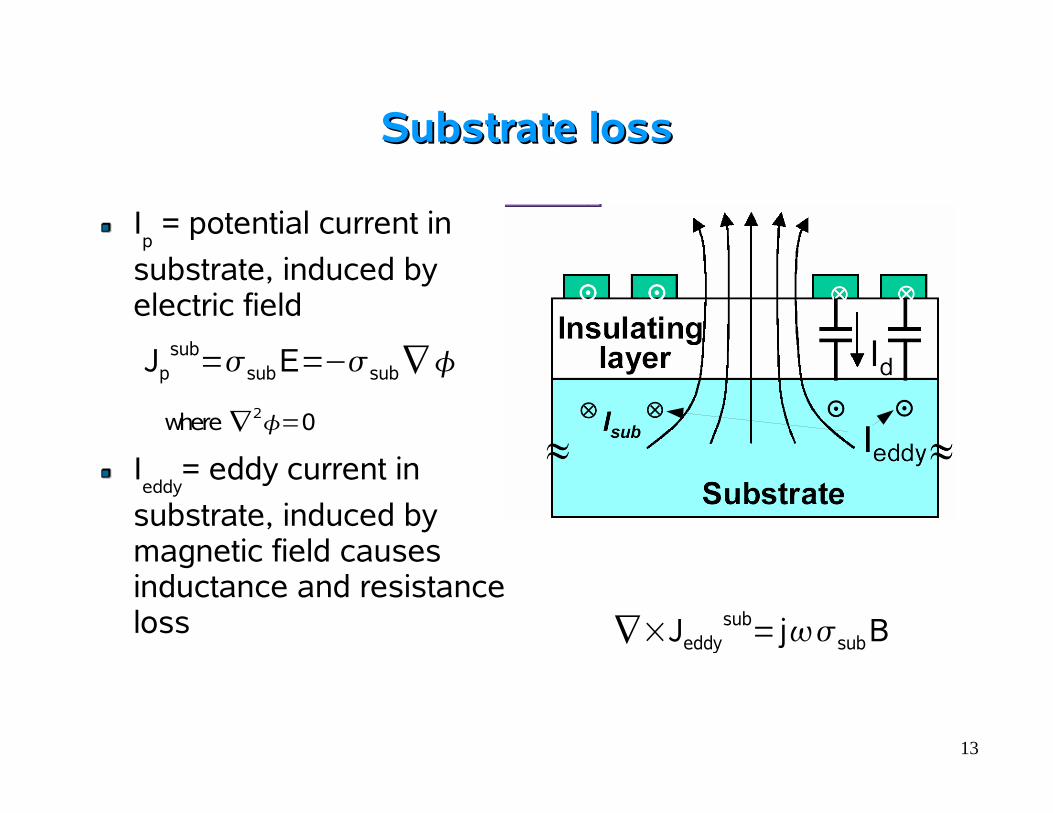
Substrate lossSubstrate loss
Ip = potential current in
substrate, induced by electric field
Ieddy
= eddy current in
substrate, induced by magnetic field causes inductance and resistance loss
Jpsub=subE=−sub∇
where ∇ 2=0
∇×Jeddysub= jsubB
14
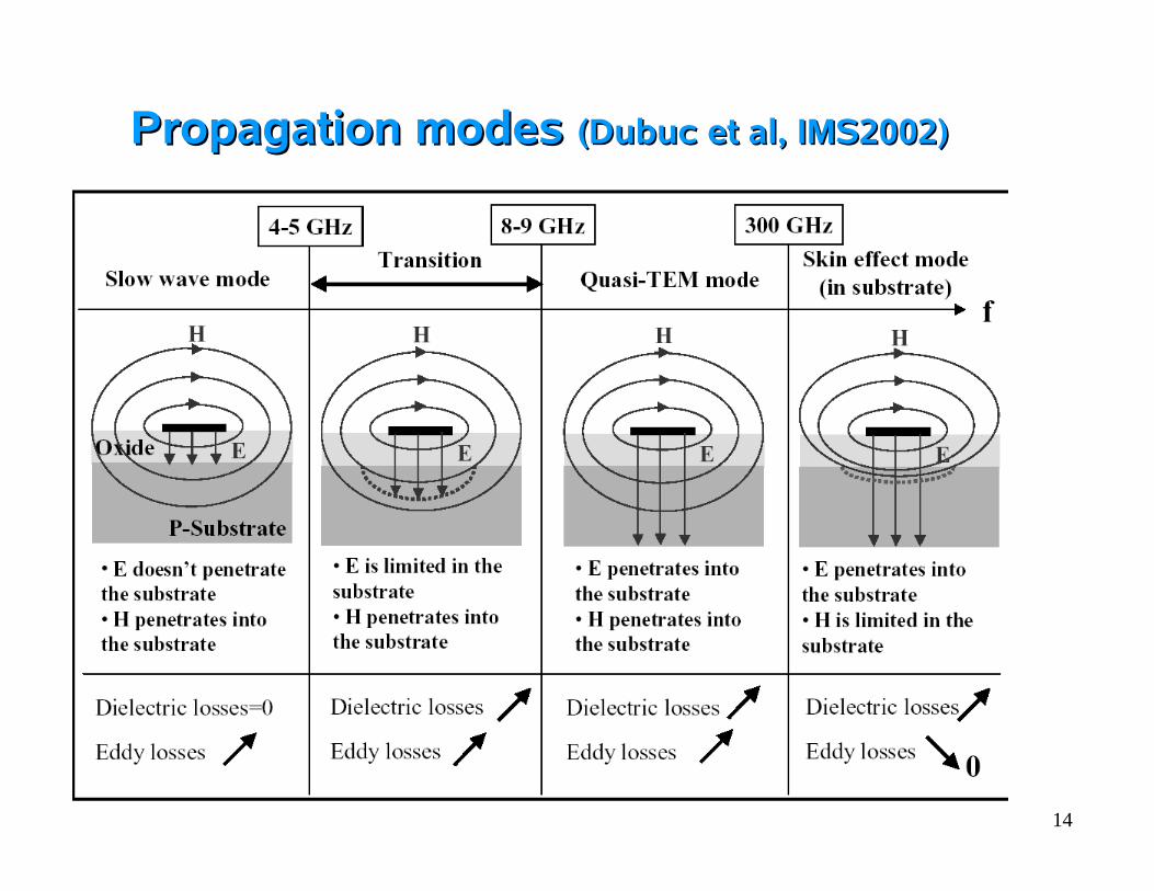
Propagation modes Propagation modes (Dubuc et al, IMS2002)(Dubuc et al, IMS2002)

15
Substrate loss: techniques to reduce itSubstrate loss: techniques to reduce it
Minimize electric coupling to substrate (Id) (also increases
SRF and PQF):
small inductor area
increase dielectric thickness (process change ?)
low-k dielectric (process change)
Reduce eddy currents in substrate
pattern shield (reduces PQF, SRF)
Reduce both eddy and potential currents in sub.
increase substrate ( =>0) (process change)
Place sub contacts 30 m .. 50 m from inductor

16
HF inductor equivalent circuits: simple HF inductor equivalent circuits: simple
W ST
P

17
Equivalent circuit model equations: simple Equivalent circuit model equations: simple Cao Y. et al., JSSC March 2003
L (see t-line-over-substrate equations)
n = number of turns
d = outer diameter of inductor
davg
= arithmetic mean of inner and outer diameter
0 = 4 10-13 H/m is the permeability of vacuum
Rs has DC and AC (frequency dependent) terms
s is the conductivity of the metal
RDC= l
W t
RAC= l
W 1−exp −t = 1
f
L≈60n2davg
2
11d−7davg
18
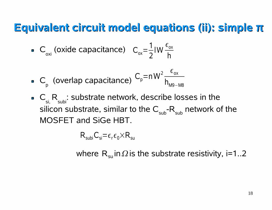
Equivalent circuit model equations (ii): simple Equivalent circuit model equations (ii): simple ππ
Coxi
(oxide capacitance)
Cp (overlap capacitance)
Csi,
Rsubi
: substrate network, describe losses in the
silicon substrate, similar to the Csub
-Rsub
network of the MOSFET and SiGe HBT.
Cox=12
lWox
h
Cp=nW2 ox
hM9−M8
RsubiCsi=r0×Rsu
where Rsu in is the substrate resistivity, i=1..2

19
HF inductor equivalent circuit: 2-HF inductor equivalent circuit: 2-ππ

20
Parameter extraction (2-terminal Parameter extraction (2-terminal circuit) circuit)
L=ℑ[−Y12
−1]
R=ℜ[−Y12
−1]
Rsub1=ℜ[Y11Y12−1]
●At low frequency (0.5 GHz to 1 GHz) extract directly:
Rsub2=ℜ[Y22Y12−1]
COX1=[−ℑ[Y11Y12
−1]]−1
COX2=
[−ℑ[Y22Y12−1]]−1
Csi=r0×Rsu
Rsubi

21
Parameter extraction (2-terminal Parameter extraction (2-terminal circuit)circuit)
●At high frequency (5 GHz to beyond SRF) :
calculate (and/or optimize):
CP from imag(Y
12),
skin effect parameters Lf, R
f from real(Y
12),
Csubi
from imag (Yii+Y
12)

Scaling of inductors to mm-wave frequencies Scaling of inductors to mm-wave frequencies Scale size and frequency: f->f×S, W->W/S, l->l/S, d->d/S, h-
>h/S, t=ct.
Small footprint to minimize loss in silicon
L≈60n2davg
2
11d−7davg
LS≈
60n2[ davg
S ]2
11dS−7
davg
S
Cox=12
lWox
h
Cox
S=
12
lS
WS
ox
hS
Cp=nW2 ox
hM9−M8
Cp
S=n W
S 2
ox
hM9−M8
SSRF≈
12L COXCp
S×SRF=1
2 LSCOX
S
Cp
S

Scaling of inductors to mm-wave frequencies Scaling of inductors to mm-wave frequencies
Vertical stacking and magnetic coupling to
Increase inductance/area
reduce loss in substrate
Outcome
Inductors/transformers can be as small and inexpensive as
transistors
As in MOSFETs, series resistance does not scale
Q remains the same, but at fS
RDC= l
W t RDC=
lS
WS
t
RAC=
lS
WS1−exp−t

Slide 24
140 pH Planar Spiral Inductor in 90-nm CMOS140 pH Planar Spiral Inductor in 90-nm CMOS
d = 29 m, n = 2.25S = 2 m, W = 2 µm
t = 3 m Measured vs. ASITIC simulated Leff
and Q
eff

25
3-terminal inductor layout3-terminal inductor layout

26
3-terminal inductor equivalent circuit3-terminal inductor equivalent circuit
P1 P2
P3
k
L11 R11 L22 R22
2xRs1 Cs1/2 2xRs2 Cs2/22 Rs1×Rs2Rs1Rs2
COX12
COX22
Lt
Rt
COX1COX22
C s1C s22
CP

27
Model parameter extractionModel parameter extraction
L11=ℑ[Z11]
R11=ℜ[Z11]L22=
ℑ[Z22 ]
R22=ℜ[Z22]
M=−ℑ[Z12 ]
=−ℑ[Z21]
Rt=ℜ[Z12]=ℜ[Z21]
Ldiff=ℑ[Z11Z22−Z12−Z21]
Qdiff=
ℑ[Z11Z22−Z12−Z21]
ℜ[Z11Z22−Z12−Z21]
k=M
L11× L22
Coxi
, Rsubi
, Csi are extracted from the 2-terminal equivalent.

28
Single-ended vs. diff.-mode inductanceSingle-ended vs. diff.-mode inductance
Ldiff=L11L222M=2.2nH
Lsingle=L11=L22=0.67nH
●Strong mismatch can occur in either differential mode
or single-ended/common-mode if tight coupling in 3-term
inductors exists.
●Use 3-terminal inductors only inside the chip, not in
output buffer.
●Watch out for sign of M! Ldiff
should be larger than 2L11
.

29
HF inductor layout designHF inductor layout design
High SRF: narrow metal, wide spacing, minimum diameter
High Q : wide, thick metal, shunted metal layers
Large L/ area and SRF: large diameter, narrow metal,
stacked, series-connected metal layers
Substrate p-taps in 25-50 µm proximity
Minimize size in differential ckts.: use one center-tapped
differential inductor, rather than two inductors (but lower
overall SRF)

30
High Q & high SRF inductor design tipsHigh Q & high SRF inductor design tips
Small diameter
Narrow (narrower in inner turns), (W)
thick, (T)
widely spaced (S)
top metal -only (stacked structure for peaking inductors)
windings on
thick dielectric (h)
with low permittivity (OX
)
31
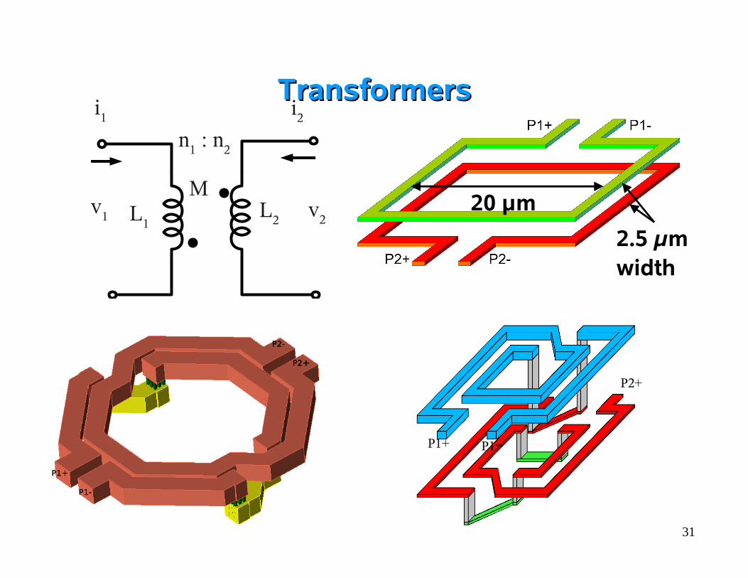
TransformersTransformers
P1+ P1-
P2+
L2 L
1
n1 : n
2
v1 v
2
i1
i2
M20 µm
2.5 µmwidth

32
3-D stacked transformer modelling3-D stacked transformer modelling
20 µm
2.5 µmwidth
ASITIC modeling procedure1. Use “pix” on bottom coil
alone to find COX, CSUB, RSUB, R2, L2
2. Calculate CSUB
3. Use “pix” on top coil alone to find R1 and L1
4. Use “pix” on top coil with bottom coil grounded to get C12
5. Use “k” command on both coils together to find coupling.

1:1 vertically stacked transformer in 90-nm CMOS
n=2, W= 2µm, S=2µm, t=3µm
Transformers in SiGe BiCMOS and 90nm CMOSTransformers in SiGe BiCMOS and 90nm CMOS1:1 vertically stacked SiGe BiCMOS transformer
n=2, t=3µm
34 µm

Baluns (symmetrical transformers)Baluns (symmetrical transformers)
P1+
P2+ P2-
P1-
k k
COX11 COX12 COX13
COX21 COX22 COX23
LP/2 RP/2 LP/2 RP/2
LS/2 RS/2 LS/2 RS/2C11 C22 C33
RS21 CS21 RS22 CS22 RS23 CS23
RS11 CS11 RS12 CS12 RS13 CS13

35
OutlineOutline
Inductors
Transmission lines
Varactors
MIM Capacitors
Resistors
36
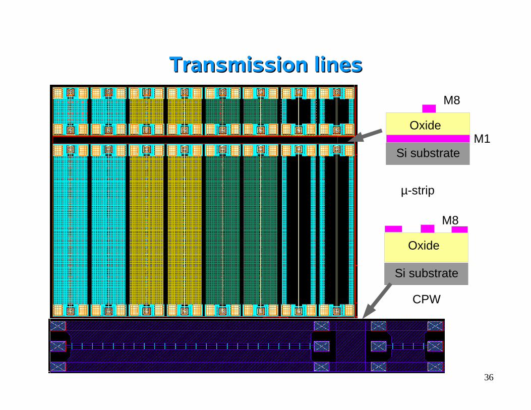
Transmission linesTransmission lines
Oxide
Si substrate
M8
M1
Oxide
Si substrate
M8
µ-strip
CPW
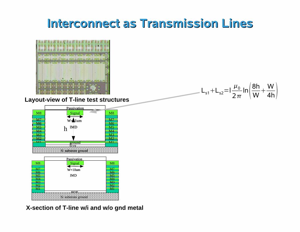
Interconnect as Transmission LinesInterconnect as Transmission Lines
FOXSi substrate ground
SignalM8
M7M6M5M4M3M2M1
M8
M7M6M5M4M3M2M1
W=10um
Passivation
IMD
FOXSi substrate ground
SignalM8
M7M6M5M4M3M2M1
M8
M7M6M5M4M3M2M1
M8
M7M6M5M4M3M2M1
M8
M7M6M5M4M3M2M1
W=10um
Passivation
IMD
ground
SignalM8
M7M6M5M4M3M2M1
M8
M7M6M5M4M3M2M1
W=11um
Passivation
IMD
ground
SignalM8
M7M6M5M4M3M2M1
M8
M7M6M5M4M3M2M1
M8
M7M6M5M4M3M2M1
M8
M7M6M5M4M3M2M1
W=11um
Passivation
IMD
FOXSi substrate groundSi substrate ground
X-section of T-line w/i and w/o gnd metal
Layout-view of T-line test structures
Ls1Ls2=l0
2ln8h
W
W4h
h

38
Transmission linesTransmission lines
Show up in ICs:
by design: as circuit matching elements (preferably as
Metal-Oxide-Metal – MOM lines), or
inevitably, as interconnect (as Metal-Oxide-Silicon lines)
In Si ICs, -strip or GCPW have lower loss than CPW
Use M1, M2 or M1+M2, M1+M2+M3 ground planes
Loss mechanisms similar to inductors (no proximity effect)

39
Transmission line params and modelsTransmission line params and models
Most important HF performance parameters:
Characteristic impedance: Z0
Attenuation (/mm):
Group delay (/mm):
Use simulator built-in models for GaAs, InP, Si M-O-M strip
lines (ADS > Hspice > Spectre)
Use lumped scalable RLC model for Metal-Over-Silicon lines
Can be extracted from measurements or EM simulations

40
T-line de-embedding technique T-line de-embedding technique Goal: Remove impact of pad parasitics
Test structures: long (1.2/0.6 mm) and short (200/100
µm) lines
How? 1-step de-embedding based on ABCD and Y
matrices
Outcome: Determine ZC, γ, α, τ
G, ε
eff of intrinsic line
from ABCD matrix.
41
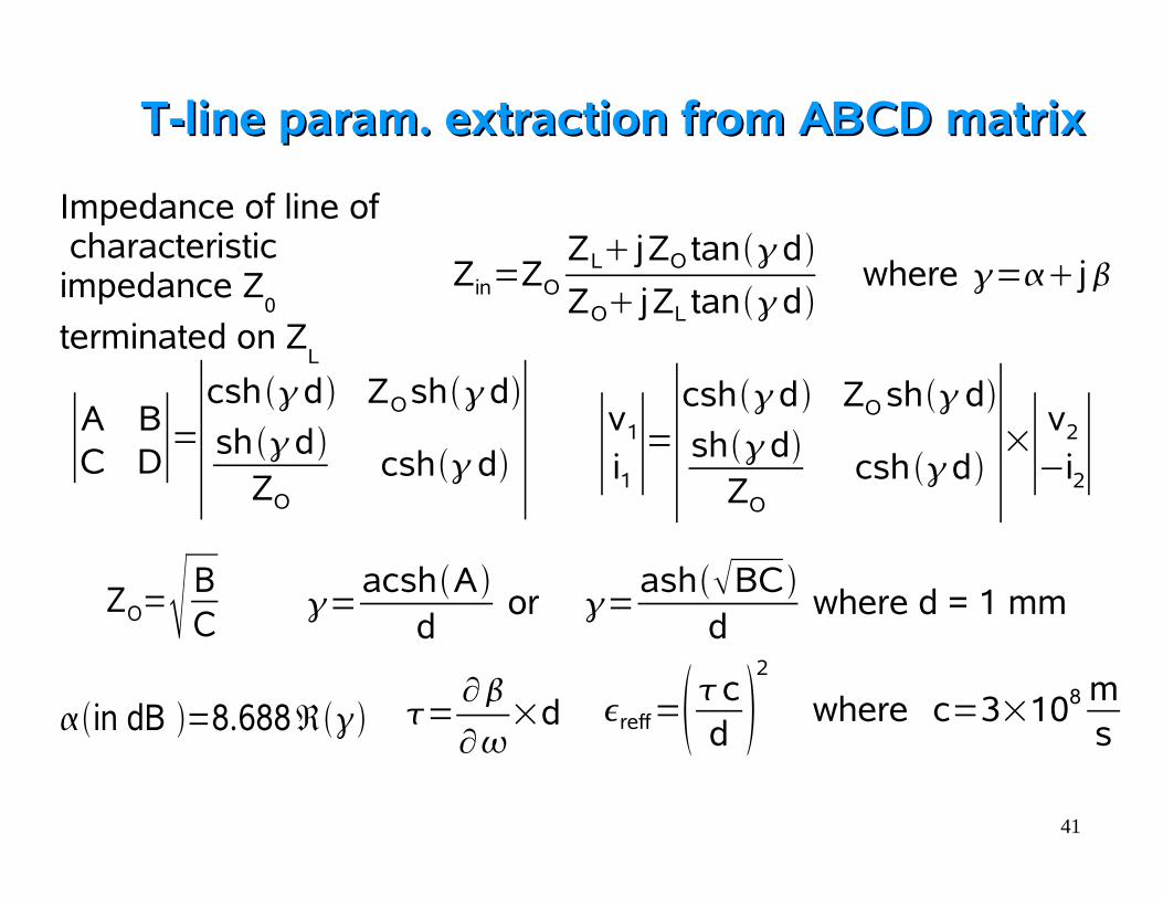
T-line param. extraction from ABCD matrixT-line param. extraction from ABCD matrix
Zin=ZO
ZL jZO tand
ZO jZL tand where = j
∣v1
i1∣=∣cshd ZO shd
shdZO
csh d ∣×∣ v2
−i2∣
=acshA
d or =
ashBC
d where d = 1 mm
∣A BC D∣=∣
csh d ZOshd
sh dZO
cshd ∣ZO= B
C
in dB =8.688ℜ =∂
∂×d reff=c
d 2
where c=3×10⁸ ms
Impedance of line of characteristic impedance Z
0
terminated on ZL

Simple lumped ckt. model without skin effectSimple lumped ckt. model without skin effect
P1 P2
L/2 R/2 L/2 R/2
Cs
COX
Rs
P1 P2
L/2 R/2 L/2 R/2
CdGd
P1 P2Z
1Z
1
Z2
Oxide Passivation
Signal line
GND
CB=
C
L ( ) 21
2
cosh1
−≈−
Aω
LC

Extracting the lumped circuit parametersExtracting the lumped circuit parameters
Simulate (in HFSS) a line with l>=10m to find ABCD params.
Find L/C and LC (high freq.)
G may be considered negligible
Optimize Lf,R
f, & R
m (skin) to fit & of model to HFSS simulation
or measurements
Compare simulations of 100m or longer lines to verify scalability

Example: Modelled vs. mea. 3.6-mm Example: Modelled vs. mea. 3.6-mm µµstrip linestrip line
Fitted RLGC model

Comparable SiGe vs. CMOS Comparable SiGe vs. CMOS µµstrip linesstrip lines
CMOS-line attenuation getting slightly worse in new nodes
0.4 dB/mm @50GHz, 0.5 dB/mm@ 65GHz, 0.66 dB/mm@ 94GHz,
3.6mm long

46
T-line loss in thin and thick metal BEOLsT-line loss in thin and thick metal BEOLs

47
OutlineOutline
Inductors
Transmission lines
Varactors
MIM Capacitors
Resistors

Variable capacitance devices: VaractorsVariable capacitance devices: Varactors
Figures of merit
capacitance ratio:
CMAX
/CMIN
quality factor Q
linearity
Applications
VCO
Implementation
p-n junction
accumulation-mode MOS
capacitor

Common-sense rulesCommon-sense rules
Accumulation-mode MOS (AMOS) varactors have higher Q and larger tuning range than pn junction varactors
If varactor model is not available, build a rudimentary model:
use MOSFET with S/D tied together
Add gate resistance externally, as for MOSFET
Calculate CMAX
= COX
×W×L + 2Cov
CMIN
= CMAX
/2
Smaller varactors (W and Wf) have higher Q's at a given
frequency

50
Extraction of simplified equivalent circuitExtraction of simplified equivalent circuit
Cvar=[ℑ[−Y12
−1]]−1
Rsub=ℜZ21
Cnw=[ℑZ21]
−1
R=RGRCH=ℜZ11Z22−Z12−Z21
STI STI
n-well
gate
STI
p- substrate
n+ n+ p+
p-well

51
Meas. vs. sim. CMeas. vs. sim. Cvarvar(V) for 1.2V, 130nm device(V) for 1.2V, 130nm device

90nm AMOS varactors: C90nm AMOS varactors: Ceffeff
Scales well with Wf and L.
Physical model matches measurements of Ceff
well:
Captures dependence on Wf and L.
Captures bias dependence.
10x2µm L=0.25µm
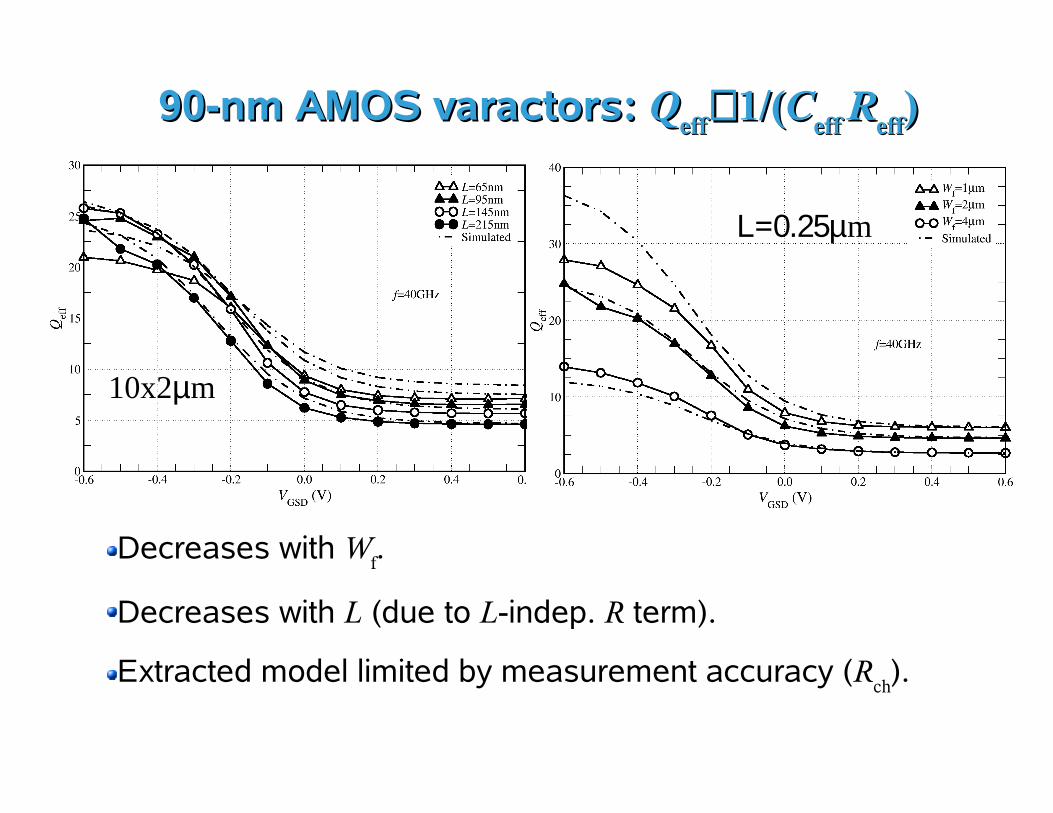
90-nm AMOS varactors: 90-nm AMOS varactors: QQeffeff∝∝1/(1/(CCeff eff RReffeff))
Decreases with Wf.
Decreases with L (due to L-indep. R term).
Extracted model limited by measurement accuracy (Rch).
10x2µm
L=0.25µm

Meas. 65-nm GP AMOS varactor at 94 GHzMeas. 65-nm GP AMOS varactor at 94 GHz
• Ldrawn
=60nm, Wf=0.55μm, Wtotal=27.5μm, CVAR=1.53fF/μm
• C variation: 25fF – 42fF, Q: 6 – 8 at 94 GHz
Double-sided gate
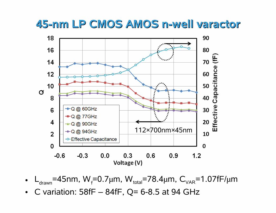
45-nm LP CMOS AMOS n-well varactor45-nm LP CMOS AMOS n-well varactor
112×700nm×45nm
• Ldrawn
=45nm, Wf=0.7μm, Wtotal=78.4μm, CVAR=1.07fF/μm
• C variation: 58fF – 84fF, Q= 6-8.5 at 94 GHz

MIM CapacitorMIM Capacitor
Figures of merit
Capacitance per area
Quality factor Q
Capacitance to
substrate
Issues with reliability
Very good linearity
Applications
VCOs
Low-noise amplifiers
mixers
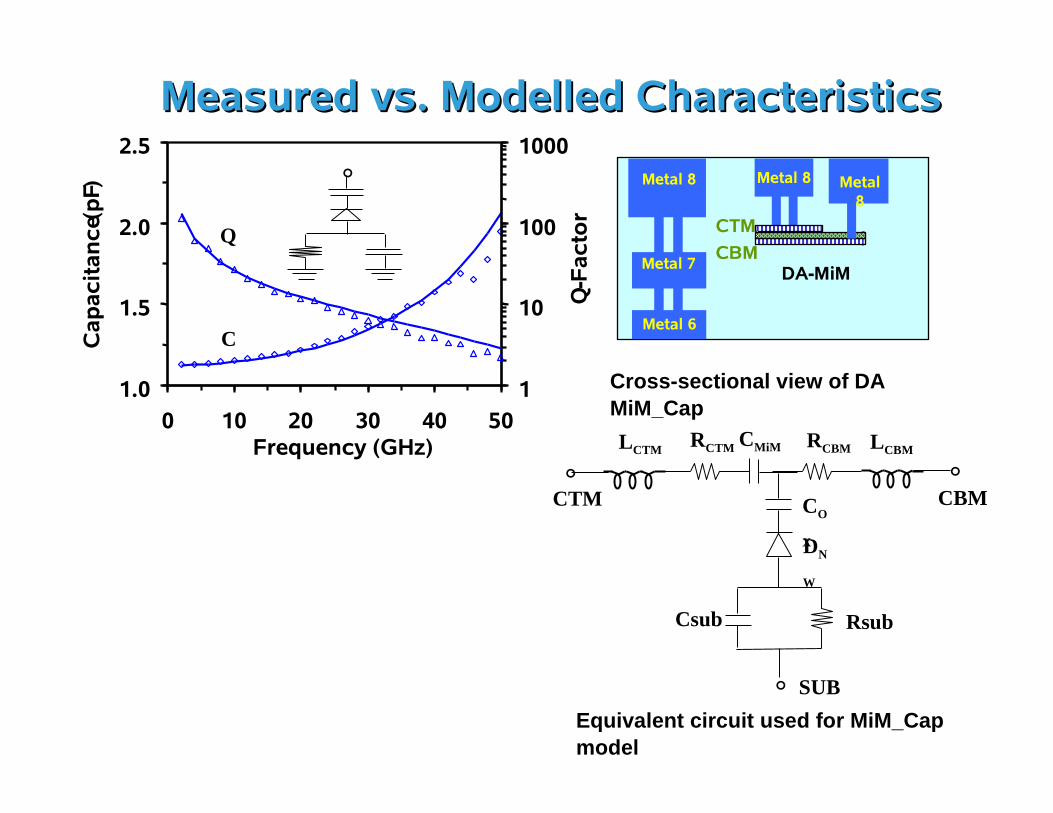
Measured vs. Modelled CharacteristicsMeasured vs. Modelled Characteristics
Cross-sectional view of DA MiM_Cap
DA-MiM
Metal 8 Metal 8 Metal 8
Metal 6
Metal 7 CBM
CTM
°
° °LCTM
SUB
CBMCTM
RCTM CMiM RCBM LCBM
CO
XDN
W
RsubCsub
Equivalent circuit used for MiM_Cap model
1.0
1.5
2.0
2.5
0 10 20 30 40 50Frequency (GHz)
Cap
acit
ance
(pF )
1
10
100
1000
Q-F
acto
r
1.0
1.5
2.0
2.5
0 10 20 30 40 50Frequency (GHz)
Cap
acit
ance
(pF )
1
10
100
1000
Q-F
acto
r
Q
C
°

58
HF MIM capacitor equiv. ckt. HF MIM capacitor equiv. ckt.
use reversed-biased n-well for good substrate isolation

MOM capacitorMOM capacitor
Uses the fringing capacitance between dense metals
Requires no additional process option (comes for “free”)
Lower Q than a MIM capacitor

60
Extraction of simplified ckt. for MIM/MOM capExtraction of simplified ckt. for MIM/MOM cap
Cmim=[ℑ[−Y12
−1] ]−1
Rsub=ℜZ21COX=[ℑZ21]
−1
R=RTOPRBO=ℜZ11Z22−Z12−Z21
CT CB
L R
Cs
COX
RsCT CB
Z1
Z2
C
CT CB
L R
Cs
COX
Rs
C

61
HF resistor equivalent circuit HF resistor equivalent circuit
STI
CoSi
W-plugRsheet
RCORCO
Rend Rend
T-circuit imposes use of Z parameters.
2-circuit is more accurate for long resistors but is in
most cases not necessary.

62
HF resistor equivalent circuit extractionHF resistor equivalent circuit extraction
L=ℑZ11Z22−Z12−Z21
R=ℜZ11Z22−Z12−Z21
Rsub=ℜZ21COX=[ℑZ21]
−1

63
RF padsRF pads
Top metal only
Reversed-biased salicided n-well or metal-1 grounded n-well

64
Using ASITIC to calculate HF equiv. ckt. Using ASITIC to calculate HF equiv. ckt. parasitic elements of passive components parasitic elements of passive components
MIM caps, poly resistors, varactors have identical substrate
network (Rsub
, Csub
)
Use ASITIC to −model the substrate network for a metal
line of similar width and length,
MIM caps and poly resistors are realized in the oxide, above the
silicon substrate
Use ASITIC to −model Cox
, L, R for a metal line of similar
width and length and located at the same distance from the
substrate as the MIM cap or poly resistor

SummarySummary
Inductors and transformers: main design components available to
HF circuit designers
Unlike transistors, they are almost insensitive to process variation
Inductors and transformers are scalable to at least 200 GHz
Modelling of passives as critical as the transistor model
In Si HF ICs t-line matching should be avoided < 100 GHz
because of large area
Varactors, capacitors and resistors have RLC parasitics which
must be accurately modelled at HF
Recommended