Degradation of ZnS:Cu,Au,Al phosphor powder and thin films under prolonged electron bombardment
by
Kenneth Thembela Hillie
(MSc)
A thesis submitted in fulfilment of the requirements for the degree
PHILOSOPHIAE DOCTOR
in the
Faculty of Natural and Agricultural Sciences
Department of Physics
at the
University of the Free State Republic of South Africa
Promoter: Prof. H.C. Swart Co-promoter: Prof. G.L.P. Berning
October 2001

Kenneth Thembela Hillie: PhD thesis
ii

Dedication
iii
This thesis is dedicated to the memory of the late
Prof. C.M. Demanet
as my mentor and later a valuable friend.

Kenneth Thembela Hillie: PhD thesis
iv
“For a successful technology, reality must take precedence over
public relations, for Nature cannot be fooled.” Richard P.
Feynman.

Acknowledgements
v
Acknowledgements: I am deeply indebted to the following people: • My wife Zou and son Mlibo for their constant support and understanding throughout
the duration of my research, I owe this to them. • Our parents, Ndzotho, Zola, Slush, Silos and the entire family for their support during
this period. • My promoter Prof. H.C. Swart for his professional leadership that made me grow as a
research scientist and for his wisdom. • Prof. G.L.P. Berning as being the former head of the department who allowed me to
embark on these studies and also as my co-promoter for his professional suggestions. • Prof. W.D. Roos for the informal discussions that made an impact. • J.K.O. Asante for always willing to listen and to the entire Physics department staff
who made the environment conducive. • Drs. C. Curren and C. Theron of the NAC for their valuable input for thin film
deposition and RBS analysis, respectively, and the assistantship I got from the NAC staff.
• Prof. S.S. Basson of the Chemistry department for the valuable discussions that we engaged on.
• Dr P.W.J. van Wyk of the electron microscopy unit UFS. • The Unitra physics department staff for granting permission to use their AFM. • The UFS Electronics and Instrumentation units staff for their prompt response when I
experienced a problem. Lastly, I would also like to extend my gratitude to the following organisations for financially sponsoring the entire project and myself. • National Research Foundation (NRF) • Deutscer Akademischer Austauschdienst/ DAAD scholarship (1998-2000) together
with the German embassy in Pretoria.

Abstract
vi
Abstract Auger electron spectroscopy (AES) and cathodoluminescence (CL), both excited by the same electron beam, were used to monitor changes in surface composition and luminous efficiency during electron bombardment. ZnS:Cu,Al,Au phosphor powders and thin films were subjected to prolonged electron beam bombardment of varying beam energies and different electron beam current densities in two different (O2 and CO2) vacuum gas ambients. The thin film phosphors were grown on Si (100) substrates by using XeCl (308nm) pulsed laser deposition (PLD) method. X-ray diffraction (XRD) measurements revealed that ZnS (100) films were preferentially grown on a Si (100) substrate. The RBS results show that the growth rate, increased with an increase of the N2 pressure in the deposition chamber during deposition. Degradation on both the powder and the thin film phosphors was manifested by a non-luminescent ZnO layer that formed on the surface of the phosphor according to the electron stimulated surface chemical reactions (ESSCR) mechanism. Lower current densities lead to a higher surface reaction rate, due to a lower local temperature beneath the beam, which resulted into a more severe CL degradation. A lower temperature beneath the electron beam may lead to an increase in the surface reaction rate due to the longer time spent by the adsorbed molecules on the surface, with a direct increase in the ESSCR probability. Low current densities would also lead to surface charging due to a lower electron conductivity of the phosphor resulting in an increase in the CL degradation rate due to band-bending. In the studies conducted between room temperature and 310 oC, an increase in the temperature led to a decrease in the surface reaction rate due to a decrease in the mean surface lifetime of the oxygen molecules on the surface, with a direct decrease in the ESSCR probability. Without the presence of the electron beam no chemical reactions, up to 310 oC, occurred on the surface. Therefore, local heating due to the electron beam irradiation is not responsible for the chemical reactions on the ZnS phosphor surface. At -125 °C the degradation was controlled by the residual small amount of water vapour in the system that is frozen at this low temperature. The thermoluminescence (TL) curves of the phosphor powder before and after degradation showed the influence of the O substitutional atoms that are created during electron bombardment in an O2 ambient. The O substitutional atoms acted as electron traps. On the electron beam bombardment of thin film phosphors, the degradation was more severe under O2 ambient compared to the same partial pressure of CO2 during electron beam bombardment, which is attributed to the free energy of formation of ZnO from ZnS when these respective gases are used. The degradation rate also depended on the energy of the electron beam, decreasing with increasing beam energy. This was interpreted according to the ionisation energy cross-section profile. The CL brightness increased

Abstract
vii
exponentially with the increasing energy beam as more free carriers that will subsequently recombine yielding CL, are excited at higher beam energies. The thin film phosphor was also subjected to the electron beam bombardment after the phosphor film was coated with a CdO film by using a chemical bath deposition (CBD) method. The surface reactions were electron beam stimulated, resulting in the desorption of both Cd and S from the surface which happened as soon as the surface adventitious C was depleted. Sulphur from the ZnS accumulated on the surface but was soon depleted as volatile SOx compounds. The CdO was reduced by an electron beam assisted mechanism in the presence of non-reducible ZnO in the CdO-ZnO system as the Zn from the underlying ZnS layer emerged to the surface. The CL intensity degradation of the coated film showed a dependence on the surface composition. The intensity remained constant until the Cd was reduced on the surface before a slight decrease was observed. The effect of the CdO capping layer on the intensity of the phosphor was evident until the CdO eventually disintegrated.
Keywords Phosphor: A wide band gap semiconductor that is intentionally doped with impurities to
emit the desired frequency of light.
Luminescence: It is a phenomenon whereby the emission of light occurs in excess of
thermal radiation.
Cathodoluminescence: Luminescence produced by electron beam irradiation.
Phosphor degradation: Reduction of the efficiency of a phosphor material through
prolonged electron bombardment.

Kenneth Thembela Hillie: PhD thesis
viii
Table of Contents
Title page ……………………………………………………………………………………… i
Dedication……………………………………………………………………………………… ii
Acknowledgement …………………………………………………………………………… iv
Abstract ………………………………………………………………………………………… v
Chapter 1 Introduction
1.1. Brief history of the display technology ……………………………..… 1
1.1.1. Cathode ray tubes (CRTs) ……………………………………... 1
1.1.2 Liquid crystal displays (LCDs) …………………………………. 2
1.1.3. Field emission displays (FEDs) ……………………………..… 3
1.2. ZnS phosphor degradation literature review ……………………….... 4
1.3. The aim of this study ………………………………………………….. 7
1.4. The layout of the thesis ……………………………………………..… 8
References ……………………………………………………………………. .. 9
Chapter 2 On the theory of luminescence processes of Zinc Sulphide (ZnS) based phosphor material
2.1. Introduction …………………………………………………………... 11
2.2. Energy transfer in the phosphors …………………………………..... 12
2.3. Quenching of luminescence ………………………………………..… 15
2.3.1. Action of adventitious impurities “killers”……………………. 15
2.3.2. Saturation…………………………………………………….……. 16
2.3.3. Concentration quenching………………………………….….…. 17
2.3.4. Thermal quenching………………………………………….……. 17
2.4. Decay characteristics ………………………………………………..... 19
2.5. Phosphor aging ……………………………………………………...... 20
2.6. Mathematical interpretation of the degradation …………………….. 20
References ……………………………………………………………………... 23
Chapter 3 Experimental techniques and procedures
Introduction …………………………………………………………….... 25
3.1. Experimental techniques ………………………………………..……. 25

Table of Contents
ix
3.1.1. Auger Electron Spectroscopy (AES) ………………………..... 25
3.1.2. Scanning Electron Microscope (SEM)……………………….... 26
3.1.3. Atomic Force Microscope (AFM)……………………………… 26
3.1.4. Rutherford Back-Scattering (RBS)………………………….…. 27
3.1.5. X-Ray Diffraction (XRD) …………………………………….... 27
3.2. Experimental procedures……………………………………………... 28
3.2.1. Current densities…………………………….…………….….... 28
3.2.2. Temperature……………………………………………….….... 29
3.2.2.1. High temperature without sputtering……………….… 29
3.2.2.2. High temperature with sputtering………………….… 30
3.2.2.3. Low temperature……………………………………...… 30
3.2.3. Laser deposition………………………………………………… 30
3.2.4. O2 versus CO2 on the degradation of a phosphor thin film….... 31
3.2.5. CdO coating on a thin phosphor film…………………….….… 32
3.2.5.1. Deposition………………………………………………… 32
3.2.5.2. Coating……………………………………………….…… 32
3.2.5.3. Electron beam bombardment…………………………… 33
References………………………………………………………………...…… 34
Chapter 4 The effect of current density on the degradation of the phosphor powder in an O2 ambient 4.1. Introduction……………………………………………………….….... 35
4.2. AES and CL for different current densities……………………...….… 35
4.3. Conclusion…………………………………………………………...… 41
References…………………………………………………………………...… 42
Chapter 5 The effect of temperature on the degradation of the phosphor powder in an O2 ambient 5.1. Introduction…………………………………………………………….. 43
5.2. AES and CL at different temperatures of the sample……………….… 43
5.3. Conclusion…………………………………………………………..….. 50
References……………………………………………………………………... 52
Chapter 6 Characterisation of ZnS thin films grown on Si (100) by XeCl pulsed laser ablation

Kenneth Thembela Hillie: PhD thesis
viii
6.1. Introduction……………………………………………………………. 53
6.2. Characterisation……………………………………………………….. 54
6.3. Conclusion………………………………………………………….….. 59
References………………………………………………………………….….. 60
Chapter 7 Electron beam induced degradation of a pulsed laser deposited ZnS:Cu,Au,Al thin film on a Si (100) substrate 7.1. Introduction……………………………………………………….…… 62
7.2. AES and CL analysis……………………………………………..….… 62
7.3. Conclusion………………………………………………………….….. 67
References……………………………………………………………….….…. 68
Chapter 8 The effect of CdO coating on the degradation of a ZnS thin film phosphor material 8.1. Introduction…………………………………………………………..... 69
8.2. AES, CL, RBS, SEM and XRD analysis………………..………..…… 70
8.3. Conclusion………………………….…………………………...……... 75
References ………………………………………………………………...…... 77
Chapter 9 Low temperature effect on the degradation of the ZnS phosphor powder
9.1. Introduction………………………………………………………...….. 78
9.2. AES and TL analysis…………………………………………………... 78
9.3. Conclusion………………………………………………………...…… 82
References…………………………………………………………………...… 83
Chapter 10 Conclusion and recommendations……………………………………… 84
APPENDIX…………………………………………………………………………… 88
Calculations to predict the spontaneity of the reactions at any temperature by using the Gibbs-Helmholtz equation…………………………………………………. 88 LIST OF FIGURES……………………………………………………………….….. 90
BIBLIOGRAPHY……………………………………………………………………... 91
Degrees……………………………………………………………………….. 91
Presentations in international conferences……………………………...….. 91
Presentations in local conferences…………………………………………... 91
Manuscripts appearing in conference proceedings…………………………. 92
Publications in international journals………………………………………. 93

Chapter 1 Introduction
1
Chapter 1
Introduction This chapter commences with the brief history of the display technology and puts more
emphasis on the field emission display advantages over other specified display
technologies. It then follows with the literature review on the phosphor material which is
an important component of the emission display mechanism and on which the whole study
is based. The chapter finishes by describing the aim of the study and the layout of the
thesis.
1.1. Brief history of the display technology
Although there are also other available display technologies, this brief introduction will
only focus on cathode ray tubes, liquid crystals and field emission displays as they have
been and still surpass the other display technologies.
1.1.1. Cathode Ray Tubes (CRTs):
In 1897 Karl Ferdinand Braun made a breakthrough by the invention of the Cathode Ray
Tube (CRT) scanning device [1] that was utilised for displaying electrical signals. Braun
introduced a cathode-ray tube with a fluorescent screen, known as the cathode-ray
oscilloscope. Kosma Zworykin [2] invented the cathode-ray tube called the kinescope in
1929, a tube needed for television transmission and Philo Farnsworth [3] invented the
image dissector. The screen would emit visible light when struck by a beam of electrons.
Phosphor screens using three beams of electrons have allowed CRTs to display millions of
colours. This technological evolution later became the framework for information
technology and a huge gain for home entertainment. Televisions, computers, automated
teller machines, video game machines, monitors and radar displays all contain cathode-ray
tubes. These CRT based display devices still render a role in our daily lives in the
beginning of the 21st century and the multimedia infrastructure would not have immensely
evolved had it not been for them. The problems associated with the CRTs though are the

Kenneth Thembela Hillie: PhD thesis
2
inherent bulkiness due to the tube’s design, the substantial weight and the high power
needed for operation.
1.1.2. Liquid Crystal Displays (LCDs):
In the late sixties P.G. de Gennes [4] who later received a Nobel Prize in physics for his
pioneering work, revisited the concept which was first introduced in the late thirties. It is
about the phases that have the mechanical and the symmetry properties that are
intermediate between those of a liquid and those of a crystal. For this reason they have
often been called liquid crystals (LC). This is a state of matter, which is normally strongly
anisotropic in some of its properties while retaining a certain degree of fluidity. Detailed
investigations at describing their structures, the thermodynamic, optical and mechanical
properties and their behaviour under external fields have been extensively undertaken over
the years [4,5]. This information provided a platform for the anticipated realisation of
compact technology and an inevitable move towards Flat Panel Displays (FPD). Digital
display watches, portable calculators and recently, cell phones and laptop computer
screens, manifested the development of liquid crystal display (LCD) based products. As
with any technology there are parameters that have to be stretched to extremes to broaden
the diversity in its utilisation and this is still the case with the LCD technology. In an
attempt to prolong and improve the role of the LCDs, a number of flat panel displays
technologies have been developed to assist in this regard [6]. The disappearing passive
display is now being replaced by the active matrices liquid crystal displays (AMCLDs)
using the thin film transistor (TFT) as the driving technology [7,8] and they are still a
competitive force in the flat panel display market. However, none of these can compete
with improved power, brightness efficiency, video response, viewing angle, operating
temperature, packaging, full colour gamut, ruggedness and scalability which was predicted
for field emission displays [9].

Chapter 1 Introduction
3
1.1.3. Field Emission Displays (FEDs):
The key elements of the FED system are: a cathode on which the emitter tips are fixed, an
anode faceplate containing the phosphor pixels and spacers between the anode and
cathode to support the structure against atmospheric pressure as illustrated in figure 1.1.
Figure 1.1 shows the cross-sectional view of the field emission cathodes (FED) [9].
It operates in an emissive mode just as the scanning electron beams of the CRT, for the
cathodoluminescent excitation of the phosphors. Unlike the hot cathode in the CRT, the
FEDs multitude of emitters form a planar addressable source of electrons fabricated so as
to be on an aperture in a metal electrode that forms the gate (Spindt gate). Because of
their potential to provide full-colour displays with CRT picture quality but with much
reduced weight and bulk, FEDs are being aggressively developed by leading electronic
companies (e.g. Candescent Technologies, Samsung etc.) worldwide. FEDs utilisation is
in transportation, industry, consumer market, computers and bus iness, which is in
descending order of the projected market trends by the end of this decade, 2009
(www.samsung.co.kr).

Kenneth Thembela Hillie: PhD thesis
4
In operation, electrons tunnel from the array of tips and are accelerated across a potential
difference in a vacuum to strike the phosphor and emit light. The distance from the tip to
the phosphor is determined by the trade-offs in the interrelation between the standoff
voltage and the spacer shape, size and aspect ratio. To stand off 1 kV requires a gap of at
least 200µm, and for a 5 kV potential a gap of at least 1 mm is needed [10]. The latter gap
carries two consequences, one being that the electrons diverge sufficiently within that
distance to require some form of active focussing which is an added design complexity
and cost. The second being that the design of the internal support structure becomes
difficult. The phosphors may be patterned to define the pixel, in which case three
phosphors are deposited to achieve the primary colours of red, green and blue.
Alternatively, a white phosphor may be used with an overlying, patterned set of thin-film
filters to achieve the full colour display. These trade-offs and together with technology
and materials choice [11] determine whether the product will be competitive in the market
place.
Novel techniques for improving the performance of the FED have been embarked on.
These include the improvements in the design of new FED structures [12], the synthesis
and processing of new emitter arrays [13-16] and the development of new phosphors [17-
19].
1.2. ZnS phosphor degradation literature review
The phosphor material forms the important part of the FED display technology since the
light efficiency mostly depends on it. The phosphor is usually a wide band gap
semiconductor that has been doped with impurities to modify the energy gap for
appropriate light frequency output. The incentive in using conventional CRT phosphors is
that they have shown high efficiency in converting electron beam energy into light [20].
Compared to ~10-9 Torr that the CRT usually operates in, the huge surface to volume ratio
associated with the FED system introduces its own unique problems that affect the overall
FED picture quality and operation.

Chapter 1 Introduction
5
The space between the phosphor and the emitter tip is small, consequently limiting the
voltage to avoid arcing and dielectric failure. The low energy beam does not penetrate
much into the phosphor resulting in the luminescence generation occurring close to the
surface of the phosphor. Due to this shallow excitation depth, the condition of the
phosphor surface is critical to the luminescence efficiency and since the surface is exposed
to the impinging molecules of the residual gases, these gases play a significant role on the
degradation of the luminescence. The residual gases are usually hydrogen, oxygen,
carbon dioxide, water vapour, carbon monoxide, methane and other small traces of
hydrocarbons and their partial pressures that appreciate in the FED vacuum environment.
Pfahnl [21] studied the degradation of several phosphors under electron bombardment and
formulated the following Pfahnl law,
( )CNI
I+
=1
0 , (1)
where I is the aged intensity, I0 is the initial intensity, N is the number of electrons
deposited per square centimetre and C is the burn parameter that is equal to the inverse of
the number of electrons per square centimetre required to reduce the intensity to half its
original value. Pfahnl speculated that electron bombardment would result in a non-
radiative transition through the creation of new recombination centres or the deactivation
of an activator centre by changing its state of ionisation and also reported that the
dependence of the rate of degradation of ZnO upon the vacuum pressure within a sealed
CRT being more pronounced at higher pressures. Itoh et al. [22] showed that electron
irradiation of the ZnS:Zn phosphor accelerated the formation of the sulphate on the
phosphor surface in a H2O vapour ambient and caused the evaporation of sulphide gases
such as S, SO and SO2 from the phosphor surface. This decomposition of the phosphor
was enhanced by the dissociation of H2O on the phosphor surface. Swart et al. [23-25]
and Sebastian [26] extensively investigated ZnS phosphors under prolonged low energy (2
keV) electron beam bombardment at different experimental conditions for powdery and
thin film materials, respectively. They postulated an electron beam stimulated surface
chemical reaction (ESSCR) model that produces a non- luminescent layer on the surface of

Kenneth Thembela Hillie: PhD thesis
6
the phosphor. Although the model is not entirely accountable for the luminescence
reduction [25], there are proposed defect hypothesis that reconciles it [26,27].
For the ZnS phosphor under electron bombardment in a reactive gas ambient such as
oxygen, the initiating event [28] could be the core level ionisation of Zn with the valence
electrons of the Zn metal transferred to the S anion. Since no electrons are available to
permit the relaxation of the core hole, an electron is then drawn from the S to permit
relaxation of the core level by inter-atomic Auger cross transition. As electrons can be
emitted from the S to carry away the excess energy involved in the Auger process, the S
atom is left with a net positive charge sur rounded by positive metal atoms. Concurrently
as the data suggests, the electron beam dissociates the adsorbed reactive molecular species
to reactive atomic species on the surface of the phosphor. A new compound of zinc and
the resultant atomic reactive species will be formed on the surface of the phosphor through
a surface chemical reaction and the volatile sulphur compounds will be released into the
vacuum chamber. It is the newly formed layer that is non-luminescent that reduces the
luminescence of the material. In the case of P22G phosphor in the oxygen environment,
Oosthuizen et al. [28], proved that a ZnO layer was formed on the surface of the phosphor
after electron bombardment with the subsequent release of SO2 gas. In the space restricted
environment associated with the FEDs the desorbed SO2 gas might deposit on the emitters
since they are very close to the phosphor making them inefficient. Seager et al. [29] also
reported the influence of vacuum environment on the aging of phosphors at low electron
energies.
Kingsley and Prener [30], after studying the CL intensity as a function of the accelerating
potential for a number of ZnS:Cu phosphor powders each coated with a known thickness
of a non- luminescent ZnS thin layer, deduced that the luminescent efficiency is dominated
by the power loss of the electron beam in the non-luminescent coating. Greeff and Swart
[31-33] used Monte Carlo calculations to simulate the degradation effects of the ZnO layer
on ZnS. They also derived an expression to calculate a normalised value for the CL
intensity using electron energy loss profiles generated by Monte Carlo. Using the CL
quantification expression they simulated the curves relating the CL intensity to the ZnO
thickness, and assuming that the diffusion interface was non- luminescent, the CL intensity

Chapter 1 Introduction
7
decreased as the thickness of the oxide and the width of the interface increased [34]. The
calculated oxide thickness compared extremely well with experimental measurements.
Low voltage also requires an increase in the current of the beam so as to maintain the
brightness intensity that is directly proportional to the beam power, P = IV, where I is
electron beam current and V is the potential difference between the tip and the metal gate.
An increase in the beam current may lead to saturation [35] and an increase in local
temperature due to the electron beam, which both hinder the phosphor performance.
Another notable problem that impedes the phosphor performance is surface charging.
Since the phosphor is usually a wide band gap material the negative charge from a low
secondary electron emission coefficient might accumulate on the surface, as it can not be
conducted away. The accumulated charge alters the surface potential, which in turn alters
the kinetic energy of the primary electrons and also increases the probability that the
electron-hole pair for the CL generation process will be swept apart before they radiatively
recombine to emit light [36].
1.3. The aim of this study
In addition to the referred research in the cited articles and to understand the degradation
of ZnS:Cu,Au,Al phosphor material subjected to the FED operational conditions, the
following were investigated:
1. The effect of current density on the degradation of the phosphor powder in an O2
ambient
2. The effect of temperature on the degradation of the phosphor powder in an O2
ambient
3. The growth of XeCl pulsed laser deposited ZnS thin films on Si (100) substrates for
CL

Kenneth Thembela Hillie: PhD thesis
8
4. Electron beam induced degradation of the laser deposited phosphor film on a Si (100)
substrate in an O2 and a CO2 ambient
5. The effect of a CdO coating on the degradation of a ZnS thin film in an O2 gas
ambient.
The results on the above topics culminated in six publications. These references are
shown under the section on published material.
1.4. The layout of the thesis
This chapter serves as a prelude and summarises the background of the display technology
and the incentive to embark on this study. It also highlights the research that has already
been done on this particular phosphor material (ZnS:Cu,Au,Al) and outlines the research
carried out in this thesis.
Chapter 2 deals with the theory of the light generation process by the ZnS:Cu,Au,Al
phosphor, the luminescence quenching mechanism and the mathematical interpretation of
the degradation model. In chapter 3, a brief description of the surface science analysis
techniques that were used is given and the reasons for each specific choice are given. In
chapter 3, the results on the effects of current density on the phosphor degradation in an
O2 ambient are discussed. The dependence of degradation on the temperature of the ZnS
phosphor in an O2 environment is discussed in chapter 5. In chapter 6, the characterisation
of the XeCl pulsed laser deposited ZnS thin films is reported. The degradation of the thin
film in both O2 and CO2 is discussed in chapter 7 and the effect of a CdO coating on the
degradation of the film is discussed in chapter 8. Chapter 9 is the extension of Chapter 5
in which the results of the degradation of the phosphor powder at low temperature in O2
environment are discussed
Chapter 10 contains the concluding remarks on the overall study with suggestions on
future studies for the compatibility of the ZnS phosphors in the FED environment.

Chapter 1 Introduction
9
References:
[1] C.R. Stannard and B.B. Marsh, in Cathode Ray Tube (Ed. P.DiLavore, McGraw-Hill,
New York, 1975).
[2] V.K. Zworykin U.S. Patent # 2, 141, 059 December 20, 1938.
[3] P.T. Fransworth, U.S. Patent # 1, 773, 980 August 26, 1930.
[4] P.G. de Gennes in The physics of liquid crystals, (Eds. W. Marshall and D.H.
Wilkinson, Oxford university press) 1974.
[5] S. Chanddrasekhar in Liquid crystals, (Eds. M.M. Woolfson and J.M. Ziman,
Cambridge university press, 1977)
[6] Y.R. Do and J.W. Bae, J. Appl. Phys., 88(8) (2001) 4660.
[7] S. Naemura, in Flat Panel Display Material II, eds. (M.K. Hatalis, J. Kanicki, C.J.
Summers and F. Funada), 1996, p 295.
[8] T. Tsukada, in Flat Panel Display Material II, eds. (M.K. Hatalis, J. Kanicki, C.J.
Summers and F. Funada), 1996, p 3.
[9] P.H. Holloway, J. Sebastian, T. Trottier, H. Swart and R.O. Peterson, Solid State
Technology, August (1995) 47.
[10] S.M. Jacobsen, Journal of SID, 4/4 (1996) 331.
[11] M.M.G. Slusarczuk, in Flat Panel Display Material II, eds. (M.K. Hatalis, J.
Kanicki, C.J. Summers and F. Funada), 1996, p 363.
[12] S.J. Kwon, K.J. Hong, J.D. Lee, C.W. Oh, J.S. Yoo and Y.B. Kwon, J. Vac. Sci.
Technol. B 18(3) (2000) 1227.
[13] R. Baptist, F. Bachelet and C. Constancias, J. Vac. Sci. Technol. B 15(2) (1997) 385.
[14] H.S. Uh, S.J. Kwon and J.D. Lee, J. Vac. Sci. Technol. B 15(2) (1997) 472.
[15] Y. Sohda, D.M. Tanenbaum, S.W. Turner and H.G. Craighead, J. Vac. Sci. Technol.
B 15(2) (1997) 343.
[16] L. Nilsson, O. Gröning, P. Gröning, O. Küttel and L. Schlapbach, Thin Solid Films,
383 (2001) 78.
[17] B.K. Wagner, J. Penczek, S. Yang, F.-L. Zhang, C. Stoffers, C.J. Summers, P.N.
Yocom and D. Zaremba, Proc. Intl. Display Research Conf., Sept. 15-19 (1997) Canada.
[18] M. Yokoyama and S-H. Yang, J. Vac. Sci. Technol. A 18(15) (2000) 2472.

Kenneth Thembela Hillie: PhD thesis
10
[19] J-C. Park, H-K. Moon, D-K. Kim, S-H. Byeon, B-C. Kim and K-S. Suh, Appl. Phys.
Lett. 77(14) (2000) 2162.
[20] T. Hase, T. Kano, E. Nakazawa and H. Yamamoto, Advances in electronics and
electrophysics, 79 (1990) 271.
[21] A. Pfahnl, in Advances in Electron Tube Techniques (Perganon, New York), (1961)
204.
[22] S. Itoh, T. Kimizuka and T. Tonegawa, J. Electrochem. Soc., 136 (6) (1989) 1819.
[23] H.C. Swart, T.A. Trottier, J.S. Sebastian, S.L. Jones and P.H. Holloway, J. Appl.
Phys., 83(9) (1998) 1.
[24] H.C. Swart, L. Oosthuizen, P.H. Holloway and G.L.P. Berning, Surf. Interface.
Anal., 26 (1998) 337.
[25] H.C. Swart, J.S. Sebastian, T.A. Trottier, S.L. Jones and P.H. Holloway, J. Vac. Sci.
Technol., A 14 (1996) 1697.
[26] J.S. Sebastian, PhD thesis, University of Florida, Florida, USA, 1998.
[27] C.W. Wang, T.J. Sheu, Y.K. Su, M. Yokoyama, Appl. Surf. Sci., 113/114 (1997)
709.
[28] L. Oosthuizen, H.C. Swart, P.E. Viljoen, P.H. Holloway and G.L.P. Berning, Appl.
Surf. Sci., 120 (1997) 9.
[29] C.H. Seager, D.R. Tallant, L. Shea, K.R. Zavaldi, B. Gnade, P.H. Holloway, J.S.
Bang, X.M. Zhang, A. Vecht, C.S. Gibbons, P. Trwoga, C. Summers, B. Wagner and J.
Penczek, J. Vac. Sci. Technol. A 17(6) (1999) 3509.
[30] J.D. Kingsley and J.S. Prener, J. Appl. Phys., 43 (7) (1972) 3073.
[31] A.P. Greeff and H.C. Swart, Surf. and Interface Anal., 29(12) (2000) 807.
[32] A.P. Greeff and H.C. Swart, Surf. and Interface Anal., 31 (2001) 448.
[33] H.C. Swart and A.P. Greeff, Surf. and Interface Anal., Accepted October 2000.
[34] A.P. Greeff and H.C. Swart, Thin Solid Films, submitted.
[35] J.R. McColl, J. Electrochem. Soc.: Solid-State science and technology, 129(7) (1982)
1546.
[36] H.C. Swart, A.P. Greeff, P.H. Holloway and G.L.P. Berning, Appl. Surf. Sci., 140(1-
2) (1999) 63.

Chapter 2 On the theory of luminescent processes of Zinc Sulphide (ZnS) phosphor material
11
Chapter 2 On the theory of luminescent processes of Zinc Sulphide (ZnS)
based phosphor material
2.1. Introduction
A phosphor is a luminescent material fabricated from a wide-band gap material that is
specifically doped with impurities for a particular wavelength emission. They are usually
in the form of powders but in some cases, thin films. The impurities that are intentionally
introduced to the material are referred to as activators and the material as the host or
matrix. The host material should be transparent enough to enable the transfer of visible
light to the surface of the phosphor. Different activators produce deep acceptor levels at
distinct depths, which is the main cause for different emission colours of the phosphor.
The phosphor material used in this study was commercially available zinc sulphide (ZnS)
doped with Cu, Au as activators, and with Al as a co-activator (ZnS:Cu,Au,Al). This is a
standard green luminous CRT phosphor numbered P22G with the Commission
International del’Eclairage (CIE) standard colorimetric observer co-ordinates: x = 0.38, y
= 0.608, with a wurtzite crystal structure and was obtained from Osrum Sylvania, USA.
The P22G phosphor consisted of non-uniform particles with sizes ranging from 1.4µm to
4.5 µm.
In the sulphide phosphors, the emission can be greatly increased with a dopant of a IIIa or
VIIa group that is referred to, as a “co-activator” but it has no influence on the emission
colour. The co-activator produces a donor level that captures an electron that will then
radiatively combine with a free hole captured in the deep acceptor levels, thereby emitting
a photon whose energy is equal to the band gap minus the depth of the acceptor and donor
levels. ZnS with an energy gap of 3.7 eV at 300K is a suitable host material for these
phosphors, which have shown high efficiency and brightness under CRT applications [1].

Kenneth Thembela Hillie: PhD thesis
12
2.2. Energy transfer in the phosphors
When a phosphor is bombarded by energetic electrons a multitude of free carriers (free
electrons and free holes) are produced along the path of the incident electron. The
electron-hole pair generation rate G (s-1) for semiconductors is given by the following
equation [2]
( ) ehbsbb qEIEG /1 η−= . (1)
Where Eb is the energy of the primary electron beam, Ib is the electron-beam current, Eeh is
the average energy required to create an electron hole pair, q is the electronic charge and
ηbs is the back-scattered electron coefficient that is dependent on the material and beam
voltage. Eeh = 2.8Eg +E′, where 0.5 eV< E′< 1.0 eV. E′ reflects phonon participation [3].
These free carriers will, depending on impurities and the defect nature of the host,
recombine according to one of the luminescent transitions in Figure 2.1 [1].
Figure 2.1 Models of electron transitions resulting in luminescence (a) From conduction band to a hole in the valence band; (b) from a conduction band to an acceptor level; (c) from a donor level to a hole in the valence band; (d) from a donor level to an acceptor level; (e) within a localised luminescent centre.
During the relaxation between characteristic energy levels of the solid, photons are
produced that are detected as cathodoluminescence (CL). The P22G phosphor emission is
due to the donor acceptor transition represented by (d) in Figure 2.1 [4]. It is a deep
donor-acceptor pair (DAP) luminescence of the unlocalised extrinsic type [5]. This
transition involves electrons and holes trapped on donor and acceptor levels respectively,
which will either recombine radiatively through a DAP route or non-radiatively through
deep level impurity route, see Figure 2.2. In the ground state of the system, both the donor
and acceptor levels are ionised as a result of charge compensation provided by ion

Chapter 2 On the theory of luminescent processes of Zinc Sulphide (ZnS) phosphor material
13
substitution of Al3+, Cu+ and Au+3 ions for Zn2+ ions. These ionised donor and acceptor
levels rapidly capture free electrons and holes that have been produced by excitation,
respectively, consequently being neutralised. Then, depending on the lifetime of these
states, the captured electron at the donor will be transferred radiatively to the acceptor and
recombine with the hole therein. Discrete sha llow impurity luminescence is usually
observed at low temperature (< -243 °C) because of thermal ionisation [6]. The schematic
presentation of P22G is shown in Figure 2.2 below.
Figure 2.2 The schematic presentation of the luminescence process in ZnS:Cu,Al,Au phosphor
Cu and Au create different acceptor levels within the band gap of ZnS. This arrangement
enables the phosphor to emit slightly different wavelengths through the aluminium co-
activator dopant as shown in the diagram, Figure 2.2. Following are the three main
features of the DAP emission mechanism. (1) The transition can occur in pairs with a wide
range of intra-pair separation, if the depth of either donor or acceptor is sufficiently
shallow. (2) The photon energy emitted by a DAP increases with decreasing pair
separation. This feature is expressed by the following equation [7]
( )
−++−=
6
522
)(rbq
rq
EEErE dagp εε. (2)
Where Ep(r) is the emitted photon energy, Eg is the band gap energy, Ea and Ed are the
energy levels associated with isolated donor and acceptor, respectively, r is intra-pair
separation, q is electronic charge, ε is the dielectric constant for the static field and b is an
adjustable van der Waals parameter, r
qε
2
represents the Coulomb interaction energy

Kenneth Thembela Hillie: PhD thesis
14
between a DAP separated by distance r. The polarisation term (van der Waals energy for
interacting dipoles) is represented by 6
52
rbq
ε. The last term in equation (2) is usually
negligible except for very close pairs [7]. From equation (2) it can be seen that Ep(r) shifts
toward lower energies with increasing r. (3) The optical transition probability, W(r) of the
pair emission also increases with decreasing intra-pair separation [4]. The probability is
considered to be proportional to the square of the overlap of the donor and acceptor wave
functions. The donor and acceptor are hydrogenic (the wave function decays
exponentially with distance) and the spread of the donor is generally much larger than that
of an acceptor. It is then enough to consider only the spread of the donor wave function in
expressing the transition probability by
( )
−=
Brr
WrW2
exp0 , (3)
where W0 is a constant and rB is the Bohr radius of the donor state, even when the impurity
states for which the effective mass approximation is not applicable (deep impurity) are
involved.
Since the exited activator ions decay to the ground state by radiative and non-radiative
transitions, if the decay of luminescence is exponential (see sections 1.4 and 1.6), then the
total lifetime of the activator ions in the excited state, τ, is given by [8]
111 −−− += nrr τττ , (4)
where τr and τnr are the radiative and non-radiative lifetimes respectively. The quantum
efficiency of the luminescence process in the activator ions, ηact is then given by
rnrr
ract τ
τττ
τη =+
=−−
−
11
1
. (5)
The external radiant efficiency, the ratio between the emitted optical flux and the absorbed
input power can be given by the following equation [9],
( ) extractteh
pbser C
E
Eηηηη −= 1 . (6)

Chapter 2 On the theory of luminescent processes of Zinc Sulphide (ZnS) phosphor material
15
Where ηt is the quantum efficiency for the transfer of energy of electron-hole pairs to
activator ions and Cextr is the average photon escape probability that accounts for the self-
absorption of the luminescence and the other terms are as defined in the preceding
equations. Degradation (the decrease of brightness with time under constant power)
effects are due to changes in the phosphor and have an impact on the above parameters.
2.3. Quenching of luminescence
There are four dominant effects that reduce the phosphor efficiency and will be dealt with
in the following subsections. These are the killers (an impurity when it reduces the
intensity of the luminescence), brightness saturation, concentration quenching and thermal
quenching.
2.3.1. Action of adventitious impurities “ killers”
Any impurity or lattice defect can serve as a recombination centre if it is capable of
receiving a carrier of one type and subsequently capturing the opposite type of carrier,
hence annihilating the pair. Deep level impurities that are not intentionally introduced can
capture free carriers produced by excitation during diffusion in competition with the
luminescent centres causing them to recombine non-radiatvely [1]. Another type of killer
action, that does not necessarily require free carriers for its quenching mechanism,
removes energy away from the nearby luminescent centre by resonance energy transfer
[10]. An iso-electronic trap is caused when an element belonging to the same column of
the periodic table as that of the constituent atom of the semiconductor, is introduced and
replaces a constituent atom. It can attract an electron or a hole because of the difference in
electron affinity thereby becoming a killer [11]. Atoms and molecules adsorbed at the
surface of the phosphor particles, defects that are inherent in the neighbourhood of a
crystal surface, often become killers and may produce a “dead voltage layer”. The
formation of this non-luminescent layer discussed in Chapter 1, will also be discussed
under the subsection 2.6 on the mathematical interpretation of the degradation model.

Kenneth Thembela Hillie: PhD thesis
16
2.3.2. Saturation
Saturation occurs when the CL of the phosphors shows a sub- linear increase with an
increase in the current density of the exciting electron beam. This effect is of utmost
importance in the FED environment as the excessive decrease of the energy of the beam
will result in the necessity to increase the current density to be able to maintain screen
brightness. One of the major causes of brightness saturation is ground state depletion.
Ground state depletion, which is to an extent concentration dependent, occurs when most
of the centres are already in excited states leaving an insufficient number of available
centres in the ground state to accept energy from excited carriers [12,13]. McColl [14]
illustrated that the sub- linear response of (Zn,Cd)S:Cu,Al phosphor with increasing
electron beam current density was due to an activator depletion mechanism which is more
severe at low Cu concentrations (25-100 ppm) compared to medium concentrations (100-
500 ppm). This drawback can be improved by choosing phosphors with an activator
decay time (time lapsed before recombination from ionised levels) that is considerable less
than the excitation dwell time (time by which the beam addresses the phosphor particle)
[15]. In an attempt to qualitatively understand the luminescence saturation mechanism of
ZnS:Cu,Al phosphor, Kuboniwa et al. [16], studied the excitation current density
dependence of the luminescence efficiencies and decays at several activator
concentrations, temperatures and accelerating voltages. They found that non-radiative
deactivation of the luminescent centres occurs in the early stages of the decay, neither
temperature nor the accelerating voltage effects the saturation and that saturation
behaviour is independent of the Cu and Al concentrations in the region > 10-4 g.atom/mol-
ZnS. The Auger recombination involving a donor-acceptor pair was postulated as the
non-radiative process responsible for saturation. The Auger effect is a non-radiative
process of a DAP due to the energy transfer to a third (“killer”) centre (e.g., another donor
level), followed by its ionisation. Thermal quenching due to the electron beam may also
cause the saturation of luminescence at high current densities.

Chapter 2 On the theory of luminescent processes of Zinc Sulphide (ZnS) phosphor material
17
2.3.3. Concentration quenching
Aggregation of activator atoms at high concentration may change a fraction of the
activators to killers because of the local field disturbance and induce the quenching effect
due to resonance energy transfer [1]. Hoshina and Kawai [17], investigated the DAP
recombination luminescence in ZnS:M,Al (M=Cu, Ag and Au) under cathode ray at room
temperature and argued that the dominant non-radiative path for the DAP luminescence
involves Auger recombination between an excited DAP and an ionised acceptor. They
also highlighted the importance of the resonant energy transfer from the excited DAP to
an interstitial Cu or Ag centre since this centre produces a broad absorption band over the
entire visible wavelength. Zakrzewski and Godlewski [18] proved that Auger-type energy
transfer process may limit considerably the CL quantum yield for heavily doped ZnS
based phosphors under high excitation and hence deserves to be included when discussing
the concentration quenching and energy transfer of the DAP emission intensity.
2.3.4. Thermal quenching
Increasing the temperature results in a reduction in light output due to thermal quenching.
It occurs at high temperatures when the thermal vibrations of the atoms surrounding the
luminescent centre transfer the energy away from the centre resulting in a non-radiative
recombination, and the subsequent depletion of the excess energy as phonons in the
lattice. By simplification, for the displacements of the interacting atoms in their individual
co-ordinates, a generalised co-ordinate that represents all atoms can be applied in a
configuration co-ordinate diagram [1] in Figure 2.3. In the diagram (Figure 2.3) the
minima of the two curves 0 and A representing the ground and excited states, respectively,
do not correspond since the stable configuration of the interacting atoms will be different
for both states. With electron bombardment the system will be excited from point 0 to B
and immediately adapts by changing the atomic configuration from B to the new
equilibrium A along Ue with excess energy lost as heat.

Kenneth Thembela Hillie: PhD thesis
18
Figure 2.3 Configuration co-ordinate model of a luminescent centre. The potential energy of a luminescent centre is presented as a function of a generalised co-ordinate x with the parabolas, Ug and Ue, corresponding to the ground and excited states, respectively.
From this point the system can either undergo a radiative jump from A to D followed by a
heat dissipating shift from D back to 0, or the stimulation by heat absorption of the centre
from A to C along Ue at higher temperatures. With the increasing temperature, vibrational
levels in the excited state are exacerbated, stimulating the transition from of the centre A
to C. Since the process from A to C results from thermal stimulation, the probability of
the non-radiative transition, W(nr), is equal to the thermal activation probability WTA,
represented as [1]
( )
−
==kT
EsWnrW AC
TA exp . (7)
Where the activation energy EAC is the difference of potential energy between the points A
and C, s is a frequency factor and k the Boltzmann constant. If W(r) is the probability of
radiative transition, then the temperature dependence of the luminescence efficiency is
given by
( )( ) ( )( )
( )
( )
−
+=
+=
kTE
srW
rWnrWrW
rW
ACexp
η . (8)
The efficiency always decreases with increasing temperature, starting from some
temperature (T) where the extreme right term of equation (7) becomes appreciable as
compared with W(r), and the luminescence eventually disappears.

Chapter 2 On the theory of luminescent processes of Zinc Sulphide (ZnS) phosphor material
19
The configuration co-ordinate model mostly applies on localised donors and is highly
influenced by the deep acceptor-donor luminescence. In DAP luminescence one pair is
regarded as one localised centre to which the configuration co-ordinate model is applied.
2.4. Decay characteristics
In the absence of traps, excited charge carriers are directly captured by recombination
centres, and if only one kind of luminescent centre is present, the emission intensity
decays exponentially with time as given by equation (9) with decay time constant equal to
the lifetime τ of the centre [1].
( )
−∝
τt
tI exp . (9)
The spectrum of the DAP emission is composed of many lines or bands, each of which
corresponds to discrete separated pairs with a different decay rate as represented by
equation (3). Therefore, the decay of the total emission is given by the sum of equation
(9) for all pairs and will no longer follow the exponential law. Era et al. [19] observed
decays of the DAP emission of ZnS:Cu,Cl(Al) and ZnS:Ag, Cl to follow a time power
law,
( ) nttI −∝ , (10)
with an exponent n = 1.1-1.3 and that the decay becomes faster with increasing photon
energy in the emission band. If the traps are present the decay becomes temperature
dependent as the electrons can be thermally released to the conduction band and the
luminescence will be prolonged by time the electrons spend in the traps. The time for the
carrier to remain in such a trap, tT , which depends on the probability of escape is given
by,
= −
kTE
st TT exp1 , (11)
where ET is the depth of the trap to the conduction band. Assuming that the traps present
in the phosphor are of a single depth and that the electrons released from the traps go
directly to the luminescent centre without being recaptured, then the decay of the

Kenneth Thembela Hillie: PhD thesis
20
luminescence follows the exponential function in equation (9) with the time constant equal
to tT [1].
2.5. Phosphor aging
During the course of operation, bombarded areas of the phosphor tend to become more or
less darkened and degraded in efficiency with the aged portion usually turning black. This
phenomenon is generally called “aging”. Aging is not a new problem but has become a
more serious predicament with the increasing demand for high current density operation
required in FED to maintain brightness at low electron beam energies. The photolysis of
ZnS phosphor that results from the simultaneous action of water vapour and short-wave
UV radiation was reported many years ago [20]. During the process fine particles of
metallic zinc separate locally on the surface of the sulphide causing the darkening of the
material and due to this the luminescence properties of the phosphor change. Sviszt [20]
asserted that the nature of the activator has a strong influence on the factors determining
the darkening sensitivity of the phosphor and due to this on the decrease of the
luminescence, too. Wang et al. [11] reported that the degradation mechanism of ZnS:Mn
is mainly due to deep electron traps, which comes from the Mn activators reacting with
surface water molecules. This trap behaves like a non-radiative centre resulting in poor
brightness characteristics when samples become aged.
2.6. Mathematical interpretation of the degradation model (see Introduction)
To develop a mathematical model of ESSCR for the ZnS based phosphor, it is assumed
that the rate of removal of S correlates with the decay of the CL intensity and that the
concentration CS can be modelled by a standard chemical reaction. Then the rate of
change of the surface concentration, CS can be expressed as [21]
,sCasCkdt
dCS ′−= (12)
where k′ is a chemical rate constant that depends on the activation energy of the chemical
reaction and Cas is the concentration of the adsorbed atomic species that will react with

Chapter 2 On the theory of luminescent processes of Zinc Sulphide (ZnS) phosphor material
21
the ZnS. The value of k′ typically increases exponentially with an increase in
temperature. The concentration of the adsorbed atomic species is:
asamaas JnNC τφ= , (13)
where N is the number of reactive atomic species produced from the parent molecule and
depends upon the composition of the gases, φma is the dissociation cross section of the
molecules to atoms (which is a function of electron energy and current density [22]), na
the surface population of the adsorbed molecules per square centimetre, J is the electron
flux density (electrons cm-2s-1), and τas is the lifetime of a reactive atomic species, which
is assumed to be very short. It is assumed that the rate of production of adsorbed atomic
species limit the ESSCR reaction rate.
The surface population of the adsorbed molecules per square centimetre (na) can be
expressed as
aimpa In τσ= (14)
where σ is the sticking coefficient, Iimp the molecular impingement rate and τa the mean
surface lifetime of a molecule. Substituting expressions for I and τa into Equation (14)
leads to
∆
=
kTH
mkTP
n desa exp
)2( 02/1τ
πσ (15)
where P is the partial pressure of the molecular gas, m the molecular mass, T is the
temperature, k is the Boltzmann’s constant, τ0 is a combination of the molecular partition
functions of the system in the equilibrium and activated states and the vibration frequency
of the crystal lattice, and Hdes is the desorption energy [23]. Substituting Equations (13)
and (15) into (12) leads to
∆
′−=kTH
mkTP
JNCkdt
dC desasmaS
S exp)2( 02/1
τπ
στφ . (16)
Equation (16) may be written as
KJPdtCdC
S
S −= , (17)

Kenneth Thembela Hillie: PhD thesis
22
where K is defined by
( )
∆
′=
kTH
mkTNkK des
asma exp2
102/1
τπ
τφσ . (18)
Integrating equation (17) with respect to time yields
( )KPJtCC SS −= exp0 , (19)
where the boundary condition ( )0SS CC = at time equal to zero was applied. Jt is the
current density multiplied by time and is equal to charge per unit area, often-called
Coulomb dose. This model predicts that the concentration of S will decrease
exponentially with the Coulomb dose, and the rate of loss will be larger at higher gas
pressures.
In this thesis the effect of current density and temperature on this degradation mechanism
will be investigated. The influence of different reactive gas species in ambience during
electron beam bombardment will be studied by comparing CO2 and O2 gas species. The
phosphor material will also be coated by a CdO transparent conductive oxide barrier in an
attempt to avoid degradation.

Chapter 2 On the theory of luminescent processes of Zinc Sulphide (ZnS) phosphor material
23
References:
[1] T. Hase, T. Kano, E. Nakazawa and H. Yamamoto, Advances in electronics and
electrophysics, 79 (1990) 271.
[2] S.M. Davidson, J. Microscopy, 110 (1977) 177.
[3] C.A. Klein, J. App. Phys., 39 (1968) 2029.
[4] K. Era, S. Shinoya and Y. Washizawa J. Phys. Chem. Solids, 29 (1968) 1827.
[5] S. Shionoya, in Luminescence of Solids Ed. D.R. Vij (Plenum Press, New York),
1998, p95.
[6] S. Myhajlenko, in Luminescence of Solids Ed. D.R. Vij (Plenum Press, New York),
1998, p135.
[7] P.J. Dean, Trans. Mettal. Soc. AIME, 242 (1968) 384.
[8] D.B.M. Klaassen and D.M. de Leeuw and T. Welker, J. Lumin., 37 (1987) 21.
[9] D.J. Robbins, J. Electrochem. Society 127 (1980) 2694.
[10] D. Dexter, J. Chem. Phys. 21 (1953) 836.
[11] C.W. Wang, T.J. Sheu, Y.K. Su, M. Yokoyama, Appl. Surf. Sci., 113/114 (1997)
709.
[12] D.M. de Leeuw and G.W.’t Hooft, J. Lumin., 28 (1983) 275.
[13] R.Raue, M. Shiiki, H. Matsukiyo, H. Toyama and H. Yamamoto, J. Appl. Phys. 75
(1) (1994) 481.
[14] J.R. McColl, J. Electrochem. Soc.: Solid-state Science and Technology, 129 (7)
(1982) 1546.
[15] C. Stoffers, S. Yang, F. Zang, S. M. Jacobson, B.K. Wagner and C.J. Summers,
Appl. Phys. Lett., 71 (13) (1997) 1759.
[16] S. Kuboniwa, H. Kawai and T. Hoshina, Jpn. J. Appl. Phys., 19 (9) (1980) 1647.
[17] T. Hoshina and H. Kawai, J. Lumin., 12/13 (1976) 453.
[18] A. Zakrzewski and M. Godlewski, Appl. Surf. Sci., 50 (1991) 257.
[19] K. Era, S. Shinoya and Y. Washizawa J. Phys. Chem. Solids, 29 (1968) 1843.
[20] P. Sviszt, Phys. Stat. Sol., (a) 4 (1971) k113.
[21] P.H. Holloway, J. Sebastian, T. Trottier, S Jones, X,-M. Zhang, J.-S. Bang, B.
Abrams, W.J. Thomes and T.-J. Kim, J. Appl. Phys., 88 (1) (2000) 483.

Kenneth Thembela Hillie: PhD thesis
24
[22] H.C. Swart, L. Oosthuizen, P.H. Holloway and G.L.P. Berning, Surf. Interface
Anal., 26 (5) (1998) 337.
[23] J.B. Hudson, Surface Science: An Introduction. Butterworth-Heinemann, Boston,
(1992) 179.

Chapter 3 Experimental techniques and procedures
25
Chapter 3
Experimental techniques and procedures
Introduction
In this chapter a brief description of the instrumentation used in this study and more
importantly the reason behind their preference will be given. Some of the techniques have
been excessively utilised for surface interface studies and the method of data extraction
has been put to test. These techniques are: Auger Electron Spectroscopy, Scanning
Electron Microscope, Atomic Force microscope, Rutherford Back-Scattering
Spectroscopy and the X-Ray Diffraction technique.
This will be followed by detailed experimental procedures that were followed for each
topic delegated to a specific chapter.
3.1. Experimental techniques
3.1.1. Auger Electron Spectroscopy (AES)
As indicated in the introductory chapter, the CL generation occurs close to the surface of
the phosphor, the surface chemistry therefore dramatically influences the efficiency of the
phosphor. Auger electron spectroscopy, which is capable of identifying individual
elements and with a shallow depth of about five monolayers from which data is taken [1],
is particularly suited for surface analysis.
In the Auger process, the high-energy primary electron hits and liberates a core level
electron thereupon ionising the atom. For this atom to reorganise itself to a lower energy
state, an electron from the higher level will drop to the lower level to fill the void caused
by the liberated electron. The surplus energy released in this transition is either emitted as
a photon or given to another electron in the higher level. If the energy is sufficient, this
electron can be ejected from the surface and detected as an Auger secondary electron.

Kenneth Thembela Hillie: PhD thesis
26
Due to the specific energy levels involved in the transition and the energy of the detected
Auger electron, the atom from which the electron was ejected can be ident ified. The
changes in the chemical composition of the surface during degradation are thus easily
monitored with the Auger electron spectroscopy.
With the use of an incorporated ion gun into the vacuum system, the Auger can also be
utilised for depth profiling. As the ion gun etches away the material, the electron probe
focused on the same spot can give information about the changes in element concentration
with sputter depth. Depth profiling was employed on the thin film phosphor to identify
the elements into the bulk of the material.
3.1.2. Scanning Electron Microscope (SEM)
The scanning electron microscope designed for studying the surfaces of conducting and
semi-conducting materials directly [2], utilises a beam of focused electrons as an electron
probe that is scanned in a regular manner over the specimen. The action of the electron
beam stimulates the emission of the secondary electrons from the surface of the specimen,
which are amplified to modulate the brightness of a display CRT that has its line scan
driven in synchronism with the probe beam in the microscope column. There is a point by
point correspondence between the brightness of each point in the display tube and the
number of secondary electrons emitted from any point on the surface of the specimen. In
this way, a two dimensional picture of the surface topography of the specimen is built up.
The SEM was utilised to acquire the surface images of the ZnS:Cu,Au,Al thin film and
the CdO coated ZnS:Cu,Au,Al thin film.
3.1.3. Atomic Force Microscope (AFM)
The AFM, which was invented in the late 1980’s is a versatile technique that produces
three-dimensional (3D) renditions of the topographic features and makes it possible for the
determination of the root-mean-square roughness (Rrms) of both conducting and non-

Chapter 3 Experimental techniques and procedures
27
conduction surfaces [3]. In operation, a sharp tip (r~10nm) is put to the close
approximation of the sample that is mounted on a piezoelectric scanner or a sample is put
close to the tip mounted on the scanner. As the tip approaches the sample, the atoms in its
apex will experience a repulsive force from the outermost atoms on the surface of the
sample. In contact mode AFM, while the tip is scanning the sample or the sample
scanning the tip in the x-y plane, an electronic feedback loop is enabled to maintain the
constant repulsive force between the tip and the sample. This gives a 3D image of the
surface topography. With the 3D information at atomic resolution, the Rrms of the surface
can be calculated.
The AFM was used to measure the evolving surface morphology of the excimer laser
deposited thin films.
3.1.4. Rutherford Back-Scattering (RBS)
RBS [4] characterises a quantitative depth of elements in a layer stack. Monoenergetic
He+ ions with energies 1 to 4 MeV impinge on the sample, and the energy of the
backscattered ions is detected. This energy is characteristic of the mass and depth of the
target atom. As a result, the area density and composition of the film is determined. With
an independent thickness measurement the volume density can be calculated as well.
The RBS was suitably utilised for the material chemical composition and the thickness
measurements of the ZnS phosphor thin films.
3.1.5. X-Ray Diffraction (XRD)
XRD technique has been extensively used over the years to determine the crystal
orientation of film and powdered material. The atomic structure of the crystal is deduced
from the way it diffracts a beam of X-rays in different directions. When a beam of
monochromatic X-rays strikes a crystal, the wavelets scattered by the atoms in each plane
combine to form a reflected wave. If the path difference for waves reflected by successive
planes is a whole number of wavelengths, the wave trains will combine to produce a
strong reflected beam. In geometric terms, if the spacing between the reflecting planes is

Kenneth Thembela Hillie: PhD thesis
28
d and the glancing angle of the incident X-ray beam is θ then the path difference of the
waves reflected by successive planes is 2d sin θ. Hence the condition for diffraction is nλ
= 2d sin θ, where n is an integer and λ is the wavelength of the X-ray [5].
In this study we used the XRD to determine the crystal orientation of the ZnS target before
ablation, the ZnS films on Si (100) and the CdO film on a glass substrate.
3.2. Experimental procedures
In all the degradation experiments the Auger primary beam was used to bombard the
sample, produce the secondary Auger electrons and to excite the CL.
The Auger measurements were made in a UHV chamber with a PHI Model 549 system
and the spectra were recorded in the first derivative form with a modulation voltage of 4 V
peak to peak. The phosphor powder and thin films were excited for CL measurements by
the same primary electron beam that was used for Auger excitation. The electron beam
size was stable dur ing each experiment and the beam current variation was less than 2%
during any particular experiment. The electron beam energy was 2 keV for all the Auger
measurements, unless stated otherwise. CL measurements were done on the emitted light
at an angle of 90o to the incident electron beam. The CL data were collected through a
quartz port and by using a Spectra Pritchard Photometer.
For all the XeCl pulsed laser deposition experiments, a Lamda-physik EMG 203MSE
XeCl laser with a wavelength of 308 nm was used. Prior to deposition of the thin films,
the Si (100) substrates were degreased in a sequential five-minute heated ultrasonic baths
of acetone, methanol and isopropanol [6] and blow-dried with N2 gas.
3.2.1. Current densities
The results obtained when the phosphor powder was subjected to electron bombardment
with different electron current densities are shown in Chapter 4. The beam current
densities were varied from 2.5 to 88 mA/cm2. The experiments were done at an oxygen
pressure of 1 x 10⁻⁶ Torr.

Chapter 3 Experimental techniques and procedures
29
3.2.2. Temperature
The results obtained when the phosphor powder was subjected to electron bombardment at
different temperatures are shown in Chapters 5 and 9. For these studies a sample holder
with a resistive heating element for higher temperatures was used and a cooling stage for
lower temperatures was utilised. The alumina and chromel thermocouples were imbedded
on the copper sample holders that had the holes holding the powder. The cross sectional
schematics of the heating (a) and cooling (b) set-ups used in the annealing and cooling
experiments are presented in Figure 3.1 (a) and (b), respectively.
Figure 3.1 The cross sectional schematics of the heating (a) and cooling (b) set-ups.
3.2.2.1. High temperature without sputtering
In the first set of experiments the ZnS powder was annealed at temperatures between room
temperature and 300 oC using the set-up illustrated in Figure 3.1 (a). The surface was not
sputter-cleaned prior to electron irradiation for this set of experiments since Swart et al.
[7] have shown that sputtering permanently degrades the luminescence efficiency of the
ZnS phosphor. The experiments were done at an oxygen pressure of 2 x 10⁻⁶ Torr with an
electron beam that had a current density of 88mA/cm2.

Kenneth Thembela Hillie: PhD thesis
30
3.2.2.2. High Temperature with sputtering
In the second set of experiments the sample surfaces were sputter-cleaned before the
degradation process was started to make sure the initial conditions for each experiment
were exactly the same, without any influence of the adventitious atmospheric C
contamination. CL data was not collected due to the damage caused by the sputtering. A
differential pumped ion gun (Perkin Elmer model (04-303A) was used for the Ar+ ion
sputtering. The Ar pressure in the ion gun was 5×10⁻⁵ Torr. The angle between the
direction of the incident ion beam and the normal to the surface was 40o. A 2 keV ion
beam with ion current density of 22 µA/cm2 was used for the sputtering. The sample was
sputtered clean at each temperature (from room temperature up to 310 oC). The oxygen
was introduced at 2 x 10⁻⁶ Torr while Auger measurements were done.
3.2.2.3. Low temperature
In the third set of experiments (Chapter 9) the phosphor powder was cooled to –125 oC by
cold nitrogen gas obtained by evaporating liquid nitrogen, using the apparatus illustrated
in Figure 3.1(b). In some experiments the liquid nitrogen cryogenic pump was used to
verify the effect of the residual water vapour. This was achieved by introducing liquid
nitrogen into the panels that run inside the sys tem that are designed to freeze some
residual gases on them to decrease the vacuum pressure. The phosphor was then subjected
to electron beam with a current density of 8.7 mA/cm2 at 2 x 10⁻⁶ Torr O2 ambient. The
surface compositional changes and the CL intensity were monitored during electron beam
bombardment. Thermoluminescence (TL) glow curves were also monitored using a
Spectra Pritchard Photometer.
3.2.3. Laser deposition
In chapter 6, the crystal structure and surface roughness of ablated ZnS phosphors on Si
(100) were investigated by comparing four samples of ZnS based phosphors that were
deposited on the silicon substrates with and without an inert gas in the deposition
chamber. Auger electron spectroscopy (AES), X-ray diffraction (XRD), Rutherford back

Chapter 3 Experimental techniques and procedures
31
scattering (RBS) and Atomic force microscopy (AFM) were utilised for the
characterisation of the thin films.
The powder was grinded, then annealed for 3 h at 300 °C at a base pressure of 10-5 Torr,
to evaporate the excess water for mechanical stability under pressure, and cold pressed by
applying 15.5 x10⁸ Pa on a 1.27 cm diameter dye. The growth process was carried out in
a vacuum chamber with base pressure of 10-5 Torr. The laser pulse energy was
approximately 123 mJ and the repetition rate used was 10 Hz. A target to substrate
distance of 3.5 cm was used. The deposition was carried out at substrate temperatures
between 150 °C and 250 °C. Some of the samples were ablated at 10-5 Torr and others at
a N2 partial pressure of 10-3 Torr. The number of pulses was kept constant except for one
sample where the pulses were doubled. The chemical composition of the topmost surface
and the thickness of the films were obtained by UHV AES system and by RBS,
respectively. A Perkin Elmer Model 04-303A differential ion gun incorporated in the
UHV system with an argon ion source operated at a sputtering rate of approximately 1.3 Å
per second was used for in-depth film investigations.
Film crystallinity was examined with a powder X-ray diffractrometer using CuK∝
radiation. AFM measurements were carried out ex situ in ambient using a Park Scientific
Autoprobe CP equipped with an AFM/LFM head operated in contact mode. A V-shaped
Si3Ni4 cantilevers (‘Microlever’) of nominal force constant 0.03 Nm-1 with a sharpened tip
of nominal radius 20 nm was used. The 3µm high tip is square pyramidal in geometry
with a pyramidal apex semi-angle of 35°. The sharpened apex, however, has a semi-angle
of 18°. Root-mean-square (rms) roughness (Rrms) values were determined from the AFM
images using the PSI software. For statistical reasons and reproducibility the images were
acquired on different regions of the sample.
3.2.4. O2 versus CO2 on the degradation of a phosphor thin film
A ZnS:Cu,Au,Al thin film that was deposited using XeCl pulsed laser at a substrate
temperature of 200 °C for 6000 laser pulses (as explained above) was bombarded by an
electron beam that had energies from 1 to 5 keV (see Chapter 7). The electron beam size
was stable during each experiment but varied with each beam energy setting. The

Kenneth Thembela Hillie: PhD thesis
32
experiments were done at an O2 and CO2 pressure of 5 x 10⁻⁷ Torr. The phosphor film was
excited for CL measurements by the same primary electron beam that was used for Auger
excitation, which had a beam current density of 16.1 mA/cm2. When excited by the
electron beam the thin films emitted a green luminescence, λ ~ 501 nm. Rutherford back
scattering (RBS) was used to measure the thickness of the film.
3.2.5. CdO coating on a thin phosphor film
The experimental procedure for Chapter 8 has three sections that are: (a) deposition of the
ZnS thin film by a pulsed laser, (b) coating of the film with CdO using the chemical bath
deposition method and (c) bombardment of the sample with the electron beam to monitor
the changes in surface composition and the CL efficiency.
3.2.5.1. Deposition A ZnS:Cu,Au,Al film was deposited on Si (100) substrates by a XeCl pulsed laser
deposition method of a commercially available powder that was pressed to form a pellet.
The deposition process was carried out in a vacuum chamber with base pressure of
1.5 x 10⁻⁴ Torr, which was backfilled with N2 to 10-2 Torr. The laser pulse energy was
~ 102 mJ and the repetition rate used was 10 Hz. A target to substrate distance of 4 cm
was used and the deposition was performed at a Si(100) substrate temperature of 200 °C
for 6000 laser pulses. The thickness of the film and the approximation of the stiochiometry
were measured by the Rutherford back scattering.
3.2.5.2. Coating
The chemical bath deposition [8] was achieved by mixing 60ml of 0.04 M CdCl2 solution
with 20ml of an ammonia solution 25% by weight. The solution was heated to 45°C. The
ZnS:Cu,Au,Al thin film was inserted vertically into the solution. 0.125 ml of a 30% H2O2
solution was added into the solution at this temperature. The temperature was controlled
between 45 °C and 50 °C throughout the 10 minutes deposition time. The deposition time
was measured from the instant that the peroxide was poured into the heated solution.
Chapter 3 Experimental techniques and procedures
33
The overall chemical reaction [9] for the formation of Cd(O2)0.88(OH)0.24 can be written as
shown in equation (1)
[Cd(NH3)6](OH)2 +0.88 H2O2 → Cd(O2)0.88 (OH)0.24 + 1.76 H2O + 6NH3 (1).
After the deposition the thin layers were immediately put into a furnace for oxidation.
CdO films were prepared by annealing Cd(O2)0.88(OH)0.24 thin films for 10 minutes at
200°C in a nitrogen atmosphere. The existence of covalent peroxides of Zn and Cd has
been known for quite a long time [10,11] and the insolubility of these peroxides in
ammoniacal solution is primarily the reason why such formation can be deposited on the
phosphor surface. Cd(O2)0.88(OH)0.24 films were transformed into CdO films according to
the following reaction,
Cd(O2)0.88(OH)0.24 → CdO + 0.44 O2 + 0.12 H2O. (2)
The thickness of the CdO film on the ZnS film was measured through a sputter depth
profile using a Perkin Elmer Model 04-303A differential ion gun that is incorporated in
the UHV system with an argon ion source operated at a sputtering rate of approximately
1.3 Ås-1.
3.2.5.3. Electron beam bombardment
The CdO coated ZnS:Cu,Au,Al thin films were subjected to electron bombardment with
an electron beam of 2 keV beam energy and a current density of 16.1 mA/cm2 at an
oxygen pressure of 5x10⁻⁷ Torr. The coated phosphor film was excited for CL
measurements by the same primary beam that was used for Auger excitation. When
excited by the electron beam the CdO coated phosphor films emitted a green
luminescence. The CL measurements were made on the emitted light. The degradation of
the CdO coated ZnS:Cu,Au,Al was compared to the uncoated ZnS:Cu,Au,Al thin film.

Kenneth Thembela Hillie: PhD thesis
34
References:
[1] C.C. Chang, Surf. Sci. 25 (1971) 53.
[2] J. Davidson, J. Microsc. 110 (1977) 177.
[3] G. Binning, C.F. Quate and Ch. Gerber, Phys. Rev. Lett. 56(9) (1986) 309.
[4] Handbook of Modern Ion Beam Materials Analysis, Eds. J.R.Tesmer and M.Nastasi,
MRS Pittsburg 1995.
[5] L. Bragg, Scientific American, July (1968).
[6] J.M. Nel, K.T. Hillie, C.M. Demanet, F.D. Auret, H.L. Gaiger, Appl. Surf. Sci. 134
(1998) 22.
[7] H.C Swart, J.S. Sebastian, T.A. Trottier, S.L. Jones and P.H. Holloway, J. Vac. Sci.
Technol. A 14 (1996) 1697.
[8] M. Ortega-López, A. Morales-Acvedo and Bokhimi, Revista Mexicana de Física 42(5)
(1996) 776.
[9] M.Z. Nadjoski, I.S. Grozdanov and B. Minceva-Sukarova, J. Mater. Chem., 6(5)
(1996) 761.
[10] J.W. Mellor in Inorganic and Theoretical Chemistry: A comprehensive Treatise,
(Longmans, Green & Co., 1946), p. 532.
[11] F.A. Cotton, G. Wilkinson, C.A. Murillo and M. Bochmann in Advanced Inorganic
Chemistry 6th Edition, (John Wiley & Sons, New York, 1999), p. 460.

Chapter 4 The effect of current density on the degradation of the phosphor powder in an O2 ambient
35
Chapter 4
The effect of current density on the degradation of the phosphor powder in an O2 ambient
4.1. Introduction
The reduction of the Cathodoluminescence (CL) intensity was shown to depend
exponentially on Coulomb loading (i.e. C/cm2), on partial pressure of gas, and on the
primary electron beam voltage [1,2]. Although the interactive constants (measure of the
probability of surface reaction) and CL burning parameters (measure of the probability of
CL degradation per incident electron) calculated from data collected at different current
densities (45 to 58 mA/cm2) were within experimental error the same [2], the variation in
electron flux, however, was too small to really compare. The results from different
laboratories show that there is a big difference in the degradation rate of the CL of ZnS
phosphors degraded at lower current densities in comparison with the degradation in CL at
higher current densities.
In this chapter Auger electron spectroscopy (AES) and CL, both excited by the same
electron beam were used to monitor changes in surface composition and luminous
efficiency of ZnS:Cu,Al,Au phosphor during electron bombardment with different
electron current densities.
4.2. AES and CL for different current densities
The change in CL intensity and Auger Peak to Peak Heights (APPHs) of S, C, O and Zn
for the ZnS:Cu,Al,Au phosphor versus Coulomb dose during electron bombardment, at an
oxygen pressure of 1 × 10⁻⁶ Torr and a current density of 88 mA/cm2, is shown in Figure
4.1.

Kenneth Thembela Hillie: PhD thesis
36
0
2
4
6
8
10
12A
PP
Hs
(a
rb
.
un
it
s)
0.2
0.4
0.6
0.8
1.0
1.2
No
rm
al
is
ed
CL
In
te
ns
it
y
0 200 400 600 800 1000 1200 1400Coulomb dose (C/cm2)
S
C
CL
O
Zn
Figure 4.1 The APPHs of S, C, O and Zn as well as the CL measured at a current density of 88 mA/cm-2 as a function of Coulomb dose.
During electron bombardment both the C and S signals decrease exponentially.
Concurrent with the decrease in C and S signals the O peak signal increased. This was
proved to be due to the formation of a ZnO surface layer and volatile SO2 [3]. A direct
correlation between the surface reactions and the CL degradation is readily apparent. The
Zn signal is constant depicting no change in the Zn surface concentration. This is
expected as the Zn of the dissociated ZnS bonds with O- to form ZnO.
Figure 4.2 shows the change in CL intensity and APPHs of S, C, O and Zn for the
ZnS:Cu,Al,Au phosphor versus Coulomb dose during electron bombardment, at an
oxygen pressure of 1 × 10⁻⁶ Torr and a current density of 2.5 mA/cm2. The trend of the
graphs in Figure 4.1 and 4.2 is the same. The Coulomb dose to get to the same amount of
degradation in CL is, however, much lower in the case of the measurements at the low
current density. The surface reaction rate (decrease in S APPH) is also much higher at the
lower current density.

Chapter 4 The effect of current density on the degradation of the phosphor powder in an O2 ambient
37
0.0
0.1
0.2
0.3
0.4
0.5
0.6
0.7
0.8
0.9
AP
PH
s
(a
rb
.
un
it
s)
0.4
0.5
0.6
0.7
0.8
0.9
1.0
1.1
1.2
No
rm
al
is
ed
CL
in
te
ns
it
y
0 10 20 30 40 50 60 70 80 90 100Colulomb Dose (C/cm2)
C
S
O
CL
Figure 4.2 The APPHs of S, C, O and Zn as well as the CL measured at a current density of 2.5 mA cm-2 as a function of Coulomb dose. A direct correlation between the changes in APPHs and the degradation in CL intensity
measured at all the other electron current densities was obvious throughout this study.
0.1
0.2
0.3
0.4
0.5
0.6
0.7
0.8
0.9
1.0
1.1
No
rm
al
is
ed
S
AP
PH
s
0 200 400 600 800 1000 1200 1400 1600Coulomb dose (C/cm 2)
2.5 mA/cm 2
88 mA/cm 2
28 mA/cm 2
56 mA/cm 2
32 mA/cm 2
6.8 mA/cm 2
Figure 4.3 Normalised APPHs of sulphur at different electron current densities as a function of Coulomb dose.

Kenneth Thembela Hillie: PhD thesis
38
Figure 4.3 shows the normalised APPHs of S, measured at different electron current
densities, as indicated. The change in S APPHs is a direct indication of the surface
reaction rate. The reaction rate at the highest electron current density (88 mA/cm2) appears
to be the lowest. While the reaction rate at the lowest electron current density is the
highest, with an intermediate region where the reaction rates are more or less the same.
The mean surface lifetime of a molecule [4] is given by equation (1)
∆
=kT
H desa exp0ττ , (1)
where
=
*0
1
ff
oυτ
τ0 is a combination of the molecular partition functions of the system in the equilibrium
(f), the activated states (f*) and the vibration frequency (υo) of the crystal lattice. Hdes is the
desorption energy, k the Boltzmann's constant and T the temperature. A given molecule
will spend a longer time near the surface at a lower temperature. One reason for the
increase in the surface reaction rate at a lower current density might therefore be that at
lower beam currents there is less heating due to the electron beam and therefore a higher
concentration of adsorbed molecules on the surface at the lower temperature. A sample
holder was constructed for cooling purposes and the above statement has been proved with
more experiments at lower temperatures (see Chapter 9). It must be pointed out that the
reaction depends on the dissociation of the oxygen molecule by the incident electron beam
and therefore the reaction rate would not be affected exponentially through the activation
energy of the reaction at such low temperature. The time the oxygen spends on the surface
however would be of the outermost importance.

Chapter 4 The effect of current density on the degradation of the phosphor powder in an O2 ambient
39
0.0
0.2
0.4
0.6
0.8
1.0
1.2
1.4
No
rm
al
iz
ed
CL
in
te
ns
it
y
0 200 400 600 800 1000 1200 1400 1600Coulomb Dose (C/cm2)
56 mA/cm 2
6.8 mA/cm 288 mA/cm 2
32 mA/cm 2
2.5 mA/cm 2
Figure 4.4 Normalised CL intensities measured at different electron current densities as a function of Coulomb dose.
The normalised CL intensities measured during electron bombardment at the different
electron current densities are shown in Figure 4.4. The increase in CL degradation
measured at the lower current densities is clear. The degradation at intermediate and
higher current densities, however, was within experimental error the same. The electron
energy position of the S peaks measured at the beginning and at the end of the
experiments that were done at the different current densities showed no shift in energy for
the higher current (32 mA/cm2 and higher) densities but for the lower electron current
densities a positive shift of 1 eV was measured, probably due to surface charging. When
incident light falls on the surface of a photo-conductor, the photon energy may be
sufficient to move valence electrons into the conduction band. Electron-hole pairs are
generated in the process. The resulting increased density of charge carriers due to the light
intensity makes the material more conducting. This effect is applied in light dependent
resistor. The same happens if the temperature of a thermistor increases. Electrons with
sufficient energy might have the same effect when falling in on a semiconductor [5,6].
Electrons are moved from the valence band into the conduction band. A lower electron

Kenneth Thembela Hillie: PhD thesis
40
current density might therefore lead to a lower conductivity of the phosphor. In a previous
[7] experiment it was proved that charging of the phosphor leads to a much more severe
CL degradation, but not necessary to an increase in the surface reaction rate. The energy
shift of 1 eV during electron bombardment at the lower current density is therefore
attributed to the decrease in conductivity of the phosphor. The shape of the S peaks
remained the same during electron bombardment. This means that S did not change the
chemical environment on the surface during electron bombardment.
If the APPHs are plotted against oxidation time and not electron dose some of the data
collected at higher and lower current densities followed the same trend and it took the
same time to be degraded. The arrival rate of the electrons at these current densities
exceeds that of the oxygen molecules by orders of magnitude. Another possibility is
therefore that there is a fixed probability for an electron stimulated surface chemical
reaction that only depends on adsorption or reflection of an arriving oxygen molecule as
long as there are enough electrons to stimulate the reaction. This however still has to be
proved in the future.
The increase in degradation of the CL and the surface reaction rate at lower electron
current densities may therefore be a combination of effects. Firstly the lower temperature
of the surface caused by a low current density of the electron beam may lead to an
increase in the surface reaction rate due to the longer time spent by the adsorbed
molecules on the surface, with a direct increase in the ESSCR probability. Secondly the
lower current may lead to a lower conductivity of the phosphor which in turn leads to an
increase in the CL degradation rate due to band-bending where the electron and hole
(which are responsible for the light generation) are swept apart before recombination.
Thirdly the reaction rate may only depend on the rate of adsorption or reflection of an
arriving oxygen molecule as long as there are enough electrons to stimulate the reaction.

Chapter 4 The effect of current density on the degradation of the phosphor powder in an O2 ambient
41
4.3. Conclusion
It is absolutely clear that electron beam stimulated surface reactions will occur on
phosphor surfaces and will generally degrade the CL intensity and therefore degrade the
phosphor efficiency. The effect of the electron current density would be critical in the
overall design of the FED. The increase in temperature and charging would greatly affect
the overall lifetime and performance of the FED screen. Low current densities would lead
to surface charging due to a lower electron conductivity of the phosphor and to higher
surface reaction rates at lower surface temperatures. The surface reaction rate also depends
on the rate of adsorption or reflection of an arriving oxygen molecule.

Kenneth Thembela Hillie: PhD thesis
42
References:
[1] H.C. Swart, T.A. Trottier, J.S. Sebastian, S.L. Jones and P.H. Holloway, J. Appl.
Phys. 83 (1998) 4578.
[2] H.C. Swart, L. Oosthuizen, P.H. Holloway and G.L.P. Berning, Surf. Interface Anal.,
26 (5) (1998) 337.
[3] L. Oosthuizen, H.C.Swart, P.E. Viljoen, P.H. Holloway and G.L.P Berning, Appl.
Surf. Sci., 120 (1997) 9.
[4] J.B. Hudson, Surface Science: An Introduction. Butterworth-Heinemann, Boston,
(1992)
[5] R.G. Schulze and B.A. Kulp, J. Appl. Phys. 33 (1962) 2173.
[6] J.W. Corbett, in Electron Radiation Damage in Semiconductor and Metals, Academic
Press, New York (1966), p 194.
[7] H.C. Swart, A.P. Greeff, P.H. Holloway and G.L.P Berning, Appl. Surf. Sci., 140
(1999) 63.

Chapter 5 The effect of temperature on the degradation of the phosphor powder in an O2 ambient
43
Chapter 5 The effect of temperature on the degradation of the phosphor
powder in an O2 ambient
5.1. Introduction
The influence of local heating generated by the electron beam on the degradation of the
phosphors is still unknown. In the previous chapter it was concluded that lower current
densities lead to higher surface reaction rates due to lower surface temperatures. The
surface reaction rate also depends on the rate of adsorption or reflection of an arriving
oxygen molecule, which depends on the temperature of the surface [1].
In this chapter Auger electron spectroscopy (AES) and Cathodoluminescence (CL), both
excited by the same electron beam were used to monitor changes in surface composition
and luminous efficiency of ZnS:Cu,Al,Au phosphor during electron bombardment at
different temperatures in the presence of O2. The changes were monitored for both
sputtered and unsputtered surfaces.
5.2. AES and CL at different temperatures of the sample.
The CL intensity and APPHs (Auger Peak to Peak Heights) of S, C, O and Zn for the
ZnS:Cu,Al,Au phosphor versus Coulomb dose at temperatures of 46, 200 and 300 oC
during electron bombardment, at an oxygen pressure of 2 × 10⁻⁶ Torr, are shown in Figure
5.1(a), (b), and (c), respectively.
During electron bombardment both the C and S signals decrease exponentially for all the
different temperatures. Concurrent with the decrease in C and S signals the O peak signal
increased. This is due to the formation of a ZnO surface layer and volatile SO2 [2].

Kenneth Thembela Hillie: PhD thesis
44
0 200 400 600 800 1000
46 oC, 2 ×× 10-6 Torr, O2
S
OZn
CCL
0.0
2.5
5.0
7.5
(a)
Coulomb dose (C/cm2)
AP
PH
sC
L Intensity (arb. units)
0 200 400 600 800 1000
200 oC
S
OZn
C
CL
0.0
2.5
5.0
7.5
(b)
Coulomb dose (C/cm2)
AP
PH
sC
L Intensity (arb. units)
0 200 400 600 800 1000
300 oC
S
O
Zn
C
CLx10
0.0
2.5
5.0
7.5(c)
Coulomb dose (C/cm2)
AP
PH
sC
L Intensity (arb. units)
Figure 5.1 APPHs of S, C x 5, O and Zn as well as the CL as a function of Coulomb dose measured at a current density of 88 mA/cm2 at temperatures of (a) 46 °° C, (b) 200 °° C and (c) 300 °° C as indicated.

Chapter 5 The effect of temperature on the degradation of the phosphor powder in an O2 ambient
45
A direct correlation between the surface reactions and the CL degradation is readily
apparent from the figures. The reaction rate, represented by the gradient of the S peak
against Coulomb dose decreases at higher temperatures (see Figure 5.1(a) to (c)). Again it
was clear from the experiments that the amount of C on the sample is crucial to the
degradation rate. In Figure 5.1(b), the first part up to 200 C/cm2 is dominated by
adventitious carbon on the surface that varies with the degraded surface spot and the onset
of degradation can only occur when the carbon is depleted from the surface [3]. In Figure
5.1 (c), the sulphur APPH against coulomb dose has a smaller gradient characteristic of
the lower surface reaction rate. At higher temperatures, the mean surface stay time of O2
at the surface decreases [1] resulting in the lower rate of dissociation of O2 by the electron
beam and thus a lower degradation rate.
It is also clear from Figure 5.1(a) to (c) that the initial CL intensity decreases with an
increase in temperature. The CL intensity as function of temperature at a background
pressure of 2 × 10⁻⁹ Torr before any degradation is shown in Figure 5.2.
0
100
200
300
400
500
600
CL
in
te
ns
it
y
(a
rb
.
un
it
s)
100 200 300 400Temperature (°C)
Figure 5.2 The CL intensity as function of temperature at a pressure of 2 ×× 10-9 Torr before any degradation.
The decrease in intensity with an increase in temperature is in accordance with thermal
quenching which is explained by the configuration co-ordinate model (see sec 2.3.4 in
Chapter 2). In this model the thermal vibrations of atoms surrounding the luminescent
centre at high temperatures transfer the energy away from the luminescent centre resulting

Kenneth Thembela Hillie: PhD thesis
46
in non-radiative recombination and the vibrational energy being dissipated into the host
lattice as phonons. This process dominates at higher temperatures and leads to a decrease
in CL intensity. On cooling down the sample, the CL intensity recovered with no
deviations from the annealing trend.
0 100 200 300
48 oC, 2 ×× 10-6 Torr, O2
S
OZn
(a)
Coulomb dose (C/cm2)
APP
Hs
0 200 400 600 800
310 oCS
OZn
(b)
Coulomb dose (C/cm2)
AP
PH
s
Figure 5.3 APPH of S, O and Zn as a function of Coulomb dose measured at a current density of 88 mA/cm2 at temperatures of (a) 48 °°C and (b) 310°° C, as indicated, after sputtering.
Figure 5.3 (a) and (b) shows the respective APPHs of S, O and Zn for the ZnS:Cu,Al,Au
phosphor versus Coulomb dose at 46 oC and 310 oC during electron bombardment, at an
oxygen pressure of 2 × 10⁻⁶ Torr after sputter-cleaned with Ar+ ion bombardment. Figure
5.3 (c) is the change in the S APPHs as a function of Coulomb dose and time at 260 oC.

Chapter 5 The effect of temperature on the degradation of the phosphor powder in an O2 ambient
47
AP
PH
s
0 100 200 300 400 500 600 700 800Coulomb dose (C/cm 2)
0.0 2000.0 4000.0 6000.0 8000.0 10000.0Time (s)
(c)
Beam off
S continuous
S with beam shut off intervals
Figure 5.3 (c) APPHs of S as a function of Coulomb dose and time for continuous bombardment and with beam shut off intervals, as indicated, measured at a current density of 88 mA/cm2 at a temperature of 260 °C, after sputtering.
The reaction on the surface was monitored at 260 oC during continuous electron
bombardment (indicated by S continuous in Figure 5.3 (c)) and also when the beam was
twice turned off for a few minutes during electron bombardment on a continuous oxygen
exposure (indicated by S with beam shut off intervals in the Figure 5.3 (c)), with “beam
off” indicating when the electron beam was switched off. The influence of the electron
beam on the degradation of the ZnS surface is quite clear in Figure 5.3 (c). Each time the
beam was turned off the reaction was suspended. This is a clear indication that even at
higher temperatures (without the presence of the electron beam) no reaction between the
oxygen and the ZnS occurred on the surface. This is in agreement with previous
measurements at room temperature [3]. The trend in the profiles in Figure 5.3(a), (b) and
(c) is the same. The surface reaction rate (represented by the S APPH) is, however, much
higher at 46oC. The Coulomb dose needed to reach 60% of the original S signal as
function of temperature are shown in Figure 5.4.

Kenneth Thembela Hillie: PhD thesis
48
The Coulomb dose for the ZnS sulphur APPH to reach 60% of the original intensity
increases exponentially with an increase in temperature. This indicates that the surface
reaction rate decreases exponentially with an increase in temperature from room
temperature up to 310 oC, which is in agreement with the thermodynamic and kinetic view
of a gas/surface interface.
In the following section, some of the expressions were stated, discussed and cited in
Chapter 2 under the section on the mathematical interpretation of the degradation model,
but will also be stated herein after for undistracted reading. This section substantiates the
above conclusion that the surface reaction rate decreases with an increase in temperature
when all the variables are kept constant except the temperature, at this specific
temperature range (45°C to 300 °).
For the substrate atom undergoing a reaction followed by desorption, the rate of change of
the surface concentration, Cs can be expressed as [4]
Figure 5.4 The Coulomb doses required to reach 60% of the original S signal as function of temperature
0 50 100 150 200 250 300 3500
250
500
750
Temperature ( °°C)
Cou
lom
b do
se (C
/cm
2 )

Chapter 5 The effect of temperature on the degradation of the phosphor powder in an O2 ambient
49
,sCasCkdt
sdC′−= (1)
where k′ is a chemical rate constant which depends on the activation energy of the
chemical reaction and Cas is the concentration of the adsorbed atomic species that will
react with the ZnS. The value of k′ typically increases exponentially with an increase in
temperature. The concentration of the adsorbed atomic specie is:
asamaas JnNC τφ= (2)
where N is the number of reactive atomic species produced from the parent molecule and
depends upon the composition of the gases, φma is the dissociation cross section of the
molecules to atoms (which is a function of electron energy and current density [5]), na the
surface population of the adsorbed molecules per square centimetre, J is the electron flux
density (electrons cm-2s-1), and τas is the lifetime of a reactive atomic specie. It is
assumed that the rate of production of adsorbed atomic species limit the ESSCR reaction
rate.
The surface population (na) of the adsorbed molecules per square centimetre can be
expressed as
aa In τσ= (3)
where σ is the sticking coefficient, I the molecular impingement rate and τa the mean
surface lifetime of a molecule. Substituting expressions for I and τa into equation 3 leads
to
∆
=
kTH
mkTP
n desa exp
)2( 02/1τ
πσ (4)
where P is the pressure, m the molecular mass, T the temperature, k Boltzmann’s constant,
τ0 is a combination of the molecular partition functions of the system in the equilibrium
and activated states and the vibration frequency of the crystal lattice, and Hdes is the
desorption energy.

Kenneth Thembela Hillie: PhD thesis
50
Substituting equations (2 and 4) into (1) leads to
∆
′−=kTH
mkTP
JNCkdt
dC desasmas
s exp)2( 02/1
τπ
στφ (5).
In these experiments all the parameters were kept constant except the temperature. The
dependence of the surface reaction upon T would be determined by the magnitude of the
positive desorption energy (∆Hdes) of the physisorption process versus the negative
activation energy in the chemical rate constant (k′). The 21−T results from the
impingement rate of gas from the vacuum and is controlled by the temperature of the
vacuum system walls and can typically be ignored relative to the exponential dependence
of the third term in equation (5). The experimental results obtained here (Figure 5.4)
indicate clearly that the surface reaction rate decreases exponentially with an increase in
temperature from room temperature to 310 oC. The reaction rate at this temperature range
(46 oC to 310 oC) is therefore controlled by this term that is the mean surface lifetime of
the absorbed molecule.
Thermodynamically it is possible to form ZnO from ZnS in the presence of oxygen.
Possible reactions are:
ZnS + 2O2 ↔ ZnO + SO3(g) (A)
2ZnS + 3O2 ↔ 2ZnO + 2SO2(g) (B)
Free energies of formation calculations showed that the reaction must occur at elevated
temperatures. For the first reaction (A) the temperature must be in the order of 2938 °C
and for the second reaction (B) the temperature must be in the order of 5701 °C (see
calculations on the appendix, p 88). The entalphy and entropy values used in the
calculations were from the CRC Handbook of Chemistry and Physics [6].
5.3. Conclusion
It is clear that the reaction between oxygen and the ZnS phosphor are due to electron beam
stimulated surface reactions and not due to local heating of the surface by the electron

Chapter 5 The effect of temperature on the degradation of the phosphor powder in an O2 ambient
51
beam. The surface reaction rate depends on the dissociation cross section of the oxygen
molecule and the time that an arriving oxygen molecule spends on the surface. The mean
surface stay time is a function of surface temperature and decreases at higher
temperatures.

Kenneth Thembela Hillie: PhD thesis
52
References:
[1] J.B. Hudson, Surface Science: An Introduction. Butterworth-Heinemann, Boston,
(1992)
[2] L. Oosthuizen, H.C.Swart, P.E. Viljoen, P.H. Holloway and G.L.P Berning, Appl.
Surf. Sci., 120 (1997) 9.
[3] H.C. Swart, J.S. Sebastian, T.A. Trottier, S.L. Jones and P.H. Holloway, J. Vac. Sci.
Technol. A14, (1996) 1697.
[4] Y. Darici, P.H. Holloway, J. Sebastian, T. Trottier, S Jones and J Rodriquez, J. Vac.
Sci. Technol. A, 17(3) (1999) 692.
[5] H.C. Swart, L. Oosthuizen, P.H. Holloway and G.L.P. Berning, Surf. Interface Anal.,
26 (5) (1998) 337.
[6] R.C. Weast and M.J. Astle, CRC Handbook of Chemistry and Physics (CRC Press,
Boca Raton, FL, 1982)

Chapter 6 Characterisation of ZnS thin films grown on Si (100) by XeCl pulsed laser ablation
53
Chapter 6 Characterisation of ZnS thin films grown on Si (100) by XeCl
pulsed laser ablation
6.1. Introduction
There is an augmented preference in the fabrication of activated thin film ZnS materials
for phosphor screens to powder screens. Thin film phosphor materials have some
advantages over powders in the FED environment. These being the reduction of light
scattering and the good thermal contact between the screen and the face plate [1]. Thin
luminescent films also pose no outgassing problems, possess uniform properties across the
covered area and higher resolution and contrast with less material [2]. The volume
occupied by the powder screen inside the FED also limits the reduction of the overall size
of the devise compared to thin film screens. Several techniques on growing ZnS thin films
have been reported, which include chemical vapour deposition (CVD) [3], molecular-
beam epitaxy (MBE) [4], atomic layer epitaxy (ALE) [5], metalorganic chemical vapour
deposition (MOCVD) [6], successive ionic layer adsorption and reaction method (SILAR)
[7] and metalorganic vapour-phase epitaxy (MOVPE) [8] all of which will not be
discussed in this study.
The laser deposition technique has advantages over other deposition methods because it is
a pure physical mechanism without the incorporation of carbon and that the stoichiometry
of the target material is maintained in the deposited films [9]. It was shown [10] that
during deposition of metallic film in UHV the high kinetic energy of the ablated ions leads
to re-sputtering of already deposited material. Deposition in an inert gas changes the
kinetic energy distribution of the ablated particles and significantly reduces the re-
sputtering of the deposited material. Increasing the target to substrate distance when
depositing in vacuum could rectify the energetic plume damaging effect. Best films can
be achieved by the optimisation of background pressure with the target to substrate

Kenneth Thembela Hillie: PhD thesis
54
distance [11]. The group VI element vacancy problem may also be solved by the PLD
growth method [12,13]. McLaghlin et al. [14] observed that 1 µm thick rf sputtered
samples show weaker CL than the similar thickness of a pulsed laser deposited film.
Pulsed laser deposition (PLD) of semiconductor thin films was first reported in 1965, at
the end of 1992 more than 128 different materials could be grown by PLD [15,16]. It has
since developed as a materials research tool, currently being used to deposit a variety of
multicomponent electronic ceramic thin films for the development of next generation
electronic devices [17]. Other drawbacks of PLD are poor film uniformity and surface
particles. Efforts to reduce the particulate have been reported [18] and techniques to
deposit uniform films on large area (15 x 15) cm2 have been achieved by Geer et al. [19].
In this chapter, the crystal structure and surface roughness of ablated ZnS phosphors on
Si(100) were investigated by comparing four samples of ZnS thin films that were
deposited with and without the inert gas in the deposition chamber. AES, XRD, RBS and
AFM were utilised for the characterisation of the thin films.
6.2. Characterisation
Figure 6.1 shows the RBS spectrum of the ZnS:Cu,Au,Al film deposited on the Si(100)
substrate.
100 200 300 400 500Cha nne l
0
5
10
15
20
25
30
35
Nor
mal
ised
Yie
ld
1.0 1.5 2.0Energy (M eV)
Zn S /Si
Si
S
Z n
Figure 6.1 RBS spectrum of pulsed laser deposited ZnS phosphor film on Si(100), the dotted line is the ZnS 1:1 compositional simulation.

Chapter 6 Characterisation of ZnS thin films grown on Si (100) by XeCl pulsed laser ablation
55
The thickness of the film was measured to be 92 nm and the simulation using the XRump
program [20] indicated that ZnS was deposited. The doping elements are utilised for the
specific light frequency emission and their concentration is not significant in the bulk
composition.
For growth characterisation, sample 1 and 2 were prepared using 3000 laser pulses each,
at a base pressure of 10-5 Torr. Sample 3 was deposited using 6000 laser pulses at a
nitrogen gas pressure of 10-3 Torr and sample 4 by using 3000 laser pulses at a nitrogen
pressure of 10-3 Torr. Figure 6.1 (a) shows the AES differential energy spectrum of
sample 1 revealing the chemical composition of the surfaces before sputtering.
dN
(E
)/
dE
0 100 200 300 400 500 600 700 800 900 1000 1100 1200Electron Energy (eV)
Zn 994 eV
N 379 eVO 510 eV
C 272 eV
(a)
(b)
(c)
S 152 eV
Figure 6.2 AES differential energy spectra of (a) first layer before sputtering, (b) sample 1 and (c) sample 4, both during sputtering.
Figure 6.2 (b) and (c) are the respective AES spectra of sample 1 and sample 4 acquired
during sputtering which depicts uncontaminated ZnS films into the bulk. The AES
spectrums for the remaining two samples had the same trend. Figure 6.3 illustrates the
depth profiles of (a) sample 1 and (b) sample 4, without and with nitrogen ambient during
deposition, respectively.

Kenneth Thembela Hillie: PhD thesis
56
A
PP
Hs
(a
rb
.
un
it
s)
0 500 1000 1500 2000 2500Time (s)
N
Si
Zn x 3
OC
S
AP
PH
s
(a
rb
.
un
it
s)
0 1000 2000 3000 4000 5000 6000Time (s)
O
N
Si
Zn x 3C
S
(a) (b)
Figure 6.3 AES depth profiles of (a) sample 1 and (b) sample 4.
The difference in the sputtering time after the adventitious carbon and oxygen are depleted
on the surface is due to the different film thickness. There is no evidence of nitrogen
incorporation on the surface and in the bulk of sample 4, which was grown in the nitrogen
ambient.
Figure 6.4 presents (3µm x 3µm) three-dimensional renditions of the AFM images
acquired on sample 1 and 4. These films were deposited using 3000 laser pulses each with
the variance in the ambient pressure during deposition
(a) (b)
Figure 6.4 Three-dimensional AFM images of the ZnS films deposited on Si (100), (a) Sample 1 and (b) Sample 4.

Chapter 6 Characterisation of ZnS thin films grown on Si (100) by XeCl pulsed laser ablation
57
The Z scale on the images, which illustrates the height of the protruding surface features,
is more extended in sample 4. The Rrms value depends on the heights of these surface
features.
Figure 6.5 shows the statistical presentation of Rrms values calculated from a representative
selection of captured images.
2
4
6
8
10
12
14
16
18
20
Ro
ot
me
an
sq
ua
re
(R
MS
)
ro
ug
hn
es
s
in
Å
1 2 3 4Sample number
Figure 6.5 The statistical presentation of calculated rms roughness (Rrms) values for all the films.
These values manifest the evolution of a rougher surface with the introduction of the
nitrogen gas into the deposition chamber. The increase in roughness is directly related to
the plasma plume dynamics. The atoms and ions in the plasma plume collide with the
background N2 gas and their energies are reduced. Without the background pressure to
slow down the plume and decrease its energy, the energetic plume partially erodes the
newly formed layers resulting in a slow growth rate and a smoother surface finish.
Increasing the background pressure can reduce this effect [21]. The rougher surfaces,
however, would not be ideal for the operation of the FED as they would increase the
scattering of light by the phosphor.

Kenneth Thembela Hillie: PhD thesis
58
Figure 6.6 shows the RBS results of the thickness values of the films.
100
200
300
400
500
600
Fi
lm
th
ic
kn
es
s
(n
m)
1 2 3 4Sample number
Figure 6.6 Film thickness values from the RBS measurements.
Sample 1 and 2 have approximately the same thickness, verifying the reproducibility of
the experiments. There is an increase in film thickness with the introduction of N2 gas as
the slower and less energetic plasma plume is less damaging to the recently deposited
films, thereby increasing the growth rate. It is also obvious that the thickness (sample 3)
increases with the number of laser pulses.
Figure 6.7 shows the XRD spectrums of the thin films as well as the spectrum of target
material. There is an emanation of the (100) peak on all the films, which is not well
pronounced in the target material. This preferential growth is due to the influence of the
Si (100) substrate that is favoured by the high mobility of the ablated species. The
substrate influence on the crystalline phases of II-VI compound semiconductors grown by
PLD was also observed by Shen et al. [11]. The increased intensity of the (100) peak in
sample 4 in the presence of the N2 gas proves the influence of the background pressure on
the modification of the ablated plume for improved surface orientation.

Chapter 6 Characterisation of ZnS thin films grown on Si (100) by XeCl pulsed laser ablation
59
In
te
ns
it
y
(a
.u
)
20 30 40 50 602θ2θ
(a)
(b)
(c)
(d)
(e)
(100)
(111)
(220) (311)
Figure 6.7 XRD spectra of the films, (a) sample 1, (b) sample 2, (c) sample 3, (d) sample 4 and (e) spectrum of the target material.
The preferential orientation that is influenced by the Si (100) substrate is more dominant
in this film. Sample 3 deposited by 6000 laser pulses shows the emergence of the (111)
ZnS peak. This depicts a decreasing substrate influence following an increase in the film
thickness.
6.3. Conclusion
The background pressure in the deposition chamber affects the surface morphology and
the orientation of the film by modifying the plasma plume as demonstrated by the high
Rrms value of the film surface and high intensity of the (100) peak on sample 4, a sample
that was deposited in a N2 atmosphere of 10-3 Torr. It is also evident that the film
orientation is more influenced by the substrate orientation for thinner films and this effect
decreases as the deposited film thickness increases.

Kenneth Thembela Hillie: PhD thesis
60
References:
[1] T. Hase, T. Kano, E. Nakazawa and H. Yamamoto, Adv. Electron. Electron Phys, 79
(1990) 271.
[2] G.A. Hirata, J. McKittric, M. Avalos-Borja, J.M. Siqueiros and D. Devlin, Appl. Surf.
Sci. 113/114 (1997) 509.
[3] B. Greengerg, W.K. Zwicker and I. Cadoff, Thin Solid Films, 141 (1986) 89.
[4] J. W. Cook, Jr., D.B. Eason, R.P. Vaudo and J.F. Schetzina, J. Vac. Sci. Technol. B
10(2) (1992) 901.
[5] J. Ihanus, M. Ritala, M. Leskeläand T. Prohaska, R. Resch, G. Friedbacher and M.
Grasserbauer, Appl. Surf. Sci. 120 (1997) 43.
[6] C.W. Wang, T.J. Sheu, Y.K. Su and M, Yokoyama, Appl. Surf. Sci. 113/114 (1997)
709.
[7] M. P. Valkonen, S. Lindroos, R. Resch, M. Leskelä, G. Friedbacher and M.
Grasserbauer, Appl. Surf. Sci. 136 (1998) 131.
[8] P. Prete, N. Lovergine, M. Masser, C. Zanotti-Fregonora and A.M. Mancini, J. Crystal
Growth, 204 (1999) 29.
[9] A. Gupta, in Pulsed Laser Deposition of Thin Films edited by D.B. Chrisey and G.K.
Hubler (Wiley, New York, 1994), p. 265.
[10] K. Strum, S. Fähler and HU Krebs, Appl. Surf. Sci. 154-155 (2000) 462.
[11] W.P. Shen and H.S. Kwok, Appl. Phys. Lett. 65 (17) (1994) 2162.
[12] S.D. Setzer, M. Moldovan, Zhonghai Yu, T.H. Myers, N.C. Giles and L.E.
Halliburton, Appl. Phys. Lett. 70 (17) (1997) 2274.
[13] J.T. Cheung and J. Madden, J. Vac. Sci. Technol. B. 5 (3) (1987) 705.
[14] M. McLaughlin, H.F. Sakeek, P. Maguire, W.G. Graham, J. Molloy, T. Morrow, S.
Laverty and J. Anderson, Appl. Phys. Lett., 63 (14) (1993) 1865.
[15] J.T. Cheung, in Pulsed laser deposition of thin films, edited by D.B. Chrisey and
G.K. Hubler (Wiley, New York, 1994), p 1.
[16] K.L. Seanger, in Pulsed laser deposition of thin films, edited by D.B. Chrisey and
G.K. Hubler (Wiley, New York, 1994), p 581.

Chapter 6 Characterisation of ZnS thin films grown on Si (100) by XeCl pulsed laser ablation
61
[17] J.S. Horwitz, D.B. Chrisey, R.M. Stroud, A.C. Carter, J. Kim, W. Chang, J.M. Pond,
S.W. Kirchoefer, M.S. Osofsky and D. Koller, Appl. Surf. Sci. 127-129, 507, 1998.
[18] P.K. Schenck, M.D. Vaudin, D.W. Bonnell, J.W. Hastie and A.J. Paul, Appl. Surf.
Sci. 127-129 (1998) 655.
[19] J.A. Geer and M.D. Tabat, J. Vac. Sci. Technol. A 13(3) (1995) 1175.
[20] www.genplot.com
[21] D.B. Geohegan, in Pulsed Laser Deposition of Thin Films edited by D.B. Chrisey
and G.K. Hubler (Wiley, Ney York, 1994), p. 115.

Kenneth Thembela Hillie: PhD thesis
62
Chapter 7 Electron beam induced degradation of a pulsed laser deposited
ZnS:Cu,Au,Al thin film on a Si(100) substrate
7.1. Introduction
There are still some drawbacks inherent to the thin film screens. The light output of the
films is much less than light generated by the phosphor powders. This is probably due to
the large surface area of the powdered material exposed to the addressing electron beam.
Jones et al. [1], showed that the efficiency response of the Eu:Y2O3 phosphor films that
were laser deposited was about 10% relative to that of the target powder. Although
uniform screens up to 15 x 15 cm2 have been fabricated using by pulsed laser deposition
technique [2], there are still some technical constraints to the deposition of uniform films
exceeding these dimensions to be utilised for big display purposes.
In this chapter, the degradation of ZnS:Cu,Au,Al thin phosphor film in 5 x 10⁻⁷ Torr of O2
and CO2 ambient and at different electron beam energies, is investigated. Although the
CO2 is one of the residual gases in a vacuum, it was also anticipated that C from the
dissociation of CO2 would be deposited on the surface of the phosphor film therefore
hindering the onset of degradation. AES and CL both excited by the same electron beam
have been utilised to monitor the changes in surface and the CL efficiency of the thin film
during electron bombardment.
7.2. AES and CL analysis
The thickness of the film measured by RBS was 530 nm and it had a continuous coverage
over the entire surface (from the AFM images) on page 56. Figure 7.1 shows the AES
spectra of (a) the film before degradation and, (b) and (c), after degradation by a Coulomb
dose of about 300 C/cm2 in O2 and CO2 ambients, respectively. The AES spectrum before

Chapter 7 Electron beam induced degradation of a pulsed laser deposited ZnS:Cu,Au,Al thin film on S (100) substrate
63
degradation exhibits the peaks of adventitious C and a pronounced sulphur peak on the
surface of the phosphor.
dN
(E
)/
dE
0 100 200 300 400 500 600 700 800 900 1000 1100 1200Electron energy (eV)
O 510 eV
C 272 eV
S 152 eV
Zn994 eV
(c)
(b)
(a)
Figure 7.1 AES differential energy spectra of (a) film before degradation, (b) and (c) film after degradation for a Coulomb dose of about 300 C/cm2 in O2 and CO2, respectively.
The spectrum acquired after degradation in O2 ambient displays a surface depleted of C.
There is C left on the surface after degradation in the CO2 environment that was
introduced from dissociation of CO2, but the peak intensity drastically decreases during
the electron degradation process. There is less S and more O in (b) in contrast to a relative
higher concentration of S and less O shown in (c) after the same Coulomb dose.
Figures 7.2 (a) and (b) show the Auger peak to peak heights (APPH) of the elements on
the surface of the phosphor and the CL measured against Coulomb dose during
degradation in an O2 and CO2 gas environment, respectively. They both illustrate the
ESSCR mechanism in which the S and C are reduced and O increases on the surface. The
increase in O is due to the formation of ZnO on the surface. The reduction of S and C are
due to desorption by formation of volatile SO2 and COx [3]. The profile showing the
diminishing of S APPH with Coulomb dose also depicts the rate of electron stimulated

Kenneth Thembela Hillie: PhD thesis
64
chemical reaction on the surface. The CL intensity in Figure 7.2 (a) decreases more
severely compared to the CL intensity in Figure 7.2 (b). A
PP
Hs
2.8
3.0
3.2
3.4
3.6
3.8
4.0
CL
in
te
ns
it
y
(a
rb
.
un
it
s)
0 100 200 300Coulomb dose (C/cm 2 )
Zn
O x 5
S
CL
C x 5
2 keV
AP
PH
s
2.8
2.9
3.0
3.1
3.2
3.3
CL
in
te
ns
it
y
(a
rb
.
un
it
s)
0 100 200 300Coulomb dose (C/cm 2 )
2 keV
CL
O x 5
S
C x 5
Zn
(a) (b) Figure 7.2 The APPH of S, C, O, and Zn as well as the CL measured during degradation in a 5 x 10⁻⁷ Torr O2 ambient (a) and a 5 x 10⁻⁷ Torr CO2 ambient (b) as a function of Coulomb dose.
This is attributed to the amount of C that is on the surface during electron bombardment,
which is coming from CO2 and it prevents oxidation.
The chemical reaction likely to occur in the O2 environment is as follow:
2ZnS + 3O2 ↔ 2ZnO + 2SO2 (1)
Calculating the energy of formation, ∆H.
2(-46.04) + 3(0) ↔ 2(-83.24) + 2(-70.94)
∆H = -72.09 kcal/mol O2.
The above equation has a negative energy of formation and was proved to occur during
electron bombardment of ZnS in O2 by Oosthuizen et al. [3]. The numbers in brackets are
the free energies of formation of the reactants and products during the formation of ZnO.
There are probably two reactions that compete during electron bombardment in CO2
partial pressures. Darici et al. [4], proposed a reaction in which the elemental C is
deposited on the surface during degradation, equation (2)
ZnS + 3/2CO2 ↔ ZnO + 3/2C + SO2 (2)
Calculating the ∆H yields,
(-46.04) +3/2(0) ↔ (-83.24) + 3/2(0.4533) + (-70.94)
∆H = -71.64 kcal/mol CO2.

Chapter 7 Electron beam induced degradation of a pulsed laser deposited ZnS:Cu,Au,Al thin film on S (100) substrate
65
Equation 2 is thermodynamically possible and the results (AES spectrum Figure 7.1 (c))
confirm that there is still some carbon on the surface of the phosphor after electron
bombardment in CO2, compared to Figure 1(b) in the O2 ambient after the same Coulomb
dose of about 300 C/cm2. However, Figure 7.2 (b) also shows that the C APPH is
declining with Coulomb dose although not to the extent similar to the O2 ambient during
electron bombardment. These observations lead to a proposal of another reaction that
competes with the above reaction, equation (3)
ZnS + 3CO2 ↔ ZnO + 3CO + SO2 (3)
Calculating the ∆H gives
(-46.04) + 3(0) ↔ (-83.24) + 3(-26.416) + (-70.94)
∆H = -62.44 kcal/mol CO2
The ∆H of the above is negative which implies that the reaction is thermodynamically
possible. In equation (3) another species, CO, is released into the vacuum. These two
reactions (equations 2 and 3) are probably competing during electron bombardment in the
CO2 ambient, hence the slow rate of both the formation of ZnO in the surface (shown by
the slow increase of O coverage, Figure 7.2 (b)) and desorption of S as C is also deposited
on the surface of the phosphor (equation 2). The above explanation agrees with the
ionisation and dissociation mechanisms of CO2 upon electron beam impact of Tian and
Vidal [5]. Their experiments showed that the most likely primary incident is single
ionisation of CO2 to CO2+ as the cross section of single, double and triple ionisation
decreases by at least one order of magnitude as the ionisation degree increases by 1. The
ionisation is followed by the dissociation of CO2+ with one of the dissociation channels
being,
CO2+ → O+ + (C, O). (4)
The symbol (C, O) means that the products can either be two separate atoms C and O or a
CO molecule. It has been further confirmed that, at high electron energies, this
dissociation channel has the highest cross-section among other dissociation channels [6].
The above statements substantiate the fact that C can be deposited on the surface and that
CO can be released into the vacuum through the electron beam impact with CO2 adsorbed
on the surface. The peak shapes from the Auger spectra reveal that C was in the graphite
form throughout the electron bombardment.

Kenneth Thembela Hillie: PhD thesis
66
Figure 7.3 shows the normalised sulphur APPH plotted against Coulomb dose for 2, 3 and
4 keV during degradation in a 5 x 10⁻⁷ Torr O2 ambient. As the energy of the electron
beam is increased the S APPH decline slows. The electron impact ionisation cross section
for an atom decreases with an increase in primary electron energy at higher energies (> 2
keV) [7].
0.2
0.3
0.4
0.5
0.6
0.7
0.8
0.9
1.0
1.1
1.2
No
rm
al
is
ed
S
AP
PH
s
0 200 400 600 800 1000 1200 1400Coulomb Dose (C/cm 2)
4 keV
2 keV
3 keV
Figure 7.3 Normalised APPH of sulphur for different electron beam energies as a function of Coulomb dose at an O2 pressure of 5 x10⁻⁷ Torr.
The rate at which the S and O atoms are ionised during the surface reactions will therefore
decrease with an increase in electron energy. This will lead to a decrease in the desorption
of S and the formation of ZnO layer on the surface with increasing primary electron beam
energy, as seen in Figure 7.3. The same trend was observed for the ZnS phosphor
powders [8].
The CL brightness plotted against the primary electron beam energy is shown in Figure
7.4. The CL brightness increases exponentially with the increasing primary electron beam
energy. This is consistent with the increase in the excitation of the free carriers at higher
beam energies, which subsequently recombine and is detected as CL. The volume over
which minority carriers are generated by an electron beam, increases with the increasing

Chapter 7 Electron beam induced degradation of a pulsed laser deposited ZnS:Cu,Au,Al thin film on S (100) substrate
67
electron beam energy [9]. The experimental results obtained here indicate clearly that the
degradation rate decreases with an increase in primary electron energy and also that the
CL intensity increased with an increase in primary electron energy.
0.9
1.0
1.1
1.2
1.3
1.4
1.5
1.6
CL
in
te
ns
it
y
(a
rb
.
un
it
s)
1 2 3 4 5Electron beam energy (keV)
Figure 7.4 CL intensity at different electron beam energies.
The problem, however, is that a phosphor is needed to perform well at the lower voltages
to be used in the FED environment.
7.3. Conclusion
ZnS:Cu,Au,Al thin films deposited by pulsed laser degraded according to the ESSCR
mechanism. The comparison between O2 and CO2 as ambient gasses during electron
bombardment reveals that the phosphor screen will degrade faster in a vacuum with a
higher O2 partial pressure than CO2. There are two competing reactions that might occur
in the CO2 ambient, which reduced the rate of degradation of the thin film. The rate of
electron stimulated chemical reactions on the surface in O2 ambient were limited by the
energy of the primary electron beam. This is due to the ionisation cross section profile for
an atom, which decreases with an increase in the primary electron energy at higher
energies (> 2kV). The luminous intensity of the film increased with the primary electron
beam energy.

Kenneth Thembela Hillie: PhD thesis
68
References:
[1] S.L. Jones, D. Kumar, R.K. Singh and P.H. Holloway, Appl. Phys. Lett., 71 (3) (1997)
404.
[2] J.A. Geer and M.D. Tabat, J. Vac. Sci. Technol., B 5(3) (1998) 1175.
[3] L. Oosthuizen, H.C. Swart, P.E. Viljoen, P.H. Holloway and G.L.P. Berning, Appl.
Surf. Sci., 120 (1997) 9.
[4] Y. Darici, P.H. Holloway, J.S. Sebastian, T.A. Trottier, S.L. Jones and J. Rodriquez, J.
Vac. Sci. Technol., A 17(3) (1999) 692.
[5] C. Tian and C.R. Vidal, J. Chem. Phys., 108(3) (1998) 927.
[6] C. Tian and C.R. Vidal, Phys. Rev., A 58 (1998) 3783.
[7] L.E. Davis, N.C. MacDonald, P. W. Palmberg, G.E. Riach and R.E. Webber, in
Handbook of Auger Electron Spectroscopy, 2nd Ed., Physical Electronics Industries Inc.,
Minnesota, 1976.
[8] H.C. Swart, J.S. Sebastian, T.A. Trottier, S.L. Jones and P.H. Holloway, J. Vac. Sci.
Technol., A 14(3) (1996) 1697.
[9] S.M. Davidson, J. Microsc., 110 (1977) 177.

Chapter 8 The effect of CdO coating on the degradation of a ZnS thin film phosphor material
69
Chapter 8 The effect of CdO coating on the degradation of a ZnS thin film
phosphor material
8.1. Introduction
Transparent conducting oxide (TCO) thin films have attracted a profound interest for a
variety of application in optical, thermal, electronic and solar energy devises. Their high
reflectance in the infrared region together with the high transparency in the visible region
have been used to make heat mirrors, and the high conductivity has been exploited for the
fabrication of highly efficient large-area solar cells [1]. The conductivity and the
transparency in the visible region of the TCO material deemed them appropriate for ZnS
phosphor film coating. The coating would act as a barrier and reduce surface charging
from the virgin phosphor material as the charge can be conducted away [2], reduce
desorption of sulphur compounds, lessen the rate of ZnO formation and also transmit the
light emitted by the phosphor. Park et al. [3] reported a 60% enhancement in the CL
efficiency of the ZnS phosphors coated with a thin layer of SiO 2 at voltages below 500 V.
They presented a model that attributed the improvement in CL efficiency to a reduction in
surface recombination while the decrease in the CL efficiency for thicker coatings was
ascribed to electron beam penetration losses in the coating.
Cadmium oxide (CdO) that can be prepared from cadmium nitrate [1,4], cadmium acetate
(Cd(CH3COO)2) [5] and cadmium chloride (CdCl2) [6] salts by a chemical bath deposition
technique is one of the cheapest large area methods to coat the phosphor. By this
electrodeless chemical deposition method, Cd(OH)2 or Cd(O2)0.88(OH)0.24 thin films are
obtained initially, which after annealing are converted into CdO thin films. These films
crystallise in the NaCl structure with the same preferential orientation of the as-grown
material with high n-type conductivity. Although there are reservations to the application
of CdO material due to environmental concerns, CdO films have shown a transmittance of

Kenneth Thembela Hillie: PhD thesis
70
over 85% in the visible and near infrared region of the spectrum [1,7]. This range
accommodates the emission wavelength of the ZnS:Cu,Au,Al emission.
Recent studies conducted on the ZnS:Cu,Au,Al thin film phosphor material, which was
degraded in both an O2 and a CO2 ambients showed that the thin films degraded according
to the ESSCR mechanism [8]. In this chapter the effect of the CdO coated thin film on
ZnS:Cu,Au,Al thin films was studied during electron bombardment in an O2 atmosphere.
8.2. AES, CL, RBS, SEM and XRD analysis
The CdO coating layer was approximately 18 nm thick from the Auger depth profile
measurements. The XRD spectrum that was taken on a thicker CdO film that was
chemically bath deposited on a glass substrate is shown in Figure 8.1.
In
te
ns
it
y
30 40 50 602θ2θ
(111)
(200)
(111)(111)(111)
(220)
Figure 8.1 XRD spectrum of CdO bulk precipitate on a glass substrate.
This spectrum was also observed by Najdoski et al. [4] for the bulk precipitate of CdO.

Chapter 8 The effect of CdO coating on the degradation of a ZnS thin film phosphor material
71
In Figure 8.2, SEM images of the bare (a) and the coated (b) ZnS:Cu,Au,Al phosphor film
are presented. The topography of the surfaces is different indicating a film growth on the
surface of the ZnS film that was inserted in the chemical bath for the CdO deposition,
Figure 8.2 (b). The thickness of the CdO layer was not uniform on the surface of the
phosphor as revealed by the SEM images acquired at different regions of the sample. This
should be expected since the chemical bath deposition (CBD) was performed on the
surface of the phosphor film that was susceptible to contamination.
(a) (b)
Figure 8.2 SEM images of a ZnS:Cu,Au,Al thin film (a) and a CdO coated ZnS:Cu,Au,Al thin film (b).
Figure 8.3 shows the AES spectra of the CdO coated ZnS:Cu,Au,Al phosphor film, before
degradation and after 470 C/cm2 with 2 keV electron bombardment in 5 x 10⁻⁷ Torr O2
ambient. The AES spectrum before degradation reveals S, C, Cl, Cd, O and Zn peaks.
The S and Zn were incorporated on the thin film during the CBD or were detected through
the holes in the coating. The Cl peak is the residue from the CdCl2 salt used for the CBD
and it decreases rapidly with the onset of the electron beam. The Cd and O peaks
represent the coating CdO layer. After degradation for 470 C/cm2 the S, Cl, and C peaks
vanish, there is an increase in both the Zn and the O peaks and a decrease in the Cd peak
which indicates the formation of ZnO.

Kenneth Thembela Hillie: PhD thesis
72
dN
(E
)/
dE
0 100 200 300 400 500 600 700 800 900 1000 1100 1200Electron energy (eV)
Zn994 eV
Cl172 eV C
272 eV
S152 eV
Cd376 eV O
510 eV
Figure 8.3 Auger spectra before and after degradation in an O2 ambient for 470 C/cm2.
Figure 8.4 shows the Auger peak to peak heights (APPHs) of C, Cd, Cl, O, S x 5 and Zn
together with the CL intensity against Coulomb dose during electron bombardment in
5 x 10⁻⁷ Torr O2 ambient. With the onset of the electron beam the adventitious C and the
Cl are depleted from the surface revealing the S, O, Cd and Zn peaks. The O peak is
expected to rise as the O2 molecules that are dissociated to reactive O- species by the
electron beam [9] constantly impinge the surface. The S peak, which emanates as the C
peak is diminishing, decreases after reaching a certain maximum at 100 C/cm2 until the S
is depleted on the surface. There is a significant increase in Zn that starts when the Cd
begins to decrease on the surface. There is also a slight decrease in the CL intensity
observed, which may be correlated to the surface reactions during the electron beam
bombardment. These changes depict that electron beam stimulated surface chemical
reactions occurred during electron beam bombardment in an O2 ambient, resulting in the
CL intensity decrease after the reduc tion of Cd on the surface and the formation of ZnO.

Chapter 8 The effect of CdO coating on the degradation of a ZnS thin film phosphor material
73
AP
PH
s
0.0
0.1
0.2
0.3
0.4
0.5
CL
in
te
ns
it
y
(a
rb
.
un
it
s)
0 100 200 300 400 500Coulomb dose (C/cm2)
CL
Cd
C
Cl
S x 5
Zn
O
Figure 8.4 APPHs of Cd, O, C, S, Cl and Zn as well as the CL measured during degradation in an O2 ambient as function of Coulomb dose.
Pospísil and Kusnierik [10] found that the reduction kinetics of CdO-ZnO mixtures
depend markedly on the oxides composition. In the CdO-ZnO oxides system irradiated
with 60Co gamma rays, the ZnO is non-reducible and the CdO the reducible oxide.
Preliminary irradiation of the samples causes an increase in the rate of reduction of
samples containing an excess CdO and decrease in the rate of reduction in the region with
excess non-reducible ZnO.
The first step in the degradation mechanism is the conversion of the adventitious C into
volatile COx compounds due to the reactive O- species resulting from the dissociation of
the molecular O2 by the electron beam. These compounds are then released from the
surface. The residual Cl ions are probably converted into oxygen dichloride (Cl2O) which
is also released from the surface. These reactions expose the CdO surface. With further
electron beam bombardment an increase in S was measured on the surface. The S forms
volatile SOx compounds with the O- species on the surface and is soon depleted from the
surface. Some studies on electron-beam induced oxidation of CdS [11] revealed no
surface compositional changes when 10-7 Torr of O2 was admitted in the analysis chamber
Kenneth Thembela Hillie: PhD thesis
74
during electron bombardment. Therefore, it is unlikely that CdS was formed on the
surface. Lichtensteiger et al. [12], also observed the preferential binding of O to S under
electron stimulated adsorption of CdS. Therefore, this may imply that S was readily
converted to SOx compounds before any interaction with the Cd as both the S and Cd
decrease with electron beam bombardment. The final step involves the reduction of
mixed oxides CdO-ZnO that is manifested by an increase in the Zn concentration and a
decrease in the Cd concentration.
From the semiconductor point of view both oxides are n-type semiconductors. The n-
conduction in CdO results form the presence of Cd2+ interstitial and O vacancies acting as
donors [13], whereas with ZnO the superstoichiometry of the metal ions is due to the
interstitial ions Zn+ and Zn2+ [10]. When the mixed oxides CdO-ZnO were irradiated at
410 °C with 60Co γ-rays [10], the ionising irradiation lead primarily to the formation of
electrons by ionisation processes which resulted in the enhanced reduction of Cd2+ ions.
With the increasing ZnO content on the surface, the electrons also interacted with the Zn+
interstitial probably due to the charge interaction of the two components in close contact.
The interstitial Zn+ ions of ZnO interact with oxygen vacancies of CdO by the following
process:
Zn+ + o → Zn2+ + es- (1)
Where o is an oxygen vacancy and es- is an electron in the vacancy. Electrons with
sufficient energy can also raise the conductivity of a semiconductor material based on the
redistribution of electrons and holes over existing levels rather than the production or
removal of defects [14]. In the case of a prolonged electron beam impact, the electron
beam can lead to significant generation of excess free carriers in the proximity of the
semiconductor surface [15]. These electrons can then participate in reducing CdO and at
low pressures the elemental Cd can easily sublimate. This mechanism is probably
responsible for the volatilisation of the Cd and the resulting ZnO on the surface.
Figure 8.5 shows the normalised CL intensity curves against Coulomb dose for the CdO
coated (a) and the bare (b) ZnS films up to 370 C/cm2.

Chapter 8 The effect of CdO coating on the degradation of a ZnS thin film phosphor material
75
0.4
0.5
0.6
0.7
0.8
0.9
1.0
1.1
No
rm
al
is
ed
CL
in
te
ns
it
y
0 100 200 300 400Coulomb dose (C/cm2)
(a)
(b)
Figure 8.5 Normalised CL intensity measured during degradation for (a) coated and (b) bare ZnS:Cu,Au,Al thin film phosphor as a function of Coulomb dose.
The initial CL for the coated phosphor film was about 50% less than the bare film. The
first part of degradation was influenced by the presence of adventitious C on the surface of
the films up to ~75 C/cm2. The CL intensity remained the same until the C was depleted
from the surface. This is in agreement with other studies [16] on ZnS phosphor powder,
where the onset of CL degradation was after the C was depleted from the surface. As
soon as the carbon is depleted the CL for the uncoated ZnS film drastically decreased,
Figure 8.5 b. The effect of CdO is evident on the CL curve of the coated sample, Figure
8.6 a. Although there is a decrease in the intensity after the C is depleted, it is not as
drastic as compared to the virgin film. This manifest the importance of the barrier formed
by the CdO which perforated eventually as the Cd was reduced from the surface.
8.3. Conclusion
The CdO layer was successfully deposited on the ZnS:Cu,Au,Al phosphor film as a
transparent conductive oxide barrier by the chemical bath deposition method. The
thickness of the CdO film was not uniform throughout the surface coverage. The

Kenneth Thembela Hillie: PhD thesis
76
degradation mechanism of the CdO coated ZnS film was analysed using AES and CL.
Some of the objectives for the CdO coating were accomplished in the sense that the light
from the phosphor was transmitted through the CdO layer, the CL stayed constant while
the layer was still present and there was no charging observed. The CdO layer, however,
decomposed under electron bombardment. The data showed that the degradation was
according to the ESSCR mechanism. An electron beam assisted reduction of CdO on the
surface was assumed. The CL intensity reduction began after the C was depleted form the
surface and the effect of the CdO layer was evident but decreased with the reduction of Cd
on the surface.

Chapter 8 The effect of CdO coating on the degradation of a ZnS thin film phosphor material
77
References:
[1] A.V. Varkey and A.F. Fort, Thin Solid Films, 239 (1994) 211.
[2] H.C. Swart, A.P. Greeff, P.H. Holloway and G.L.P. Berning, Appl. Surf. Sci., 140(1-
2) (1999) 63.
[3] W. Park, B.K. Wagner, G. Russels, K. Yasuda, C.J. Summers, Y.R. Do and H.G.
Yang, J. Mater. Res., 15(11) (2000) 2288.
[4] M.Z. Nadjoski, I.S. Grozdanov and B. Minceva-Sukarova, J. Mater. Chem., 6(5)
(1996) 761.
[5] M. Ocampo, A.M. Fernandez and P.J. Sebastian, Semicond. Sci. Technol. 8 (1993)
750.
[6] M. Ortega-López, A. Morales-Acvedo and Bokhimi, Revista Mexicana de Física
42(5) (1996) 776.
[7] K. Gurumurugan, D. Mangalaraj, Sa.K. Narayandass and Y. Nakanishi, Mater. Lett.,
28 (1996) 307.
[8] K.T. Hillie and H.C. Swart, Appl. Surf. Sci., 183 (2001) 304.
[9] L. Oosthuizen, H.C. Swart, P.E. Viljoen, P.H. Holloway and G.L.P. Berning, Appl.
Surf. Sci., 120 (1997) 9.
[10] M. Pospísil and O. Kusnierik, J. Thermal Anal., 25 (1982) 499.
[11] V.B. Mityukhlyaev, Appl. Surf. Sci., 81 (1994) 137.
[12] M. Lichtensteiger, C. Webb and J. Lagowski, Surface Sci., 97 (1980) L375.
[13] K. Gurumurugan, D. Mangalaraj, Sa.K. Narayandass, Y. Nakanishi and Y. Hatanaka,
Appl. Surf. Sci., 113/114 (1997) 422.
[14] R.G. Schulze and B.A. Kulp, J. Appl. Phys., 33(7) (1962) 2173.
[15] S.M. Davidson, J. Microscopy 110 (1977) 177.
[16] H.C. Swart, J.S. Sebastian, T.A. Trottier, S.L. Jones and P.H. Holloway, J. Vac. Sci.
Technol. A 14(3) (1996) 1697.
Kenneth Thembela Hillie: PhD thesis
78
Chapter 9 Low temperature effect on the degradation of the ZnS
phosphor powder
9.1. Introduction
In chapter 5, the effect of annealing on the degradation of the phosphor and consequently
the CL was observed. Thermal quenching of the initial luminescence was noticed and
explained with the co-ordinate configuration model. The reaction rate at the temperature
range (45 °C to 310 °C) was also proven to be controlled by the mean surface stay time of
the adsorbed molecule to be dissociated by the electron beam.
This chapter serves as an extension of the temperature studies. The ZnS:Cu,Au,Al
phosphor powder was cooled down to –125 °C using liquid nitrogen. AES was used to
monitor changes in surface composition during electron bombardment at both room
temperature and –125 °C for comparison in 2 x 10⁻⁶ Torr O2 ambient.
Thermoluminescence (TL) glow curves were attained while the sample was warming up
to room temperatures from –125 °C.
9.2. AES and TL analysis
The degradation in all the experiments was according to electron stimulated sur face
chemical reactions, ESSCR [1,2,3], discussed in Chapter 1.
Figure 9.1 shows the normalised S APPHs acquired at (a) room temperature without the
system cooling (see Chapter 3, sec. 3.2.2.), (b) at -125°C without the system being cooled
down, (c) at –125 °C with the system cooled down and (d) at room temperature with the
system cooled down. The cooling of the vacuum system meant using the liquid nitrogen
cryogenic pump.

Chapter 9 Low temperature effect on the degradation of the ZnS phosphor powder
79
0.2
0.3
0.4
0.5
0.6
0.7
0.8
0.9
1.0
1.1
1.2
No
rm
al
is
ed
S
AP
PH
s
0 20 40 60 80 100 120Coulomb dose (C/cm2)
(a)
(b)
(c)
(d)
Figure 9.1 Normalised S APPHs as a function of Coulomb dose acquired at (a) room temperature without cooling, (b) at –125 °C without cooling, (c) –125 °C with cooling and (d) room temperature with cooling.
The rate of reaction depicted by the S APPHs at different experimental conditions reveals
the influence of the small amount of water vapour that was in the system during electron
bombardment. The base pressure was 2.9 x 10⁻⁹ Torr before back filling with O2 to
2 x 10⁻⁶ Torr for all the experiments. At 2.9 x 10⁻⁹ Torr it was apparent from the RGA that
there was still a small amount of water vapour present in the vacuum. The presence of
water vapour would increase the rate of degradation of the phosphor [1]. When the
phosphor is cooled down using the apparatus shown in Chapter 3 (section. 3.2.2), the
stainless steel tubes that were used to introduce liquid nitrogen were bellowed to be
flexible as this was required for the experiments. The bellowed tubes had a vast surface
area that lead to a large amount of residual water vapour to be frozen on the tubes with the
introduction of liquid nitrogen. The water vapour was further reduced when liquid
nitrogen was introduced into the system panels, cooling the system. The residual gas
analyser revealed that the water vapour peak decreased by 31% from the peak at room
temperature when the sample was at –125 °C and by 63% when the vacuum system was
also cooled down.

Kenneth Thembela Hillie: PhD thesis
80
According to the studies of ESSCR at temperatures between 45 and 300 °C, the reaction
rate is controlled by the mean surface stay time of the adsorbed molecule on the surface of
the phosphor (see Chapter 5). It is then supposed that at low temperatures the rate of
reaction will increase, but the influence of the small amount of water vapour at these
temperatures is significant. The effect of reduced water vapour competes with the effect
of the longer mean surface stay time of the adsorbed molecule at –125 °C (Figure 9.1(b))
and hence a moderate rate of reaction that is comparable with the rate at room temperature
(Figure 9.1(a)) both without the cooling of the vacuum system.
Figure 9.1(c) and 9.1 (d) are the S APPHs plotted against the Coulomb dose at –125 °C
and at room temperature both with the system cooling, respectively. Both graphs manifest
a slower reaction rate proving that the residual water vapour is significantly reduced when
liquid nitrogen is introduced into the system panels. The reaction rate at –125 °C (Figure
9.1(c)) is slightly faster than the reaction rate at room temperature (Figure 9.1(d)). This
observation substantiates the role of the mean surface stay time of the molecule on the
ESSCR, which is longer at lower temperatures and so the relatively increased reaction
rate.
TL is the luminescence due to free carriers created by prior irradiation of the sample that
are trapped in the band gap structures as they are released from these traps upon increasing
temperature to the conduction band and later recombine radiatively. The most suitable
method, therefore, to investigate the trap structures introduced by electron bombardment
of the phosphor powder is to use TL. During electron beam bombardment in O2 ambient,
O atoms form iso-electronic impurities in the ZnS lattice by substituting for the S atoms
[1]. The O atoms have a higher electron affinity than the substituted S atoms and the
inclination to attract and trap electrons on these sites will increase. As mentioned in the
literature review (Chapter 1), there is a complementary defect theory that is also
responsible for the CL degradation.

Chapter 9 Low temperature effect on the degradation of the ZnS phosphor powder
81
TL
in
te
ns
it
y
(a
rb
.
un
it
s)
-106 -22 1Temperature ( °C)
-58.2 °C
FWHM = 23.1 °C
(a)
(b)
Figure 9.2 TL glow curves of (a) the reference sample and (b) the degraded sample
Figure 9.2 shows the TL glow curves of (a) the reference sample and (b) the degraded
sample, which were both bombarded for 20 minutes at –125 °C before acquiring the glow
curves. The peak at –58 °C (Figure 9.2 (b)) on the glow curve that was attained after a
degraded phosphor powder was cooled down to –125 °C and bombarded for 20 minutes
exhibits the effect of O iso-electronic traps. Sebastian [4] also reported the peak at –60 °C
attributed to O iso-electronic traps on the TL glow curves acquired on ZnS:Mn phosphor
films. It confirms that during the electron bombardment of the ZnS:Cu,Au,Al phosphor
powder, O iso-electronic traps were created and they captured free electrons that were
excited during the later bombardment at –125 °C. These electrons were then released to
the conduction band and later detected as TL as the sample was warming up to room
temperature.
The reference sample, Figure 9.2 (a), represents the sample that was just bombarded at
–125 °C for 20 minutes without prior degradation. Sebastian [4] observed a peak at
–80 °C on the reference ZnS:Mn film, which was attributed to the S interstitial. This peak
was not observed on the ZnS:Cu,Au,Al phosphor powder, which means that the S
interstitia l could have probably resulted from the film growth process [5]. Structural
defects such as dislocations and stacking faults formed in the ZnS films have also been
reported to seriously affect the CL intensity within a distance of 200 nm from the interface

Kenneth Thembela Hillie: PhD thesis
82
[6]. Although there is a possible contribution to degradation by some other complex
defect [7], however, their effect was not readily observed on the TL glow curves.
9.3. Conclusion
The effect of the mean surface stay time of the absorbed molecule together with the
significant influence of the residual water vapour during electron bombardment at low
temperatures were verified. The formation of O defects during electron bombardment,
which act as electron traps thereby reducing the luminescence efficiency was also
confirmed through TL glow curves.

Chapter 9 Low temperature effect on the degradation of the ZnS phosphor powder
83
References:
[1] J.S. Sebastian, H.C. Swart, T.A. Trottier, S.L. Jones and P.H. Holloway, J. Vac. Sci.
Technol., A 15(4) (1997) 1.
[2] H.C. Swart, J.S. Sebastian, T.A. Trottier, S.L. Jones and P.H. Holloway, J. Vac. Sci.
Technol., A 14(3) (1996) 1697.
[3] L. Oosthuizen, H.C. Swart, P.E. Viljoen, P.H. Holloway and G.L.P. Berning, Appl.
Surf. Sci., 120 (1997) 9.
[4] J.S. Sebastian, PhD. Dissertation, University of Florida, Gainesville, FL. 1997.
[5] J. Fang, P.H. Holloway, J.E. Yu, K.S. Jones, B. Pathangey, E. Brettscheneider and
T.J. Anderson, Appl. Surf. Sci., 70-71 (1993) 701.
[6] T. Mitsui and N. Yamamoto, Jpn. J. Appl. Phys., 39 (2000) 1172.
[7] Y. Shono and T. Oka, J. Cryst. Growth, 210 (2000) 272.

Kenneth Thembela Hillie: PhD thesis
84
Chapter 10 Conclusion and recommendations
The degradation of ZnS:Cu,Au,Al phosphor powder and thin films was found to take
place by the electron beam stimulated surface chemical reactions that were manifested by
the formation of a non-luminescent ZnO layer on the phosphor surface. SOx and COx
compounds were also released into the vacuum in the process. The surface reactions
correlated with the CL efficiency reduction.
The rate of surface reactions was increased at low current densities due to a longer mean
surface stay time of the adsorbed oxygen molecule at lower current densities. Low current
densities would also lead to surface charging due to a lower electron conductivity of the
phosphor resulting in an increase in the CL degradation rate due to band-bending. A
reduced rate of reaction at higher current densities is appreciated, as this will enhance the
brightness intensity during operation. The effect of mean surface stay time on the
degradation of the phosphor was also observed on annealing the sample between 45 °C
and 300 °C resulting in an increased reaction rate at lower temperatures. The role of local
heating on the reactions at temperatures between 45 °C and 300 °C was ruled out as the
reactions did not continue at the intervals when the electron beam was switched off during
the experiments at higher temperatures. Thermal quenching of the CL is also significant
at higher temperatures.
At low temperatures the rate of degradation was accelerated, which is in agreement with
the above explanation. The residual water vapour in the vacuum highly influenced the
degradation rate, as it was frozen at low temperatures, this resulted in a moderate rate at
– 125 °C that was comparable to the rate at room temperature. The formation of O defects
during electron bombardment, which act as electron traps was also confirmed through TL
glow curves as the degraded phosphor was warming up to room temperature from
–125 °C.

Conclusion and Recommendations
85
Thin films of ZnS phosphor material were also successfully deposited on Si (100) by
using pulsed laser deposition method. The effect of the N2 gas that was introduced into
the vacuum chamber during deposition was evident on the growth rate of the thin films.
N2 gas was introduced to modify the energetic ablated plasma plume during deposition.
The films were emitting and they were used for degradation studies in both the O2 and
CO2 ambients. Degradation in the CO2 ambient was less severe than in O2 due to the
partial deposition of C on the phosphor surface during degradation in CO2.
To provide a barrier for the phosphor film degradation, which will also transmit light and
conduct, transparent conducting oxides (TCO) were considered. A thin layer of CdO was
deposited on the ZnS thin film using chemical bath deposition (CBD) for this purpose.
The CdO layer transmitted the emitted light by the phosphor, there was no charging
experienced and the CL intensity stayed constant until the layer decomposed due to the
reduction of Cd.
The compatibility of the ZnS:Cu,Au,Al phosphor in the FED environment can be achieved
if the release of SOx compounds can be drastically reduced as these may poison the
emitter tips. The rate at which these compounds are released principally depends on the
residual gas species in the vacuum. It is difficult to eliminate all these gas species in the
high surface to volume ratio associated with the FED environment without drastically
altering the technology.
Carbon deposition on the surface of the phosphor by cracking hydrocarbons or by the
dissociation of COx molecules can be one solution as degradation only commences after
the adventitious C is depleted on the surface.
The transparent conducting oxide (TCO) coating of the phosphor is another appealing
solution as it drastically reduces the release of S compounds and delays the formation of
the non- luminescent ZnO layer. There are a number of candidate TCO materials that can
still be investigated as barriers for the degradation reactions. Although, superior TCO

Kenneth Thembela Hillie: PhD thesis
86
properties like high mobility and reduced resistance are possessed by cadmium
compounds, concerns about its toxicity can not be ignored.
Pulsed excimer laser deposition (PLD) of thin films proved to be a carbon free physical
deposition method that also retains stiochiometry. Thin film phosphors provide less
degassing and a superior screen thermal contact but their CL efficiency is still very low
compared to powdered phosphors. However, thin films are more appropriate for film
coating investigations due to the near homogeneous surface structure. In future studies
SnO2 and indium doped SnO2 (ITO) that are transmitting in the visible to near infrared
will be deposited on the ZnS films as TCO barrier materials. ZnS:Cu,Au,Al thin film
phosphors and the TCO coating materials will be deposited using PLD method.
The role of defects on the degradation of the phosphor is also evident. The O
substitutional atoms that act as the electron trap were revealed by the TL glow curves.
The effect of these traps was also observed on ZnS:Mn thin film phosphors. It was
interesting to note that the peak due to the S interstitial observed on the ZnS:Mn thin film
was not detected on the reference-powdered phosphor material. Defects and the stacking
faults are inherent to the thin film deposition process. Dislocations and stacking faults
formed in the ZnS films were reported to seriously affect the CL intensity within a
distance of 200 nm from the interface. Another batch of ZnS:Cu,Au,Al phosphor films
will also be used for future experiments to study the role of defects on the degradation of
the phosphor instead of the powder material. Studies aimed at quantifying the effect
caused by the defects will also be embarked on. Deep level transient spectroscopy
(DLTS) will also be used as a complementary technique in these experiments.
The overall studies showed that ZnS phosphor material still maintains high efficiency
even at high residual gas pressures and low electron beam energies associated with the
FED environment. The efficiency of the near surface generated CL due to low electron
beam energies in the FED environment is significantly affected by the surface state of the
phosphor material. Electron beam bombardment introduced defects also affect the CL

Conclusion and Recommendations
87
degradation. As mentioned in the above text, there are continuing investigations to
minimise the effect of impinging reactive residual species on the surface of the phosphor
material during operation. If these problems can be thoroughly addressed, ZnS:Cu,Au,Al
phosphor will be a vital part of the FED technology in the future.

Kenneth Thembela Hillie: PhD thesis
88
APPENDIX Calculations to predict the spontaneity of the reactions at any
temperature by using the Gibbs-Helmholtz equation*:
Reaction: ZnS + 2O2 → ZnO + SO3 For: ZnS ZnO
∆ H°f = - 49.23 kcal/mol ∆H°f = - 83.24 kcal/mol S° = 13.8 eu S° = 10.43 eu For: O2 SO3
∆ H°f = 0 kcal/mol ∆H°f = - 94.58 kcal/mol S° = 49.003 eu S° = 61.34 eu The enthalpy (∆H) of the reaction at 25°C: ∆H = [∆H°f (ZnO) + ∆H°f(SO3)]products – [∆H°f(ZnS) + ∆H°f(2O2)]reactants
= [(-83.24) + (-94.58)] – [(-49.23) – (2 x 0)] = - 128.59 kcal/mol The entropy (∆S) of the reaction at 25°C: ∆S = [(S°(ZnO) + S°(SO3)]products – [S°(ZnS) + S°(2O2)]reactants
= [10.43 + 61.34] – [13.8 + (2 x 49.003)] = - 40.04 eu
To predict the temperature when ∆G = 0:
T = ∆H/∆S = -128590 cal/- 40.036 cal per °K = 3211.54 °K = 2938.54 °C Therefore the reaction will be spontaneously above 2938 °C.
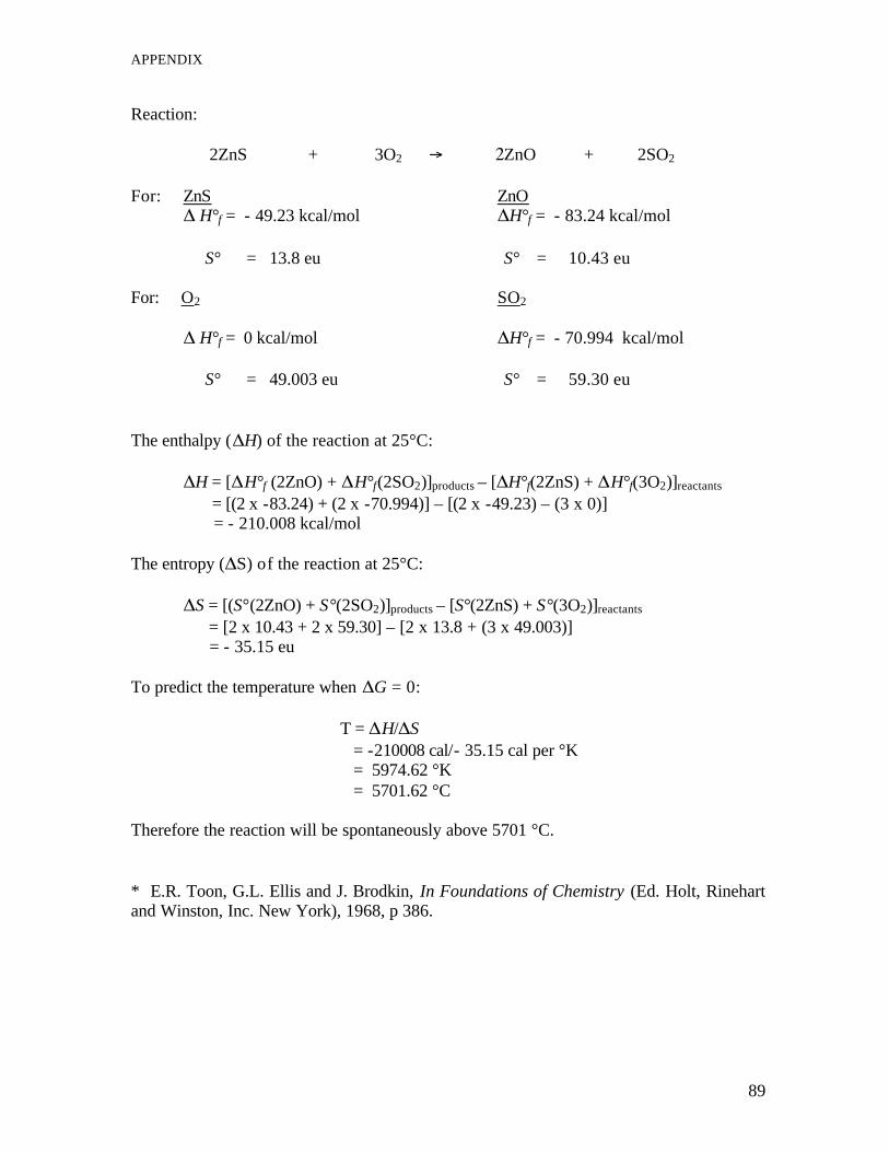
APPENDIX
89
Reaction: 2ZnS + 3O2 → 2ZnO + 2SO2 For: ZnS ZnO
∆ H°f = - 49.23 kcal/mol ∆H°f = - 83.24 kcal/mol S° = 13.8 eu S° = 10.43 eu For: O2 SO2
∆ H°f = 0 kcal/mol ∆H°f = - 70.994 kcal/mol S° = 49.003 eu S° = 59.30 eu The enthalpy (∆H) of the reaction at 25°C: ∆H = [∆H°f (2ZnO) + ∆H°f(2SO2)]products – [∆H°f(2ZnS) + ∆H°f(3O2)]reactants
= [(2 x -83.24) + (2 x -70.994)] – [(2 x -49.23) – (3 x 0)] = - 210.008 kcal/mol The entropy (∆S) of the reaction at 25°C: ∆S = [(S°(2ZnO) + S°(2SO2)]products – [S°(2ZnS) + S°(3O2)]reactants
= [2 x 10.43 + 2 x 59.30] – [2 x 13.8 + (3 x 49.003)] = - 35.15 eu
To predict the temperature when ∆G = 0:
T = ∆H/∆S = -210008 cal/- 35.15 cal per °K = 5974.62 °K = 5701.62 °C Therefore the reaction will be spontaneously above 5701 °C. * E.R. Toon, G.L. Ellis and J. Brodkin, In Foundations of Chemistry (Ed. Holt, Rinehart and Winston, Inc. New York), 1968, p 386.

Kenneth Thembela Hillie: PhD thesis
90
LIST OF FIGURES Figure 1.1 (p. 3) shows the cross-sectional view of the field emission cathodes (FED) Figure 2.1 (p. 12) shows models of electron transitions resulting in luminescence Figure 2.2 (p. 13) shows the schematic presentation of the luminescence process in ZnS:Cu,Al,Au phosphor Figure 2.3 (p. 18) shows the configuration co-ordinate model of a luminescent centre Figure 3.1 (p. 29) shows the cross sectional schematics of the heating (a) and cooling (b) set-ups. Figure 4.1 (p. 36) shows the APPHs of S, C, O and Zn as well as the CL measured at a current density of 88 mA cm-2 as a function of Coulomb dose. Figure 4.2 (p. 37) shows the APPHs of S, C, O and Zn as well as the CL measured at a current density of 2.5 mA cm-2 as a function of Coulomb dose. Figure 4.3 (p. 37) shows the normalised APPHs of sulphur at different electron current densities as a function of Coulomb dose. Figure 4.4 (p. 39) shows the normalised CL intensities measured at different electron current densities as a function of Coulomb dose. Figure 5.1 (p. 44) shows the APPHs of S, C x 5, O and Zn as well as the CL as a function of Coulomb dose measured at a current density of 88 mA/cm2 at temperatures of (a) 46 °C, (b) 200 °C and (c) 300 °C as indicated. Figure 5.2 (p. 45) shows the CL intensity as function of temperature at a pressure of 2 x 10⁻⁹ Torr before any degradation. Figure 5.3 (p. 46-47) shows the APPHs of S, O and Zn as function of Coulomb dose measured at a current density of 88 mA/cm2 at temperatures of (a) 48 °C and (b) 310 °C as indicated. (c) At 210°C shows the S APPHs of a continuous e-beam bombardment and of a bombardment with e-beam shut off intervals, after sputtering. Figure 5.4 (p. 48) shows the Coulomb doses required to reach 60% of the original S signal as function of temperature Figure 6.1 (p. 54) shows the RBS spectrum of pulsed laser deposited ZnS phosphor film on Si (100), the dotted line is the ZnS 1:1 compositional simulation. Figure 6.2 (p. 55) shows the AES differential energy spectra of (a) first layer before sputtering, (b) sample 1 and (c) sample 4, both during sputtering. Figure 6.3 (p. 56) shows the AES depth profiles of (a) sample 1 and (b) sample 4 Figure 6.4 (p. 56) shows three dimensional AFM images of the ZnS films deposited on Si (100), (a) Sample 1 and (b) Sample 4. Figure 6.5 (p. 57) shows the statistical presentation of calculated rms roughness (Rrms) values for all the films. Figure 6.6 (p. 58) shows the film thickness values from the RBS measurements Figure 6.7 (p. 59) shows XRD spectra of the films, (a) sample 1, (b) sample 2, (c) sample 3 and (d) sample 4. (e) Is a spectrum of the target material. Figure 7.1 (p. 63) shows AES differential energy spectra of (a) film before degradation, (b) and (c) film after degradation for a Coulomb dose of about 300 C/cm2 in O2 and CO2, respectively. Figure 7.2 (p. 64) shows the APPHs of S, C, O, and Zn as well as the CL measured during degradation in an O2 ambient (a) and a CO2 ambient (b). Figure 7.3 (p. 66) shows the normalised APPH of sulphur for different electron beam energies as a function of Coulomb dose. Figure 7.4 (p. 67) shows the CL intensity at different electron beam energies Figure 8.1 (p. 70) shows the XRD spectrum of CdO bulk precipitate on a glass substrate. Figure 8.2 (p. 71) shows SEM images of a ZnS:Cu,Au,Al thin film (a) and a CdO coated ZnS:Cu,Au,Al thin film (b). Figure 8.3 (p. 72) shows Auger spectra before and after degradation in an O2 ambient for 470 C/cm2. Figure 8.4 (p. 73) shows APPHs of Cd, O, C, S, Cl and Zn as well as the CL measured during degradation in an O2 ambient as function of Coulomb dose Figure 8.5 (p. 75) shows the normalised CL intensity measured during degradation for (a) coated and (b) bare ZnS:Cu,Au,Al thin film phosphor as a function of Coulomb dose. Figure 9.1 (p. 79) shows the normalised S APPHs as a function of Coulomb dose acquired at (a) room temperature without cooling, (b) at –125 °C without cooling, (c) –125 °C with cooling and (d) room temperature with cooling. Figure 9.2 (p. 81) shows the TL glow curves of (a) the reference sample and (b) the degraded sample.

BIBLIOGRAPHY
91
BIBLIOGRAPHY Degrees: BSc, BSc Hons, MSc (cum laude)
Presentations in international conferences: 1. The Growth of Cu films on SiO2 by atmospheric pressure Metalorganic Vapour Phase Epitaxy (MOVPE) at the Sixth European Workshop on Metal -Organic vapour phase epitaxy and related growth techniques. Gent, Belgium June 1995. G. Scriven, K.T.Hillie, A. Leitch, V.V.Kozyrkov and C.M.Demanet 2. Investigation of various cleaning procedures of transparent conducting oxide substrate for CdS/CdTe photovoltaic cells using Scanning Force Microscopy. Presented at the Fourth Workshop on Industrial Applications of Scanned Probe Microscopy, Gaithersburg (Md), 6-8 May 1997. C.M. De manet, K.T. Hillie, J.M. Nel, F.D. Auret and H.L.Gaigher 3. AFM, LFM and Force Modulation assessment of cleaning procedures on metal oxide on glass substrate for photovoltaic applications, at the 7th European Conference on Applications of Surface and Interface Analysis, Gothenborg, Sweden. 16-20 June 1997. K.T. Hillie, C.M. Demanet, J.M. Nel and F.D. Auret 4. Effect of Cleaning Procedures on the Quality of Palladium Schottky Barrier Diodes Fabricated on Epitaxially Grown n-Si, at the 7th European Conference on Applications of Surface and Interface Analysis, Gothenborg, Sweden 16-20 June 1997. K.T. Hillie, C.M. Demanet, P.N.K. Deenapanray, F.D.Auret and G. Myburg 5. Degradation of FED phosphors. At the 8th European Conference on Applications of Surface and Interface Analysis, Sevilla, Spain 4-8 October 1999. H.C. Swart and K.T. Hillie 6. On the degradation of ZnS:Cu,Al,Au phosphor powder: the effects of temperature, 14th International Conference on Defects in Insulating Materials (ICDM), Johannesburg-Midrand, South Africa 3-7 April 2000. K.T. Hillie and H.C. Swart 7. The effect of temperature on the degradation of ZnS FED phosphors, presented at APSIAC'2000, Beijing, China 2000. H.C. Swart, K.T. Hillie and A.P. Greeff.
Presentations in local conferences: 1. Experimental determination of the shape and radius of Atomic Force Microscope tips. July 1994 at the SAIP* Annual Conference in Mmabatho RSA. K.T. Hillie and C.M.Demanet 2. Atomic Force Microscope Investigation of Chemical Vapour Deposited Cu film on SiO2 (June 1995) At the SAIP* annual Conference in Cape Town RSA. K.T. Hillie and C.M.Demanet.

Kenneth Thembela Hillie: PhD thesis
92
3. Scanning Force Microscope investigation of various methods of cleaning conducting oxide substrates on glass for photovoltaic cell. July 1996 at the Annual SAIP* Conference in Pretoria RSA. K.T.Hillie, C.M. Demanet, J.M. Nel and F.D Auret 4. AFM characterisation of the morphological properties of the chalchopyrites CuInSe2 and Cu(In,Ga)Se2 absorber layers for photovoltaic applications. At the annual SAIP* conference in Cape Town, July 1998. K.T. Hillie, C.M. Demanet, and V.Alberts. 5. The effect of current density on the degradation of ZnS:Cu,Al,Au phosphor powders under electron bombardment. At the annual SAIP* conference in Port Elizabeth, 03-09 July 1999. K.T. Hillie, G.L.P. Berning and H.C. Swart 6. Influence of Substrate morphology and temperature on Electrodeposited CdS thin films. At the SAIP* annual conference in Port Elizabeth RSA, 1999. J.M. Nel, M. van Staden, G. Myburg, K.T. Hillie, C.M. Demanet, C.W. Louw, H.L.Gaigher and F.D. Auret. 7. The effect of temperature on the degradation of ZnS FED phosphors. At the annual SAIP* conference in Johannesburg, July 2000. K.T. Hillie, H.C. Swart, and A.P. Greeff 8. ZnS thin films grown on Si(100) by XeCl pulsed laser ablation. At the annual SAIP* conference in Johannesburg, July 2000. K.T. Hillie and H.C. Swart. 9. Electron beam induced degradation of a ZnS:Cu,Au,Al thin film phosphor on Si(100) substrate, At the annual SAIP* conference in Durban, July 2001. K.T. Hillie and H.C. Swart SAIP* - South African Institute of Physics Manuscripts appearing in conference proceedings: 1. The Growth of Cu films on SiO2 by atmospheric pressure Metalorganic Vapour Phase Epitaxy (MOVPE). Workshop Booklet. EW MOVPE VI. 6th European Workshop on Metal Organic Vapour Phase Epitaxy and Related Growth Techniques, A 20, 1995. G. Scriven, K.T.Hillie, A. Leitch V.V.Kozyrkov and C.M.Demanet 2. Effect of Cleaning Procedures on the Quality of Palladium Schottky Barrier Diodes Fabricated on Epitaxially Grown n-Si. Proceedings of the 7th European Conference on Applications of Surface and Interface Analysis (ECASIA’97), p511, 1997. K.T. Hillie, C.M. Demanet, P.N.K. Deenapanray, F.D. Auret, G. Myburg. 3. AFM, LFM and Force Modulation assessment of cleaning procedures on metal oxide on glass substrate for photovoltaic applications. Proceedings of the 7th European Conference on Applications of Surface and Interface Analysis (ECASIA’97), p583, 1997. K.T. Hillie, C.M. Demanet, J.M. Nel, F.D. Auret. 4. Characterisation of polycrystalline CuInSe2 thin films by atomic force microscopy imaging. Proceedings of the 37th Annual Conference of the Microscopy Society of Southern Africa (MSSA), 29, 1998. V. Alberts, K.T. Hillie and C.M. Demanet.

BIBLIOGRAPHY
93
Publications in international Journals: 1. Using scanning force microscopy (SFM) to investigate cleaning procedures of different transparent conducting oxide substrates. Applied Surface Science, 134, 22-30, 1998. J.M. Nel, K.T. Hillie, C.M.Demanet, F.D. Auret and H.L. Gaigher 2. Atomic Force Microscopy Study of Si(111) Surface Morphology and Electrical Characteristics of Pd/n-Si Schottky Diodes: Effect of Cleaning Procedures. Surface and Interface analysis, 26, 748-757, 1998. P.N.K. Deenapanray, K.T. Hillie, F.D. Auret, G.Myburg and C.M. Demanet. 3. Atomic Force Microscopy and High-resolution RBS Investigation of the Surface Modification of Magnetron Sputter-etched Si(111) in an Argon Plasma at Different Pressures. Surface and Interface analysis, 27, 881-888, 1999. P.N.K. Deenapanray, K.T. Hillie, C.M. Demanet and M.C. Ridgway. 4. Degradation of ZnS FED Phosphors. Surface and Interface Analysis, 30, 383, 2000. H.C. Swart and K.T. Hillie. 5. Atomic force microscopy imaging of polycrystalline CuInSe2 thin films. Journal of Microscopy-Oxford, 197, 206-215, 2000. V. Alberts, K.T. Hillie and C.M. Demanet 6. On the degradation of ZnS:Cu,Al,Au phosphor powder: The effects of temperature, Radiation Effects and Defects in Solids, 154 (3-4), 373-376, 2001. K.T. Hillie and H.C. Swart 7. ZnS thin films grown on Si(100) by XeCl pulsed laser ablation. Applied Surface Science, 177 (1-2), 73-77, 2001. K.T. Hillie, C. Curren and H.C. Swart 8. The effect of temperature on the degradation of ZnS FED phosphors. Surface and Interface Analysis, 32, 110-113, 2001. H.C. Swart, K.T. Hillie and A.P. Greeff 9. Electron beam induced degradation of a pulsed laser deposited ZnS:Cu,Au,Al thin film on a Si(100) substrate. Applied Surface Science, 183, 304-307, 2001. K.T. Hillie and H.C. Swart 10. Effect of a CdO coating on the degradation of a ZnS thin film phosphor material. Applied Surface Science. 187, 139-146, 2002. K.T. Hillie, S.S. Basson and H.C. Swart 11. Low temperature effect on the electron beam induced degradation of ZnS:Cu,Au,Al phosphor powders Applied Surface Science. Submitted. K.T. Hillie and H.C. Swart
Recommended