Dielectric breakdown and failure of anodic aluminum oxide films forelectrowetting systemsM. Mibus, C. Jensen, X. Hu, C. Knospe, M. L. Reed et al. Citation: J. Appl. Phys. 114, 014901 (2013); doi: 10.1063/1.4812395 View online: http://dx.doi.org/10.1063/1.4812395 View Table of Contents: http://jap.aip.org/resource/1/JAPIAU/v114/i1 Published by the AIP Publishing LLC. Additional information on J. Appl. Phys.Journal Homepage: http://jap.aip.org/ Journal Information: http://jap.aip.org/about/about_the_journal Top downloads: http://jap.aip.org/features/most_downloaded Information for Authors: http://jap.aip.org/authors
Downloaded 02 Jul 2013 to 128.143.23.241. This article is copyrighted as indicated in the abstract. Reuse of AIP content is subject to the terms at: http://jap.aip.org/about/rights_and_permissions
Dielectric breakdown and failure of anodic aluminum oxide films forelectrowetting systems
M. Mibus,1 C. Jensen,2 X. Hu,3 C. Knospe,4 M. L. Reed,3 and G. Zangari1,a)
1Department of Materials Science and Engineering, University of Virginia, Charlottesville, Virginia 22904, USA2Department of Chemical Engineering, University of Virginia, Charlottesville, Virginia 22904, USA3Department of Electrical and Computer Engineering, University of Virginia, Charlottesville, Virginia 22904, USA4Department of Mechanical and Aerospace Engineering, University of Virginia, Charlottesville,Virginia 22904, USA
(Received 3 April 2013; accepted 13 May 2013; published online 2 July 2013)
We study electrical properties and breakdown phenomena in metal/aluminum oxide/metal and
electrolyte/aluminum oxide/metal contacts, with the aim to achieve a better understanding of
failure modes and improve the performance of model electrowetting systems. Electrical conduction
in anodic aluminum oxide dielectrics is dominated by the presence of electrically active trapping
sites, resulting in various conduction mechanisms being dominant within distinct voltage ranges
until hard breakdown occurs. Breakdown voltage depends on its polarity, due to the formation of a
p-i-n junction within the oxide; such asymmetric behavior tends to disappear at larger oxide
thickness. Electrolyte/dielectric contacts present an even more pronounced asymmetry in
breakdown characteristics: a cathodic bias results in breakdown at low voltage, while under anodic
bias high field ionic conduction starts before breakdown occurs. These phenomena are interpreted
in terms of electrochemical reactions occurring at the surface: cathodic processes contribute to
oxide dissolution and failure, while anodic processes result in additional oxide growth before
breakdown. VC 2013 AIP Publishing LLC. [http://dx.doi.org/10.1063/1.4812395]
INTRODUCTION
Electrowetting on dielectric, or EWOD, refers to the
change in apparent contact angle when a voltage is applied
between a liquid drop and a surface. The use of a dielectric
in place of a conductive surface allows the application of
large voltages while avoiding electrolysis of the fluid.1 An
EWOD device can therefore operate over a large voltage
range allowing for significant contact angle change without
the onset of spurious effects. EWOD has been successfully
exploited in various microfluidic devices including electro-
des to move and mix fluids,2,3 electrically controllable mi-
crolenses,4 light transmission through optical fibers,5
reflective displays for electronic paper,6 and capillary force
actuators.7 To first order, the voltage dependence of the con-
tact angle is quantified by the Young-Lippmann equation
cosðhÞ ¼ cosðh0Þ þ1
cLG
1
2
ere0
tV2; (1)
where h is the apparent contact angle of the liquid with
applied voltage, h0 is the equilibrium contact angle, clg is the
surface tension at the gas-liquid interface, er is the dielectric
constant of the dielectric layer, e0 is the permittivity of free
space, t its thickness, and V is the applied voltage. The per-
formance of current EWOD systems is limited by the use of
relatively thick (�10�6 m) dielectric films, which according
to Eq. (1) require a high voltage to achieve appreciable
changes in contact angle.8 The most direct means to mini-
mize the voltage applied during operation is to increase the
dielectric layer capacitance by using a thinner layer and/or
materials with high dielectric constant. One concern with the
former approach is that by reducing dielectric thickness, the
electric field across this layer would increase, magnifying its
susceptibility to breakdown and failure. The use of materials
with high dielectric constant, on the other hand, is a promis-
ing avenue to enhance device performance. Another limita-
tion of current EWOD systems is contact angle saturation,
which is observed at high voltages and has been also linked
to the onset of breakdown phenomena;9,10 delaying or alto-
gether avoiding breakdown would therefore result in larger
contact angle variation, enhanced performance, and
increased reliability.
In order to achieve large values of h0 and large changes
in h, actual EWOD systems require a hydrophobic coating in
direct contact with the liquid; when using an oxide film as
dielectric the wetting angle at equilibrium would be low, and
a fluoropolymer layer must thus be added to the film stack.11
This work is mostly focused on the dielectric properties of
the oxide, and in order to simplify the system under study we
avoid using a hydrophobic topcoat; we show however that
addition of such topcoat has the effect of further delaying the
onset of breakdown phenomena.
Several valve metal oxides exhibit high values of the
bulk dielectric constant: Al2O3(er¼ 9), Ta2O5(er¼ 22), ZrO2,
and HfO2(er¼ 25).12 These oxides can be grown by film dep-
osition methods, using sputtering or evaporation, or can be
obtained by UV-assisted or electrochemical oxidation (anod-
ization) of metallic film precursors. Anodization entails
application of a positive voltage to a metal film immersed
in an appropriate electrolyte, converting the metal to the
corresponding metal oxide. This method presents several
a)Author to whom correspondence should be addressed. Electronic mail:
0021-8979/2013/114(1)/014901/8/$30.00 VC 2013 AIP Publishing LLC114, 014901-1
JOURNAL OF APPLIED PHYSICS 114, 014901 (2013)
Downloaded 02 Jul 2013 to 128.143.23.241. This article is copyrighted as indicated in the abstract. Reuse of AIP content is subject to the terms at: http://jap.aip.org/about/rights_and_permissions

advantages: anodization can be performed with simple
instrumentation at low temperatures, and, in addition, setting
the applied voltage gives precise control over the final thick-
ness of the oxide layer.
Electrochemical anodization of all valve metals has been
demonstrated;13 however, anodization of aluminum is by far
the best understood and most easily implemented. The nature
of the anodic film formed on aluminum depends mainly on
the anodization electrolyte: a thin and compact barrier layer14
is formed in neutral electrolytes where the oxide film is insol-
uble, while a porous structure15 is obtained in acidic electro-
lytes. In EWOD applications, a barrier layer is preferred since
its smoothness limits contact angle hysteresis. During the
anodization process, the oxide film grows via field-induced
migration of the metal ion and the oxygen anion in opposite
directions, resulting in growth occurring simultaneously at the
metal/oxide and oxide/electrolyte interface, where the two
species react. The final thickness of the oxide layer is propor-
tional to the anodization voltage, with a slope (anodization ra-
tio, AR) of �1.1 to 1.4 nm/V, depending on the anodization
solution.14 The resulting oxide is amorphous and therefore
presents a high density of point defects, such as vacancies,
interstitials and impurities from the electrolyte, all of which
may generate electrically active trapping sites within the ox-
ide. These defects are responsible for the (low) electronic con-
ductivity of dielectric oxide films.
Degradation and failure in EWOD systems either may
result from phenomena occurring at the liquid/dielectric
interface or may originate within the solid oxide, from the
accumulation of point defects generated by electron transport
through the dielectric; breakdown, consisting in a sudden
increase in conductivity and loss of functionality, is observed
when a critical density of defects is reached, sufficient to
form a percolative and conductive path between the electro-
des.16 Breakdown has been studied extensively in the solid
state on silicon oxide, in the context of gate oxide degrada-
tion in CMOS,17 and more recently in Al,18 and high-edielectric films.19 In contrast, the current understanding of
degradation and failure at oxide/electrolyte interfaces is lim-
ited. An aluminum oxide/electrolyte interface is known to
exhibit rectification, with a cathodic polarization leading to
large currents.20 The phenomenon was ascribed to hydrogen
reduction occurring at the oxide surface, leading to proton
conduction within the oxide via defects in the film.21 This
reduction current may be accompanied by an additional ca-
thodic phenomenon, i.e., reduction of the oxide, leading
eventually to dissolution of the oxide.22 Stability of the oxide
film is further affected by the nature of the electrolyte anion,
with Cl� being especially harmful.23 More recently, Raj
et al.24 have demonstrated the importance of electrolyte
chemistry in enhancing the performance of CYTOP (Asahi
Glass), an amorphous fluoropolymer coating serving as a
hydrophobic topcoat, showing that the use of large size cati-
ons and anions hinders dielectric failure. The deleterious
effect of polarity and Cl� has been further confirmed in
Ta2O5 EWOD devices, where a positive bias resulted in a
quicker and irreversible decrease in contact angle.25
In this report we investigate breakdown and dielectric
failure of anodized aluminum oxide barrier films with
thicknesses ranging from 20 to 60 nm. To this end, we use
both an all solid state metal/oxide/metal (MOM) contact and
an electrolyte/oxide/metal (EOM) contact to compare and
contrast failure due to conduction within the oxide with that
due to electrochemical processes at the interface. We find that
MOM contacts exhibit non-linear, asymmetric characteristics,
due to an asymmetric charge distribution in the oxide; sharp
breakdown is observed at potentials which increase with oxide
thickness. EOM contacts present a more pronounced asymme-
try in their I-V characteristics and fail in correspondence of
the onset of charge transfer reactions at the surface.
EXPERIMENTAL SECTION
Materials
Aluminum films of 100 nm thickness were grown by
e-beam evaporation (CHA Industries, Fremont, CA) onto the
native surface of a Si wafer, pre-coated with a 5 nm thick
titanium adhesion layer. Aluminum anodization was per-
formed at room temperature in a two electrode electrochemi-
cal cell with the electrodes in a vertical configuration, using
a platinum mesh counter electrode. The anodization solution
was 30 wt. % ammonium pentaborate (NH4B5O8) in 99.99%
ethylene glycol. The anodization voltage, V, varied from
10 V to 40 V. The thickness of the resulting barrier film
depends upon V and is calculated by the anodizing ratio
(nm/V).
MOM contacts were obtained by depositing a 100 nm
thick Aluminum film with e-beam evaporation on top of the
Al oxide barrier layer. Eight independent Al contacts with
0.80 mm2 area were grown at distinct locations on the oxide
using a shadow mask. EOM contacts were prepared by care-
fully positioning a 1.5 ll droplet of a.05 M sodium sulfate so-
lution on the oxide surface with a pipette.
All solutions described above were prepared from Milli-
Q water (resistivity 18.2 MX cm), using chemicals from
Sigma-Aldrich with >99% purity.
Film characterization
The oxide thickness was measured with a spectroscopic
ellipsometer (HORIBA Jobin Yvon, Irvine, CA); the mea-
surement was performed at several points across the film
area, showing less than 1% variation. Thickness was further
confirmed by monitoring the charge density Q passed during
the anodization process and using t¼QM/zFq, where M is
the atomic weight of the oxide, z the number of transferred
electrons in an elementary reaction, F Faradays’ constant,
and q the oxide density. Surface morphology of the films
was investigated with a field emission scanning electron
microscope (JEOL 6700F).
The current-voltage characteristics were recorded in
both the MOM and EOM configurations using two probes
controlled through a HP 4145b semiconductor property ana-
lyzer. Data were collected at 0.1 V intervals while sweeping
the voltage at a rate of 0.1 V/s. Probe positioning was con-
trolled through a Micromanipulator 7000 probe station with
gold plated probe needles. In the following, a bias will be
014901-2 Mibus et al. J. Appl. Phys. 114, 014901 (2013)
Downloaded 02 Jul 2013 to 128.143.23.241. This article is copyrighted as indicated in the abstract. Reuse of AIP content is subject to the terms at: http://jap.aip.org/about/rights_and_permissions

designated as positive if a positive voltage is applied to the
Al contact (MOM) or to the electrolyte (EOM).
RESULTS AND DISCUSSION
Oxide growth
Figure 1 shows the aluminum oxide thickness, as deter-
mined by ellipsometry, vs. anodization voltage. As expected
the relationship is approximately linear, with an anodizing ratio
of �1.2 nm/V. The sample anodized at 10 V shows a positive
deviation from the extrapolated linear trend; this behavior is
ascribed to a change in the ionic migration process, dominated
at low voltage by ion injection in the oxide, and at higher volt-
age by bulk ion migration, leading to an increase in average
growth rate at larger thickness.14 On the same grounds, the
extrapolation at low voltages should not be taken literally, since
under these conditions both ion migration and diffusion may
contribute to ionic transport. The oxide films are very smooth
and continuous, as determined by SEM imaging.
Metal-oxide-metal contacts
Current-voltage I-V characteristics for MOM contacts
were recorded for various oxide film thickness and typical
results are reported in Fig. 2(a). The characteristics are
highly non-linear and are asymmetrical with respect to polar-
ity, with the positive polarity (positive voltage applied to the
top Al contact) always showing breakdown at a lower volt-
age. A sharp, hard breakdown, leading to a steep current
increase up to the maximum current allowed by the available
instrumentation, is observed in all cases. The electrical
behavior of the oxide is reversible if the applied voltage is
maintained below the breakdown voltage VB, but the
changes in conductivity are irreversible if the region of
breakdown is reached. Fig. 2(b) reports VB and the corre-
sponding breakdown field EB¼VB/t, measured under both
polarities as a function of the oxide film thickness. For each
sample, the error bars identify the highest and lowest value
of VB, EB measured on that sample, and the symbols repre-
sent the average value. It is noted that both the scatter in VB,
EB and the difference between VBþ(EBþ) and VB�(EB�)
decrease with increasing thickness (i.e., increasing anodiza-
tion voltage).The breakdown field for the oxides ranges
between 3-7 MV/cm with the value leveling to 7 MV/cm in
both polarities with increasing film thickness (Fig. 2(b)),
similar to the values observed in other anodic aluminum
oxide films,26 but higher than thermally oxidized
aluminum(5 MV/cm).18
The observed asymmetry in the I–V characteristics can
be traced back to an asymmetry in the Al oxide film struc-
ture. During anodization, the large electric field in the oxide
causes injection of metal ions from the metal side, and of
anions from the electrolyte (O2�, OH�, borate), into the ox-
ide. Opposite gradients in the concentration of both cations
and anions are therefore present within the oxide, leading to
the formation of a p-intrinsic-n (p-i-n) junction, where the p
and n region are about 5 nm thick and their doping polarity is
determined by an excess of anions and cations, respec-
tively.27 The presence of a p-i-n junction naturally leads to
asymmetric characteristics; in addition, the degree of asym-
metry would decrease with increasing oxide thickness since
under these conditions the intrinsic region makes up most of
the oxide thickness and would dominate the electrical behav-
ior. Under positive bias the p-i-n junction is forward biased,
and the resulting current is larger. A larger current flowing
through the oxide would accelerate the breakdown process,
leading to a lower breakdown voltage, as observed. It should
be noticed also that during anodization the sample is sub-
jected to negative bias polarization, according to the defini-
tion adopted here; the fact that a higher breakdown voltage
is observed under these conditions suggests therefore that
transport of charges becomes more difficult when the oxide
is subject to the same bias present during anodization.
Electronic conduction processes in MOM contacts
The highly defected structure of anodized Al oxide gives
rise to localized excess or deficit of oxygen, Al, or impurities,
yielding a high density of trapped charges which act as electri-
cally active defects.28–30 The defect concentration has been
quantified for a wide variety of passive metal films, yielding
values in the range of 1018-1020 cm�3.31 Specific values for
aluminum oxide barrier layers have recently been measured at
1018-1019 cm�3, depending on thickness.32 Significant elec-
tronic conductivity may therefore be present, and various elec-
tronic conduction processes become thus possible.33 These
include Schottky emission (SE), Poole-Frenkel emission (PF),
and Fowler-Nordheim tunneling (FN);34 the total electronic
current would therefore be j¼ jSEþ jPFþ jFN.
Schottky emission consists in the injection of thermally
activated carriers from a metal contact into the oxide through
a potential barrier u lowered by an applied electric field.
Deformation of this barrier due to image charges is limited
in high-e materials; therefore, this effect should not be as im-
portant as in SiO2. However, due to the highly defective na-
ture of the metal oxide layer interface, the barrier could be
reduced even for weak image charge effects. jSE is described
by the Schottky-Richardson equation for thermionic
emission35
FIG. 1. Thickness of anodized aluminum oxide films vs. anodization volt-
age. Thickness measurements by ellipsometry are in close agreement with
calculations from the charge density.
014901-3 Mibus et al. J. Appl. Phys. 114, 014901 (2013)
Downloaded 02 Jul 2013 to 128.143.23.241. This article is copyrighted as indicated in the abstract. Reuse of AIP content is subject to the terms at: http://jap.aip.org/about/rights_and_permissions

lnðJÞ ¼ b2kT
ffiffiffiEpþ lnðAT2Þ � q/
kT; (2)
b ¼ q3
4pere0
; (3)
where b quantifies the barrier reduction, E is the electric
field, T the temperature, A is a constant, and the other sym-
bols have the usual meaning. Fitting ln jSE vs. sqrt(E) allows
determination of er. The resulting value is 10.7 with minimal
variance across thicknesses, comparable to the reported
range of 7-12.8 for anodic Al2O3.13
Poole-Frenkel emission describes charge injection
between localized charged trap sites, again triggered by a
field-induced reduction of the energy barrier, which leads to
hopping processes. P-F emission is particularly relevant for
oxide thickness above 25 nm, where the relative importance
of Schottky emission would decrease. The Poole-Frenkel
current is described by Eq. (4)
lnJ
E
� �¼ b
2kT
ffiffiffiEpþ lnðCÞ; (4)
where C represents a proportionality constant for the conduc-
tivity in the absence of electric field. Fitting a linear relation-
ship to ln(j/E) vs. sqrt(E) provides again an estimate of the
dielectric constant, yielding a value between 10 and 15, inde-
pendent of thickness. This current saturates when the applied
field is sufficient to remove all charges from their traps.
Under these conditions the bending of the energy barrier is
very large, increasing the probability of tunneling.
Fowler-Nordheim tunneling defines tunneling through a
barrier reduced by an applied electric field. The equation
describing this phenomenon is
FIG. 2. (a) I–V characteristics for alu-
minum oxide films of various thickness
in a metal-oxide-metal configuration
operating under both polarities. (b)
Breakdown voltage VB and breakdown
field EB vs. film thickness for positive
(black, square) or negative (red, trian-
gle) polarity applied to the top contact.
The error bars represent max and min
values for the data scatter with the av-
erage value as the data point.
014901-4 Mibus et al. J. Appl. Phys. 114, 014901 (2013)
Downloaded 02 Jul 2013 to 128.143.23.241. This article is copyrighted as indicated in the abstract. Reuse of AIP content is subject to the terms at: http://jap.aip.org/about/rights_and_permissions
lnJ
E2
� �¼ lnðAÞ � B
E; (5)
where
A ¼ mq3
m�8ph/;
B ¼ 8p3
2m�
h2
� �1=2/3=2
q:
A and B are constants dependent on the metal-insulator bar-
rier u and the electron effective mass in the oxide m*. FN
tunneling describes the high field conduction region just
before the onset of breakdown.
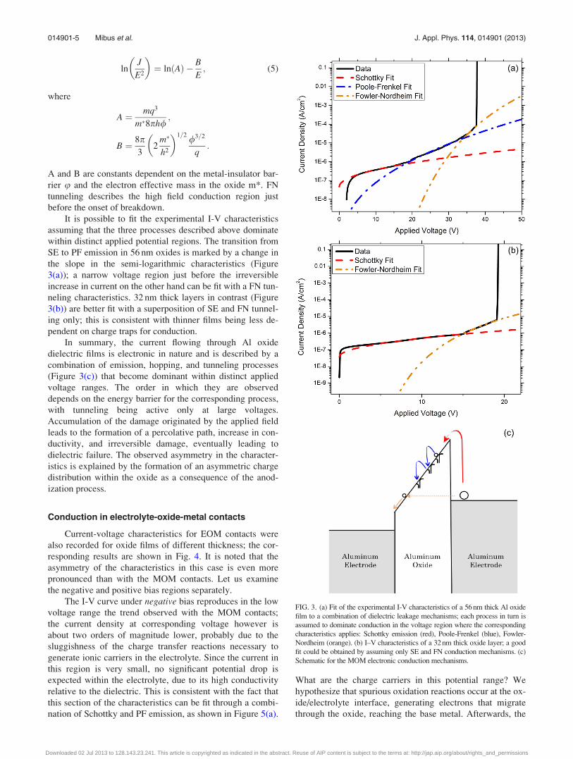
It is possible to fit the experimental I-V characteristics
assuming that the three processes described above dominate
within distinct applied potential regions. The transition from
SE to PF emission in 56 nm oxides is marked by a change in
the slope in the semi-logarithmic characteristics (Figure
3(a)); a narrow voltage region just before the irreversible
increase in current on the other hand can be fit with a FN tun-
neling characteristics. 32 nm thick layers in contrast (Figure
3(b)) are better fit with a superposition of SE and FN tunnel-
ing only; this is consistent with thinner films being less de-
pendent on charge traps for conduction.
In summary, the current flowing through Al oxide
dielectric films is electronic in nature and is described by a
combination of emission, hopping, and tunneling processes
(Figure 3(c)) that become dominant within distinct applied
voltage ranges. The order in which they are observed
depends on the energy barrier for the corresponding process,
with tunneling being active only at large voltages.
Accumulation of the damage originated by the applied field
leads to the formation of a percolative path, increase in con-
ductivity, and irreversible damage, eventually leading to
dielectric failure. The observed asymmetry in the character-
istics is explained by the formation of an asymmetric charge
distribution within the oxide as a consequence of the anod-
ization process.
Conduction in electrolyte-oxide-metal contacts
Current-voltage characteristics for EOM contacts were
also recorded for oxide films of different thickness; the cor-
responding results are shown in Fig. 4. It is noted that the
asymmetry of the characteristics in this case is even more
pronounced than with the MOM contacts. Let us examine
the negative and positive bias regions separately.
The I-V curve under negative bias reproduces in the low
voltage range the trend observed with the MOM contacts;
the current density at corresponding voltage however is
about two orders of magnitude lower, probably due to the
sluggishness of the charge transfer reactions necessary to
generate ionic carriers in the electrolyte. Since the current in
this region is very small, no significant potential drop is
expected within the electrolyte, due to its high conductivity
relative to the dielectric. This is consistent with the fact that
this section of the characteristics can be fit through a combi-
nation of Schottky and PF emission, as shown in Figure 5(a).
What are the charge carriers in this potential range? We
hypothesize that spurious oxidation reactions occur at the ox-
ide/electrolyte interface, generating electrons that migrate
through the oxide, reaching the base metal. Afterwards, the
FIG. 3. (a) Fit of the experimental I-V characteristics of a 56 nm thick Al oxide
film to a combination of dielectric leakage mechanisms; each process in turn is
assumed to dominate conduction in the voltage region where the corresponding
characteristics applies: Schottky emission (red), Poole-Frenkel (blue), Fowler-
Nordheim (orange). (b) I–V characteristics of a 32 nm thick oxide layer; a good
fit could be obtained by assuming only SE and FN conduction mechanisms. (c)
Schematic for the MOM electronic conduction mechanisms.
014901-5 Mibus et al. J. Appl. Phys. 114, 014901 (2013)
Downloaded 02 Jul 2013 to 128.143.23.241. This article is copyrighted as indicated in the abstract. Reuse of AIP content is subject to the terms at: http://jap.aip.org/about/rights_and_permissions

slope of the I-V curve increases and the sharp breakdown
process observed in MOM contacts is replaced by a gradual
current increase which eventually approaches saturation. The
potential at which the slope increases corresponds closely to
the anodization voltage. Taking into account that a negative
bias for the EOM contact corresponds to an anodic bias for
the oxide, we hypothesize that the observed current in this
region is an ionic current I, which is described by an expo-
nential dependence of current on applied field, E,
I¼ a*exp(bE), where a and b are temperature dependent con-
stants;36 the anodization potential therefore roughly sepa-
rates the potential regions where electronic and ionic
conduction dominate, respectively (Figure 5(b)). By trigger-
ing ion transport, the high voltage should result in further ox-
ide growth by anodization (Fig. 5(c)). This is the process
proposed by Dhindsa et al.37 to accomplish self-healing of
dielectrics during electrowetting operation. The actual
growth of the oxide was confirmed by applying a negative
bias to a 56 nm thick oxide using an EOM contact, sweeping
the voltage up to the saturation region for the ionic current.
After rinsing the sample, its thickness was measured by
ellipsometry and found to be 57-59 nm, 5%-8% thicker than
before. The oxide thickness increased further when holding
the current in the flat I-V region. At even higher potentials
(above 40 V in Figure 5(b)), an additional increase in current
was observed, with concurrent gas evolution; this process
corresponds to oxygen formation by water oxidation.
The oxide growth and the onset of the breakdown pro-
cess at negative bias can be monitored by sweeping the volt-
age on the same sample over several cycles while varying
the maximum applied value. Fig. 6 shows the I-V character-
istics of an EOM contact with a 38 nm thick oxide, up to the
point where ionic current flows and the current saturates
(Run 1). The second sweep is run up to the potential region
where oxygen is evolved; in this case, the increase in current
slope indicating the transition from electronic to ionic con-
duction occurs at a higher potential, suggesting that a thicker
oxide has been formed. The third voltage sweep (Run 3),
recorded after oxygen evolution on the electrode has
occurred, shows a completely different behavior, with a large
current and gas evolution occurring at much lower potentials,
below 5 V. The onset of gas evolution cannot be determined
precisely; therefore, it is difficult to correlate gas evolution
and oxide breakdown; qualitatively, however, it is possible
to associate visible gas evolution with a relatively large cur-
rent, which would trigger anodic breakdown.
The choice of electrolyte affects I-V characteristics
under negative bias. Commonly, chloride based salt solutions
are used as the electrolyte in electrowetting testing;38 this
FIG. 4. The characteristic I–V curves for Al2O3 layers of different thickness.
Polarity refers to the voltage being applied to the .05M Na2SO4 electrolyte
drop, with the ground being the base aluminum layer.
FIG. 5. (a) Typical I–V characteristics from a negatively biased EOM con-
tact consisting of a 56 nm of oxide and a .05 M Na2SO4 droplet as the top
contact. The dielectric current leakage models are fitted to the data using
Eqs. (2) and (4). (b) Two regions of the negative polarity curve are identified
where the electronic and ionic current dominate, respectively; the transition
corresponds roughly to at the anodization voltage (c) schematic of the oxide/
electrolyte interface for the negatively biased system.
014901-6 Mibus et al. J. Appl. Phys. 114, 014901 (2013)
Downloaded 02 Jul 2013 to 128.143.23.241. This article is copyrighted as indicated in the abstract. Reuse of AIP content is subject to the terms at: http://jap.aip.org/about/rights_and_permissions
choice however is far from ideal. The harmful effect of
aggressive Cl� ions can in fact be seen in Figure 7, demon-
strating the earlier failure and increased variability of the
breakdown event. The influence of halide ions in pitting cor-
rosion is well established for passive films on aluminum.39
The proposed mechanisms include chloride ion migration
through oxygen vacancies40 or local oxide thinning due to
complex formation.41 The clear detrimental impact of chlor-
ides suggests that other solutions would provide better sys-
tem performance. In our investigation, sodium sulfate
provided a simple, reliable electrolyte that does not trigger
localized corrosion processes.
Under positive bias, the I-V characteristics exhibits an
early and sharp departure from the characteristics at negative
bias, suggesting that early breakdown is occurring already at
3–7 V. Failure seems to occur concomitantly with gas
(hydrogen) evolution, i.e., when charge transfer reactions
occur at the dielectric surface at a significant rate. Charge
transfer may occur via two mechanisms: electron transport
from the metal to the electrolyte, or cation or proton trans-
port in the opposite direction. At very low bias the I-V curve
follows that measured in the MOM contact, suggesting that
the electronic leakage current may be triggering the cathodic
reaction (water splitting and hydrogen evolution, or oxide
reduction and dissolution), generating thus protons which
may successively penetrate within and/or dissolve the oxide.
Raj et al.24 have shown that the size of the ions in the
electrowetting electrolyte may affect the breakdown process,
both under negative and positive bias. Following this lead we
have substituted Naþ (radius 0.13 nm) with Csþ (0.19 nm) or
dodecyltrimethylammonium DTAþ (3 nm––total chain
length). Figure 8 shows that substitution of Naþ with Csþ
results in a decrease of the leakage current by about two
orders of magnitude in the saturation region, and a delay in
the onset of gas evolution, which shifts from �5 V to �30 V.
Further enhancement is obtained by using DTAþ, which in
some cases does not show any gas evolution up to 40 V. The
shift in breakdown potential has been interpreted in terms of
ionic size and their diminished ability to penetrate the oxide
through defects or pinholes.24 The fact that breakdown is asso-
ciated with a sizable cathodic current, and gas evolution
FIG. 6. Three consecutive I–V characteristics recorded at a 38 nm thick ox-
ide surface using the same 0.05M Na2SO4 droplet for all curves. The curves
were run (black to red to blue) immediately following one another without
altering the configuration. Oxide thickening is observed between 1 and 2,
breakdown between 2 and 3.
FIG. 7. The influence of electrolyte anion on the oxide failure for EOM con-
tacts tested under negative polarity on 50 nm oxide.
FIG. 8. (a) Effect of cation substitution (Csþ or DTAþ instead of Naþ) in
the electrolyte on the breakdown of a 44 nm thick aluminum oxide layer in a
positively biased EOM contact. (b) Schematic of the oxide/electrolyte inter-
face under positive bias, showing the various conduction and electrochemi-
cal processes; the right panel depicts how the selective adsorption of DTAþ
may hinder gas evolution.
014901-7 Mibus et al. J. Appl. Phys. 114, 014901 (2013)
Downloaded 02 Jul 2013 to 128.143.23.241. This article is copyrighted as indicated in the abstract. Reuse of AIP content is subject to the terms at: http://jap.aip.org/about/rights_and_permissions

however suggests that the phenomenon may be more com-
plex: upon gas evolution protons are evolved
(H2Oþ e�)OH�þHad, where Had indicates atomic hydro-
gen adsorbed at the dielectric surface) and penetration of
atomic hydrogen through the oxide would occur at a much
faster rate than any other ion. We hypothesize instead that
large cations may preferentially adsorb at the surface under
cathodic polarization, delaying hydrogen formation, either by
affecting the double layer structure or––in the case of
DTAþ––by physically hindering water access (Figure 8(b)).
Preliminary data collected in a three electrode set-up show in
fact that hydrogen evolution from Cs2SO4 solution occurs at
an electrode potential more negative than from a Na2SO4 so-
lution of the same concentration.
In summary, the pronounced asymmetry in the I-V char-
acteristics of EOM contacts is due to a combination of the
asymmetry in charge distribution within the oxide and the
asymmetry of electrochemical processes occurring at the
dielectric surface. An anodic potential applied to the oxide
only increases its thickness through a supplementary anod-
ization process, which occurs at potentials larger than the
previous anodization voltage. On the contrary, a cathodic
bias of the dielectric surface tends to reduce and dissolve the
oxide; this can occur as soon as current flows through the ox-
ide, the latter process being made possible by the presence of
trapped charges.
The above findings suggest that in order to enhance the
electrowetting performance of dielectric/electrolyte systems,
research should be focused on (i) decreasing leakage current
by decreasing trapped charge density: A lower leakage cur-
rent will delay the onset of breakdown in a MOM contacts as
well as the onset of electrochemical processes in EOM con-
tacts, delaying breakdown; (ii) widening the potential win-
dow of stability of the electrolyte: if cathodic and anodic
electrolyte dissociation occur at more negative and more
positive potential, respectively, the onset of breakdown will
be delayed; (iii) identifying dielectric oxides that are thermo-
dynamically stable in the electrolyte of choice under electro-
wetting conditions.
CONCLUSION
This study has investigated the underlying causes of fail-
ure in thin anodic oxide films as model EWOD systems. The
leakage current in a solid state MOM contact is described by
a combination of Schottky emission, Poole-Frenkel emission
and Fowler-Nordheim tunneling, each process dominating
within distinct voltage ranges. I-V characteristics are asym-
metric and the breakdown voltage under opposite bias is dif-
ferent. This is a consequence of the anodic oxide growth
mechanism, which results in an inhomogeneous charge dis-
tribution within the oxide, generating in turn a p-i-n junction
with asymmetric conduction properties. An electrolyte/ox-
ide/metal contact shows an even more pronounced asymme-
try in the breakdown behavior under opposite voltage bias. A
cathodic bias results in hydrogen adsorption and evolution,
leading to oxide reduction and dissolution at low applied
voltage; the preferential adsorption of large cations may
decrease the density of available sites for hydrogen
adsorption or otherwise polarize hydrogen evolution, delay-
ing degradation. When the EOM system is polarized anodi-
cally, oxide growth resumes once the anodization voltage is
exceeded, and breakdown does not occur until oxygen evolu-
tion is observed under increasing field.
ACKNOWLEDGMENTS
This work was supported by NSF grant (No. CMMI-
1030868).
1B. Berge, C. R. Acad. Sci., Ser. II: Mec., Phys., Chim., Sci. Terre Univers
317, 157 (1993).2S. K. Cho, H. Moon, and C. Kim, Microelectromech. Syst. 12, 70 (2003).3V. Srinivasan, V. K. Pamula, and R. B. Fair, Lab Chip 4, 310 (2004).4B. Berge and J. Peseux, J. Eur. Phys. E 3, 159 (2000).5P. Mach, T. Krupenkin, S. Yang, and J. A. Rogers, Appl. Phys. Lett. 81,
202 (2002).6R. A. Hayes and B. J. Feenstra, Nature (London) 425, 383 (2003).7C. R. Knospe and H. Haj-Hariri, Mechatronics 22, 251 (2012).8H. Moon, S. K. Cho, R. L. Garrell, and C.-J. Kim, J. Appl. Phys. 92, 4080
(2002).9A. G. Papathanasiou and A. G. Boudouvis, Appl. Phys. Lett. 86, 164102
(2005).10A. G. Papathanasiou, A. T. Papaioannou, and A. G. Boudouvis, J. Appl.
Phys. 103, 034901 (2008).11E. Seyrat and R. A. Hayes, J. Appl. Phys. 90, 1383 (2001).12J. Robertson, Rep. Prog. Phys. 69, 327 (2006).13M. M. Lohrengel, Mater. Sci. Eng. R 11, 243 (1993).14J. W. Diggle, T. C. Downie, and C. W. Goulding, Chem. Rev. 69, 365
(1969).15J. P. O’Sullivan and G. C. Wood, Proc. R. Soc. A 317, 511 (1970).16J. H. Stathis, J. Appl. Phys. 86, 5757 (1999).17S. Lombardo, J. H. Stathis, B. P. Linder, K. L. Pey, F. Palumbo, and C. H.
Tung, J. Appl. Phys. 98, 121301 (2005).18J. Kolodzey, E. A. Chowdhury, T. N. Adam, I. Rau, J. O. Olowolafe, and
J. S. Suehle, IEEE Trans. Electron Devices 47, 121 (2000).19G. Ribes, J. Mitard, M. Denais, S. Bruyere, F. Monsieur, C. Parthasarathy, E.
Vincent, and G. Ghibaudo, IEEE Trans. Device Mater. Reliab. 5, 5 (2005).20H. Takahashi, K. Kasahara, K. Fujiwara, and M. Seo, Corros. Sci. 36, 677
(1994).21D. A. Vermilyea, J. Appl. Phys. 27, 963 (1956).22A. R. Despic, D. M. Dra�zic, J. Balak�sina, L. Gajic-Krstajic, and R. M.
Stevanovic, Electrochim. Acta 35, 1747 (1990).23H. H. Strehblow, in Corrosion Mechanisms in Theory and Practice, edited
by P. Marcus, 2nd ed. (Marcel Dekker, Inc., New York, 2002), pp. 243–286.24B. Raj, M. Dhindsa, N. R. Smith, R. Laughlin, and J. Heikenfeld,
Langmuir 25, 12387 (2009).25L. Huang, B. Koo, and C. C. J. Kim, in Proceedings of IEEE International
Conference MEMS, Paris, France, 2012, pp. 428–431.26K. Chari and B. Mathur, Thin Solid Films 75, 157 (1981).27Y. Sasaki, J. Phys. Chem. Solids 13, 177 (1960).28A. Despic and V. P. Parkhutik, in Modern Aspects of Electrochemistry,
edited by J. Bockris, R. White, and B. Conway (Plenum Press, New York,
1989), Vol. 20, pp. 401–503.29J. Lambert, C. Guthmann, C. Ortega, and M. Saint-Jean, J. Appl. Phys. 91,
9161 (2002).30T. W. Hickmott, J. Appl. Phys. 102, 093706 (2007).31J. W. Schultze and M. M. Lohrengel, Electrochim. Acta 45, 2499 (2000).32B. Benfedda, L. Hamadou, N. Benbrahim, A. Kadri, E. Chainet, and F.
Charlot, J. Electrochem. Soc. 159, C372 (2012).33T. W. Hickmott, J. Appl. Phys. 102, 093707 (2007).34D. S. Campbell and A. R. Morley, Rep. Prog. Phys. 34, 283 (1971).35J. G. Simmons, J. Phys. D 4, 613 (1971).36A. G€untherschulze and H. Betz, Z. Phys. 92, 367 (1934).37M. Dhindsa, J. Heikenfeld, W. Weekamp, and S. Kuiper, Langmuir 27,
5665 (2011).38F. Mugele and J.-C. Baret, J. Phys.: Condens. Matter 17, R705 (2005).39E. McCafferty, Corros. Sci. 45, 1421 (2003).40D. D. Macdonald, J. Electrochem. Soc. 139, 3434 (1992).41T. H. Nguyen and R. T. Foley, J. Electrochem. Soc. 127, 2563 (1980).
014901-8 Mibus et al. J. Appl. Phys. 114, 014901 (2013)
Downloaded 02 Jul 2013 to 128.143.23.241. This article is copyrighted as indicated in the abstract. Reuse of AIP content is subject to the terms at: http://jap.aip.org/about/rights_and_permissions
Recommended