UCRL-JRNL-217421
Direct Observations of Rapid Diffusion ofCu in Au Thin Films using In-Situ X-rayDiffraction
J. W. Elmer, T. A. Palmer, E. D. Specht
November 30, 2005
Journal of Vacuum Science and Technology - A

Disclaimer
This document was prepared as an account of work sponsored by an agency of the United States Government. Neither the United States Government nor the University of California nor any of their employees, makes any warranty, express or implied, or assumes any legal liability or responsibility for the accuracy, completeness, or usefulness of any information, apparatus, product, or process disclosed, or represents that its use would not infringe privately owned rights. Reference herein to any specific commercial product, process, or service by trade name, trademark, manufacturer, or otherwise, does not necessarily constitute or imply its endorsement, recommendation, or favoring by the United States Government or the University of California. The views and opinions of authors expressed herein do not necessarily state or reflect those of the United States Government or the University of California, and shall not be used for advertising or product endorsement purposes.

page 1
Direct Observations of Rapid Diffusion of Cu in Au Thin Filmsusing In-Situ X-Ray Diffraction
by:J. W. Elmer and T. A. Palmer
Lawrence Livermore National Laboratory, Livermore, CA, 94551, USA
E. D. SpechtOak Ridge National Laboratory, Oak Ridge, TN, 37831, USA
KeywordsSynchrotron Radiation, Interdiffusion, Grain Boundary Diffusion, Thin Films, Binary Alloys,
Activation Energy
AbstractIn-situ x-ray diffraction was performed while annealing thin-film Au/Cu binary diffusion
couples to directly observe diffusion at elevated temperatures. The temperature dependence of
the interdiffusion coefficient was determined from isothermal measurements at 700ºC, 800°C,
and 900ºC, where Cu and Au form a disordered continuous face centered cubic solid solution.
Large differences in the lattice parameters of Au and Cu allowed the initial diffraction peaks to
be easily identified, and later tracked as they merged into one diffraction peak with increased
diffusion time. Initial diffusion kinetics were studied by measuring the time required for the Cu
to diffuse through the Au thin film of known thickness. The activation energy for interdiffusion
was measured to be 65.4 kJ/mole during this initial stage, which is approximately 0.4x that for
bulk diffusion and 0.8x that for grain boundary diffusion. The low activation energy is attributed
to the high density of columnar grain boundaries combined with other defects in the sputter
deposited thin film coatings. As interdiffusion continues, the two layers homogenize with an
activation energy of 111 kJ/mole during the latter stages of diffusion. This higher activation
energy falls between the reported values for grain boundary and bulk diffusion, and may be
related to grain growth occurring at these temperatures which accounts for the decreasing
importance of grain boundaries on diffusion.

page 2
Introduction
Copper and gold are high conductivity metals used widely in the semiconductor industry
and elsewhere [1]. Thin Au coatings are sometimes used on Cu substrates to prevent oxidation
of the Cu and to enhance electrical conductivity, but these thin coatings can diffuse into the
copper substrate over periods of time, even at moderately low temperatures. Numerous studies
have investigated the diffusion of Au in Cu using different techniques such as tracer diffusion
[2], high resolution electron microscopy [3], x-ray diffraction [4], and Rutherford back-scattering
[5, 6]. The effects of grain boundaries and other defects have been investigated and are of
particular importance since they accelerate the diffusion rate [7-9].
At elevated temperatures, Cu and Au are mutually soluble and form a melting point
minimum at 910ºC [10], which makes this alloy combination useful to join the materials together
through a eutectic-type bonding method. However, due to the high diffusivity of Au in Cu at
elevated temperatures, thin-films of gold may diffuse into the copper during heating to the
bonding temperature, thus altering both the temperatures at which the liquid first forms and the
widths of the joints produced [11]. This study was undertaken to further investigate the diffusion
of Au into Cu using a synchrotron based x-ray diffraction technique in order to determine the
temperature dependence of the interdiffusion that occurs at elevated temperatures in Au-Cu thin
films. The in-situ synchrotron studies presented here are particularly useful in that they directly
track the initial rapid diffusion that takes place as the thin films intermix, as well as follow the
interdiffusion that takes place at longer times. The real-time information gathered from these
experiments reveals information about the kinetics and the mechanisms responsible for the
interfusion that takes place.
page 3
Experimental Procedures
Sample Preparation
The thin film samples were prepared by first depositing high purity Cu onto a stainless
steel substrate. A high purity Au layer was then deposited on top of the Cu layer to complete the
composite sample. This arrangement allowed carefully controlled layers of Au and Cu to be
deposited onto the stainless steel substrate so that the coated bar could be resistively heated to the
required temperatures. The stainless steel substrates consisted of rectangular bars that measured
100 mm long, 4.75 mm wide and 2 mm thick. These samples were machined from AISI type
304 stainless steel that was originally acquired in 100 mm diameter bar stock. Chemical analysis
was performed on the stainless steel showing it to contain (wt. %): 18.44% Cr, 10.71% Ni,
0.019% C, 0.053% N, 1.67% Mn, 0.04% Mo, <0.005%Nb, 0.46% Si, 0.04% V, 0.04% Cu,
0.02% Co, 0.016%S, 0.015% P, balance Fe (68.5%). One face of the stainless steel bar (4.75
mm x 100mm) was mechanically lapped to a finish of 0.1 µm rms in preparation for the coatings.
Prior to applying the coatings, the lapped stainless steel bar was first cleaned with acetone and
then wiped with ethanol to remove machining oils and contaminants.
The coatings were deposited on non-heated substrates using planar magnetron sputtering
in a vacuum chamber with base pressure in the 10-7 torr range. Five samples were prepared, all
coated together to provide identical starting conditions. The lapped and cleaned stainless steel
surface was first cleaned by ion milling with argon ions. They were then coated with a thin
(nominally 10.5 nm) flash of 99.995wt% Ti using one sputtering source in order to assist the
adhesion of the Cu to the stainless steel. This surface was then co-sputtered with Ti and
99.99wt% Cu from a second sputtering source to provide a thin (nominally 10.5 nm) transition
from the stainless steel to the pure Cu layer without breaking vacuum. The Ti source was then
turned off to deposit a 35 µm thick Cu layer on top of the Ti/Cu layer during a16 hr run. The

page 4
system was vented, the sputter target was changed and the sample stage was repositioned to
sputter deposit the Au layer.
After repositioning the substrates and installing the Au target, the system was pumped
down to a base pressure of 3.0X10⁻⁷ torr. The Cu-coated bars were ion-milled for 30 s in high
purity argon at 3 sccm and a pressure at 2.4X10⁻³ torr. The Au layer was then deposited from a
99.995wt% target during a 1 hr 42 min run at a deposition rate of 350 Å/min, yielding an average
thickness of 3.8 µm. The argon gas flows and pressures for deposition were 20 sccm flow /10mt
pressure (9.1x10⁻³ chamber).
The thickness of the resulting Cu and Au layers were determined from step height
measurements made at the edges of each coating using an Ambios XP2 profilometer. The Cu
and Au heights were able to be individually measured since the Cu layer was masked to be 1.5
inch long and the Au layer was masked to be 1.0 inch, leaving clean steps at each interface.
Figure 1 shows a photograph of one of the completed samples, where the 1 inch wide gold layer
is clearly visible in the center of the 1.5 inch long Cu layer. The thickness of the Au layers of
the 5 samples was measured to be 3.82 ± 0.47 µm, and that of the Cu layer was measured to be
35.4 ± 1.00 µm. Variations in the thicknesses of the layers were present due to the relatively
large sputter area. These values were individually recorded for each sample and used when
detailed calculations were required.
In-Situ X-Ray Diffraction Experiments Experiments were performed by heating sputter coated samples to a given temperature
while observing the x-ray diffraction patterns using real time x-ray diffraction. The x-ray
diffraction measurements were performed on the UNICAT beam line BM-33-C at the Advanced
Photon Source (APS) using a 30 keV x-ray beam from a ring current of 100 mA. This beam line
was set up with a water cooled Si (111) monochromator, and the beam was focused and sized to

page 5
dimensions of 1 mm wide by 0.25 mm high using a dynamically bent Si crystal and collimator
slits. The X-ray detector, manufactured by Roper Scientific (A99k401, RS/Photometrics),
focuses light from a scintillating screen onto a Peltier cooled 16-bit CCD using a tapered fiber
optic bundle. The effective pixel size of the 1024 x 1024 array is 60 µm. A schematic of the
experimental setup is shown in Fig 1, which is further described elsewhere [12, 13].
The test coupons were clamped into a water-cooled copper fixture that allows high
electrical currents to be passed through them. Rapid heating of the samples was performed by
resistive heating, while rapid cooling was accomplished using water cooled grips. The direct
resistive heating of Cu or Au would require prohibitively high currents of approximately 1000
amps, due to the high thermal conductivity and low electrical resistivity of these materials. The
use of thin samples would reduce the required heating current, but would lead to sagging as the
samples are heated. This problem was overcome by coating a stainless steel substrate, which has
higher electrical resistivity than Cu, with a thin layer of Cu and then depositing the Au layer on
top of the Cu layer. Heating to 900°C requires approximately150 A, which is easily
accomplished with this setup.
The temperature of the sample was monitored during the experiment using type-S (Pt/Pt-
10%Rh) thermocouples which were spot welded on the back side of the sample directly below
the x-ray impingement point. A Eurotherm 818 temperature controller, a Eurotherm 425A
power thyristor, and a Trindl RT300 transformer were used to control the AC current passing
through the sample so that pre-programmed thermal cycles could be followed in a controlled
manner. The sample assembly was enclosed inside an environmental chamber that was pumped
down to the millitorr level using a turbomechanical pump in order to minimize oxidation of the
sample during high temperature runs. The heating power supply is capable of producing 300
Amps at 6V and can heat the stainless steel sample up to temperatures as high as 1400ºC, at rates

page 6
as high as 50°C/s.
While the sample is being heated, the x-ray beam impinges on the top surface of the
sample at a 6 deg angle of incidence. This angle provided an x-ray penetration through the Au
layer and also into the Cu layer at the beginning of the test, allowing both phases to be internally
calibrated before any diffusion takes place. The diffracted beams were collected using a CCD
detector that was placed 330 mm behind the sample. One of the initial x-ray diffraction patterns
is presented in Fig. 2. In this figure, the Debye arcs of the diffracted beam are shown at room
temperature for a 2-theta range from 17.0 deg to 34.8 deg for the 30 keV x-ray beam.
During the experiment the detector captures the x-ray data by integrating the diffracted
beams over a 1s exposure. Another 2s is required to clear the data from the CCD detector and
transfer it to the computer, thus it is possible to capture a complete diffraction pattern
approximately every 3s with this arrangement. The detector read-out was accelerated by a 2x2
binning of the pixels. An advantage of the 2D detector is that a larger number of grains satisfy
the diffraction condition than do for a conventional theta/2-theta scan, so statistically valid
diffraction data can be collected for more coarse-grained samples.
To calibrate the x-ray detector, the lattice parameter of pure OFHC copper was measured
at room temperature using a conventional Cu Kα x-ray diffraction system. The x-ray diffraction
patterns from the in-situ synchrotron studies were then fit to this lattice parameter by selecting
five points along each of three Debye arcs gathered from the initial diffraction pattern for each
run. Finally, the sample-detector distance, the position of the center of the arcs on the detector,
and the magnitude and orientation of the detector tilt are varied to minimize the difference
between the d-spacing at the selected points as calculated from these detector patterns and that
calculated from the lattice parameters. Using this calibration, the Debye arcs are converted into
a 1-D plot showing diffracted beam intensity versus d-spacing using Fit-2D software [14, 15].

page 7
This software integrates the diffracted beam intensity for each arc over the entire 2-D areal array,
creating an intensity versus d-spacing plot like the one shown in Fig 3.
ResultsGeneral Observations and Initial Sample Condition
The design of the samples was such that the Au film was thin enough to allow
penetration of the 30keV x-rays through it and into the Cu below. Thus the initial diffraction
patterns, before any diffusion had taken place, contain both Au and Cu peaks. Figure 3 shows
one of the initial diffraction patterns indicating that three sets of peaks are present for each
element: fcc(111), fcc(200) and fcc(220). In addition, a partial Au fcc 311 peak appears at the
lowest d-spacing location. The large shift in the positions of the diffraction peaks for the two
elements results from the 12% difference in their lattice parameters which are known to be
4.0783Å for Au, and 3.6153Å for Cu at room temperature [16]. Note that the Cu peaks are much
lower in intensity than the Au peaks in the initial diffraction pattern due to the attenuation of the
x-rays as they pass through the Au layer.
During heating, all of the peaks shift to higher d-spacings due to the thermal lattice
expansion effect. The amount of lattice expansion is higher for Cu, which has a reported
coefficient of thermal expansion (CTE) of 17.0x10⁻⁶/ºC, than for Au, which has a reported CTE
of 14.1x10⁻⁶/ºC [17]. Prior to interdiffusion of the Au and Cu, additional shifts in the peak
positions may occur as any residual stress in the films, induced during the sputter deposition
process, thermally relaxes as the sample heats.
When the samples reach the annealing temperature, interdiffusion of the Au and Cu takes
place as a function of annealing time. Since diffusion of Cu into Au is faster than that of Au into
Cu [17], it is expected that the first effect observed will be Cu diffusing into the thin Au layer,
decreasing the Au lattice parameter to that of the intermixed solid solution (Au/Cu). Each pair of

page 8
Cu and Au/Cu diffraction peaks should eventually homogenize into one peak at long annealing
times, and have a d-spacing between those of the initial peaks. By monitoring the changes in
peak position with in-situ x-ray diffraction during the elevated isothermal holding times, these
changes and the kinetics of interdiffusion can be monitored in real time.
Elevated Temperature ExperimentsThe x-ray diffraction experiments were performed by heating the samples to
predetermined temperatures of 700, 800 and 900ºC, at a constant heating rate of 21ºC/s.
Diffraction patterns were captured every 3s as described above for the first several min of the run
where the peak shape and positions were changing the most, then every 10s afterwards to
minimize the amount of data stored. The samples were held at their respective temperatures for
times up to 8 hours to produce long range diffusion in the thin films.
The evolution of peak positions for each temperature are plotted in Fig. 4a-c, which
compares the Au(200) and Cu(200) d-spacings for the initial 200s of the heating cycle.
Superimposed on each figure is the temperature profile throughout the heating cycle. It is clear
in these figures that the d-spacings for the Cu peaks continue to increase up to the point where
the isothermal hold temperature is reached, and that those of the Au peaks begin to decrease
before the hold temperature is reached, due to diffusion of Cu into the thin Au film. The Au
peaks begin to shift to lower d-spacings at approximately the same time. This is because the
transformation begins before any of the isothermal temperatures are reached, and because the
heating rates are the same for all three experiments. The point where the Au peaks begin to shift
to lower d-spacings corresponds to a temperature of approximately 650ºC for each of the
experiments.
Once the Au peaks begin to shift to lower d-spacings the rate of change is rapid at first
but decreases throughout the remainder of the experiment. The total change in peak positions is

page 9
dramatic, whereby the position of the initial Au peak approaches that of its corresponding Cu
peak at large diffusion times. Fig. 5 shows this change for the 800ºC anneal where the initial
diffraction pattern is superimposed on the final diffraction pattern after an annealing time of 2
hours. The initial diffraction pattern contains both Au and Cu peaks whereas the final diffraction
pattern shows only one peak which is the endpoint of the intermixed Cu/Au film. The final peak
has a higher intensity than the initial Au peak, and its position moves to a location near the initial
Cu peak. Since the initial thickness of the Cu layer was approximately 10 times that of the Au
layer, the final average composition of the interdiffused coatings is closer to that of Cu than Au.
Similar results were found at the other two temperatures, though the amount of time required to
homogenize the films was different, decreasing with increasing temperature as expected.
DiscussionInitial Stages of Interdiffusion
Because the diffraction profiles are qualitatively different early and late in the
interdiffusion process, different analysis techniques must be used. Early diffusion rates are
compared based on the time for the Au peak to sharpen, indicating that a uniform composition
has developed in the Au layer of known thickness at the surface of the sample. Late diffusion
rates are compared based on the time required for the near-surface region to reach various
compositions.
During the initial stages, interdiffusion of Au and Cu occurred rapidly starting at
temperatures of approximately 650ºC and was accompanied by a corresponding change in the
profiles of the Au peaks. Figure 6 shows the peak shift for the (220) reflections taken at 3 s
intervals during the 800°C run where rapid diffusion is taking place. These superimposed
profiles show the initial interdiffusion stage from t=36 s to t=57 s, where a Cu-rich shoulder

page 10
builds up and grows on the low d-spacing side of the Au peak. The annealing temperature of
800°C is reached midway between this transition at t=48 s where the Cu(220) reflection
stabilizes its peak position but the Au peak continues to decrease in d-spacing with further
annealing. The growth of the shoulder on the Au peak is rapid and distinct, indicating that Cu is
diffusing into the bottom of the 3.8µm thick Au layer, creating this shoulder. Eventually one
single Au/Cu peak is formed, and this peak continues to move to lower d-spacing values with
increased annealing time. Similar rapid transitions were observed in experiments performed at
700ºC and 900ºC.
The peak broadening observed in Fig. 6 results from the different lattice parameters of
the Cu and Au phases. In addition, since both elements are fcc and do not form ordered
compounds at these annealing temperatures [10], the peak broadening should occur in a
continuous manner through substitutional diffusion of Cu and Au through the fcc lattice.
Figure 7 plots the measured width of the (111) reflections during each of the three runs for the
first 120 s of the heating cycle. Here the width that is plotted is the standard deviation of the
Gaussian fit to the diffraction peak, which includes the Cu shoulder that appears on the low d-
spacing side of the Au peak. Each of the three annealing temperatures behave in a similar
fashion whereby the peaks initially narrow, then spike in width before settling down to a width
that slowly decreases with increasing annealing time. The initial decrease in peak width,
beginning at approximately t=20 s, is most likely caused by the annealing of residual stresses in
the initial thin films. This type of decrease in peak width is commonly observed, and is seen
here before any measurable diffusion has occurred. The spike in the peak widths, beginning at
approximately t=30 s, occurs as the Cu-rich shoulder begins to develop as Cu diffuses into the
Au layer as detailed earlier in Fig. 6 for the sample held at 800ºC. At the end of the spike, a
somewhat homogeneous Au/Cu layer has formed into a single peak. This homogeneous Au/Cu

page 11
layer is enriched in Au relative to the moderately thick Cu layer below it, and its diffraction peak
continues to shift with increased annealing time as these two layers interdiffuse. Note that the
diffraction peak during the 900ºC annealing temperature was interrupted by a sudden change in
texture from an Au(111) preferred orientation to an Au(200) orientation, as will be discussed
later.
During the initial stages of diffusion, the diffusion coefficient can be estimated at each
temperature as the Cu diffuses through the Au layer of known thickness using the thin-film
planar diffusion solution to the diffusion equation. This relationship relates the diffusion
distance, X, to the diffusion coefficient, D, and the diffusion time, t, through the well known
relationship: X2= 4Dt [18]. Taking the diffusion distance to be the thickness of the Au layer, and
the diffusion time to be that required for Cu to diffuse through the Au layer, the diffusion
coefficient was calculated for each temperature. Here, the diffusion time is assumed to be the
amount of time that the spike in the peak width curve exists between its minimum value before
the spike begins and the time that this same peak width is observed after the spike has
disappeared.
Table 1 summarizes the results of the diffusion calculations for the three annealing
temperatures. These data should be taken as a lower bound on the diffusion coefficient since the
layer thickness is continuously increasing. Using this approach, the calculated diffusion
coefficient is shown to vary from 5.1x10⁻²µm2/s to 2.1x10⁻¹µm2/s over the 700ºC to 900ºC
temperature range. These data can be compared to reported values of the bulk diffusion
coefficient for Au in Cu, which ranges from 5.8x10⁻⁴µm2/s to 3.8x10⁻²µm2/s, and for Cu in Au,
which ranges from 7.8x10⁻³µm2/s to 2.8x10⁻¹µm2/s over the same temperature range [17]. Thus
the difference between the bulk and the thin film diffusion coefficients decreases as the

page 12
temperature increases, and the thin film diffusion coefficient is closer to that of Cu in Au than
visa versa.
Taking the expression D=A exp(-Q/RT) to represent the diffusion coefficient [19], the
activation energy, Q, and the frequency factor, A, can be determined by plotting the diffusivity
data presented in Table 1 as ln(D) versus (1/T) in order to linearize the diffusion expression.
This result is presented in Fig. 8 where the slope of the curve is equal to Q/R and the intercept is
equal to ln(A). A linear regression through the three data points has an r2 fit value of 0.973, and
gives the activation energy for diffusion of Q=65.4 kJ/mole, and the frequency factor of
A=163µm2/s.
Reported values of the activation energies for diffusion of Au into Cu, and Cu into Au,
vary considerably. Bulk diffusion measurements indicate that the activation energy for
interdiffusion of Au into Cu is 197.8 kJ/mole, DAu/Cu=0.243 exp(-197.8/RT) (cm2/s), while that
of Cu into Au is 170 kJ/mole, DCu/Au=0.105 exp(-170.0/RT) ( cm2/s) [17]. These activation
energies are considerably higher than the observed values in the thin films measured in this
study, and a comparison of the calculated bulk interdiffusion measurements for Au and Cu with
the thin film results is presented in Fig. 8. This comparison shows that the bulk diffusivity of
Cu into Au is about 10 times greater than that of Au into Cu at these temperatures. At 900ºC
(1000/T(K)=0.85), the bulk diffusivity of Cu into Au is approximately equal to that measured for
thin films. However, at lower temperatures where grain boundary diffusion plays a larger role,
the measured diffusivity in the thin films is much more rapid. Therefore, based on the low
activation energy for interdiffusion measured in the thin films and the high diffusivities at low
temperatures, it is apparent that grain boundaries, and/or other defect structures, are playing an
important role in diffusion that occurs in the thin films.

page 13
It is known that grain boundary diffusion is reported to occur with activation energies that
that can be less than bulk diffusion by a factor of 2 or more [7-9]. One study measured the
activation energy for grain boundary diffusion of Au in high purity polycrystalline copper at
temperatures up to 763ºC to be 81.2 kJ/mole [8]. This activation energy is similar to the
measured activation energy of 65.4 kJ/mole found in this study on thin films. Since sputtered
thin films are known to form with high amounts of defects and grains growing in columnar
fashion along the direction of deposition [9], it is not surprising to see a high fraction of grain
boundaries or other defects contributing to the overall diffusion in the Au thin film.
Later Stages of Diffusion
At longer annealing times, long range diffusion creates a Au/Cu layer of unknown
thickness that increases with time. It is not straightforward to extract diffusion rates from the
time-dependence of these diffraction profiles since the composition varies continuously through
the film. Modeling the evolution of the compositional profile would require knowledge of the
diffusion rates for both Au and Cu for the full range of Au/Cu solid solutions. A further
complication is the large difference in x-ray penetration depth between Au- and Cu-rich material
which changes the depth sampled by the beam as interdiffusion progresses.
For these reasons, this work focuses mainly on extracting the activation energy of
diffusion at longer times. This suggests making the assumption that interdiffusion can be
approximated by a single activation energy, so the evolution of the compositional profile, and
therefore the diffraction pattern, at each temperature is similar, and differs only by an overall
Arrhenius scale factor in the rate: )]/exp(,[),,( RTQtdfTtdI = , where I is the diffracted
intensity, d the d-spacing, t time, Q the activation energy, and T the temperature. This
assumption allows Q to be found without performing the complex modeling necessary to

page 14
determine the function f by comparing the time required to reach various stages in the evolution
of I.
The x-ray diffraction measurements showed that the peaks sharpened with increased
annealing time, indicating that a uniform composition is developing in the near surface region.
The rate at which this composition evolves can be used as another measure of the activation
energy for longer diffusion times. Assuming Vegard’s law applies to this system, the lattice
parameter of the binary Cu/Au phase will follow a rule-of-mixtures relationship with the atomic
fraction of the diffusing elements [16]. Although this law is not always followed, it is a
reasonable assumption for the Au/Cu system where deviations from it are on the order of 5% or
less [20]. Using Vegard’s law the composition of the intermixed Au/Cu phase can be estimated
from its measured lattice parameter, and can be expressed by the following equation:
XCu = (aoAu – ao
Au-Cu) / (aoAu-ao
Cu) (eq. 1)
In this expression, XCu is the atomic fraction Cu in the mixed Au/Cu phase, aoAu is the
temperature dependent lattice parameter of Au, aoCu is the temperature dependent lattice
parameter of Cu, and aoAu-Cu is the measured lattice parameter of the mixed Au/Cu phase as
determined by the in-situ x-ray diffraction experiments. The temperature dependent lattice
parameters are used here because some transformation was observed to occur during the
experiments before the isothermal annealing temperatures were reached.
The x-ray data was analyzed using eq. 1 to determine the composition of the intermixed
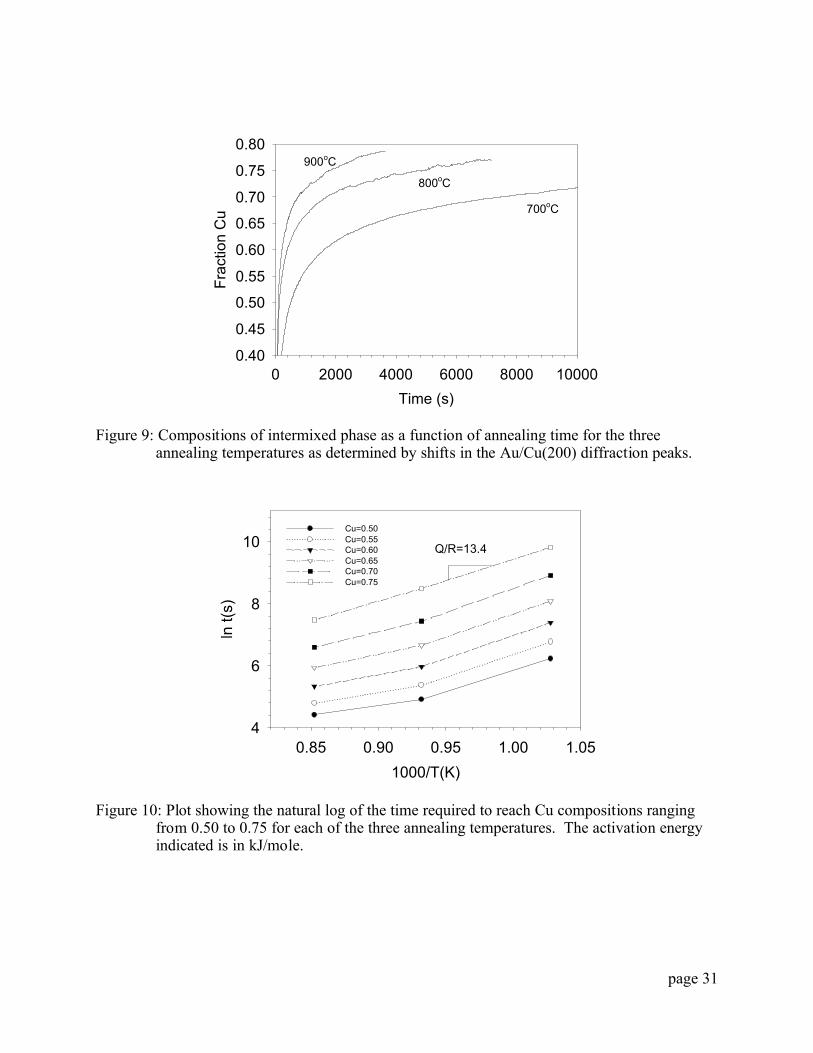
phase based on the fcc (200) diffraction peaks as a function of annealing time. Figure 9 plots the
results for each of the three temperatures up to a total time of 10,000 s, showing the increase in
Cu content with annealing time. As expected, the sample held at 900ºC intermixes more rapidly
page 15
than the samples held at lower temperatures, and all the samples show a decreased rate of
intermixing with increased annealing time. The 700ºC sample was held for a total time longer
than is shown in Fig. 9, eventually reaching a fraction Cu of 0.76 at 28,000 s which is similar to
that observed in the samples held at the higher temperatures for shorter times. At longer times
the Au/Cu diffraction peaks for all three temperatures continue to move to lower d-spacings as
interdiffusion continues.
The time required to reach a given composition of the intermixed phase was determined
from the results presented in Fig. 9 for several different compositions and for each of the three
temperatures using the Au/Cu (200) peaks. These results are presented in Fig. 10, which plots
the natural log time versus 1/T for compositions ranging from 0.5 Cu to 0.75 Cu. As before, the
slope of this line is related to the activation energy for interdiffusion, and it is clear that
activation energies increase with diffusion time. At a Cu fraction of 0.75, the calculated
activation energy is 111.4 kJ/mole, which is nearly twice that of the initial diffusion rate. This
activation energy falls somewhere between grain boundary and bulk diffusion, indicating that the
effects of grain boundaries and defects are decreasing as the interdiffusion becomes more
complete. This effect could be caused by grain growth, which would reduce the amount of grain
boundary area available for diffusion, or by the saturation of grain boundaries and other defects
by interdiffusion.
Note that the diffusion times for the 900ºC temperature at lower amounts of interdiffusion
do not fit the 111.4 kJ/mole trend of the remainder of the data, and appear to require longer times
to reach a given amount of intermixing. This result is most likely due to the partial melting of
the near surface region that occurred in this sample at an early portion of the 900ºC hold. The
partial melting and resolidification increased the grain size of the Au film, thus decreasing the
overall diffusivity in this sample.

page 16
Characterization of the films
Scanning electron microscopy (SEM) was performed on the surface of the films, both
before and after annealing, to determine if the grain boundary structure could be determined.
Figure 11 compares micrographs of the as-received Au surface to those after 700ºC and 900ºC
annealing runs. This surface of the as-deposited Au film (Fig. 11a) has some grooved areas that
are on the order of 10 microns or smaller, which most likely correspond to grain boundaries
carried through the film from the original stainless steel substrate. Within these larger grains,
there are features on the order of 1 micron or smaller which most likely correspond to columnar
grains of the as deposited films which are expected in low temperature deposited thin films [9].
Figure 11b shows the structure of the Au surface after annealing for 8 hours at 700ºC. T size of
the visible surface features appears to be on the order of 2 microns or less, which appears larger
than that of the as deposited film. The sample annealed at 800ºC for 2 hours looked very similar
to the sample held at 700ºC for 8 hours, and is not shown here.
In contrast to the samples annealed at 700ºC and 800ºC, the sample annealed at 900ºC
shows visible grain boundaries with grain sizes in excess of 20 microns. This microstructure is
shown in Fig. 11c, and is pitted with pores up to 1 micron in diameter that are distributed
throughout the grains. In addition, the microstructure shows a lath type substructure throughout
the grains that appear to have a crystallographic orientation relationship to the grains. At 900ºC,
which is near the melting point minimum in the Au-Cu system, diffusion is rapid, allowing the
microstructural changes to rapidly occur. Looking over the individual diffraction patterns for
this run showed that there was a dramatic change in texture when the temperature first reached
its 900ºC set point. Three consecutive diffraction patterns show this transition in Fig. 12. Frame
19 corresponds to a time of 54s after the start of the experiment, just before the sample reaches
page 17
900ºC, while frames 20 and 21 correspond to times of 57s and 60s respectively. Due to thermal
overshoot of the temperature controller, the temperature of the sample spiked to 918ºC in frame
20, before coming back down to 900ºC for the remainder of the experiment. Since the Au/Cu
system has a melting point minimum of 910ºC for a 20wt%Cu composition [10], it is likely that
the sample experienced some degree of melting in the diffuse Au/Cu interface. This melting
would explain the broad diffraction pattern seen in frame 20 and would help to explain the rapid
change in texture of the sample.
A metallographic cross section was made through the sample heated to 800ºC to examine
the microstructure of the Au/Cu intermixed zone after annealing. The SEM micrograph of this
cross section is shown in Fig. 13, indicating that substantial porosity has developed in the near
surface region of the sample. The porosity has a wide size distribution, from less than 100 nm to
500 nm, and appears to be scattered randomly throughout the top 4-5 µm region of the sample.
The origin of this porosity is most likely due to the Kirkedall effect [16] that results from the
different diffusivities of Cu in Au. The different diffusivities causes a net flux of atoms across a
given lattice plane, causing the creation and annihilation of vacancies. Under non-equilibrium
conditions, high vacancy concentrations can be generated and cause the precipitation and growth
of microvoids which eventually create pores of considerable size, such as those indicated in Fig.
13.
In summary, the thin films appear to have initial columnar grain sizes on the order of a
micron or smaller, which results in a high concentration of grain boundaries that accelerate the
diffusion kinetics. These grains appear to coarsen at annealing temperatures of 700ºC and
800ºC, which may contribute to the increased activation energy for diffusion at longer annealing
times. In addition, Kirkendall voids were observed at these annealing temperatures as a result of
the different diffusivities of Au and Cu. At 900ºC, a momentary partial melting of the sample

page 18
created much larger grains and visible voids on the surface of the sample. The larger grains
appear to have slowed the interdiffusion kinetics of this sample relative to what would be
expected if the grain growth had not occurred.
Conclusions
1. In-situ synchrotron radiation was successfully used to track the interdiffusion of Au and Cu
during annealing of thin films at 700ºC to 900ºC. The difference in the lattice parameters of
these two elements allowed the diffraction peaks of each element to be tracked as a function
of annealing time.
2. At short annealing times (<60s) the Cu diffused rapidly through the 3.8µm thick Au film.
This intermixing was characterized by a low d-spacing shoulder which developed on the Au
peak and grew with time. Eventually one diffraction peak was formed as Cu and Au
completely intermixed.
3. The activation energy for interdiffusion was calculated for the initial stage of annealing by
measuring the time required to diffuse Cu through the Au layer of known thickness. This
activation energy was measured to be 65.4 kJ/mole, which is approximately 0.4x that of bulk
diffusion and 0.8x that of grain boundary diffusion values. The low activation energy is
attributed to the high density of columnar grain boundaries combined with other defects in the
thin film microstructure.
4. As interdiffusion proceeds, the Au-rich thin film layer begins to interdiffuse into the Cu layer
below. Homogenization of the two layers takes place over long times and can be tracked as
the Au-rich peak monotonically moves to lower d-spacings for times longer than 60s. The
activation energy for this stage of intermixing was measured to be 111 kJ/mole, which is
between the reported values for grain boundary and bulk diffusion. This change in activation

page 19
energy is believed to be related to grain growth, which would reduce the amount of grain
boundary area available for diffusion, and to the gradual elimination of other defects in the
thin films.
AcknowledgmentsThis work performed under the auspices of the U.S. Department of Energy by UC,
Lawrence Livermore National Laboratory, under Contract No. W-7405-ENG-48. Part of the
research was sponsored by the U.S. Department of Energy Division of Materials Sciences and
Engineering under contract No. DE-AC05-00OR22725 with UT-Battelle, LLC. The UNICAT
facility at the Advanced Photon Source (APS) is supported by the U.S. DOE under Award No.
DEFG02-91ER45439, through the Frederick Seitz Materials Research Laboratory at the
University of Illinois at Urbana-Champaign, the Oak Ridge National Laboratory (U.S. DOE
contract DE-AC05-00OR22725 with UT-Battelle LLC), the National Institute of Standards and
Technology (U.S. Department of Commerce) and UOP LLC. The APS is supported by the U.S.
DOE, Basic Energy Sciences, Office of Science under contract No. W-31-109-ENG-38. The
authors express gratitude to Mr. Ron Forman of LLNL for preparing the PVD coatings, and Mr.
Edwin Sedillo of LLNL for performing scanning electron microscopy.

page 20
References
1. Electronic Materials Handbook, Vol 1, Packaging, edited by L. Abel et al., ASM International, 1989.
2. Th. Heumann and Th. Rottwinkel, Measurement of the Interdiffusion, Intrinsic, and Tracer
Diffusion Coefficients in Cu-Rich Cu-Au Solid Solutions,” J. Nuclear Materials, V69-70, p.
567-570, 1978.
3. F. Hartung and G. Schmitz, “Interdiffusion and reaction of metals: The influence and
relaxation of mismatch-induced stress,” Phys Rev. B, Vol 64(24)/245418(13), 2001.
4. K. N. Tu and B. S. Berry,” X-ray Study of Interdiffusion in Bimetallic Cu-Au Films,” J. Appl. Phys, V 43(8), p. 3283, 1972.
5. J. A. Borders, “Ion Back-Scattering Analysis on Interdiffusion in Cu-Au Thin Films,” Thin Solid Films, V19, pp. 359-370, 1973.
6. A. N. Aleshin, V. K. Egorov, B. S. Bokstein and P. V. Kurkin, “Study of Diffusion in Thin
Au-Cu Films,” Thin Solid Films, V223, pp. 51-55, 1993.
7. T. Surholt and Chr. Herzig, “Grain Boundary Self Diffusion in Cu Polycrystals of Different
Purity,” Acta Mater, V45(9), pp. 3817-3823, 1997.
8. T. Surholt, Yu. M. Mishin, and Chr. Herzog, “Grain-boundary Diffusion and Segregation of
Gold in Copper: Investigation in the type-B and type-C kinetic regime,” Phys Rev B, V50(6),
pp 3577-3587, 1994.
9. Milton Ohring, Materials Science of Thin Films, Deposition and Structure, 2nd ed, Academic
Press, 2002.
10. Binary Alloy Phase Diagrams, Vol 1, 2nd ed, edited by T. B. Massalski, ASM International, 1990.
11. J. W. Elmer, J. Klingmann, and K. Van Bibber, “Diffusion Bonding and Brazing of High
Purity Copper for the Next Linear Collider,” Physical Review Special Topics—Accelerators and Beams, Vol. 4, Issue 5, APS, 53502-1 to16, 2001.
12. J. W. Elmer, T. A. Palmer, S. S. Babu and E. D. Specht,”Low Temperature Relaxation of
Residual Stress in Ti-6Al-4V,” Scripta Materialia, v52, pp1051-1056, 2005.
13. J. W. Elmer, T. A. Palmer, S. S. Babu, and E. D. Specht, "In-situ Observations of Lattice
Expansion and Transformation Rates of α and β Phases in Ti-6Al-4V," Materials Science
and Engineering A, 391, pp104-113, January, 2005.

page 21
14. A. P. Hammersley, FIT2D V9.129 Reference Manual V3.1, ESRF Internal Report,
ESRF98HA01T, 1998.
15. A.P. Hammersley, S.O. Svensson, M. Hanfland, A.N. Fitch, D. Häusermann, High Pressure Research, 14, 235-248, 1998.
16. B. D. Cullity and S. R. Stock, Elements of X-Ray Diffraction, 3rd Ed, Prentice Hall, Upper
Saddle River, NJ, 2001.
17. C. J. Smithells, E. A. Brandes, G. B. Brook. Smithells Metal Reference Book, 7th ed,
Butterworth-Heinemann Ltd., Oxford, United Kingdom, 1992.
18. P. D. Shewmon, Diffusion in Solids, McGraw Hill, 1963.
19. J. W. Christian: The Theory of Transformations in Metals and Alloys, 2nd Edition, Part I,1975, Oxford: Pergamon.
20. C. S. Barrett, Structure of Metals, McGraw Hill, 1943.

page 22
Table 1: Estimated diffusion coefficients for the three temperatures based on the peak width
measurements.
Time to diffuse
through Au layer
(s)
Temperature
(ºC)
Au-film thickness
(µm)
D
(µm2/s)
54 700 3.38 0.053
38 800 3.76 0.093
22 900 4.33 0.213

page 23
Figure Captions
Figure 1: a) Schematic of the x-ray setup used for in-situ observations of phase transformations under controlled heating and cooling conditions. b) Photograph of the center section of one of the coated samples, showing the Au layer (25 mm wide) on top of the Cu layer and stainless steel substrate.
Figure 2: Initial diffraction pattern of the gold-coated copper sample at room temperature, showing Deby arcs on the CCD areal detector. The Bragg angle is highest, the d-spacing lowest, and the top of the pattern.
Figure 3: Initial diffraction pattern at room temperature showing 3 sets of diffraction peaks for each of the Au and Cu layers. An additional Au peak appears at the lowest d-spacing.
Figure 4: D-spacings (symbols) for the Au 200 and Cu 200 planes as a function of time for: a) 700 ºC, b) 800 ºC, and c) 900 ºC. The solid lines plot the temperature profile of the sample.
Figure 5: Comparison between the initial and the final diffraction pattern of the sample held at 800°C for 2 hrs. The initial Cu peaks disappear, while the lattice parameter of the Au peaks decrease as indicated by the arrows. Similar changes were observed in the samples held at 700°C and 900°C.
Figure 6: Peak profiles for the (220) reflections taken at 3-s intervals during the 800°C anneal. These profiles show the rapid interdiffusion stage from t=36s to t=57s, where a Cu-rich shoulder builds up and grows on the low d-spacing side of the Au peak, and eventually creates a single Au/Cu peak.
Figure 7: Peak widths versus time for each of the three annealing temperatures. Narrowing of the peaks occurs around t=20s due to annealing. The spike in peak widths corresponds to diffusion of Cu into the Au layer.
Figure 8: Comparison of the initial thin-film diffusion coefficient with reported bulk diffusion values for Au in Cu and Cu in Au (dashed lines). The results of this study (solid line and symbols) for thin films based on the spike in peak widths at early annealing times. Activation energies are in KJ/mole.
Figure 9: Compositions of intermixed phase as a function of annealing time for the three annealing temperatures as determined by shifts in the fcc(200) diffraction peaks.
Figure 10: Plot showing the natural log of the time required to reach Cu compositions ranging from 0.50 to 0.75 for each of the three annealing temperatures. The activation energy indicated is in kJ/mole.
Figure 11: Scanning electron micrographs of the Au surface. A) Prior to annealing, B) after annealing at 700ºC, and 800ºC) after annealing at 900ºC.
Figure 12: Three consecutive x-ray diffraction peaks from the sample heated to 900ºC. These x-

page 24
ray patterns show the change in texture from Au(111) to Au(200), and a shift to lower d-spacing as Cu diffuses into the Au layer.
Figure 13: SEM cross section micrograph of the near surface region of the sample annealed at 700ºC. Kirkendall voids appear in a zone of thickness similar to that of the initial Au layer.

page 25
a)
25 mmb)
Figure 1: a) Schematic of the x-ray setup used for in-situ observations of phase transformations under controlled heating and cooling conditions. b) Photograph of the center section of one of the coated samples, showing the Au layer (25 mm wide) on top of the Cu layer and stainless steel substrate.

page 26
Figure 2: Initial diffraction pattern of the gold-coated copper sample at room temperature, showing Deby arcs on the CCD areal detector. The Bragg angle is highest and the d-spacing lowest at the top of the pattern.
d-spacing( Å )
1.2 1.4 1.6 1.8 2.0 2.2 2.4
Rel
ativ
e In
tens
ity
0.00
0.01
0.02
0.03
0.04
0.05Au(111)
Cu(111)
Au(200)
Cu(200)
Au(220)
Cu(220)
Au(311)
Figure 3: Initial diffraction pattern at room temperature showing 3 sets of diffraction peaks for each of the Au and Cu layers. An additional Au peak appears at the lowest d-spacing.

page 27
Time (s)
0 50 100 150 200
d-sp
acin
g (Å
)
1.80
1.85
1.90
1.95
2.00
2.05
2.10
Tem
pera
ture
(ºC
)
0
200
400
600
800
1000
Cu 200
Au 200
Temperature
a
Time (s)
0 50 100 150 200
d-sp
acin
g (Å
)
1.80
1.85
1.90
1.95
2.00
2.05
2.10
Tem
pera
ture
(ºC
)0
200
400
600
800
1000
Cu 200
Au 200
Temperature
b
Time (s)
0 50 100 150 200
d-sp
acin
g (Å
)
1.80
1.85
1.90
1.95
2.00
2.05
2.10
Tem
pera
ture
(ºC
)
0
200
400
600
800
1000
Cu 200
Au 200
Temperature
c
Figure 4: D-spacings (symbols) for the Au 200 and Cu 200 planes as a function of time for: a) 700 ºC, b) 800 ºC, and c) 900 ºC. The solid lines plot the temperature profile of the sample.

page 28
d-spacing (Å)
1.2 1.4 1.6 1.8 2.0 2.2 2.4
Inte
nsity
0.00
0.02
0.04
0.06
0.08
0.10800ºC Au(111)
Au(200)
Au(220)
Figure 5: Comparison between the initial and the final diffraction pattern of the sample held at 800°C for 2 hrs. The initial Cu peaks disappear, while the lattice parameter of the Au peaks decrease as indicated by the arrows. Similar changes were observed in the samples held at 700°C and 900°C.
d-spacing (Å)
1.25 1.30 1.35 1.40 1.45 1.50
Inte
nsity
0.000
0.002
0.004
0.006
0.008
0.010
0.012800ºC
Cu(220) Au(220)
t=36s
t=57s
Figure 6: Peak profiles for the (220) reflections taken at 3-s intervals during the 800°C anneal. These profiles show the rapid interdiffusion stage from t=36s to t=57s, where a Cu-rich shoulder builds up and grows on the low d-spacing side of the Au peak, and eventually creates a single Au/Cu peak.

page 29
Time (s)0 20 40 60 80 100 120
Pea
k W
idth
(Å)
0.006
0.007
0.008
0.009
0.010
0.011700oC
800oC900oC
Figure 7: Peak widths versus time for each of the three annealing temperatures. Narrowing of the peaks occurs around t=20s due to annealing. The spike in peak widths corresponds to diffusion of Cu into the Au layer.
1000/T(K)0.80 0.85 0.90 0.95 1.00 1.05
ln D
(µm
2 /s)
-6
-5
-4
-3
-2
-1
-Q/R=7.87
Cu in AuAu in Cu
Thin Film
-Q/R=23.8-Q/R=20.4
Figure 8: Comparison of the initial thin-film diffusion coefficient with reported bulk diffusionvalues for Au in Cu and Cu in Au (dashed lines). The results of this study (solid line and symbols) for thin films based on the spike in peak widths at early annealing times. Activation energies are in KJ/mole.

page 30
page 31
Time (s)0 2000 4000 6000 8000 10000
Frac
tion
Cu
0.40
0.45
0.50
0.55
0.60
0.65
0.70
0.75
0.80
700oC
800oC
900oC
Figure 9: Compositions of intermixed phase as a function of annealing time for the three annealing temperatures as determined by shifts in the Au/Cu(200) diffraction peaks.
1000/T(K)0.85 0.90 0.95 1.00 1.05
ln t(
s)
4
6
8
10Cu=0.50Cu=0.55Cu=0.60Cu=0.65Cu=0.70Cu=0.75
Q/R=13.4
Figure 10: Plot showing the natural log of the time required to reach Cu compositions ranging from 0.50 to 0.75 for each of the three annealing temperatures. The activation energy indicated is in kJ/mole.

page 32
10 mµa
10 mµb
10 mµc
Figure 11: Scanning electron micrographs of the Au surface. A) Prior to annealing, B) after annealing at 700ºC, and C) after annealing at 900ºC.

page 33
d-spacing (A)1.2 1.4 1.6 1.8 2.0 2.2 2.4
Inte
nsity
0.0
0.2
0.4
0.6
0.8
1.0
frame 19frame 20frame 21
Au(111)
Au(200)
Au(220)
Figure 12: Three consecutive x-ray diffraction peaks from the sample heated to 900ºC. These x-ray patterns show the change in texture from Au(111) to Au(200), and a shift to lower d-spacing as Cu diffuses into the Au layer.
2 mµ
Figure 13: SEM cross section micrograph of the near surface region of the sample annealed at 700ºC. Kirkendall voids appear in a zone of thickness similar to that of the initial Au layer.
Recommended