8/14/2019 Effects of the Thickness of GaAs Spacer Layers on the Structure of Multi Layer
http://slidepdf.com/reader/full/effects-of-the-thickness-of-gaas-spacer-layers-on-the-structure-of-multi-layer 1/5
Effects of the thickness of GaAs spacer layers on the structure of multilayer
stacked InAs quantum dots
Hyung Seok Kim a, Ju Hyung Suh a, Chan Gyung Park a,Ã, Sang Jun Lee b, Sam Kyu Noh b, Jin Dong Song c,Yong Ju Park c, Won Jun Choi c, Jung Il Lee c
a Department of Materials Science and Engineering, Pohang University of Science and Technology (POSTECH), Pohang, Kyungbuk 790-784, Republic of Koreab Quantum Dot Technology Laboratory, Korea Research Institute of Standards and Science (KRISS), Daejeon 305-600, Republic of Koreac Nano Device Research Center, Korea Institute of Science and Technology (KIST), Seoul 136-791, Republic of Korea
a r t i c l e i n f o
Article history:
Received 13 September 2005
Received in revised form
13 October 2008
Accepted 20 October 2008
Communicated by K.H. PloogAvailable online 1 November 2008
PACS:
68.37.Lp
68.43.Hn
68.55.Jk
68.65.Hb
Keywords:
A1. Microstructure characterizationA1. Quantum dots
A1. Transmission electron microscopy
(TEM)
B1. Multilayer InAs/GaAs
a b s t r a c t
The effects of the thickness of GaAs spacer layers on the structure of multilayer stacked InAs quantum
dots (QDs) grown by molecular-beam epitaxy were studied using transmission electron microscopy. To
investigate QD structure depending on spacer layer growth, first uncapped free-standing QDs were
grown and their structure compared with that of multilayer stacked QDs. In addition, vertically
nonaligned and aligned stacked QDs were grown by adjusting the thickness of GaAs spacer layers. The
uncapped QDs were found to form a lens-shaped structure with side facets. Upon capping with a GaAs
spacer, the apex of nonaligned QDs flattened by In diffusion. However, the aligned QDs maintained their
lens-shaped structure with round apex after capping. It is believed that their apex did not flatten
because the chemical potential gradient of In was relatively low due to the adjacent InAs QD layers. The
results demonstrate the possibility of controlling QD structure by adjusting the thickness of spacer
layers.
& 2008 Published by Elsevier B.V.
1. Introduction
Recently self-assembled heteroepitaxial quantum dots (QDs)
have been grown in Stranski-Krastanow mode [1] and consider-
able effort has been devoted to fabricating laser devices [2],
photodetectors [3] and advanced memory [4] by using self-
assembled QDs. To understand and control the optoelectronic
properties of QD devices, the shape and size of QDs have to bemeasured exactly because their optoelectronic properties are
significantly dependent on their structural properties such as
shape, size, uniformity and density. In addition, the study of the
detailed structure of QDs provides new insight into understanding
the growth characteristics of QDs and controlling their growth
parameters.
There are many important growth parameters such as growth
temperature, deposition rate, growth interruption and the growth
condition of cap layers, which affect the QD structures and their
optoelectronic properties. In particular, the growth procedure of a
cap layer plays a crucial role in determining QD structure and
various QD shapes, depending on cap layer growth have been
reported including truncation [5], ride-valley transition [6] and
dissolution of QDs [7]. Typical analysis of the effect of cap layer
growth on the QD structure was performed using atomic force
microscopy (AFM) in uncapped or partially capped QDs andshowed an important material redistribution during cap layer
growth [8,9]. However, the AFM investigation is not capable of
resolving QD structure owing to the well-known tip convolution
effect, and it is impossible to investigate the structure of fully
capped QDs. Transmission electron microscopy (TEM) is a unique
analysis technique for investigating QD structures capped with an
overlayer and atomic scale analyses are also possible by high-
resolution electron microscopy (HREM).
In the present study, multilayer stacked InAs QDs were grown
on GaAs by molecular-beam epitaxy (MBE) and their structural
properties were investigated by field emission gun-TEM (FEG-TEM)
and high-voltage electron microscopy (HVEM) depending on the
thickness of spacer cap layers. The uncapped QDs were found to
ARTICLE IN PRESS
Contents lists available at ScienceDirect
journal homepage: www.elsevier.com/locate/jcrysgro
Journal of Crystal Growth
0022-0248/$- see front matter & 2008 Published by Elsevier B.V.doi:10.1016/j.jcrysgro.2008.10.054
ÃCorresponding author. Tel.: +8254 2792139; fax: +8254 2792399.
E-mail addresses: [email protected] (H.S. Kim).
[email protected] (C.G. Park).
Journal of Crystal Growth 311 (2009) 258–262

8/14/2019 Effects of the Thickness of GaAs Spacer Layers on the Structure of Multi Layer
http://slidepdf.com/reader/full/effects-of-the-thickness-of-gaas-spacer-layers-on-the-structure-of-multi-layer 2/5
form a lens-shaped structure with side facets. In addition,
vertically nonaligned and aligned stacked QDs were grown by
adjusting the thickness of GaAs spacer layers. Upon capping by
GaAs, the apex of nonaligned QDs flattened by In diffusion
although the aligned QDs maintained their lens-shaped structure
with round apex.
2. Experimental procedure
The InAs QDs were grown on semi-insulating GaAs(0 0 1)
substrates using the MBE system (RIBER32P). In order to
investigate the effects of GaAs spacer growth on the QD structure,
uncapped QDs were grown and their structures were investigated
by AFM and HREM. In addition, two different samples, one
vertically aligned and the other nonaligned along the growth
direction, were grown by varying the thickness of GaAs spacer
layers. Fig. 1 shows the schematic diagram of five-period stacked
InAs/GaAs QDs heterostructures. The GaAs buffer layer with a
thickness of 250 nm was deposited on the substrate at 5601C. The
InAs QDs with an equivalent thickness of 2.5 monolayers (ML)
were formed and GaAs overlayers were deposited at 4801C. Forthe growth of vertically nonaligned and aligned QDs, 49 and 9 nm
thick GaAs spacers were deposited, respectively. The growth of
InAs QDs and GaAs spacers was repeated five times with growth
rates of 1.4 and 12.4 nm/min, respectively.
The structural properties of QDs were studied using AFM
(Dimension 3100, Digital Instruments) in tapping mode and
200 kV HR-TEM (JEM-2010F, JEOL). In addition, scanning-TEM
(STEM; JEM2100F, JEOL) with energy dispersive X-ray spectro-
scopy (EDS) and 1.25 MV HVEM (JEM-ARM1300S, JEOL) located
at the Korea Basic Science Institute (KBSI) were used for the
observation of QD structures on an atomic-length scale. TEM
investigations were performed by conventional bright field (BF)
TEM and HREM techniques. TEM images were recorded on an
image plate and their resolution was improved enough to measure
QD size using digital intensity profiling through fast Fourier
transformation (FFT) and the inverse FFT processes.
3. Results and discussion
Fig. 2(a) shows an AFM height image of uncapped InAs QDs
measured in tapping mode. The QDs were lens-shaped and their
average height and diameter were 3.5 and 35 nm, respectively.
The QDs were distributed randomly and had a tendency to grow
together in twos or threes. The QDs density was 7.7Â1010cmÀ2.
Fig. 2(b) is an AFM height profile of single QD indicated in the
Fig. 2(a) by the dotted line A–B. The section profile shows that the
QD has symmetrical dimensions and QD height and diameter
were measured as 3.75 and 36 nm, hence the aspect ratio was
about 0.1.
However, the cross-sectional HREM of uncapped QDs revealedthat the lateral dimension measured by AFM was enlarged by
about two times although the QDs height by AFM nearly coincided
with the result by TEM. Fig. 2(c) shows the HREM image of
uncapped QD on [110] zone. The QD height and the diameter
of base were measured as $4.2 and $18.5nm, respectively, and
hence the aspect ratio was 0.23 which is more than twice as large
as the result by AFM. The resolution of AFM is limited by the
sharpness and shape of the tip whose normal radius of curvature
is 20–60nm [10]. In particular, lateral resolution is much more
dependent on the dimension of the tip than vertical resolution in
nanometer-sized samples because of the measuring geometry
between the tip and sample [11]. Considering the QD structure by
TEM, it is believed that the lateral dimension of QDs measured by
AFM is not reliable although their vertical dimension by AFM isreasonable. The HREM also shows that the QDs are coherent
islands without any defects such as dislocations or stacking faults.
The uncapped QDs were lens-shaped with side facets whose
wetting angles were about 261. The phenomenon of equilibrium
faceting plays a crucial role in determining the QD shape [12]. The
facets with high Miller indices such as (136), (137), (125) and
(2511) were reported in many studies using scanning tunneling
microscopy, AFM and reflection high-energy electron diffraction.
The facet angle was measured as 23–281 and the main facet angle
was 261 which coincides with the (137) facet [12].
We have investigated the structure of uncapped InAs QDs
before GaAs spacer growth. However, the QDs have to be covered
with a cap layer which is needed for the passivation of the QDs
for device application. In addition, multilayer stacked QDs are
required to increase the QD density and the optoelectronic
efficiency of QD devices [13]. In the present study, therefore,
five-period stacked QD structures were grown with varying the
thickness of spacer layers, after which the effects of GaAs spacer
overlayer on the QD structures were investigated.
Fig. 3 shows a cross-sectional TEM BF image of five-period
stacked InAs QDs with 49 nm thick GaAs spacer layers and the
[110] zone HREM image (b). The five-period stacked QDs were
successively grown and randomly distributed along the growth
direction. A lens-shaped very dark contrast was observed on and
beneath the wetting layers under the g 004 two beam condition.
The InAs/GaAs heteroepitaxy has a 7.2% lattice misfit and the
misfit strain induces a dark contrast in TEM observations using
phase contrast as well as diffraction contrast. The QD height and
diameter were measured as 3.5–4.5 and 15–20 nm, respectively.In particular, the BF and HREM images show that QD apexes
flattened after capping with a spacer layer. The effects of elastic
energy and surface energy can explain the QD apex flattening
[6,14]. The increase of the elastic energy and surface energy of
InAs QDs by depositing a GaAs overlayer induces the diffusion of
In from the QDs [14]. Therefore, QD apex flattening is possible due
to the In diffusion induced by the compressive strain from GaAs to
QDs and the chemical potential gradient of In during overlayer
growth at high temperature. The QD height and base diameter
were measured as $4.6 and $23.2nm in the HREM. However,
exact determination of the shape and size of capped QDs was
difficult because of the indistinct boundary between InAs and
GaAs as shown in Fig. 3(b). In the BF image under dynamical two
beam and the HREM on-zone axis multi beam conditions, thediffraction contrast image of QDs can be observed largely by strain
ARTICLE IN PRESS
Fig. 1. Schematic diagram of five-period stacked InAs QDs grown on GaAs.
H.S. Kim et al. / Journal of Crystal Growth 311 (2009) 258–262 259

8/14/2019 Effects of the Thickness of GaAs Spacer Layers on the Structure of Multi Layer
http://slidepdf.com/reader/full/effects-of-the-thickness-of-gaas-spacer-layers-on-the-structure-of-multi-layer 3/5
ARTICLE IN PRESS
Fig. 2. AFM height image of a free-standing uncapped InAs QDs in tapping mode (a), section height profile indicated by dotted line A–B in (a), and a [110] zone cross-
sectional HREM image of a single QD showing lens-shaped structure.
Fig. 3. Cross-sectional BF image of five-period stacked InAs QDs with 49 nm thick GaAs spacers in g 004 two beam condition (a) and the [110] HREM image of the QD
showing flat QD apex (b).
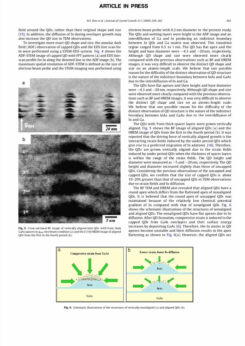
Fig. 4. Annular dark field (ADF) STEM image of capped QD with FFT pattern (a) and EDS line-scan profile for In along the denoted line in the ADF image (b).
H.S. Kim et al. / Journal of Crystal Growth 311 (2009) 258–262260
8/14/2019 Effects of the Thickness of GaAs Spacer Layers on the Structure of Multi Layer
http://slidepdf.com/reader/full/effects-of-the-thickness-of-gaas-spacer-layers-on-the-structure-of-multi-layer 4/5
field around the QDs, rather than their original shape and size
[15]. In addition, the diffusion of In during overlayer growth may
also increase the QD size in TEM observations.
To investigate more exact QD shape and size, the annular dark
field (ADF) observation of capped QDs and the EDS line scan for
In were performed using a STEM-EDS system. Fig. 4 shows the
ADF-STEM image of capped QD with FFT pattern (a) and EDS line-
scan profile for In along the denoted line in the ADF image (b). Themaximum spatial resolution of ADF-STEM is defined as the size of
electron beam probe and the STEM imaging was performed using
electron beam probe with 0.2 nm diameter in the present study.
The QDs and wetting layers were bright in the ADF image and an
interdiffusion of Ga and In producing an indistinct boundary
between In QDs and Ga matrix was observed. This transition
region ranged from 0.5 to 1 nm. The QD has flat apex and the
height and base diameter were $4.3 and $20 nm, respectively.
Although QD shape and size were observed more clearly
compared with the previous observations such as BF and HREMimages, it was very difficult to observe the distinct QD shape and
size on an atomic-length scale. We believe that one possible
reason for the difficulty of the distinct observation of QD structure
is the nature of the indistinct boundary between InAs and GaAs
due to the interdiffusion of In and Ga.
The QDs have flat apexes and their height and base diameter
were $4.3 and $20 nm, respectively. Although QD shape and size
were observed more clearly compared with the previous observa-
tions such as BF and HREM images, it was very difficult to observe
the distinct QD shape and size on an atomic-length scale.
We believe that one possible reason for the difficulty of the
distinct observation of QD structure is the nature of the indistinct
boundary between InAs and GaAs due to the interdiffusion of
In and Ga.The QDs with 9 nm thick spacer layers were grown vertically
aligned. Fig. 5 shows the BF image of aligned QDs (a) and the
HREM image of QDs from the first to the fourth period (b). It was
reported that the driving force of vertically aligned growth is the
interacting strain fields induced by the under period QDs which
give rise to a preferred migration of In adatoms [16]. Therefore,
the QDs are grown vertically aligned due to the strain fields
induced by under period QDs when the thickness of spacer layers
is within the range of the strain fields. The QD height and
diameter were measured as $5 and $20 nm, respectively. The QD
height and diameter increased slightly than those of uncapped
QDs. Considering the previous observations of the uncapped and
capped QDs, we confirm that the size of capped QDs is about
10–20% greater than that of uncapped QDs in TEM observations
due to strain fields and In diffusion.
The BF TEM and HREM also revealed that aligned QDs have a
round apex which differs from the flattened apex of nonaligned
QDs. It is believed that the round apex of uncapped QDs was
maintained because of the relatively low chemical potential
gradient of In compared with that of nonaligned QDs. Fig. 6
shows the schematic illustrations of the structures of nonaligned
and aligned QDs. The nonaligned QDs have flat apexes due to In
diffusion. After QD formation, compressive strain is induced to the
capped QDs from GaAs overlayers and their surface energy
increases by depositing GaAs [6]. Therefore, the In atoms in QD
apexes become unstable and their diffusion results in the apex
flattening as shown in Fig. 6(a). However, the aligned QDs are
ARTICLE IN PRESS
Fig. 5. Cross-sectional BF image of vertically aligned InAs QDs with 9 nm thick
GaAs spacers in g 004 two beam condition (a) and the [110] HREM image of aligned
QDs from the first to the fourth period (b).
Fig. 6. Schematic illustrations of the structures of vertically nonaligned (a) and aligned QDs (b).
H.S. Kim et al. / Journal of Crystal Growth 311 (2009) 258–262 261

8/14/2019 Effects of the Thickness of GaAs Spacer Layers on the Structure of Multi Layer
http://slidepdf.com/reader/full/effects-of-the-thickness-of-gaas-spacer-layers-on-the-structure-of-multi-layer 5/5
more stable than the nonaligned QDs because the strain fields
caused by under period QDs reduce the misfit strain between InAs
and GaAs. It has been demonstrated that the compressive strain
in aligned QDs is significantly lower than that in single-layer or
nonaligned QDs [17]. In addition, it is confirmed that the chemical
potential gradient of In is relatively low due to the adjacent InAs
layers. Therefore, the nonaligned QDs flattened but the aligned
QDs did not flatten after spacer layer growth.
4. Conclusion
Vertically nonaligned and aligned InAs QDs were grown by
adjusting the thickness of GaAs spacer layers. The apexes of
nonaligned QDs were flattened by In diffusion after capping with a
spacer layer, although the uncapped QDs were lens-shaped
structures with round apexes. However, the aligned QDs main-
tained their lens-shaped structure after capping. Efficient adjust-
ing of the thickness of spacer layers may be a crucial factor for
controlling the structure of multilayer stacked QDs.
Acknowledgements
This work was supported in part by the Ministry of Science and
Technology through the National Research Laboratory on Quan-
tum-dot Technology at the Korea Research Institute of Standards
and Science (M1-0104-00-0127). The work in KIST was supported
in part by Nano R&D project by MOCIE ROK and QC project by
MOST ROK. One of authors (S.K. Noh) acknowledges the partial
support provided by the Korea Science and Engineering Founda-
tion through the Quantum-functional Semiconductor Research
Center at Dongguk University.
References
[1] D.J. Eaglesham, Phys. Rev. Lett. 64 (1990) 1943.
[2] I.N. Kaiander, R.L. Sellin, T. Kettler, N.N. Ledentsov, D. Bimberg, N.D. Zakharov,P. Werner, Appl. Phys. Lett. 84 (2004) 2992.[3] J. Phillips, K. Kamath, P. Bhattacharya, Appl. Phys. Lett. 72 (1998) 2020.[4] K. Yano, T. Ishii, T. Hashimoto, T. Kobayashi, F. Murai, K. Seki, IEEE Trans.
Electron Devices 41 (1994) 1628.[5] V. Tokranov, M. Yakimov, A. Katsnelson, M. Lamberti, S. Oktyabrsky, Appl.
Phys. Lett. 83 (2003) 833.[6] R. Songmuang, S. Kiravittaya, O.G. Schmidt, J. Crystal Growth 249 (2003) 416.[7] A. Lenz, H. Eisele, R. Timm, S.K. Becker, R.L. Sellin, U.W. Pohl, D. Bimberg,
M. Dahne, Appl. Phys. Lett. 84 (2004) 2992.[8] N.P. Kobayashi, T.R. Ramachandran, P. Chen, A. Madhukar, Appl. Phys. Lett. 68
(1996) 3299.[9] B. Basnar, H. Hiener, E. Gornic, G. Strasser, J. Crystal Growth 264 (2004) 26.
[10] Q. Gong, J.B. Liang, B. Xu, D. Ding, H.X. Li, C. Jiang, W. Zhou, F.Q. Liu, Z.G. Wang,X.H. Qiu, G.Y. Shang, C.L. Bai, J. Crystal Growth 192 (1998) 376.
[11] Shen-De Chen, Chiou-Yun Tsai, Si-Chen Lee, J. Nanopart. Res. 6 (2004) 407.[12] K. Jacobi, Prog. Surf. Sci. 71 (2003) 185.[13] H. Heidemeyer, S. Kiravittaya, C. Muller, N.Y. Jin-Phillipp, Appl. Phys. Lett. 80
(2002) 1544.
[14] N.N. Ledentsov, V.A. Shchukin, M. Grundmann, N. Kirstaedter, J. Bohrer,O. Schmidt, D. Bimberg, V.M. Ustinov, A.Y. Egorov, A.E. Zhukov, P.S. Kop’ev,S.V. Zaitsev, N.Y. Gordeev, Z.I. Alferov, A.I. Borovkov, A.O. Kosogov,S.S. Ruvimov, P. Werner, U. Gosele, J. Heydenreich, Phys. Rev. B 54 (1996)8743.
[15] X.G. Liao, J. Zou, X.F. Duan, D.J.H. Cockayne, R. Leon, C. Lobo, Phys. Rev. B 58(1998) R4235.
[16] Quianghua Xie, Anupam Madhukar, Ping Chen, Nobuhiko P. Kobayashi, Phys.Rev. Lett. 75 (1995) 2542.
[17] N.Y. Jin-Phillipp, F. Phillipp, J. Appl. Phys. 88 (2000) 710.
ARTICLE IN PRESS
H.S. Kim et al. / Journal of Crystal Growth 311 (2009) 258–262262
Recommended