ESE 570: Digital Integrated Circuits and VLSI Fundamentals
Lec 16: March 21, 2017 Transmission Gates, Euler Paths, Energy
Basics Review
Penn ESE 570 Spring 2017 – Khanna

Midterm
! Midterm " Mean: 79.5 " Standard Dev: 14.5
2 Penn ESE 570 Spring 2017 – Khanna

Lecture Outline
! Pass Transistor Logic ! Euler Path for Layout ! Energy and Power Basics ! Energy and Power Optimization
3 Penn ESE 570 Spring 2017 – Khanna

Pass Transistor Logic
Penn ESE 570 Spring 2017 – Khanna

Output
! What is Vout if A=0, B=0? if A=1, B=0?
5
A B Y
0 0 0
0 1 1
1 0 1
1 1 0
Penn ESE 570 Spring 2017 – Khanna

Restore Output
6 Penn ESE 570 Spring 2017 – Khanna

Chain Together
7 Penn ESE 570 Spring 2017 – Khanna

Analyze Stage
8 Penn ESE 570 Spring 2017 – Khanna

Delay A=1, B=1, Cdiff≠0? (W=1)
9 Penn ESE 570 Spring 2017 – Khanna

10
! What’s the equivalent RC circuit?
Delay A=1, B=1, Cdiff≠0? (W=1)
Penn ESE 570 Spring 2017 – Khanna

Transmission Gates
Penn ESE 570 Spring 2017 – Khanna

CMOS Transmission Gates
12
Kenneth R. Laker, University of Pennsylvania,
updated 26Feb15
Penn ESE 570 Spring 2017 – Khanna

CMOS Transmission Gates
13
Kenneth R. Laker, University of Pennsylvania,
updated 26Feb15
at t = 0-: Vin = 0, Vout = 0 at t = 0+: Vin = 0 -> VDD
Note
Penn ESE 570 Spring 2017 – Khanna

CMOS Transmission Gates
14
Kenneth R. Laker, University of Pennsylvania,
updated 26Feb15
at t = 0-: Vin = 0, Vout = 0 at t = 0+: Vin = 0 -> VDD
Note
- VTp
≥ ≥
≤
Penn ESE 570 Spring 2017 – Khanna

CMOS Transmission Gates
15
Kenneth R. Laker, University of Pennsylvania,
updated 26Feb15
at t = 0-: Vin = 0, Vout = 0 at t = 0+: Vin = 0 -> VDD
Note
- VTp
≥ ≥
≤
Penn ESE 570 Spring 2017 – Khanna

CMOS Transmission Gates
16
Kenneth R. Laker, University of Pennsylvania,
updated 26Feb15
at t = 0-: Vin = 0, Vout = 0 at t = 0+: Vin = 0 -> VDD
Note
- VTp
≥ ≥
≤
Penn ESE 570 Spring 2017 – Khanna

CMOS Transmission Gates
17 - VTp
≥ ≥
≤
Penn ESE 570 Spring 2017 – Khanna

Transmission Gate, Req
18
kp (- VDD - VTp)2
kp [2(- VDD - Vtp) (Vout – VDD) - (Vout – VDD)2]
kp [2(- VDD - Vtp) - (Vout – VDD)]
kp [2(- VDD - Vtp) (Vout – VDD) - (Vout – VDD)2]
kp [2(- VDD - Vtp) - (Vout – VDD)]
Penn ESE 570 Spring 2017 – Khanna

19
Kenneth R. Laker, University of Pennsylvania,
updated 26Feb15
Transmission Gate, Req
Penn ESE 570 Spring 2017 – Khanna

20
Kenneth R. Laker, University of Pennsylvania,
updated 26Feb15
Transmission Gate, Req
Penn ESE 570 Spring 2017 – Khanna

Transmission Gate Layouts
21
Kenneth R. Laker, University of Pennsylvania,
updated 26Feb15
Penn ESE 570 Spring 2017 – Khanna

Performance Design
Penn ESE 570 Spring 2017 – Khanna

NOR2 Layout
23
Kenneth R. Laker, University of Pennsylvania,
updated 26Feb15
Penn ESE 570 Spring 2017 – Khanna

NAND2 Layout
24 Penn ESE 570 Spring 2017 – Khanna

Layout of Complex CMOS Gate
25
Kenneth R. Laker, University of Pennsylvania,
updated 26Feb15
DS DSGND
Penn ESE 570 Spring 2017 – Khanna

Layout of Complex CMOS Gate
26
Kenneth R. Laker, University of Pennsylvania,
updated 26Feb15
Penn ESE 570 Spring 2017 – Khanna

27
Kenneth R. Laker, University of Pennsylvania,
updated 26Feb15
d
d d
d
d
i.e. n, p Euler paths with identical sequences of inputs
.
diffusion breaks
Layout of Complex CMOS Gate
Penn ESE 570 Spring 2017 – Khanna

Minimize Number of Diffusion Paths
28
Kenneth R. Laker, University of Pennsylvania,
updated 26Feb15
Penn ESE 570 Spring 2017 – Khanna

Minimize Number of Diffusion Paths
29
Kenneth R. Laker, University of Pennsylvania,
updated 26Feb15
Penn ESE 570 Spring 2017 – Khanna

Minimize Number of Diffusion Paths
30
Kenneth R. Laker, University of Pennsylvania,
updated 26Feb15
Penn ESE 570 Spring 2017 – Khanna

Minimize Number of Diffusion Paths
31
Kenneth R. Laker, University of Pennsylvania,
updated 26Feb15
Penn ESE 570 Spring 2017 – Khanna

Gate Layout Algorithm
! 1. Find all Euler paths that cover the graph ! 2. Find common n- and p- Euler paths ! 3. If no common n- and p- Euler paths are found in
step 2, partition the gate n- and p- graphs into the minimum number of sub-graphs that will result in separate common n- and p- Euler paths
32
Kenneth R. Laker, University of Pennsylvania,
updated 26Feb15
Penn ESE 570 Spring 2017 – Khanna

Review
Motivation, Abstraction, and Design Tradeoffs
Penn ESE 570 Spring 2017 – Khanna

Digital Logic: Gate Level
! We care about design for performance " Functionality (e.g. F = A + B*C) " Speed
" Each gate has a delay caused by the output resistance and capacitive load (which is the input capacitive load of the gate on the output)
" Critical path defines delay
" Power " Switching power (comprised of dynamic and short circuit power) and
static power (I.e Ptot=Pdyn+PSC+ Pstat)
" Area " For a gate the standard cell area, dependent on W and L of transistors
34 Penn ESE 570 Spring 2017 – Khanna

Digital Logic: Transistor Level
35 Penn ESE 570 Spring 2017 – Khanna

Digital Logic: Transistor Level
! We care about design for performance " Functionality (e.g. F = A + B*C)
" Design for abstraction (VTC: switching voltage, high gain, noise margins)
" Speed " Transistor sizing affects the output resistance and capacitance
" Power " Switching power (comprised of dynamic and short circuit power) and static
power (I.e Ptot=Pdyn+PSC+ Pstat). Transistor sizing affects drive current and impacts power consumption
" Area " For a gate the standard cell area, dependent on W and L of transistors
36 Penn ESE 570 Spring 2017 – Khanna

Review: MOS Inverter Dynamic Performance
! ANALYSIS (OR SIMULATION): For a given MOS inverter schematic and Cload, estimate (or measure) the propagation delays
! DESIGN: For given specs for the propagation delays and Cload*,
determine the MOS inverter schematic
37
METHODS: 1. Average Current Model
2. Differential Equation Model
3. 1st Order RC delay Model
Assume Vin ideal
τ PHL ≈ CloadΔVHLIavg,HL
=CloadVOH −V50%Iavg,HL
Penn ESE 570 Spring 2017 – Khanna
iC =CloaddVoutdt
⇒ dt∫ =CloaddVoutiC
∫dt ≈ τ PHL or τ PLH
τ PHL ≈ 0.69 ⋅Cload ⋅Rn

38
ID =
ISWL
!
"#
$
%&e
VGS−VthnkT /q
!
"#
$
%&
1− e−VDSkT /q!
"#
$
%&!
"
##
$
%
&&
1+λVDS( ) VGS ≤VTn Subthreshold
µn ⋅Cox
2WL
2 VGS −VTn (VSB )( )VDS −V 2DS( )(1+λ ⋅VDS ) VGS >VTn,VDS <VGS Linear
µn ⋅Cox
2WLVGS −VTn (VSB )( )2 (1+λ ⋅VDS ) VGS >VTn,VDS ≥VGS −VTn Saturation
≈ vsatCOXW VGS −Vth( )−Vdsat2
,
-./
01Ey > Ecn (short channel) Velocity Saturation
2
3
44444
5
44444
Review: nMOS IV Characteristics
Penn ESE 570 Spring 2017 – Khanna

nMOS 1st Order RC Delay Model – Equiv. Rn
39
Where Wn = κnWun
Rn = Run/κn
κnCg
κnCd
κnCd
κn ON/OFF
κn ≥ 1, usually κn = 1
Penn ESE 570 Spring 2017 – Khanna
Where Wp = κpWup Rp = Rup/κp
κpCg
κpCd
κpCd
κp ON/OFF κp ≥ 1, usually κp ≈ µn/µp
d
s

Energy and Power Basics
Penn ESE 570 Spring 2017 – Khanna

Today
! Power Sources " Static power " Dynamic switching power " Short circuit power
41 Penn ESE 570 Spring 2017 – Khanna

Power
! P = I×V
! Tricky part: " Understanding I " (pairing with correct V)
42 Penn ESE 570 Spring 2017 – Khanna

Understanding Currents
Static Power
43 Penn ESE 570 Spring 2017 – Khanna

Operating Modes
! Steady-State: What modes are the transistors in? " Vin=Vdd
" Vin=Gnd
! What current flows in steady state?
44 Penn ESE 570 Spring 2017 – Khanna

Operating Modes
! Steady-State: Vin=Vdd
" PMOS: subthreshold " NMOS: resistive
45 Penn ESE 570 Spring 2017 – Khanna

Operating Modes
! Steady-State: Vin=Vdd
" PMOS: subthreshold " NMOS: resistive
46
€
IDSp = −IS#WL
$
% &
'
( ) e
−VGS −VTnkT / q
$
% &
'
( )
1− eVDSkT / q$
% &
'
( )
$
% & &
'
( ) ) 1− λVDS( )
IDSn = µnCOXWL
!
"#
$
%& VGS −VT( )VDS −
VDS2
2(
)*
+
,-
Penn ESE 570 Spring 2017 – Khanna

Operating Modes
! Steady-State: Vin=Vdd
" PMOS: subthreshold " NMOS: resistive
47
€
IDSp = −IS#WL
$
% &
'
( ) e
−VGS −VTnkT / q
$
% &
'
( )
1− eVDSkT / q$
% &
'
( )
$
% & &
'
( ) ) 1− λVDS( )
IDSn = µnCOXWL
!
"#
$
%& VGS −VT( )VDS −
VDS2
2(
)*
+
,-
Which current determines Istatic ?
Penn ESE 570 Spring 2017 – Khanna

Operating Modes
! Steady-State: Vin=Vdd
" PMOS: subthreshold " NMOS: resistive
48
€
IDSp = −IS#WL
$
% &
'
( ) e
−VGS −VTnkT / q
$
% &
'
( )
1− eVDSkT / q$
% &
'
( )
$
% & &
'
( ) ) 1− λVDS( )
IDSn = µnCOXWL
!
"#
$
%& VGS −VT( )VDS −
VDS2
2(
)*
+
,-
Which current determines Istatic ?
Penn ESE 570 Spring 2017 – Khanna

Static Power
! P = I×V ! What V should we use?
" Where is the static current flowing?
49 Penn ESE 570 Spring 2017 – Khanna

Understanding Currents
Dynamic Switching Currents
50 Penn ESE 570 Spring 2017 – Khanna

Power: During Switching
! P = IV ! Input switch: 1#0 ! Where does I go?
" Vin=Gnd
51 Penn ESE 570 Spring 2017 – Khanna

Power: During Switching
! P = IV ! Input switch: 1#0 ! Where does I go?
" Vin=Gnd
52 Penn ESE 570 Spring 2017 – Khanna

Power: During Switching
! P = IV ! Input switch: 1#0 ! Where does I go?
" Vin=Gnd
53
Subtheshold Leakage
Idyn
Penn ESE 570 Spring 2017 – Khanna
(Saturation/Linear)

Power: During Switching
! P = IV ! Input switch 0#1 ! Where does I go?
" Vin=Vdd
54 Penn ESE 570 Spring 2017 – Khanna

Power: During Switching
! P = IV ! Input switch 0#1 ! Where does I go?
" Vin=Vdd
55 Penn ESE 570 Spring 2017 – Khanna

Power: During Switching
! P = IV ! Input switch 0#1 ! Where does I go?
" Vin=Vdd
56
Subtheshold Leakage
(Saturation/Linear)
Penn ESE 570 Spring 2017 – Khanna
Idyn

Switching Currents
! Dynamic current flow:
57 Penn ESE 570 Spring 2017 – Khanna

Understanding Currents
Short Circuit Currents
58 Penn ESE 570 Spring 2017 – Khanna

Power: During Switching
! P = IV ! Where does I go?
" Vin=Vdd/2 " And Vdd>Vthn+|Vthp|
59 Penn ESE 570 Spring 2017 – Khanna

Power: During Switching
! P = IV ! Where does I go?
" Vin=Vdd/2 " And Vdd>Vthn+|Vthp|
60
0
0.1
0.2
0.3
0.4
0.5
0.6
0.7
0.8
0.9
1
0 0.2 0.4 0.6 0.8 1
Vou
t
Vin
CMOS Inverter DC Transfer
Saturation
Saturation
Penn ESE 570 Spring 2017 – Khanna

Switching Currents
! Dynamic current flow:
! If both transistor on: " Current path from Vdd
to Gnd " Short circuit current
61 Penn ESE 570 Spring 2017 – Khanna

Currents Summary
! I changes over time ! At least two components
" Istatic – no switching " Iswitch – when switching
" Idyn and Isc
62 Penn ESE 570 Spring 2017 – Khanna

Switching
Dynamic Power
63 Penn ESE 570 Spring 2017 – Khanna

Switching Currents
! Itotal(t) = Istatic(t)+Iswitch(t)
! Iswitch(t) = Isc(t) + Idyn(t)
64
Isc
Istatic
Idyn
Penn ESE 570 Spring 2017 - Khanna

Charging
! Idyn(t) – why changing? " Ids = f(Vds,Vgs) " and Vgs, Vds changing
65
€
IDS = µnCOXWL
"
# $
%
& ' VGS −VT( )VDS −
VDS2
2)
* +
,
- .
€
IDS ≈νsatCOXW VGS −VT −VDSAT
2%
& '
(
) *
Penn ESE 570 Spring 2017 – Khanna

Switching Energy – focus on Idyn(t)
66
Isc
Istatic
Idyn
Penn ESE 570 Spring 2017 – Khanna

Switching Energy – focus on Idyn(t)
E = P(t)dt∫= I(t)Vdd dt∫=Vdd I(t)dt∫
67
Idyn
Penn ESE 570 Spring 2017 – Khanna

Switching Energy
68
! Do we know what this is?
Idyn
Idyn (t)dt∫
E = P(t)dt∫= I(t)Vdd dt∫=Vdd I(t)dt∫
Penn ESE 570 Spring 2017 – Khanna

Switching Energy
69
! Do we know what this is?
Idyn
Q = Idyn (t)dt∫
E = P(t)dt∫= I(t)Vdd dt∫=Vdd I(t)dt∫
Penn ESE 570 Spring 2017 – Khanna

Switching Energy
70
! Do we know what this is?
! What is Q? Idyn
Q = Idyn (t)dt∫
E = P(t)dt∫= I(t)Vdd dt∫=Vdd I(t)dt∫
Penn ESE 570 Spring 2017 – Khanna
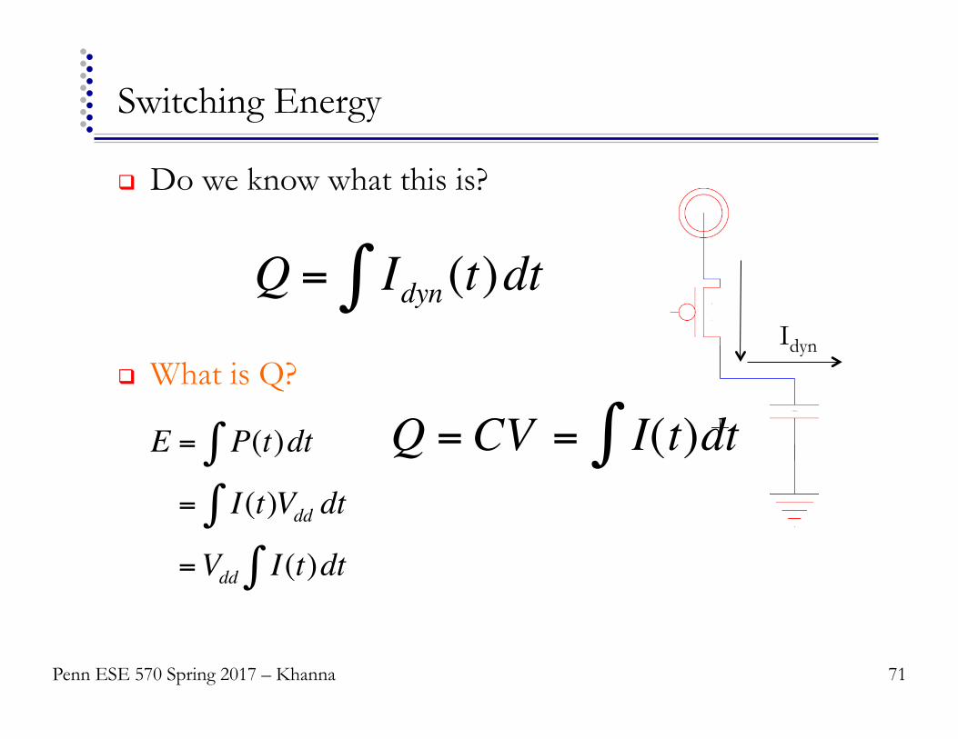
Switching Energy
71
! Do we know what this is?
! What is Q? Idyn
Q = Idyn (t)dt∫
E = P(t)dt∫= I(t)Vdd dt∫=Vdd I(t)dt∫
€
Q = CV = I(t)dt∫
Penn ESE 570 Spring 2017 – Khanna

Switching Energy
72
! Do we know what this is?
! What is Q? Idyn
Q = Idyn (t)dt∫
E = P(t)dt∫= I(t)Vdd dt∫=Vdd I(t)dt∫
€
Q = CV = I(t)dt∫
€
E = CVdd2
Capacitor charging energy
Penn ESE 570 Spring 2017 – Khanna

Switching Power
! Every time output switches 0#1 pay: " E = CV2
! Pdyn = (# 0#1 trans) × CV2 / time
! # 0#1 trans = ½ # of transitions
! Pdyn = (# trans) × ½CV2 / time
73 Penn ESE 570 Spring 2017 – Khanna

Switching
74
Short Circuit Power
Penn ESE 570 Spring 2017 – Khanna

Short Circuit Power
! Between VTN and Vdd - VTP
" Both N and P devices conducting
75 Penn ESE 570 Spring 2017 - Khanna

Short Circuit Power
! Between VTN and Vdd - VTP
" Both N and P devices conducting
! Roughly:
76
Isc
Vin
time
Vout
Isdp
time
time
time
Vthn
Vdd
Vdd
Vdd-Vthp
Isc
tsc tsc Penn ESE 570 Spring 2017 – Khanna

Peak Current
! Ipeak around Vdd/2 " If |VTN|=|VTP| and sized equal rise/fall
77
€
IDS ≈νsatCOXW VGS −VT −VDSAT
2%
& '
(
) *
Vin
time
Vout
Isdp
time
time
time
Vthn
Vdd
Vdd
Vdd-Vthp
Isc
tsc tsc Penn ESE 570 Spring 2017 – Khanna

Peak Current
! Ipeak around Vdd/2 " If |VTN|=|VTP| and sized equal rise/fall
78
€
IDS ≈νsatCOXW VGS −VT −VDSAT
2%
& '
(
) *
€
I(t)dt∫ ≈ Ipeak × tsc ×12%
& ' (
) *
Vin
time
Vout
Isdp
time
time
time
Vthn
Vdd
Vdd
Vdd-Vthp
Isc
tsc tsc Penn ESE 570 Spring 2017 – Khanna

Vin
time
Vout
Isdp
time
time
time
Vthn
Vdd
Vdd
Vdd-Vthp
Isc
tsc tsc
Peak Current
! Ipeak around Vdd/2 " If |VTN|=|VTP| and sized equal rise/fall
79
€
IDS ≈νsatCOXW VGS −VT −VDSAT
2%
& '
(
) *
€
I(t)dt∫ ≈ Ipeak × tsc ×12%
& ' (
) *
€
E =Vdd × Ipeak × tsc ×12#
$ % &
' (
Penn ESE 570 Spring 2017 – Khanna

Short Circuit Energy
! Make it look like a capacitance, CSC
" Q=I×t " Q=CV
80
E =Vdd × I peak × tsc ×12"
#$%
&'
"
#$
%
&'
E =Vdd ×QSC
E =Vdd × (CSCVdd ) =CSCV2dd
Penn ESE 570 Spring 2015 - Khanna

Short Circuit Energy
! Every time switch " Also dissipate short-circuit energy: E = CV2
" Different C = Csc
" Ccs “fake” capacitance (for accounting)
81 Penn ESE 570 Spring 2017 - Khanna

Switching Power
! Every time output switches 0#1 pay: " E = CV2
! Pdyn = (# 0#1 trans) × CV2 / time
! # 0#1 trans = ½ # of transitions
! Pdyn = (# trans) × ½CV2 / time
82 Penn ESE 570 Spring 2017 – Khanna

Charging Power
! Pdyn = (# trans) × ½CV2 / time ! Often like to think about switching frequency ! Useful to consider per clock cycle
" Frequency f = 1/clock-period
! Pdyn = (#trans/clock) ½CV2 f
83 Penn ESE 570 Spring 2017 – Khanna

Switching Power
! Pdyn = (#trans/clock) ½CV2 f ! Let a = activity factor
a = average #tran/clock
! Pdyn = a½CV2 f ! Psc = aCscV2 f
84 Penn ESE 570 Spring 2017 – Khanna

Switching Power
! Pdyn = (#0#1 trans/clock) CV2 f ! Let a = activity factor
a = average #tran0#1/clock
! Pdyn = aCV2 f ! Psc = aCscV2 f
85 Penn ESE 570 Spring 2017 - Khanna

Activity Factor
! Let a = activity factor " a = average #tran0#1/clock
Penn ESE 570 Spring 2017 - Khanna 86
a = p(outi = 0)p(outi+1 =1)
a = N0
2NN12N
=N0 (2
N − N0 )22N

Reduce Dynamic Power?
! Pdyn = aCV2 f
! How do we reduce dynamic power?
87 Penn ESE 570 Spring 2017 - Khanna

Reduce Activity Factor
Penn ESE 570 Spring 2017 - Khanna 88
A B
C D
O1
O2
F
A B
C
D
O1
O2
F
Tree Chain
a = p(outi = 0)p(outi+1 =1)
a = N0
2NN12N
=N0 (2
N − N0 )22N

Reduce Activity Factor
Penn ESE 570 Spring 2017 - Khanna 89
A B
C D
O1
O2
F
A B
C
D
O1
O2
F
Tree Chain
3/16
7/64
15/256
a = p(outi = 0)p(outi+1 =1)
a = N0
2NN12N
=N0 (2
N − N0 )22N

Reduce Activity Factor
Penn ESE 570 Spring 2017 - Khanna 90
A B
C D
O1
O2
F
A B
C
D
O1
O2
F
Tree Chain
3/16
7/64
15/256
a = p(outi = 0)p(outi+1 =1)
a = N0
2NN12N
=N0 (2
N − N0 )22N
3/16
3/16
15/256

Total Power
! Ptot = Pstatic + Psc + Pdyn
! Psw = Pdyn + Psc = a(CloadV2f) + CscV2f
! Ptot ≈ a(CloadV2f) + CscV2f + VI’s(W/L)e-Vt/(nkT/q)
! Let a = activity factor a = average #tran0#1/clock
91 Penn ESE 570 Spring 2017 – Khanna

Energy and Power Optimization
Penn ESE 570 Spring 2017 – Khanna

Power Sources
Review: Ptot = Pstatic + Pdyn + Psc
Penn ESE 570 Spring 2017 – Khanna

Worksheet Problem 1
Vin Istatic Idynamic Isc
0V
140mV
400mV
500mV
600mV
860mV
1V
94 Penn ESE 570 Spring 2017 – Khanna

Worksheet Problem 1
Vin Istatic Idynamic Isc
0V 180pA 126uA
140mV 6nA 100uA
400mV 36uA 18uA
500mV 36uA
600mV 36uA 18uA
860mV 6nA 100uA
1V 180pA 126uA
95 Penn ESE 570 Spring 2017 – Khanna

Idea
! CMOS " Design for worst case input switching case and delay
! There are other logic disciplines " Ratioed logic " Can use pass transistors for logic
" Transmission gates " Will see in use in dynamic logic
! Gate layout optimization " Euler Paths
! Power Basics Review
96 Penn ESE 570 Spring 2017 – Khanna

Admin
! HW 6 " Out now " Due Tuesday 3/28
97 Penn ESE 570 Spring 2017 - Khanna
Recommended