PREFERENTIAL NUCLEATION OF COBALT NANOCLUSTERS ON THE
FACETED RHENIUM (1231) SURFACE
By
MERAL REYHAN
A thesis submitted to the
Graduate School-New Brunswick
Rutgers, The State University of New Jersey
in partial fulfillment of the requirements
for the degree of
Master of Science
Graduate Program in Physics
written under the direction of
Professor Ted Madey
and approved by
________________________
________________________
________________________
New Brunswick, New Jersey
October, 2007
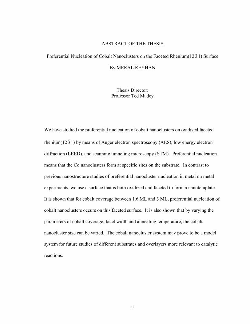
ABSTRACT OF THE THESIS
Preferential Nucleation of Cobalt Nanoclusters on the Faceted Rhenium(1231) Surface
By MERAL REYHAN
Thesis Director: Professor Ted Madey
We have studied the preferential nucleation of cobalt nanoclusters on oxidized faceted
rhenium(1231) by means of Auger electron spectroscopy (AES), low energy electron
diffraction (LEED), and scanning tunneling microscopy (STM). Preferential nucleation
means that the Co nanoclusters form at specific sites on the substrate. In contrast to
previous nanostructure studies of preferential nanocluster nucleation in metal on metal
experiments, we use a surface that is both oxidized and faceted to form a nanotemplate.
It is shown that for cobalt coverage between 1.6 ML and 3 ML, preferential nucleation of
cobalt nanoclusters occurs on this faceted surface. It is also shown that by varying the
parameters of cobalt coverage, facet width and annealing temperature, the cobalt
nanocluster size can be varied. The cobalt nanocluster system may prove to be a model
system for future studies of different substrates and overlayers more relevant to catalytic
reactions.
ii

Acknowledgement
This work would have been impossible without the support and guidance of
Professor Theodore Madey during my studies at Rutgers University. I would like to
thank Dr. Madey for giving me the opportunity to work in his group, which was a great
experience for me. I would also like to thank Mr. Hao Wang for introducing me to the
experimental setup and all its secrets, for his patience and advice. I would like to thank
my family for all of their support during my academic career. I would especially like to
thank Cassie for letting me accompany her on long walks around the neighborhood.
iii
Table of Contents
Abstract ii
Acknowledgements iii
List of Tables vi
List of Illustrations vii
1. Introduction 1
2. Growth and Nucleation 7
3. Materials 13
4. Instrumentation, Cleaning process, and Characterization Techniques 16
4.1 Introduction 16
4.2 Cleaning Process 18
4.3.1 Low Energy Electron Diffraction 19
4.3.2 Auger Electron Spectroscopy 22
4.3.3 Scanning Tunneling Microscopy 26
5. Oxygen Induced Faceting of Re(1231) 31
6. Preferential Nucleation of Co Nanoclusters on Re(1231) 38
6.1 Introduction 38
6.2 Cleaning Process 38
6.3 Experimental Procedure 38
6.3.1 Controlling Cluster Size 43
6.4 Discussion of Cluster Statistics 46
7. Conclusion 55
References 56
iv

Appendix 58
v
Lists of Tables
Table 1 Experimental Parameters for Faceted Rhenium 34
Table 2 Experimental Parameters for Cobalt Nanocluster Nucleation 39
Table 3 Cobalt Nanocluster Parameters 46
Table 4 Histograms of Nanocluster Length 48
Table 5 Histograms of Nanocluster Width 49
Table 6 Histograms of Nanocluster Height 50
Table 7 Estimate of total Co within the nanoclusters 53
vi
List of Illustrations
Figure 1. Copper nanochains were aggregated on the Pd 2 Figure 2. Co chains form at the step edges of the Pt surface 4 Figure 3. Co monatomic chains 5 Figure 4. Rhenium Facets 6 Figure 5. Different growth modes 8 Figure 6. Homogeneous nucleation 9 Figure 7. Critical nucleus size graph 10 Figure 8. Ehrlich-Schwoebel barrier at the descending step edges 11 Figure 9. Preferential nucleation of Co 12 Figure 10. The reforming catalytic process 14 Figure 11. The experimental chamber 17 Figure 12. Front view port chamber view 17 Figure. 13. Schematic of diffraction 20 Figure. 14. The LEED optics 22 Figure 15. Schematic of the Auger process 23 Figure 16. This is an Auger spectrum for clean Rhenium 25 Figure 17. Cobalt coverage versus time graph 26 Figure 18. STM tip probing a surface 27 Figure 19. Clustering on the rhenium surface 30 Figure 20. Atomic organization of Re(1231) and stereographic projection 32 Figure 21. LEED pattern of rhenium (1231) 34 Figure 22. STM images of faceted Rhenium surface 35
vii
Figure 23. Cobalt on faceted O/Re 40 Figure 24. STM image of Experiment 1 41 Figure 25. A 3-D rendering of Experiment 1 42 Figure 26. STM image of Experiment 2 43 Figure 27. STM image of Experiment 3 45 Figure 28. STM image of Experiment 4 46 Figure 29. Cluster Length and Width 47 Figure 30. Scan Line Analysis Technique 47
viii
1
Chapter 1
Introduction
Applications for nanowires are limited only by the imagination. Nanowires are
currently being used in electronics, optics, mechanics, catalysis, and sensing technology.
These wires are capable of connecting with different kinds of molecules that compose the
human body having applications as biological sensors for measuring anything from
certain hormone levels in pregnant women to glucose levels in diabetics [6]. Nanowires
composed of different materials have different properties, further augmenting their
applications. These wires are the building blocks for future nanoscale devices. Due to
the rapidly growing interest, new techniques for nanowire creation are necessary.
Currently nanowires are created in a myriad of ways; amongst the most common
ways are suspension and synthesis. A suspended nanowire is often produced by
chemical etching of a larger wire or showering energetic particles on a larger wire under
vacuum conditions. Another popular technique for the creation of suspended nanowires
is using a Scanning Tunneling Microscope (STM) on the surface of a metal heated near
its melting point. By contacting the tip of the STM on the surface of this metal and then
retracting the tip, a nanowire can be drawn from the metal’s surface [26].
Another common method for creating nanowires is synthesis. A popular
synthesis technique is called the Vapor-Liquid-Solid (VLS) synthesis method. This
method uses a source material such as a feed gas or laser ablated (dissipated by melting)
particles. The source is exposed to a catalyst, such as liquid metal nanoclusters, which
enters the nanocluster and begins to saturate it. Once the nanocluster is supersaturated,
2
the source solidifies and grows outward. By controlling the amount of the source that is
used, the shape and height of the nanowire can be regulated [9].
Vapor deposition is a technique that is frequently used to create nanowires.
Evaporative deposition is a process in which a thin film of metal is deposited onto a
substrate by being converted into a vapor, then being transported through a region of low
pressure to the substrate’s surface, and finally condensing on the substrate forming a film
[29]. In the present experiment, this is the primary technique used for delivering atoms
to the substrate. Another deposition technique, known as electrochemical deposition is
frequently used in the creation of nanowires. A metal surface for deposition is connected
to the negative terminal of a voltage source and the metal to be deposited is connected to
the positive terminal. The two objects are placed in an electrolyte and when the battery is
turned on, a current passes through the electrolyte, which reduces the metal ions to be
deposited forming a solid metal on the desired surface [20].
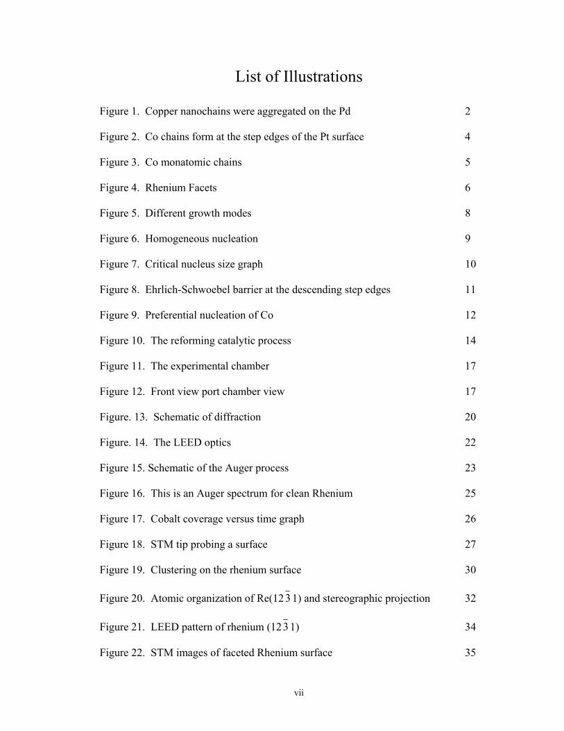
One of the first scientists to grow nanowires was Dr. H. Roeder. In his paper
published in 1993, “Building One- and Two-Dimensional Nanostructures by Diffusion-
Controlled Aggregation at Surfaces”, he was able to aggregate Cu in the (110) channels
of a Pd(110) substrate. From Roeder’s paper, many other scientists were inspired to
further the study of nanostructures. The following picture is from Roeder’s paper
illustrating the Cu chains on Pd(110) [23].
Figure 1. The copper nanochains [24] were aggregated on the Pd(110)substrate by controlled
3
While it looks like only certain channels have Cu chains within them, this is not
true. Since the image is displayed on such a limited scale, it is difficult to see that all the
channels have Cu chains in them [23].
The mechanism for the growth of the chains is thought to be caused by the
collision of two diffusing Cu atoms, which form a relatively immobile nucleus. Once the
Cu nucleus is trapped in a channel, more diffusing Cu atoms congregate around this
single nucleus. This in turn leads to Cu atom chains of variable lengths. By varying the
deposition temperature, they were able to change the average lengths of the Cu chains.
For temperatures of 300 K, the average Cu chains are hundreds of Angstroms (Å) long.
For temperatures less than 300 K, a Cu chain’s average length decreased to tens of atoms
in length. For temperatures greater than 300 K, islands of Cu formed. The primary
measuring technique used in this paper was scanning tunneling microscopy [23].
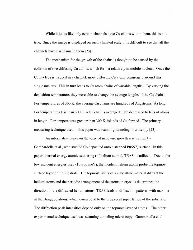
An informative paper on the topic of nanowire growth was written by
Gambardella et al., who studied Co deposited onto a stepped Pt(997) surface. In this
paper, thermal energy atomic scattering (of helium atoms), TEAS, is utilized. Due to the
low incident energies used (10-300 meV), the incident helium atoms probe the topmost
surface layer of the substrate. The topmost layers of a crystalline material diffract the
helium atoms and the periodic arrangement of the atoms in crystals determines the
direction of the diffracted helium atoms. TEAS leads to diffraction patterns with maxima
at the Bragg positions, which correspond to the reciprocal super lattice of the substrate.
The diffraction peak intensities depend only on the topmost layer of atoms. The other
experimental technique used was scanning tunneling microscopy. Gambardella et al.
4
were able to show periodic arrays formed between temperatures of 250 to 300 K. The
cobalt formed nanowires along the step-edges. The following picture is an atomically
resolved STM image of Co wires on Pt(997) [7].
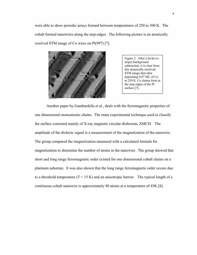
Another paper by Gambardella et al., deals with t
one dimensional monoatomic chains. The main experim
the surface consisted mainly of X-ray magnetic circular d
amplitude of the dichroic signal is a measurement of the
The group compared the magnetization measured with a
magnetization to determine the number of atoms in the n
short and long range ferromagnetic order existed for one
platinum substrate. It was also shown that the long range
to a threshold temperature (T < 15 K) and an anisotropic
continuous cobalt nanowire is approximately 80 atoms at
Figure 2. After a dz/dx (x-slope) background subtraction, it is clear from this atomically resolved STM image that after depositing 0.07 ML of Co at 250 K, Co chains form atthe step edges of the Pt surface [7].
he ferromagnetic properties of
ental technique used to classify
ichroism, XMCD. The
magnetization of the nanowire.
calculated formula for
anowire. The group showed that
dimensional cobalt chains on a
ferromagnetic order occurs due
barrier. The typical length of a
a temperature of 45K [8].
5
Figure 3a. The original stepped surface before Co deposition. Figure 3b. Co monatomic chains decorate the step edges of the Pt surface after 0.13 ML of Co is evaporated onto the substrate held at 260K [8].
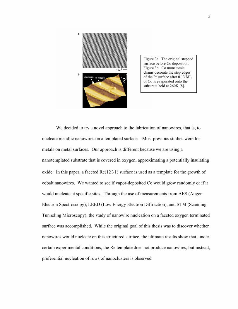
We decided to try a novel approach to the fabrication of nanowires, that is, to
nucleate metallic nanowires on a templated surface. Most previous studies were for
metals on metal surfaces. Our approach is different because we are using a
nanotemplated substrate that is covered in oxygen, approximating a potentially insulating
oxide. In this paper, a faceted Re(123 1) surface is used as a template for the growth of
cobalt nanowires. We wanted to see if vapor-deposited Co would grow randomly or if it
would nucleate at specific sites. Through the use of measurements from AES (Auger
Electron Spectroscopy), LEED (Low Energy Electron Diffraction), and STM (Scanning
Tunneling Microscopy), the study of nanowire nucleation on a faceted oxygen terminated
surface was accomplished. While the original goal of this thesis was to discover whether
nanowires would nucleate on this structured surface, the ultimate results show that, under
certain experimental conditions, the Re template does not produce nanowires, but instead,
preferential nucleation of rows of nanoclusters is observed.
6
Figure 4 shows a schematic diagram of the facets which form on Re(123 1), after
the deposition of oxygen and heating in vacuum. As will be discussed in more detail
below, long ridges containing (011 0) and (11 2 1) oriented facets cover the surface.
When Co is deposited and the surface is annealed, we do not see nanowires of Co that
nucleate at sites in the bottoms of the troughs (Figure 4 b). However, we do see
nanoclusters of Co which preferentially nucleate in the troughs of the facets (Figure 4 c).
Atomic Structure of (11-21)
Atomic Structure of (01-10)
)0101(
)1211(
a)
c) b)
Figure 4. Illustration a) shows the faceted Re(12-31) surface and the atomic structure of the two facets. Illustration b) depicts possible nucleation sites for the Co nanowires with black and gray ‘wires’. Illustration c) shows the preferential nucleation site of the Co nanoclusters.
7
Chapter 2
Growth and Preferential Nucleation
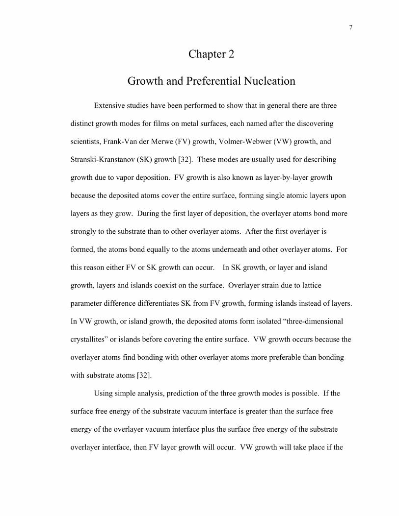
Extensive studies have been performed to show that in general there are three
distinct growth modes for films on metal surfaces, each named after the discovering
scientists, Frank-Van der Merwe (FV) growth, Volmer-Webwer (VW) growth, and
Stranski-Kranstanov (SK) growth [32]. These modes are usually used for describing
growth due to vapor deposition. FV growth is also known as layer-by-layer growth
because the deposited atoms cover the entire surface, forming single atomic layers upon
layers as they grow. During the first layer of deposition, the overlayer atoms bond more
strongly to the substrate than to other overlayer atoms. After the first overlayer is
formed, the atoms bond equally to the atoms underneath and other overlayer atoms. For
this reason either FV or SK growth can occur. In SK growth, or layer and island
growth, layers and islands coexist on the surface. Overlayer strain due to lattice
parameter difference differentiates SK from FV growth, forming islands instead of layers.
In VW growth, or island growth, the deposited atoms form isolated “three-dimensional
crystallites” or islands before covering the entire surface. VW growth occurs because the
overlayer atoms find bonding with other overlayer atoms more preferable than bonding
with substrate atoms [32].
Using simple analysis, prediction of the three growth modes is possible. If the
surface free energy of the substrate vacuum interface is greater than the surface free
energy of the overlayer vacuum interface plus the surface free energy of the substrate
overlayer interface, then FV layer growth will occur. VW growth will take place if the
8
surface free energy of the substrate vacuum interface is less than the surface free energy
of the overlayer vacuum interface plus the surface free energy of the substrate overlayer.
If the surface free energy of the substrate vacuum interface is approximately equal to the
surface free energy of the overlayer vacuum interface plus the surface free energy of the
substrate overlayer, then SK growth will occur [32]. Although, these three modes are
thermodynamic equilibrium modes, even away from equilibrium this is a useful
classification.
Th
small stab
surface. A
nuclei, ul
divided in
Homogen
defect fre
random s
irregulari
and terrac
Figure 5. The three different growth modes are illustrated by block models.
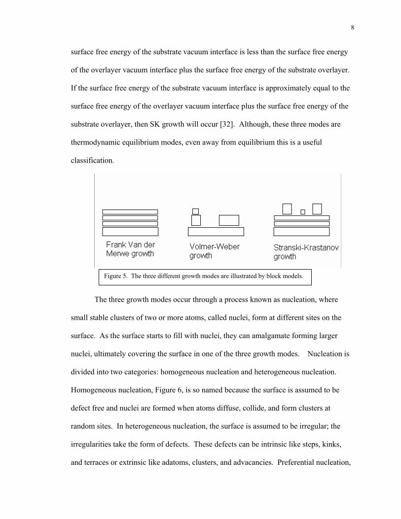
e three growth modes occur through a process known as nucleation, where
le clusters of two or more atoms, called nuclei, form at different sites on the
s the surface starts to fill with nuclei, they can amalgamate forming larger
timately covering the surface in one of the three growth modes. Nucleation is
to two categories: homogeneous nucleation and heterogeneous nucleation.
eous nucleation, Figure 6, is so named because the surface is assumed to be
e and nuclei are formed when atoms diffuse, collide, and form clusters at
ites. In heterogeneous nucleation, the surface is assumed to be irregular; the
ties take the form of defects. These defects can be intrinsic like steps, kinks,
es or extrinsic like adatoms, clusters, and advacancies. Preferential nucleation,
9
a form of heterogeneous nucleation, implies that there are particular sites on the
substrate’s surface at which nucleation occurs the most frequently [19].
Figure 6. Atoms are deposited and then diffuse on a defect free surface, illustrating homogeneous nucleation [19].
Homogeneous nucleation occurs when atoms diffuse on a surface to form nuclei.
The nuclei are formed after deposited atoms collide and remain stuck together. After
several collisions, the atoms begin to form a cluster. The radius of the cluster is governed
by energetics, which determines when a stable nucleus size is reached. This minimum
radius size, known as the critical cluster size, can be determined by the following formula
for total free energy:
Volume Free Energy Surface free Energy
.
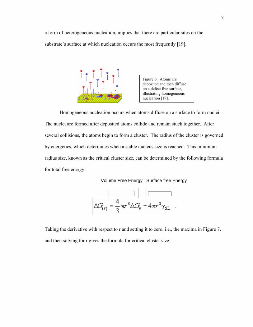
Taking the derivative with respect to r and setting it to zero, i.e., the maxima in Figure 7,
and then solving for r gives the formula for critical cluster size:
.
10
Figure 7. Critical nucleus size can be determined from this energy versus radius graph.
If the cluster radius, r, is greater than the critical cluster size, r*, then the nucleus is stable
and if it is less than the critical cluster size, r*, the nucleus is unstable. The critical
cluster size is a key factor in homogeneous nucleation [19]. For many systems, the
critical cluster size is one or two atoms.
Adopting a model where homogeneous nucleation occurs in the first layer and
adatoms desorb slowly, the saturation density (nuclei/unit area), N, of nuclei can be
calculated. The saturation density is then reached when the diffusing atoms find an
existing nucleus before finding another diffusing atom with which forming a new nucleus
is possible. The formula used to calculate N is:
N~(F/D)(x)exp{Ei/((i+2)*kT)},
where F is the vapor deposition flux (atoms/area/second), D is the diffusion coefficient, i
is the number of atoms in the critical nucleus, Ei is the critical nucleus binding energy,
and exponent x=i/(i+2). From this formula, it is clear that the saturation density increases
with vapor flux and binding energy and decreases with increasing diffusion coefficient
and temperature.
The Ehrlich-Schwoebel barrier controls heterogeneous nucleation. Once atoms
are deposited on the heterogeneous substrate surface, they begin to diffuse. In the case of
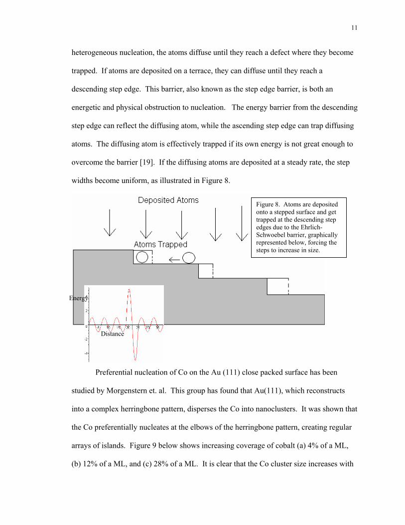
11
heterogeneous nucleation, the atoms diffuse until they reach a defect where they become
trapped. If atoms are deposited on a terrace, they can diffuse until they reach a
descending step edge. This barrier, also known as the step edge barrier, is both an
energetic and physical obstruction to nucleation. The energy barrier from the descending
step edge can reflect the diffusing atom, while the ascending step edge can trap diffusing
atoms. The diffusing atom is effectively trapped if its own energy is not great enough to
overcome the barrier [19]. If the diffusing atoms are deposited at a steady rate, the step
widths become uniform, as illustrated in Figure 8.
Figure 8. Atoms are deposited onto a stepped surface and get trapped at the descending step edges due to the Ehrlich-Schwoebel barrier, graphically represented below, forcing the steps to increase in size.
Energy
P
studied
into a co
the Co p
arrays o
(b) 12%
Distance
referential nucleation of Co on the Au (111) close packed surface has been
by Morgenstern et. al. This group has found that Au(111), which reconstructs
mplex herringbone pattern, disperses the Co into nanoclusters. It was shown that
referentially nucleates at the elbows of the herringbone pattern, creating regular
f islands. Figure 9 below shows increasing coverage of cobalt (a) 4% of a ML,
of a ML, and (c) 28% of a ML. It is clear that the Co cluster size increases with
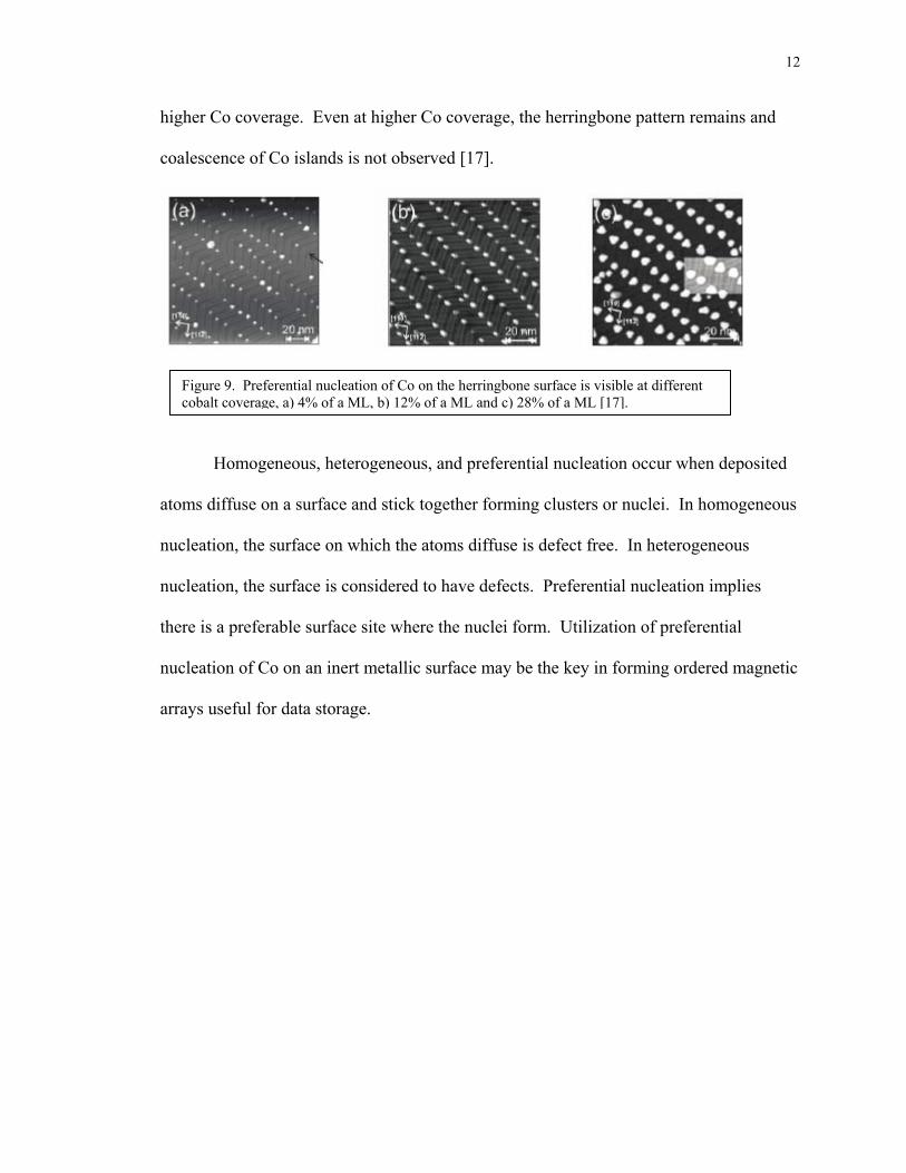
12
higher Co coverage. Even at higher Co coverage, the herringbone pattern remains and
coalescence of Co islands is not observed [17].
Figure 9. Preferential nucleation of Co on the herringbone surface is visible at different cobalt coverage, a) 4% of a ML, b) 12% of a ML and c) 28% of a ML [17].
Homogeneous, heterogeneous, and preferential nucleation occur when deposited
atoms diffuse on a surface and stick together forming clusters or nuclei. In homogeneous
nucleation, the surface on which the atoms diffuse is defect free. In heterogeneous
nucleation, the surface is considered to have defects. Preferential nucleation implies
there is a preferable surface site where the nuclei form. Utilization of preferential
nucleation of Co on an inert metallic surface may be the key in forming ordered magnetic
arrays useful for data storage.
13
Chapter 3
Materials
Rhenium is an important element with applications from catalysis to super
conductivity. Rhenium, element 75, is a dense, hexagonal close packed transition metal.
It is the substrate material used throughout this experiment. The surface orientation of
this substrate is the (123 1). Rhenium was the last naturally occurring element to be
discovered. At approximately one part per billion, rhenium is widely spread throughout
the Earth’s crust. Typically, a platinum-rhenium catalyst is used to make lead-free high-
octane gasoline in a reforming process [22]. Catalysis refers to the acceleration of a
chemical reaction by means of a substance that is not consumed by the overall reaction.
In the case of heterogeneous catalysis, the catalyst provides the surface on which
the reactants are temporarily absorbed. (By adding nanostructures, this surface is
changed.) The bonds in the reactants weaken enough for new bonds to be created. The
bonds between the reactants and the catalyst are weaker than the bonds between the
reactants, so the reactant product is released. Depending on the form of adsorption,
Langmuir-Hinshelwood or Eley-Rideal mechanisms occur. In the Langmuir-
Hinshelwood mechanism both molecules adsorb and react on the surface, while in the
Eley-Rideal mechanism only one molecule adsorbs and reaction occurs when a gaseous
molecule collides with it.
The reforming catalytic process takes straight chain hydrocarbons in the C6 to C8
range from the gasoline or naphtha fractions and rearranges them into compounds
containing benzene rings. Hydrogen is produced as a by-product of the reactions.
14
R
tungsten a
is often u
only by p
the larges
tungsten-
Th
10 mm in
aligned w
Pr
and annea
surface is
formation
C
element 2
This mea
remain m
physical o
the Pauli
Figure 10. The reforming catalytic process transforms hydrocarbons into benzene rings and hydrogen.
henium has the third highest melting-point of all elements, bested only by
nd carbon. The melting point of rhenium is 3459 K. For this reason, rhenium
sed in jet engine parts. Rhenium is also one of the densest elements, exceeded
latinum, iridium, and osmium. Its density is 21.02 g cm-3. Rhenium also has
t number of oxidation states of any known element. Rhenium-molybdenum and
rhenium alloys are superconducting [22].
e rhenium crystal used in this study has a purity of 99.99%. It is approximately
diameter. The thickness of the crystal is approximately 1.5 mm. The crystal is
ithin 0.5 degrees of the (123 1) orientation.
evious experiments performed by Hao Wang have shown that after oxidation
ling, facets will form on the rhenium substrate. The faceted oxidized rhenium
the proposed template for cobalt nanostructure growth. More detail on facet
will be discussed in chapter 5.
obalt is the element used for formation of nanoclusters on faceted Re. Cobalt,
7, has a hexagonal close packed structure [2]. It is a ferromagnetic element.
ns that an external magnetic field can magnetize cobalt and the cobalt will
agnetized for a period of time after it is removed from the magnetic field. The
rigin of this magnetization is from quantum mechanics, in particular, spin and
Exclusion Principle [12].
15
Cobalt’s ferromagnetic properties make it an interesting element to study. In
addition, cobalt nanostructures are of particular interest for high-density magnetic data
storage [17]. A future experiment studying the ferromagnetic properties of cobalt
nanostructures on a templated surface could be performed to aid in the understanding of
how nanostructures affect the catalytic process.
Cobalt also has interesting catalytic properties. It is a major component of CoMo
catalysts used for hydrodesulfurization. This catalytic process is used to remove sulfur
from natural gas and from refined petroleum products like gasoline, kerosene, and diesel
fuel. By removing the sulfur from the petroleum feed stocks, sulfur dioxide emissions
from cars, trains, planes, etc. can be reduced [2]. In general, nanoarchitecture has been
shown to enhance the selectivity, ability to produce one specific molecule out of a
number of thermodynamically feasible products, of catalytic processes [25].
The goal of the present experiment is not to make catalysts or magnetic devices.
Rather, it is to see how formulation of an oxygen-covered nanotemplate (faceted Re)
affects the nucleation and growth of a sample vapor-deposited metal (Co). If we find
evidence of preferential nucleation, it will have implications for other more useful
metal/substrate combinations.
16
Chapter 4
Instrumentation, Cleaning Process, and Characterization of Techniques
The techniques of Low Energy Electron Diffraction (LEED), Auger Electron
Spectroscopy (AES), and Scanning Tunneling Microscopy (STM), which were used to
acquire data for the majority of this thesis, are described in the following sections. These
procedures are highly surface sensitive and frequently used to study surfaces and surface
processes.
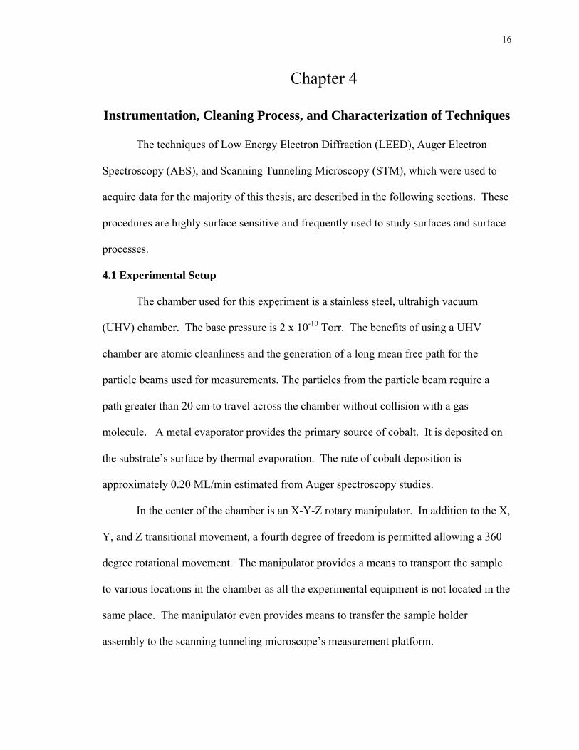
4.1 Experimental Setup
The chamber used for this experiment is a stainless steel, ultrahigh vacuum
(UHV) chamber. The base pressure is 2 x 10⁻¹⁰ Torr. The benefits of using a UHV
chamber are atomic cleanliness and the generation of a long mean free path for the
particle beams used for measurements. The particles from the particle beam require a
path greater than 20 cm to travel across the chamber without collision with a gas
molecule. A metal evaporator provides the primary source of cobalt. It is deposited on
the substrate’s surface by thermal evaporation. The rate of cobalt deposition is
approximately 0.20 ML/min estimated from Auger spectroscopy studies.
In the center of the chamber is an X-Y-Z rotary manipulator. In addition to the X,
Y, and Z transitional movement, a fourth degree of freedom is permitted allowing a 360
degree rotational movement. The manipulator provides a means to transport the sample
to various locations in the chamber as all the experimental equipment is not located in the
same place. The manipulator even provides means to transfer the sample holder
assembly to the scanning tunneling microscope’s measurement platform.
17
To measure the pressure in the chamber, an uncalibrated Bayard-Alpert ionization
gauge is used. A filament for electron bombardment heating of the Re sample is biased
to a high voltage (-1.5 kV) and is located behind the substrate surface. Another filament
is located in the chamber and is typically used for cleaning purposes.
Sampleand Ho
Ionization Vacuum Gauge
Rear View Low Energy Electron Diffraction (LEED) Optics
Scanning tunneling Microscope (STM)
Sample Holder “Parking Lot” Electron B
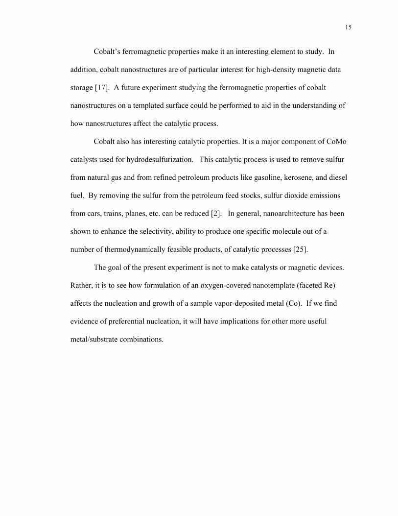
Figure 11. This is the chamber that was used to conduct the experiments for this thesis.
Manipulator lder
Cobalt Evaporator
Auger Electron Spectroscopy (AES) Assembly
ombardment Heating Filament
Figure 12. Looking through the front view port, the inside of the chamber and all of the equipment used for this thesis is visible.
18
4.2 Sample Cleaning
Cleanliness is highly important when studying the physical and electronic
properties of a surface. The presence of impurities affects the physical properties of the
surface studied. After heating a crystal to high temperatures, bulk impurities will often
find their way to the surface [30]. Sulfur, nitrogen, oxygen, and carbon are the
particular impurities found on the Re crystal used in this study. The sulfur and nitrogen
contaminants are the results of previous experiments performed in the UHV chamber
used for this study.
The oxygen contamination is not a particular problem, as the surface requires
oxygen to induce faceting. The carbon impurities, however, inhibit the faceting process
and must be reduced as much as possible. To remove the carbon surface contaminants,
flash heating in oxygen is required. The carbon reacts with the oxygen to desorb as CO.
The remaining oxygen on the surface is not a problem due to the reasons described
above.
To clean a sample, an electron beam is used to heat the sample to temperatures
greater than 2200K. In order to complete this process, a filament is positioned in front of
the sample and a current is applied to the filament in order to remove contaminants from
the surface. This heating procedure is continued until the Auger spectrum shows low
levels of contamination. If the residual contaminant species, mainly carbon, are smaller
than a few percent of a monolayer of atoms, the experiment is continued. The cleanliness
of the surface is double checked with LEED patterns. The typical conditions used for e-
beam cleaning are provided in chapter 6, section 2.
19
4.3.1 Low Energy Electron Diffraction
The highly surface sensitive method known as low energy electron diffraction
(LEED) is used to investigate the periodic arrays on the surface of a crystal. Making use
of the de Broglie relation, this method uses electrons to hit the crystal’s surface with a
wavelength approximately 0.64 to 3.9 Angstroms and electron energies from 20 eV to
800 eV. This size wavelength is a good match for interatomic spacing on surfaces. The
mechanism behind this technique is as follows: low energy electrons bombard the crystal
surface resulting in both elastic and inelastic scattering. Since the mean free path of the
inelastic scattering is on the order of 5 to 10 Angstroms, the elastically backscattered
electrons dominate the system and are diffracted onto a fluorescent screen. The
backscattered electrons reveal the surface lattice structure in reciprocal space on the
screen. The relationship between the unit cell in real space and reciprocal space is
logical: the distance, d, between atoms in a unit cell in real space transforms to the
reciprocal of that distance (1/d) in reciprocal space. Using conservation of energy and
momentum, one can determine the surface structure of a crystal [29].
The wavelength of the electron is defined by the de Broglie relation:
λ=h/p,
where h is Planck’s constant, and p is momentum. From the definition of momentum a
relationship between electron energy and wavelength can be derived,
p=mv=(2 meEK)1/2 , λ=h/(2 meEK)1/2
where me is the mass of an electron, v is velocity, and EK is the kinetic energy of the
electron. If the incident electron approach the surface from the normal direction and
20
scatter from the surface with angle θ from the surface normal, the path length difference
can be defined as
d= a sin θ,
where a is the distance between atoms in a one-dimensional periodic array at the surface.
When the path length difference is an integer multiple of the electron wavelength,
constructive interference occurs. This is known as the Bragg condition, given by the
following formula:
a sin θ=n λ,
where n is an integer [29].
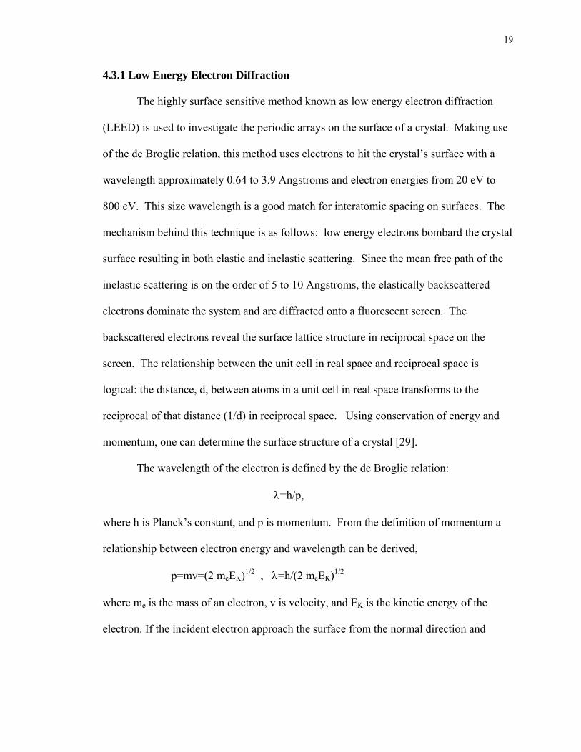
Using the derivation above, the diffraction pattern for a 2-D array can be
obtained. The figure below, Figure 13, illustrates a surface unit cell contained by vectors
a1 and a2. The electron wave is depicted by the incoming vector K and the outgoing
vector K ′ .
Figure 13. a) Schematic of diffraction from a 1-D array of atoms b) A surface unit cell of a rectangular array of atoms, with lattice vectors a1 and a2
21
The equation derived previously, using Bragg’s condition can now be extended
for interference in 2 dimensions as follows:
ai sin θ=n λ ,
(ai sin θ)(2π/ λ)=2π n,
θλπθ sin )2( asin a a i ii =′=
′• KK
where i = 1 or 2, n is an integer, and vectors ia and K ′ are defined by Figure 13. The
equation above is satisfied by the condition:
)(2 21 gmgnKKK + = )−′( =′∆ |||| π
where n and m are integers that fulfill Bragg’s condition and (1/ai )=gi is the reciprocal
unit cell vector.
In principle, one can make careful current and voltage measurements of the LEED
beams and fit the data using multiple scattering theory to obtain the surface structure. In
the present case, LEED is used to identify the symmetry of the surface unit cell to
determine surface cleanliness and to tell whether or not facets have formed.
By varying the energy range of the electron gun, facets can be observed. To
perform this procedure, pictures of LEED patterns are taken at different electron energy
values. As the electron energy is increased, the constructive diffraction pattern spots
move toward specular poles. On the faceted Re(123 1) surface, two specular poles are
observed and are associated with the (011 0) and (11 2 1) facets. These same two poles
are observed after oxygen is dosed on a faceted Re(123 1) surface [29]. Princeton
22
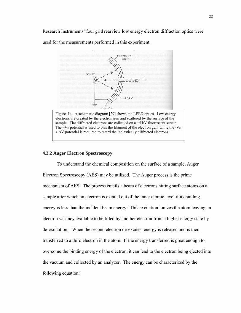
Research Instruments’ four grid rearview low energy electron diffraction optics were
used for the measurements performed in this experiment.
Figure. 14. A schematic diagram [29] shows the LEED optics. Low energy electrons are created by the electron gun and scattered by the surface of the sample. The diffracted electrons are collected on a +5 kV fluorescent screen. The –VE potential is used to bias the filament of the electron gun, while the -VE + ∆V potential is required to retard the inelastically diffracted electrons.
4.3.2 Auger Electron Spectroscopy
To understand the chemical composition on the surface of a sample, Auger
Electron Spectroscopy (AES) may be utilized. The Auger process is the prime
mechanism of AES. The process entails a beam of electrons hitting surface atoms on a
sample after which an electron is excited out of the inner atomic level if its binding
energy is less than the incident beam energy. This excitation ionizes the atom leaving an
electron vacancy available to be filled by another electron from a higher energy state by
de-excitation. When the second electron de-excites, energy is released and is then
transferred to a third electron in the atom. If the energy transferred is great enough to
overcome the binding energy of the electron, it can lead to the electron being ejected into
the vacuum and collected by an analyzer. The energy can be characterized by the
following equation:
23
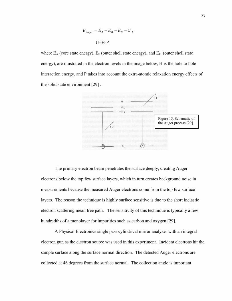
UEEEE CBAAuger −−−= ,
U=H-P
where EA (core state energy), EB (outer shell state energy), and EC (outer shell state
energy), are illustrated in the electron levels in the image below, H is the hole to hole
interaction energy, and P takes into account the extra-atomic relaxation energy effects of
the solid state environment [29] .
The primary electron beam penetrates the surface deepl
electrons below the top few surface layers, which in turn create
measurements because the measured Auger electrons come from
layers. The reason the technique is highly surface sensitive is d
electron scattering mean free path. The sensitivity of this techn
hundredths of a monolayer for impurities such as carbon and ox
A Physical Electronics single pass cylindrical mirror an
electron gun as the electron source was used in this experiment
sample surface along the surface normal direction. The detecte
collected at 46 degrees from the surface normal. The collection
Figure 15. Schematic of the Auger process [29].
y, creating Auger
s background noise in
the top few surface
ue to the short inelastic
ique is typically a few
ygen [29].
alyzer with an integral
. Incident electrons hit the
d Auger electrons are
angle is important
24
because it reduces the effective escape depth of the Auger electrons by a factor of cos(46
degrees).
Auger spectra are typically used for qualitative identification of surface species.
If the elemental sensitivity factors are known it is possible to quantitatively determine the
amount of a present surface species. By comparing the peak height intensities from two
separate Auger spectra, an estimate of the relative concentration of a surface species
(cobalt) can be determined.
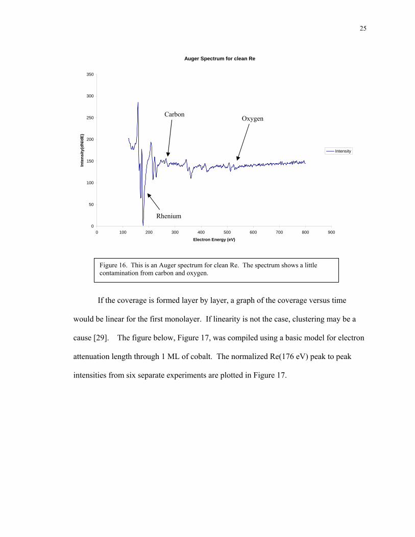
By assuming 1ML of cobalt covers the Re surface, the following formula can be
used to give a rough estimate of coverage:
IRe/IRe Clean= exp(-dCo/λRe)=0.49,
Intensity I176E
Co)for A (2.5 atom ofdiameter d)5.3(path freemean inelastic
Re
Re
==
===
eV
Aλλ
where I is the peak intensity at ERe, d is the diameter of a Co atom, and λRe is the
attenuation length through the Co. From Figure 17, this peak ratio corresponds to
approximately 5 +/- 1 minute to cover the surface in 1ML.
25
Auger Spectrum for clean Re
0
50
100
150
200
250
300
350
0 100 200 300 400 500 600 700 800 900
Electron Energy (eV)
Inte
nsity
(dN
/dE)
Intensity
n Oxygen
would
cause [
attenua
intensi
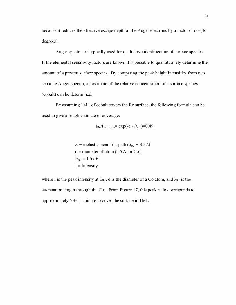
Figure 16. This is an Auger spectrum for clean Re. The spectrum shows a littlecontamination from carbon and oxygen.
If the coverage is
be linear for the f
29]. The figure
tion length throug
ties from six sepa
Rhenium
fo
irs
be
h
rat
Carbo
rmed layer by layer, a graph of the coverage versus time
t monolayer. If linearity is not the case, clustering may be a
low, Figure 17, was compiled using a basic model for electron
1 ML of cobalt. The normalized Re(176 eV) peak to peak
e experiments are plotted in Figure 17.
26
Normalized Intensity versus Time
0
0.2
0.4
0.6
0.8
1
1.2
0 2 4 6 8 10 12 14
Time (min)
Nor
mal
ized
Inte
nsity
Re Data1ML
~0.49 or 1ML
~5 min
4.3.3 Sc
A
the majo
morphol
objects a
probe th
A
electrica
moves li
between
Figure 17. This graph was created by estimating the electron attenuation length for 1ML of Co on Re(11-21). From this graph estimates of cobalt coverage are made for the entire paper.
anning Tunneling Microscopy
McAllister UHV Scanning Tunneling Microscope (STM) was used to acquire
rity of data in this study. The STM allows a user to access real-space
ogy of solid surfaces with atomic resolution. It can be used to create nanoscale
s well as manipulate individual atoms. In this study, the STM was used to
e rhenium surface for cobalt.
n optically sharp tip is mounted such that it can be manipulated via an
lly controlled piezo material to move in the X, Y, and Z directions. The tip
ne by line across the surface, scanning it. The scanning records the differences
local electronic states. The electronic states are explored using a quantum
27
tunneling current (1 nA) between the tip and the neighboring region of the surface; a bias
voltage (1V) spans the gap in between [29].
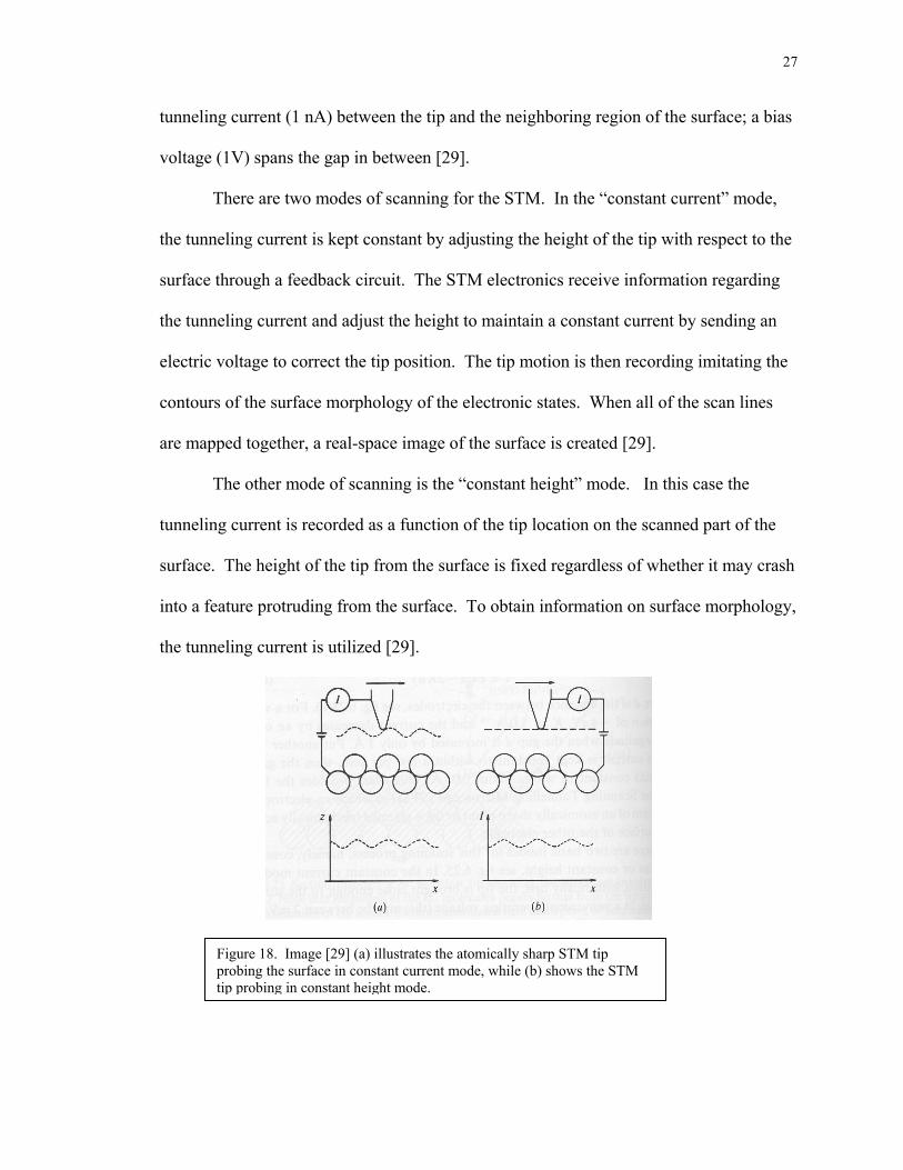
There are two modes of scanning for the STM. In the “constant current” mode,
the tunneling current is kept constant by adjusting the height of the tip with respect to the
surface through a feedback circuit. The STM electronics receive information regarding
the tunneling current and adjust the height to maintain a constant current by sending an
electric voltage to correct the tip position. The tip motion is then recording imitating the
contours of the surface morphology of the electronic states. When all of the scan lines
are mapped together, a real-space image of the surface is created [29].
The other mode of scanning is the “constant height” mode. In this case the
tunneling current is recorded as a function of the tip location on the scanned part of the
surface. The height of the tip from the surface is fixed regardless of whether it may crash
into a feature protruding from the surface. To obtain information on surface morphology,
the tunneling current is utilized [29].
Figure 18. Image [29] (a) illustrates the atomically sharp STM tip probing the surface in constant current mode, while (b) shows the STM tip probing in constant height mode.
28
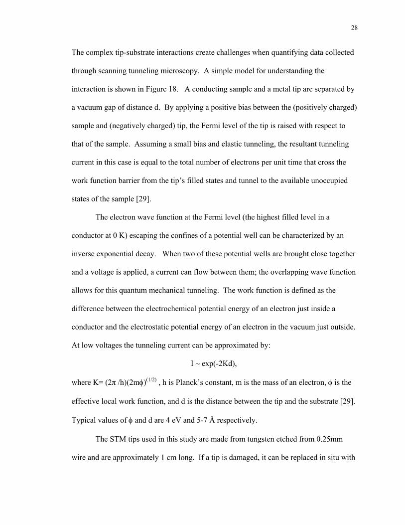
The complex tip-substrate interactions create challenges when quantifying data collected
through scanning tunneling microscopy. A simple model for understanding the
interaction is shown in Figure 18. A conducting sample and a metal tip are separated by
a vacuum gap of distance d. By applying a positive bias between the (positively charged)
sample and (negatively charged) tip, the Fermi level of the tip is raised with respect to
that of the sample. Assuming a small bias and elastic tunneling, the resultant tunneling
current in this case is equal to the total number of electrons per unit time that cross the
work function barrier from the tip’s filled states and tunnel to the available unoccupied
states of the sample [29].
The electron wave function at the Fermi level (the highest filled level in a
conductor at 0 K) escaping the confines of a potential well can be characterized by an
inverse exponential decay. When two of these potential wells are brought close together
and a voltage is applied, a current can flow between them; the overlapping wave function
allows for this quantum mechanical tunneling. The work function is defined as the
difference between the electrochemical potential energy of an electron just inside a
conductor and the electrostatic potential energy of an electron in the vacuum just outside.
At low voltages the tunneling current can be approximated by:
I ~ exp(-2Kd),
where K= (2π /h)(2mφ)(1/2) , h is Planck’s constant, m is the mass of an electron, φ is the
effective local work function, and d is the distance between the tip and the substrate [29].
Typical values of φ and d are 4 eV and 5-7 Å respectively.
The STM tips used in this study are made from tungsten etched from 0.25mm
wire and are approximately 1 cm long. If a tip is damaged, it can be replaced in situ with
29
a wobble-stick designed specifically for tip changing. The tips used for this experiment
were purchased from Custom Probes Unlimited.
Figure 12 illustrates the McAllister UHV STM with the sample holder assembly
on the conducting rails. Before measurements can be made, the STM device must be
isolated from vibrations. To accomplish this task, the STM platform is detached from the
base plate by unscrewing the clamp. This leaves the entire STM platform supported by
four springs to provide dampening from interfering vibrations. Due to the size of the gap
between the tip and surface, isolation from any vibrations is imperative. If vibrations
occur during measurement, the results can range from invalid data to surface destruction
due to the tip crashing into the surface [29].
After the platform is isolated, the sample holder assembly is moved along the
conduction rails. An optical microscope is then used to finely adjust the location of the
sample holder, guiding the final stage of the motion. A programmed sequence of tip and
sample movements is used to establish a tunneling current.
During the scanning process (sometimes before scanning can begin), the tip
becomes dirty. The software provided with the STM has a “bias pulse” function and is
used for cleaning dirty tips. A pulsed bias can be applied to the tip-surface in junction
with a preset voltage between -10 V and +10 V. (Obviously, this technique can lead to
surface degradation and should be performed near an isolated area of the surface.)
Another method for cleaning the tip comes from scanning a non-interesting part of the
surface very quickly. This rough treatment of the tip is designed to drop extra atoms
from the tip or pick up adatoms from the surface in hope of creating an atomically sharp
tip.
30
Despite problems with tip cleanliness, chamber vibrations, and establishment of a
tunneling current, the McAllister UHV STM is a very powerful tool for surface
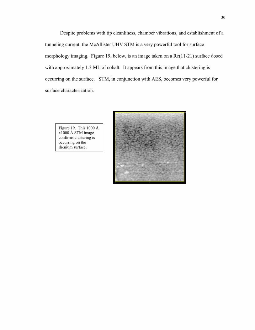
morphology imaging. Figure 19, below, is an image taken on a Re(11-21) surface dosed
with approximately 1.3 ML of cobalt. It appears from this image that clustering is
occurring on the surface. STM, in conjunction with AES, becomes very powerful for
surface characterization.
Figure 19. This 1000 Å x1000 Å STM image confirms clustering is occurring on the rhenium surface.
31
Chapter 5
Oxygen Induced Faceting of Rhenium(123 1)
A myriad of experiments have been conducted driven by the desire to understand
the nature of adsorbates, substrates, and surface free energy. If the anisotropy of the
surface free energy is enhanced by adsorbates covering the substrate’s surface and
annealing, facets may form minimizing the total free surface energy. The process of
forming facets in this manner is thermodynamically driven, involving mass transport of
immense quantities of atoms. The size and shape of the facets is determined by
nucleation rates and diffusion rates [28].
Surface free energy,γ, is defined as the reversible work necessary to create a
surface, and is expressed as energy per area. For a solid the surface free energy is
proportional to the cleavage energy and is roughly the energy necessary to break surface
bonds. A typical surface free energy for a solid is approximately 1200 ergs/cm2 or 1.2
J/m2. The equilibrium shape of small crystals can be determined from anisotropy in
surface free energy. The crystal will seek a shape that minimizes the integral:
at constant volume: this is Wulff’s theorem [32].
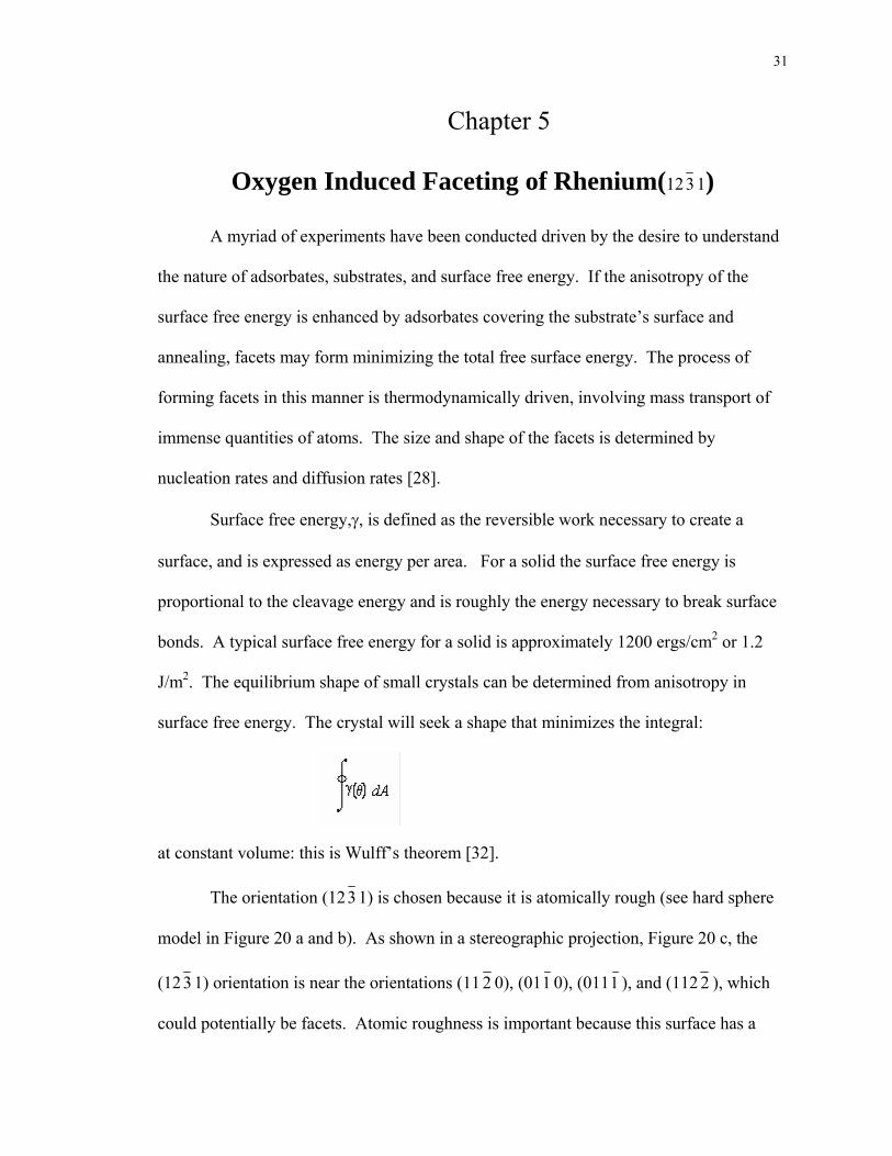
The orientation (123 1) is chosen because it is atomically rough (see hard sphere
model in Figure 20 a and b). As shown in a stereographic projection, Figure 20 c, the
(123 1) orientation is near the orientations (11 2 0), (011 0), (0111 ), and (112 2 ), which
could potentially be facets. Atomic roughness is important because this surface has a
32
greater surface free energy than more close-packed Re surfaces. Clean planar rhenium
does not form facets spontaneously. Oxygen is necessary to increase the anisotropy of
the surface free energy, as discussed in more detail in the following pages [21,27].
Rhenium has a hexagonal close packed structure with unit cell parameters a=2.716 Å and
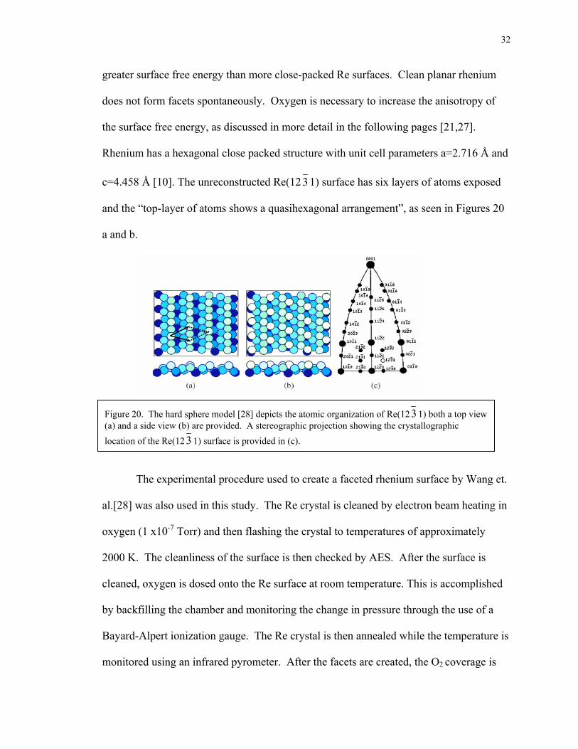
c=4.458 Å [10]. The unreconstructed Re(123 1) surface has six layers of atoms exposed
and the “top-layer of atoms shows a quasihexagonal arrangement”, as seen in Figures 20
a and b.
Figure 20. The hard sphere model [28] depicts the atomic organization of Re(123 1) both a top view (a) and a side view (b) are provided. A stereographic projection showing the crystallographic location of the Re(12 3 1) surface is provided in (c).
The experimental procedure used to create a faceted rhenium surface by Wang et.
al.[28] was also used in this study. The Re crystal is cleaned by electron beam heating in
oxygen (1 x10⁻⁷ Torr) and then flashing the crystal to temperatures of approximately
2000 K. The cleanliness of the surface is then checked by AES. After the surface is
cleaned, oxygen is dosed onto the Re surface at room temperature. This is accomplished
by backfilling the chamber and monitoring the change in pressure through the use of a
Bayard-Alpert ionization gauge. The Re crystal is then annealed while the temperature is
monitored using an infrared pyrometer. After the facets are created, the O2 coverage is
33
confirmed by AES measurements and the facets are confirmed by LEED. Next,
extensive STM scans are performed [28]. Other surfaces such as W(111), Mo(111), and
Ir(210) have been shown to have ridge like morphology under absorbate-induced faceting
conditions [5,15,18]. In particular, W(111), a body centered cubic, has been the most
carefully studied [14,15].
The procedure mentioned above is one way to create a faceted surface. The
largest facets used in this experiment were generated by three or four, ten second
sequential e-beam heatings to temperatures greater than 2200K of Re(123 1), followed by
cooling in O2 at a pressure of 1x10⁻⁷ Torr. Further detail is provided in chapter 6
regarding the experimental procedure used to create the faceted surfaces used in this
experiment.
By using the methods discussed in Chapter 4, the O/Re Auger peaks are used to
determine the coverage of the oxygen. The amount of oxygen dosed is measured in
Langmuirs, L, where 1L=1x10⁻⁶ Torr *s=1.33x10⁻⁴ Pa*s. Oxygen saturates the surface
between 5 and 7L or approximately 1 ML (1ML= 1x10¹⁵ atoms/cm2). After AES is used
to confirm the oxygen coverage, LEED is performed to confirm the faceting [28].
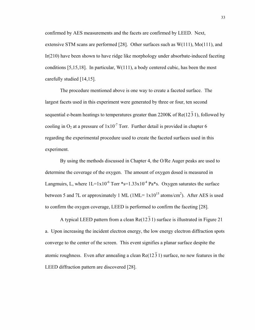
A typical LEED pattern from a clean Re(123 1) surface is illustrated in Figure 21
a. Upon increasing the incident electron energy, the low energy electron diffraction spots
converge to the center of the screen. This event signifies a planar surface despite the
atomic roughness. Even after annealing a clean Re(123 1) surface, no new features in the
LEED diffraction pattern are discovered [28].
34
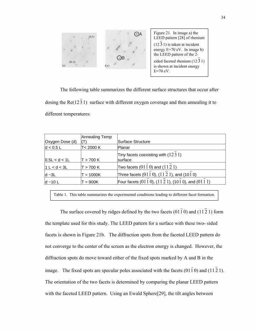
The following table summarizes the different
dosing the Re(123 1) surface with different oxygen c
different temperatures:
Oxygen Dose (d) Annealing Temp (T) Surface Structure
d < 0.5 L T< 2000 K Planar
0.5L < d < 1L T > 700 K Tiny facets coexistsurface
1 L < d < 3L T > 700 K Two facets (011 0d ~3L T = 1000K Three facets (011d ~10 L T = 900K Four facets (011 0
Table 1. This table summarizes the experimental condition
The surface covered by ridges defined by the
the template used for this study. The LEED pattern fo
facets is shown in Figure 21b. The diffraction spots
not converge to the center of the screen as the electro
diffraction spots do move toward either of the fixed s
image. The fixed spots are specular poles associated
The orientation of the two facets is determined by com
with the faceted LEED pattern. Using an Ewald Sphe
Figure 21. In image a) the LEED pattern [28] of rhenium (12 3 1) is taken at incident energy E=70 eV. In image b) the LEED pattern of the 2-sided faceted rhenium (12 3 1) is shown at incident energy E=70 eV.
surface structures that occur after
overage and then annealing it to
ing with (123 1)
) and (11 2 1)
0), (11 2 1), and (101 0)
), (11 2 1), (101 0), and (011 1)
s leading to different facet formation.
two facets (011 0) and (11 2 1) form
r a surface with these two- sided
from the faceted LEED pattern do
n energy is changed. However, the
pots marked by A and B in the
with the facets (011 0) and (11 2 1).
paring the planar LEED pattern
re[29], the tilt angles between
35
spectral poles associated with A and B taken with respect to the Re(123 1) norm can be
calculated. The angles were determined to by 22.2 degrees and 12.0 degrees. Based on
these measurements and calculations the Miller Indices of the facets were identified [28].
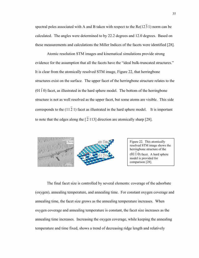
Atomic resolution STM images and kinematical simulations provide strong
evidence for the assumption that all the facets have the “ideal bulk-truncated structures.”
It is clear from the atomically resolved STM image, Figure 22, that herringbone
structures exist on the surface. The upper facet of the herringbone structure relates to the
(011 0) facet, as illustrated in the hard sphere model. The bottom of the herringbone
structure is not as well resolved as the upper facet, but some atoms are visible. This side
corresponds to the (11 2 1) facet as illustrated in the hard sphere model. It is important
to note that the edges along the [ 2 113] direction are atomically sharp [28].
Figure 22. This atomically resolved STM image shows the herringbone structure of the (011 0) facet. A hard sphere model is provided for comparison [28].
The final facet size is controlled by several elements: coverage of the adsorbate
(oxygen), annealing temperature, and annealing time. For constant oxygen coverage and
annealing time, the facet size grows as the annealing temperature increases. When
oxygen coverage and annealing temperature is constant, the facet size increases as the
annealing time increases. Increasing the oxygen coverage, while keeping the annealing
temperature and time fixed, shows a trend of decreasing ridge length and relatively
36
constant ridge width. Typical ridge length varies from 50 Å to 450 Å and typical ridge
width varies from 10 Å to 200 Å. The ridges have been observed to last up to a week
without morphological changes [28].
Thermodynamics and kinetics are the general causes of faceting. The primary
driving force for surface faceting is an anisotropy of the surface free energy. In order for
facets to form, all the thermally stable facets must be present and the faceted surface’s
total free energy must be smaller than the total surface free energy of the original planar
surface [11]. In the case of clean metal surfaces, the anisotropy of the surface free energy
is not great enough when annealed to cause faceting [4,13]. By covering a metal planar
surface with an adsorbate, the surface free energy is generally decreased and may, upon
annealing, cause faceting. The energetic requirements for faceting of Re(123 1), ignoring
edge energies, are calculated by:
“where θi is the tilt angle between facet i and the (123 1) plane, λi is the
structural coefficient describing the partial contribution of facet i to the total projected
area on (123 1) by all the facets, and γi is the surface free energy of facet i per unit area
[28].” From the equation above, it can be determined that the facets that have the
smallest surface free energy of facet per unit area and tilt angle are more favorable and
thus likely to form [1,24,27,31].
In summary: adsorption of oxygen on Re(123 1), followed by annealing to an
elevated temperature, induces morphological changes. Different oxygen coverage leads
to different facet formation. For 1L to 3 L of dosed oxygen and annealing to

37
temperatures less than 700K, the surface becomes completely faceted with (011 0) and
(11 2 1) facets. The distance between facets, or facet width, is relatively uniform and the
edges are atomically sharp [28].
38
Chapter 6
Preferential Nucleation of Co Nanoclusters on Re(123 1)
6.1 Introduction
The initial goal of this study was to discover the conditions under which cobalt
nanowires would nucleate on the faceted O/Re(123 1) surface. However, by annealing
the cobalt after deposition, nanoclusters were observed. In order to guarantee that all
experiments were performed under well defined conditions, the surface cleanliness and
coverage were monitored by AES.
6.2 Cleaning
Cleanliness is important when studying the physical and electronic properties of a
surface. In order to ensure a clean surface is used for each experiment, the cleaning
procedure in chapter 4 is followed. The typical electron bombardment conditions for
flash heating the sample are a voltage of 2.0 kV, a current of 100 mA, for a duration of 15
seconds.
6.3 Experimental Results
Four different experiments were performed that achieved scientifically interesting
results. The first two experiments showed that Co nanoclusters preferentially nucleate in
the trenches of the faceted Re(123 1) surface. The third and fourth experiments showed
that the Co nanoclusters could be controlled in size, while still preferentially nucleating in
the trenches of the faceted Re(123 1) surface. The table below summarizes the
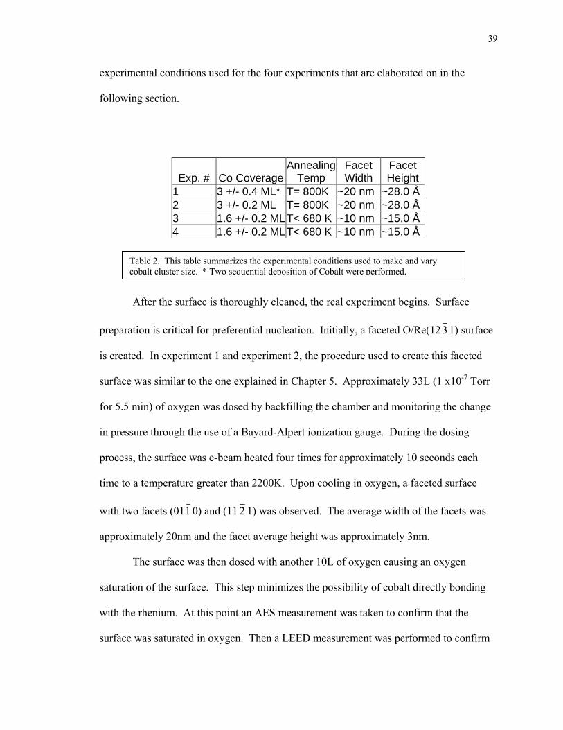
39
experimental conditions used for the four experiments that are elaborated on in the
following section.
Exp. # Co CoverageAnnealing
Temp Facet Width
Facet Height
1 3 +/- 0.4 ML* T= 800K ~20 nm ~28.0 Å 2 3 +/- 0.2 ML T= 800K ~20 nm ~28.0 Å 3 1.6 +/- 0.2 MLT< 680 K ~10 nm ~15.0 Å 4 1.6 +/- 0.2 MLT< 680 K ~10 nm ~15.0 Å
prepa
is crea
surfac
for 5.
in pre
proce
time t
with t
appro
satura
with t
surfac
Table 2. This table summarizes the experimental conditions used to make and vary cobalt cluster size. * Two sequential deposition of Cobalt were performed.
After the surface is thoroughly cleaned, the real experiment begins. Surface
ration is critical for preferential nucleation. Initially, a faceted O/Re(123 1) surface
ted. In experiment 1 and experiment 2, the procedure used to create this faceted
e was similar to the one explained in Chapter 5. Approximately 33L (1 x10⁻⁷ Torr
5 min) of oxygen was dosed by backfilling the chamber and monitoring the change
ssure through the use of a Bayard-Alpert ionization gauge. During the dosing
ss, the surface was e-beam heated four times for approximately 10 seconds each
o a temperature greater than 2200K. Upon cooling in oxygen, a faceted surface
wo facets (011 0) and (11 2 1) was observed. The average width of the facets was
ximately 20nm and the facet average height was approximately 3nm.
The surface was then dosed with another 10L of oxygen causing an oxygen
tion of the surface. This step minimizes the possibility of cobalt directly bonding
he rhenium. At this point an AES measurement was taken to confirm that the
e was saturated in oxygen. Then a LEED measurement was performed to confirm
40
the surface was properly faceted. In experiment 1, two sequential dosings of cobalt were
performed. The first cobalt dosing provided 1 ML +/- 0.2 ML of cobalt and the second
dosing provided 2 ML +/- 0.2 ML of cobalt coverage. The total cobalt coverage was
approximately 3.0 ML. AES and LEED measurements were performed again to confirm
the cobalt coverage and that the facets still remained. Finally, the Co/O/Re(123 1)
faceted surface was gently annealed to a temperature of approximately 800K for 3
minutes.
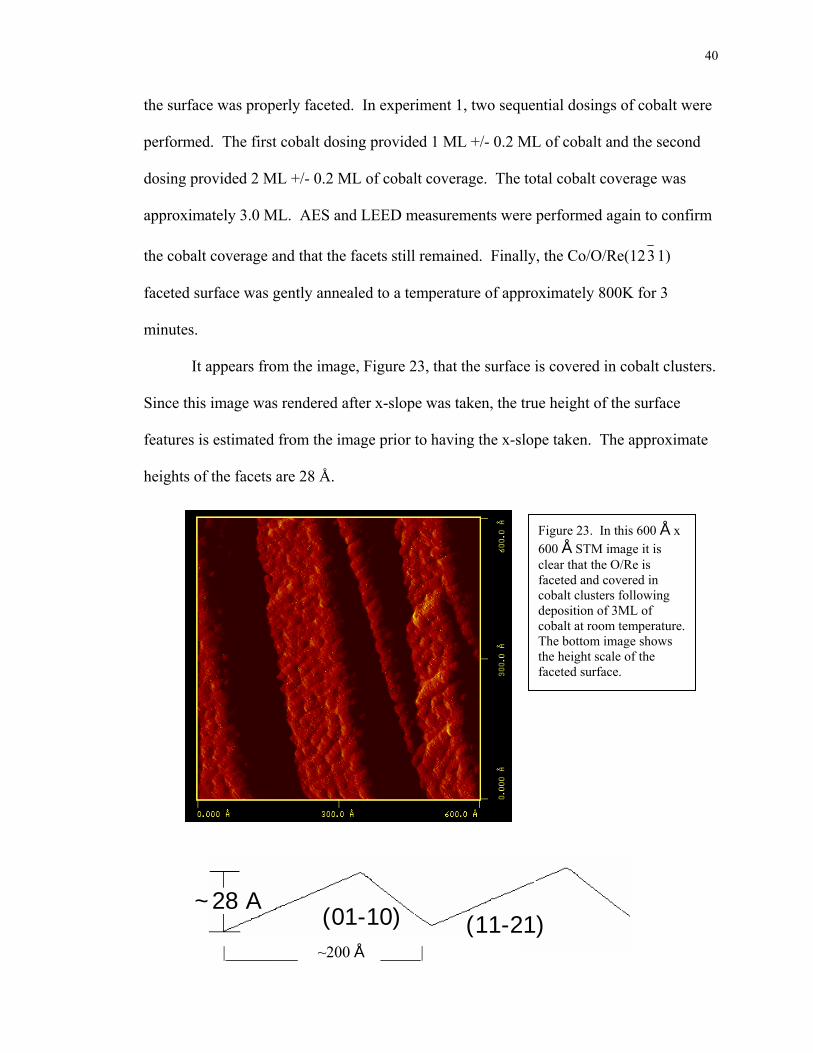
It appears from the image, Figure 23, that the surface is covered in cobalt clusters.
Since this image was rendered after x-slope was taken, the true height of the surface
features is estimated from the image prior to having the x-slope taken. The approximate
heights of the facets are 28 Å.
(01-10) (11-21 |_________ ~200 Å _____|
~28 A
Figure 23. In this 600 Å x 600 Å STM image it is clear that the O/Re is faceted and covered in cobalt clusters following deposition of 3ML of cobalt at room temperature. The bottom image shows the height scale of the faceted surface.
)
41
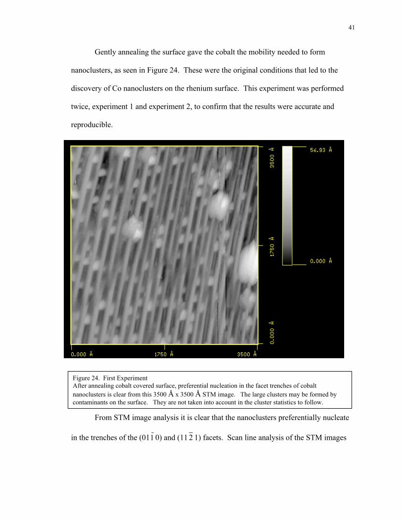
Gently annealing the surface gave the cobalt the mobility needed to form
nanoclusters, as seen in Figure 24. These were the original conditions that led to the
discovery of Co nanoclusters on the rhenium surface. This experiment was performed
twice, experiment 1 and experiment 2, to confirm that the results were accurate and
reproducible.
Figure 24. First Experiment After annealing cobalt covered surface, preferential nucleation in the facet trenches of cobalt nanoclusters is clear from this 3500 Å x 3500 Å STM image. The large clusters may be formed by contaminants on the surface. They are not taken into account in the cluster statistics to follow.
From STM image analysis it is clear that the nanoclusters preferentially nucleate
in the trenches of the (011 0) and (11 2 1) facets. Scan line analysis of the STM images
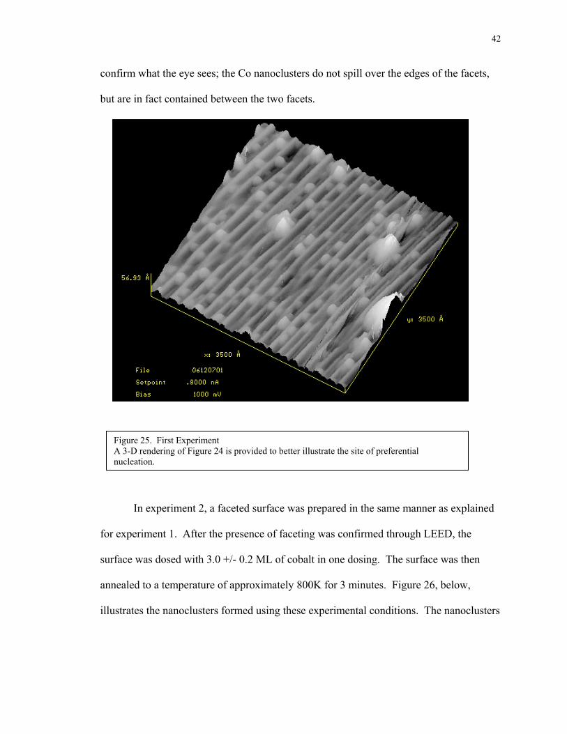
42
confirm what the eye sees; the Co nanoclusters do not spill over the edges of the facets,
but are in fact contained between the two facets.
Figure 25. First Experiment A 3-D rendering of Figure 24 is provided to better illustrate the site of preferential nucleation.
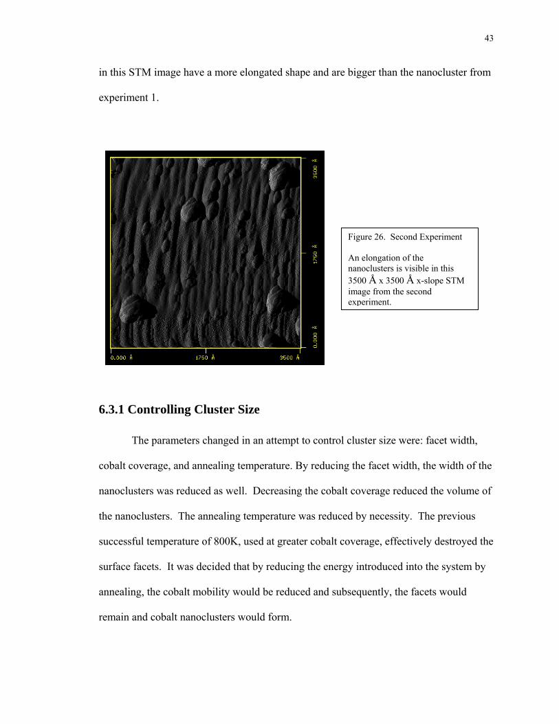
In experiment 2, a faceted surface was prepared in the same manner as explained
for experiment 1. After the presence of faceting was confirmed through LEED, the
surface was dosed with 3.0 +/- 0.2 ML of cobalt in one dosing. The surface was then
annealed to a temperature of approximately 800K for 3 minutes. Figure 26, below,
illustrates the nanoclusters formed using these experimental conditions. The nanoclusters
43
in this STM image have a more elongated shape and are bigger than the nanocluster from
experiment 1.
Figure 26. Second Experiment An elongation of the nanoclusters is visible in this 3500 Å x 3500 Å x-slope STM image from the second experiment.
6.3.1 Controlling Cluster Size
The parameters changed in an attempt to control cluster size were: facet width,
cobalt coverage, and annealing temperature. By reducing the facet width, the width of the
nanoclusters was reduced as well. Decreasing the cobalt coverage reduced the volume of
the nanoclusters. The annealing temperature was reduced by necessity. The previous
successful temperature of 800K, used at greater cobalt coverage, effectively destroyed the
surface facets. It was decided that by reducing the energy introduced into the system by
annealing, the cobalt mobility would be reduced and subsequently, the facets would
remain and cobalt nanoclusters would form.
44
In experiments 3 and 4, the surface was thoroughly cleaned before the faceted
surface was prepared. A faceted O/Re(123 1) surface was again created, but this time the
parameters were varied slightly to diminish the width of the facets. The procedure of e-
beam heating was followed, however, approximately 24L (1 x10⁻⁷ Torr for 4 min) of
oxygen was dosed by backfilling the chamber and monitoring the change in pressure
through the use of a Bayard-Alpert ionization gauge. During the dosing process, the
surface was e-beam heated three times for approximately 10 seconds each time to a
temperature greater than 2200K. Cooling in oxygen created a faceted surface with two
facets, (011 0) and (11 2 1). The average width of the facets was approximately 10nm
and the facet average height was approximately 2nm.
The surface was then further dosed with another 10L of oxygen causing oxygen
saturation. An AES measurement was taken to confirm oxygen surface saturation,
followed by a LEED measurement to confirm the surface was properly faceted. The next
step was to dose the cobalt, but for about half the time. This provided 1.6 +/- 0.2 ML
coverage of cobalt on the surface. AES and LEED measurements were performed again
to confirm the cobalt coverage and faceting. Finally, the Co/O/Re(123 1) faceted surface
was gently annealed to a temperature less than 680K +/- 30K for 3 minutes. Using these
conditions, the size of the cobalt clusters varied. This experiment was performed twice,
experiments 3 and 4, to confirm that the results were accurate and reproducible.
45
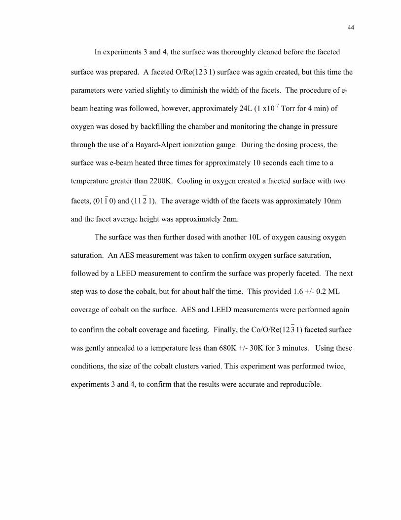
Figure 27. Third Experiment This 2000 Å x 3500 Å x-slope STM image shows a reduction in facet size as well as cluster size in comparison to Figures 24 and 26. The large formation in the center of the image is anomalous to the surface.
The third experiment’s (experiment 3), facet size is approximately 19 Å in height
and 95 Å in width. From the image above, Figure 27, it is clear that the facets are smaller
in width than those of experiment 1 and 2; also the Co clusters also decrease in size. It is
clear from the x-slope of the STM image, Figure 27, that nanoclusters preferentially
nucleate in the trenches of the (011 0) and (11 2 1) facets. Again, using scan line analysis
(see section 6.4, below) it was confirmed that the clusters remain between the facets.
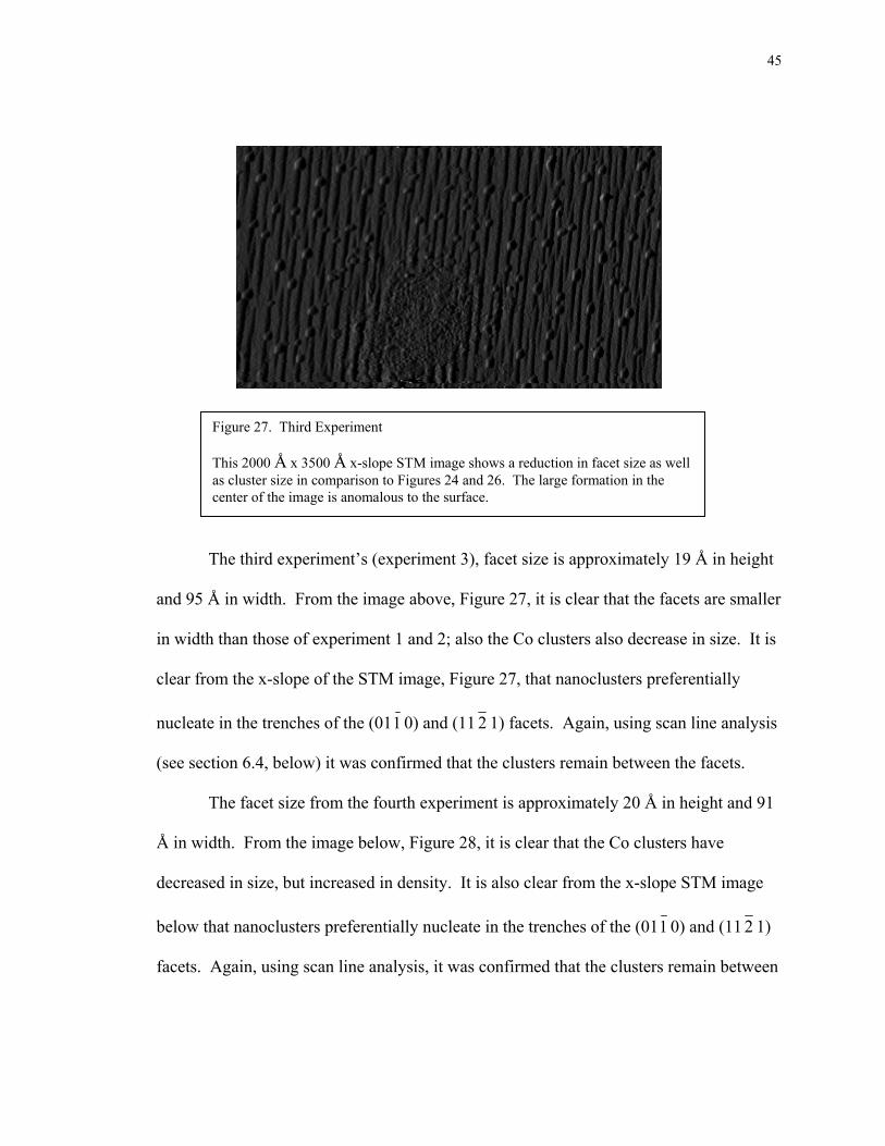
The facet size from the fourth experiment is approximately 20 Å in height and 91
Å in width. From the image below, Figure 28, it is clear that the Co clusters have
decreased in size, but increased in density. It is also clear from the x-slope STM image
below that nanoclusters preferentially nucleate in the trenches of the (011 0) and (11 2 1)
facets. Again, using scan line analysis, it was confirmed that the clusters remain between
46
the facets. Statistical analysis of the nanoclusters for all experiments is provided in the
following section.
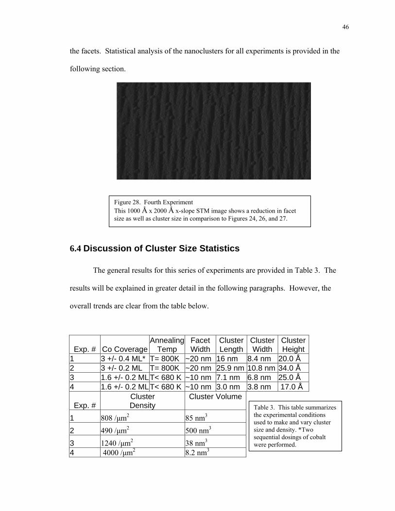
6.4 Discus
The g
results will be
overall trends
Exp. # Co1 3 +2 3 +3 1.64 1.6
Exp. # 1 8082 4903 1244 40
Figure 28. Fourth Experiment This 1000 Å x 2000 Å x-slope STM image shows a reduction in facetsize as well as cluster size in comparison to Figures 24, 26, and 27.
sion of Cluster Size Statistics
eneral results for this series of experiments are provided in Table 3. The
explained in greater detail in the following paragraphs. However, the
are clear from the table below.
Coverage Annealing
Temp Facet Width
ClusterLength
ClusterWidth
Cluster Height
/- 0.4 ML* T= 800K ~20 nm 16 nm 8.4 nm 20.0 Å /- 0.2 ML T= 800K ~20 nm 25.9 nm 10.8 nm 34.0 Å +/- 0.2 ML T< 680 K ~10 nm 7.1 nm 6.8 nm 25.0 Å +/- 0.2 ML T< 680 K ~10 nm 3.0 nm 3.8 nm 17.0 Å
Cluster Density
Cluster Volume
/µm2 85 nm3
/µm2 500 nm3 0 /µm2 38 nm3
00 /µm2 8.2 nm3
Table 3. This table summarizes the experimental conditions used to make and vary cluster size and density. *Two sequential dosings of cobalt were performed.
47
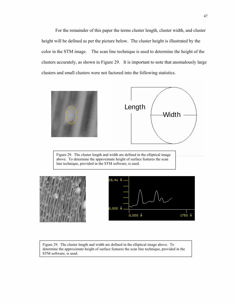
For the remainder of this paper the terms cluster length, cluster width, and cluster
height will be defined as per the picture below. The cluster height is illustrated by the
color in the STM image. The scan line technique is used to determine the height of the
clusters accurately, as shown in Figure 29. It is important to note that anomalously large
clusters and small clusters were not factored into the following statistics.
WidthLength
Figure 29. The cluster length and width are defined in the elliptical image above. To determine the approximate height of surface features the scan line technique, provided in the STM software, is used.
Figure 29. The cluster length and width are defined in the elliptical image above. To determine the approximate height of surface features the scan line technique, provided in the STM software, is used.
48
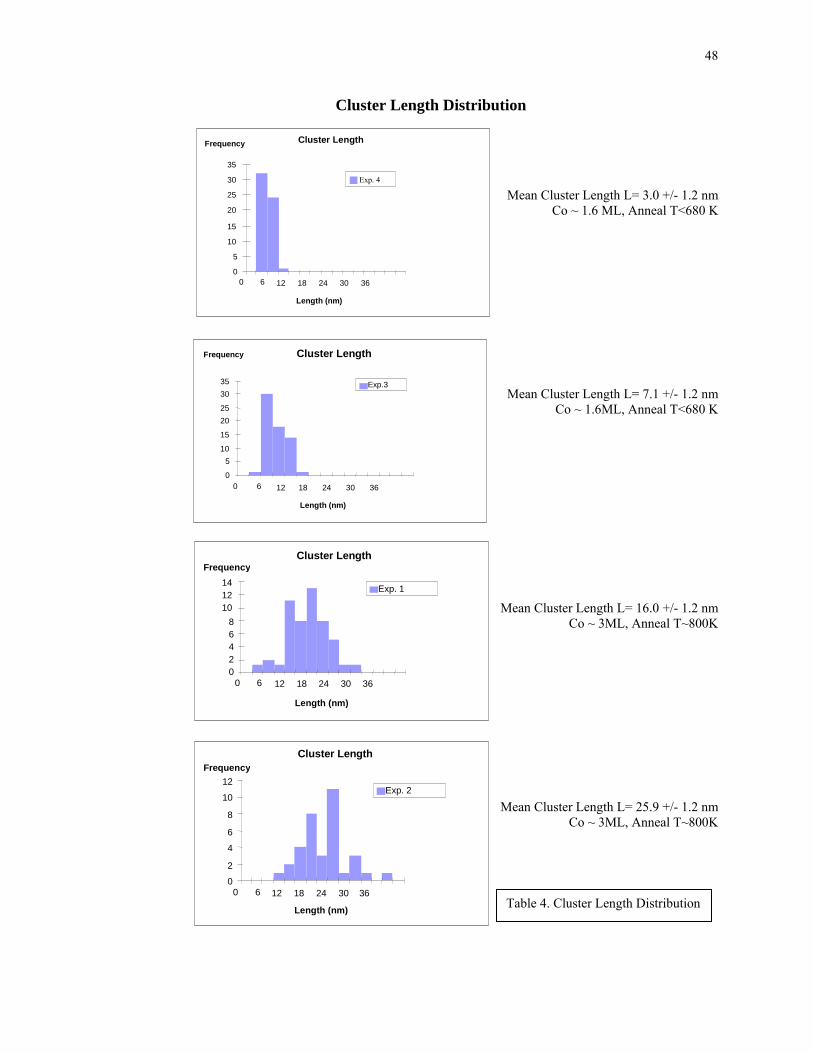
Cluster Length Distribution
Mean Cluster Length L= 3.0 +/- 1.2 nm
Co ~ 1.6 ML, Anneal T<680 K
Cluster Length
0 5
10 15 20 25 30 35
0 6 12 18 24 30 36
Length (nm)
Frequency
Exp. 4
Mean Cluster Length L= 7.1 +/- 1.2 nm Co ~ 1.6ML, Anneal T<680 K
Cluster Length
0 5
10 15 20 25 30 35
0 6 12 18 24 30 36
Length (nm)
Frequency
Ex
p.3
Mean Cluster Length L= 16.0 +/- 1.2 nm Co ~ 3ML, Anneal T~800K
Cluster Length
0 2 4 6 8
10
12 14
0 6 12 18 24 30 36
Length (nm)
Frequency Exp. 1
Mean Cluster Length L= 25.9 +/- 1.2 nm Co ~ 3ML, Anneal T~800K
Cluster Length
0 2 4 6 8
10 12
0 6 12 18 24 30 36
Length (nm)
Frequency Exp. 2
Table 4. Cluster Length Distribution
49
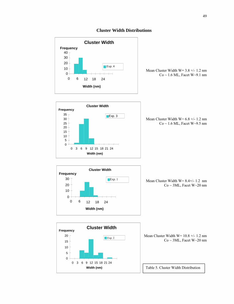
Cluster Width Distributions
Mean Cluster Width W= 3.8 +/- 1.2 nm Co ~ 1.6 ML, Facet W~9.1 nm
Cluster Width
Mean Cluster Width W= 6.8 +/- 1.2 nm Co ~ 1.6 ML, Facet W~9.5 nm
Mean Cluster Width W= 8.4+/- 1.2 nm Co ~ 3ML, Facet W~20 nm
Mean Cluster Width W= 10.8 +/- 1.2 nm Co ~ 3ML, Facet W~20 nm
0
20 30 40
0 6 12 18 24
Width (nm)
Frequency
10Exp. 4
Cluster Width
0 5
10 15 20 25 30 35
0 3 6 9 12 15 18 21 24Width (nm)
Frequency Exp. 3
Cluster Width
0 10 20 30
0 6 12 18 24
Width (nm)
Frequency Exp. 1
Cluster Width
0 5
10 15
0 3 6 9 12 15 18 21 24Width (nm)
Frequency 20
Exp. 2
Table 5. Cluster Width Distribution
50
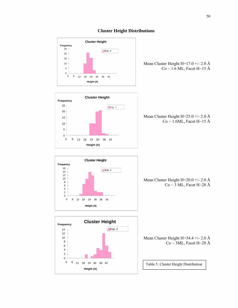
Cluster Height Distributions
Mean Cluster Height H=17.0 +/- 2.0 Å Co ~ 1.6 ML, Facet H~15 Å
Cluster Height
0 5
10 15 20 25
0 6 12 18 24 30 36 42
Height (A)
Frequency Exp. 4
Mean Cluster Height H=25.0 +/- 2.0 Å Co ~ 1.6ML, Facet H~15 Å
Cluster Height
0 5
10 15 20 25
0 6 12 18 24 30 36 42
Height (A)
Frequency Exp. 3
Mean Cluster Height H=20.0 +/- 2.0 Å Co ~ 3 ML, Facet H~28 Å
Cluster Height
0 2 4 6 8
10
12 14 16
0 6 12 18 24 30 36 42
Height (A)
Frequency Exp. 1
Mean Cluster Height H=34.4 +/- 2.0 Å Co ~ 3ML, Facet H~28 Å
Cluster Height
0 2 4 6 8
10 12 14
0 6 12 18 24 30 36 42
Height (A)
FrequencyExp. 2
Table 5. Cluster Height Distribution
51
The cluster length varied from experiment 1 to experiment 2. The mean length
for experiment 1 is 16.0 +/- 1.2 nm and for experiment 2 is 25.9 +/- 1.2 nm. From STM
images, it is clear that the clusters in experiment 2 are elongated.
Both experiments 1 and 2 showed similar mean cluster widths. Experiment 1’s
mean cluster width is 8.4 +/- 1.2 nm, while experiment 2’s mean cluster width is 10.8 +/-
1.2 nm. This means that in both cases, the nanoclusters are contained between the facets.
The cluster height varies significantly between the experiments 1 and 2.
Experiment 1’s mean height is 20.0 +/- 2.0 Å, while the mean height is 34.0 +/- 2.0 Å for
experiment 2. This means that experiment 1’s mean height is less than the facet height,
while the mean cluster height is taller than the facets in experiment 2.
The cluster density may shed some light on the variations between the cluster
length, width, and height between experiments 1 and 2. In experiment 1, the cluster
density calculated as the number of clusters per surface area is 808 /µm2. Experiment 2’s
cluster density is 490 /µm2. This means that experiment 1’s density is almost 1.7 times
greater than the second experimental cluster density.
Since the clusters are elongated, it made sense to estimate the cluster volume as
ellipsoidal instead of spherical. Taking the mean values as the ellipsoidal axis
parameters, the cluster volumes can be approximated in nanometers. Using a hard sphere
model, the number of atoms in a cluster can be determined. It is assumed that
approximately 60 percent of the calculated ellipsoidal volume corresponds to the actual
nanocluster volume; this compensates for partial “wetting” of the faceted substrate by the
nanoclusters. The approximate cluster volume from experiment 1 is 85 nm3 or 1.0x10⁴
atoms, while the approximate cluster volume from experiment 2 is 300 nm3 or 3.7x10⁴
52
atoms. This means that the cluster volume from the second experiment is 3.6 times the
size of the first experiment.
The third experiment in which facet size, cobalt coverage, and annealing
temperature were all decreased provided interesting cluster statistics. The mean cluster
length is approximately 7.1 +/- 1.2 nm, the mean cluster width is approximately 6.8 +/-
1.2 nm, and the mean cluster height is approximately 25.0 +/- 2.0 Å. The cluster width
and cluster length decrease with respect to the initial experiment performed. The clusters
are still contained between the two facets. Again, the mean cluster height is taller than
the facet height (approximately 15 Å).
Again the clusters are slightly elongated, so the cluster volume is calculated based
on an ellipsoidal volume. Taking the mean values as the ellipsoidal axis parameters, the
cluster volumes can be approximated in cubic nanometers. Using a hard sphere model,
the number of atoms in a cluster can be determined. The approximate cluster volume
from the first experiment is 38 nm3 or 4.6x10³ atoms. This means that the cluster volume
from the first experiment (85 nm3) is 2.2 times the size of the third experiment and the
second experiment (300 nm3) cluster volume is 7.9 times the size of the third experiment.
The cluster density from the third experiment is approximately 1240 /µm2. This means
the third experiment has a cluster density 1.5 times the size of the first experiment (808
/µm2) and is 2.5 times the size of experiment 2 (490 /µm2).
The fourth experiment, performed to verify the results of experiment 3, shows
different results despite keeping the parameters for facet size, cobalt coverage, and
annealing temperature approximately the same. The cluster size and density varies
significantly from the third experiment. The mean cluster length is approximately 3.0
53
+/- 1.2 nm, the mean cluster width is approximately 3.8 +/- 1.2 nm, and the mean cluster
height is approximately 17.0 +/- 2.0 Å. The cluster width, length, and height decreased
with respect to the initial experiment performed and the third experiment. However, the
clusters are still contained between the two facets. This time the mean cluster height is
on the order of the facet height (approximately 15 Å). The average cluster volume
decreased significantly to approximately 8.2 nm3 or 1.0x10³ atoms. The density of the
clusters increased significantly to 4000 /µm2, about 3.2 times the density of the third
experiment (1240 /µm2).
A simplified calculation was carried out to determine the approximate percentage
of the total cobalt in the nanoclusters. Again, the cluster volume was defined by an
ellipsoid of revolution, with axial parameters defined by the mean values of the
histograms above. It is assumed that approximately 60 percent of the calculated
ellipsoidal volume corresponds to the actual nanocluster volume; this compensates for
partial “wetting” of the faceted substrate by the nanoclusters.
Exp. Co
Coverage Co contained in the nanoclusters 1 3ML* 0.8 ML 2 3ML 1.8 ML 3 1.6 ML 0.6 ML 4 1.6 ML 0.4ML
* 2 sequential dosings of Co were performed Table 7. Estimate of total Co within the nanoclusters. From the values in Table 7, it becomes clearer that Stranski-Krastanov growth is
most likely occurring after annealing process. With regards to the first two experiments,
approximately 1ML of the total Co is contained within the nanoclusters. This means
about 2ML of Co remain on the surface in addition to that contained in the nanoclusters.
The third and fourth experiments show that less than 1ML of cobalt is contained within
54
the nanoclusters, which means that there also is additional cobalt on the faceted surface,
approximately 1ML.
A summary of the results discussed in this section can be found in Table 3. From
the data provided, it is clear that the clusters formed in all experiments preferentially
nucleate in the trenches of the faceted surface. There are a myriad of reasons why the
cobalt nanoclusters preferentially nucleate in the trenches of the faceted rhenium surface.
For example, there may be an energetic favorability with the atomic geometry at the
bottom of the trenches, rather than along either facet or the facet peaks. The reason of
preferential nucleation and identifying all of the factors that influence the nanocluster
growth are still outstanding challenges and merit more study. However, the general
conclusion from these experiments remains, preferential nucleation does occur!
It is also clear that the size of the cobalt nanoclusters diminishes as the facet
width, cobalt coverage, and annealing temperature all decreased. While the size of the
nanoclusters varies from experiment to experiment, it is clear from the histograms below
that for the individual experiments the nanocluster size is relatively uniform. It is
currently believed by the catalytic community that a catalyst of uniform nano size may
positively influence the catalytic process [25].
55
Chapter 7
Conclusion
Preferential nucleation of Co nanoclusters was observed on the faceted
O/Re(123 1) surface. The Co nanoclusters nucleate in the trenches between the (011 0)
and (11 2 1) facets. The Co nanocluster size (length, width, and height) can be controlled
by varying the facet size, cobalt coverage, and annealing temperature. By decreasing the
width of the facets, the nanocluster width decreases. Changing the cobalt coverage
decreases the volume of the nanoclusters. The change in annealing temperature was
necessary to maintain the faceted template on which the nanoclusters nucleate.
Cobalt nanocluster arrays could potentially be used for magnetic-based data
storage. By nucleating nanoclusters which are uniform in size, the selectivity of catalytic
reactions may enhanced[25]. The observation that metallic nanoclusters can be grown
with relatively narrow size distribution by a self-assembly technique, vapor deposition
onto a nanofaceted oxidized substrate, may have broad implications in science and
technology and merits further studies.
56
References [1] Bonzel, H. P. and M. Nowicki, Phys. Rev. B 70, 245430 (2004). [2] Cobalt. Los Alamos National Labs Chemistry Division. September 14, 2007 <http://periodic.lanl.gov/elements/27.html>. [3] Davis, L.E., et. al. Handbook of Auger Electron Spectroscopy. (Physical Electronics Industries, Inc., Eden Prairie, MN, 1976). [4] Drechsler, M. and A. Müller, J. Cryst. Growth 3/4, 518 (1968). [5] Ermanoski, I., K. Pelhos, W. Chen, J. S. Quinton, and T. E.Madey, Surf. Sci. 549, 1 (2004). [6] Faster Nanowires May Advance Nanotechnological Applications For Detecting Glucose, Hormones Or DNA. Science Direct. September 14, 2007 <http://www.sciencedaily.com/releases/2001/03/010316073033.htm>. [7] Gambardella, P. et al. Co growth on Pt(997):from monatomic chains to monolayer completion. Surface Science 449, 93-103(2000). [8] Gambardella, P.; Dallmeyer, A.; Malti, K.; Malagoil, M. C.; Eberhardt, W.; Kem, K.; Carbone, C. Ferromagnetism in one-dimensional monatomic metal chains. Nature (London, United Kingdom) (2002), 416(6878), 301-304. [9] Glaspell, Garry; Abdelsayed, Victor; Saoud, Khaled M.; El-Shall, M. Samy. Vapor -phase synthesis of metallic and intermetallic nanoparticles and nanowires : magnetic and catalytic properties. Pure and Applied Chemistry (2006), 78(9), 1667-1689. [10] Gray, D. E., American Institute of Physics Handbook, 3rd ed. (McGraw-Hill, New York, 1972). [11] Herring C., Phys. Rev. 82, 87 (1951). [12] Kittel, Charles. Introduction to Solid State Physics. (John Wiley and Sons, Inc., New York, 2004). [13] Kumar, R. and H. E. Grenga, Surf. Sci. 50, 399 (1975). [14] Madey, T. E., C.-H. Nien, K. Pelhos, J. J. Kolodziej, I. M. Abdelrehim,and H.-S. Tao, Surf. Sci. 438, 191(1999). [15] Madey, T. E., J. Guan, C.-H. Nien, H.-S. Tao, C.-Z. Dong, and R.A. Campbell, Surf. Rev. Lett. 3, 1315 (1996). [16] Mattox, D.M. Handbook of Physical Vapor Deposition (PVD) Processing (William Andrew Publishing/Noyes, Park Ridge, NJ,1998). [17] Morgenstern, Karina; Kibsgaard, Jakob; Lauritsen, Jeppe V.; Laegsgaard, Erik; Besenbacher, Flemming. Cobalt growth on two related close-packed noble metal surfaces. Surface Science (2007), 601(9), 1967-1972. [18] Nien, C.-H. and T. E. Madey, Surf. Sci. 380, L52 (1996). [19] Nucleation in Metals and Alloys. Andrew Green and Phil Pranghill. Version 2.1. September 14, 2007 < http://www.matter.org.uk/matscicdrom/manual/nu.html>. [20] The Process of Electrochemical Deposition. Manuel DaSilva. Purdue University. September 14, 2007 <http://cobweb.ecn.purdue.edu/~mdasilva/Electrodeposition.shtml >. [21] Overbury, S. H., P. A. Bertrand, and G. A. Somorjai, Chem. Rev. (Washington, D.C.) 75, 547 (1975). [22] Rhenium. Los Alamos National Labs Chemistry Division. September 14, 2007 <http://periodic.lanl.gov/elements/75.html>.
57
[23] Roeder, Holger; Hahn, Elmar; Brune, Harald; Bucher, Jean Pierre; Kern, Klaus. Building one - and two - dimensional nanostructures by diffusion - controlled aggregation at surfaces. Nature (London, United Kingdom) (1993), 366(6451), 141-3. [24] Spence, M. J. S., A. Hung, I. K. Snook, and I. Yarovsky, Surf. Sci. 513, 389 (2002). [25] Somorjai, G.A. and Y.G. Borodko, Catal. Lett. 76 (2001) 1. [26] Suspended Gold Nanowires. Takayanagi, Kunio. September 14, 2007 <http://www.jsapi.jsap.or.jp/Pdf/Number03/CuttingEdge1.pdf>. [27] Vitos, L., A. V. Ruban, H. L. Skriver, and J. Kollar, Surf. Sci. 411, 186 (1998) and reference therein. [28] Wang, Hao; Chen, Wenhua; Madey, Theodore E. Morphological evolution in oxygen - induced faceting of Re(12-31). Physical Review B: Condensed Matter and Materials Physics (2006), 74(20). [29] Woodruff, D. F. and T.A. Delchar, Modern Techniques of Surface Science- second edition. (Cambridge University Press, Cambridge, 1994). [30] Yates Jr, J.T. Experimental innovations in surface science: A guide to practical laboratory methods and instruments. (Springer-Verlag, New York, 1998). [31] Yu D. and M. Scheffler, Phys. Rev. B 70, 155417 (2004). [32] Zangwill, A. Physics at Surfaces. (Cambridge University Press, Cambridge, (1988).
58
Appendix
A.1 Future Experiments
There are a myriad of experiments that can be performed to enhance the
understanding of the cobalt nanoclusters. An experiment can be performed by
varying the width of facet ridges; in this case further information on nanoclusters’
widths can be determined. Another experiment can be carried out by varying the
sample annealing temperature after the deposition of Co or by depositing Co onto
heated substrate; in this case, the mobility of the Co atoms will change and perhaps
the nanoclusters will change as well. Further experimentation can be done by
changing the oxygen pre-coverage on the Re facets before the deposition of Co; in
this case, the surface could potentially have a completely different morphology. By
varying coverage of the Co deposited in a future experiment, the cluster size, volume,
and density could change dramatically. An additional experiment can be performed
by depositing Co onto more extensively faceted Re; in this case new nanostructures
may be visible. A different experiment can be executed by depositing different
metals, with varying mismatch parameters, to discover different nanostructures.
A.2 Useful Self-written Programs
2.1 Auger Electron Spectroscopy Program
After encountering the problem of being unable to open the AES data in Excel,
this program was written to fix the problem. As reminder for users not familiar with the
Rutgers physics department Linux OS computers, to compile a program the command
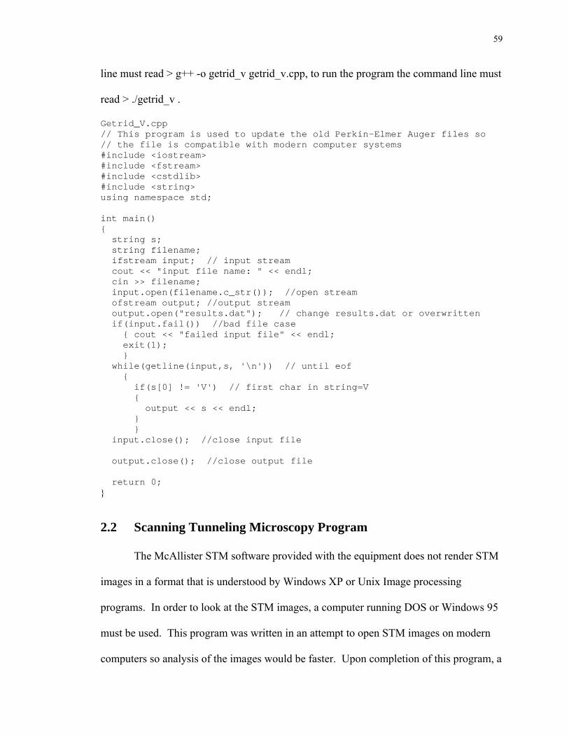
59
line must read > g++ -o getrid_v getrid_v.cpp, to run the program the command line must
read > ./getrid_v .
Getrid_V.cpp // This program is used to update the old Perkin-Elmer Auger files so // the file is compatible with modern computer systems #include <iostream> #include <fstream> #include <cstdlib> #include <string> using namespace std; int main() { string s; string filename; ifstream input; // input stream cout << "input file name: " << endl; cin >> filename; input.open(filename.c_str()); //open stream ofstream output; //output stream output.open("results.dat"); // change results.dat or overwritten if(input.fail()) //bad file case { cout << "failed input file" << endl; exit(1); } while(getline(input,s, '\n')) // until eof { if(s[0] != 'V') // first char in string=V { output << s << endl; } } input.close(); //close input file output.close(); //close output file return 0; }
2.2 Scanning Tunneling Microscopy Program
The McAllister STM software provided with the equipment does not render STM
images in a format that is understood by Windows XP or Unix Image processing
programs. In order to look at the STM images, a computer running DOS or Windows 95
must be used. This program was written in an attempt to open STM images on modern
computers so analysis of the images would be faster. Upon completion of this program, a
60
more versatile free software, “Scanning Probe Image Processor,” was discovered that
both converted the file format and provided many tools to make analysis easier.
// The purpose of this program is to update the old .STM file to a new // .PGM file for conversion and then use in a modern imaging software // program. #include <iostream> #include <fstream> #include <cstdlib> #include <string> using namespace std; int main() { string s; int length; char * buffer; string filename; ifstream input; // input stream input.open("04170609.STM"); //open stream ofstream output; //output stream output.open("convert.pgm"); // change results.dat or overwritten ofstream datput; datput.open("stm2int1.dat"); //binary to int data in row form if(input.fail()) //bad file case { cout << "failed input file" << endl; exit(1); } output<< "P5"<< " " << 400 << " " << 400 << endl; output << 255 << endl; //get length of file input.seekg (0, ios::end); length = input.tellg(); input.seekg (0,ios::beg); // allocate memory: buffer = new char [length]; int data_offset = 780; //read data as a block input.read( buffer,length); float max_max =0; for(int i=data_offset; i<length; i=i+2 ) { datput << (int) buffer[i] <<" " << (int) buffer[i+1] << endl; int number = abs(buffer[i]) + 128; int exponent = buffer[i+1]*255+number;
61
if ( exponent > max_max) { max_max = exponent; } // if((int) buffer[i]<0 ) cout << (int) buffer[i] << endl; //output << number; } char curr_Value; float scaled_Value; for(int i=data_offset; i<length; i=i+2 ) { float number = abs(buffer[i]) + 128; float exponent = buffer[i+1]*255+number; scaled_Value = (exponent/max_max)*255.0; curr_Value = scaled_Value; if(scaled_Value >255) cout << scaled_Value <<endl; output<< curr_Value; } input.close(); //close input file output.close(); //close output file datput.close(); return 0; }
Recommended