April 2007
FAN
7530 Critical C
onduction Mode PFC
Controller
© 2006 Fairchild Semiconductor Corporation www.fairchildsemi.comFAN7530 Rev. 1.0.2
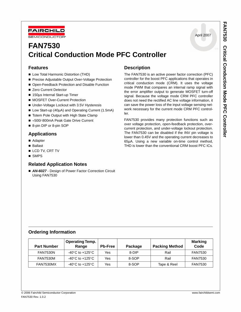
FAN7530Critical Conduction Mode PFC ControllerFeatures
Low Total Harmonic Distortion (THD)Precise Adjustable Output Over-Voltage ProtectionOpen-Feedback Protection and Disable FunctionZero Current Detector150µs Internal Start-up Timer MOSFET Over-Current ProtectionUnder-Voltage Lockout with 3.5V HysteresisLow Start-up (40µA) and Operating Current (1.5mA)Totem Pole Output with High State Clamp+500/-800mA Peak Gate Drive Current8-pin DIP or 8-pin SOP
ApplicationsAdapterBallastLCD TV, CRT TVSMPS
Related Application NotesAN-6027 - Design of Power Factor Correction Circuit Using FAN7530
Description The FAN7530 is an active power factor correction (PFC)controller for the boost PFC applications that operates incritical conduction mode (CRM). It uses the voltagemode PWM that compares an internal ramp signal withthe error amplifier output to generate MOSFET turn-offsignal. Because the voltage mode CRM PFC controllerdoes not need the rectified AC line voltage information, itcan save the power loss of the input voltage sensing net-work necessary for the current mode CRM PFC control-ler.
FAN7530 provides many protection functions such asover voltage protection, open-feedback protection, over-current protection, and under-voltage lockout protection.The FAN7530 can be disabled if the INV pin voltage islower than 0.45V and the operating current decreases to65µA. Using a new variable on-time control method,THD is lower than the conventional CRM boost PFC ICs.
Ordering Information
Part NumberOperating Temp.
Range Pb-Free Package Packing MethodMarking
CodeFAN7530N -40°C to +125°C Yes 8-DIP Rail FAN7530
FAN7530M -40°C to +125°C Yes 8-SOP Rail FAN7530
FAN7530MX -40°C to +125°C Yes 8-SOP Tape & Reel FAN7530
FAN
7530 Critical C
onduction Mode PFC
Controller
© 2006 Fairchild Semiconductor Corporation www.fairchildsemi.comFAN7530 Rev. 1.0.2 2
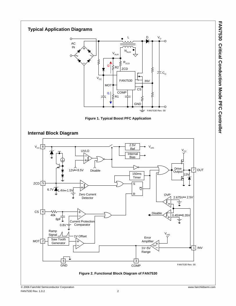
Typical Application Diagrams
Figure 1. Typical Boost PFC Application
Internal Block Diagram
Figure 2. Functional Block Diagram of FAN7530
GND
ZCD
INVVCC
ACIN
VO
COMP
FAN7530
CSMOT
R1
R2
L D
NAUXVAUX
RZCDI2
I1
CO
FAN7530 Rev. 00
INV
ErrorAmplifier
Vref1
OVP
COMP
8pF40k
2.5VRef
InternalBias
150msTimer
VCC
ZCD
CS
UVLO
6.7V
12V 8.5V
2.675V 2.5V
Current ProtectionComparator
1V OffsetMOT
GND
Saw ToothGenerator
Zero CurrentDetector
R
SQ
2
6
4
5
3
1
8 Vref1
Gm
0.8V
Disable
0.45V 0.35VDisable
1.5V1.4V
7
VCC
OUTDriveOutput
RampSignal
1V~5VRange
13V
FAN7530 Rev. 00
FAN
7530 Critical C
onduction Mode PFC
Controller
© 2006 Fairchild Semiconductor Corporation www.fairchildsemi.comFAN7530 Rev. 1.0.2 3
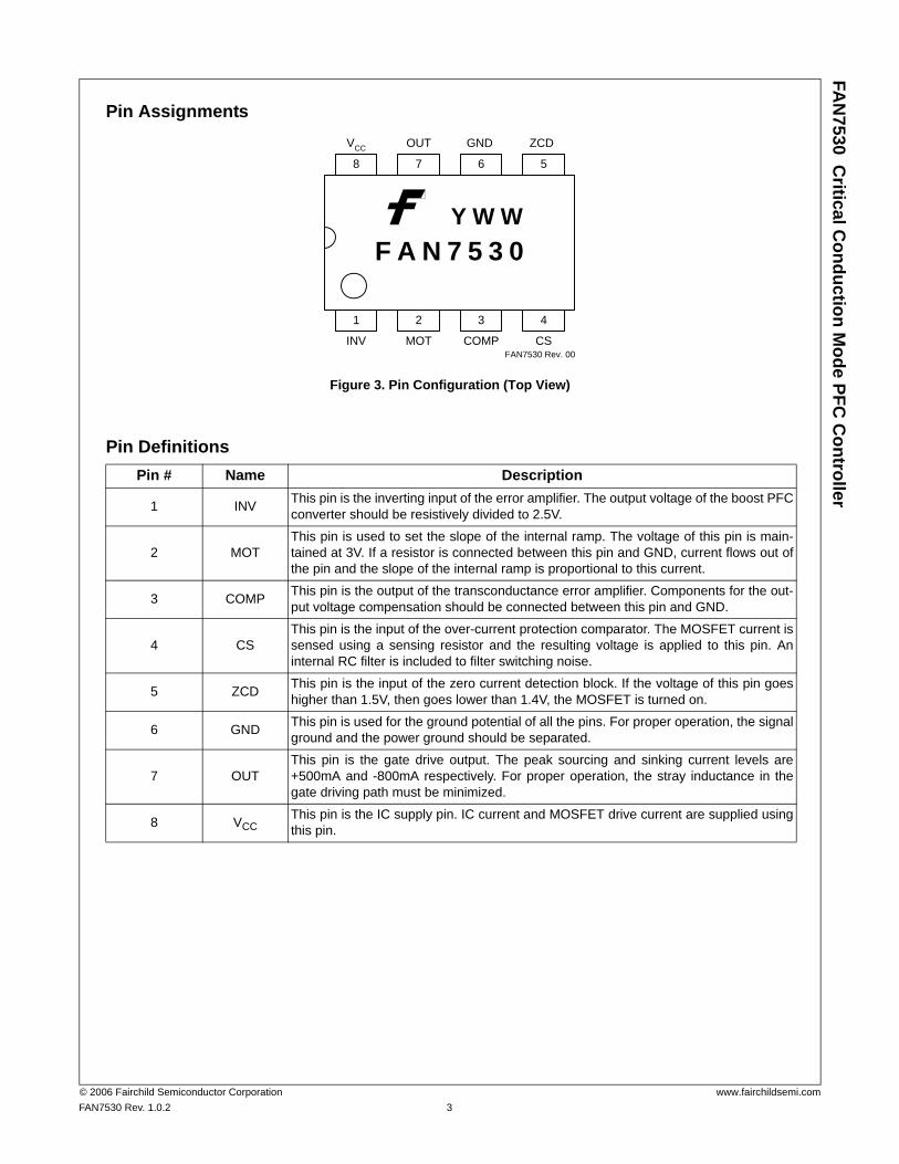
Pin Assignments
Figure 3. Pin Configuration (Top View)
Pin DefinitionsPin # Name Description
1 INV This pin is the inverting input of the error amplifier. The output voltage of the boost PFCconverter should be resistively divided to 2.5V.
2 MOTThis pin is used to set the slope of the internal ramp. The voltage of this pin is main-tained at 3V. If a resistor is connected between this pin and GND, current flows out ofthe pin and the slope of the internal ramp is proportional to this current.
3 COMP This pin is the output of the transconductance error amplifier. Components for the out-put voltage compensation should be connected between this pin and GND.
4 CSThis pin is the input of the over-current protection comparator. The MOSFET current issensed using a sensing resistor and the resulting voltage is applied to this pin. Aninternal RC filter is included to filter switching noise.
5 ZCD This pin is the input of the zero current detection block. If the voltage of this pin goeshigher than 1.5V, then goes lower than 1.4V, the MOSFET is turned on.
6 GND This pin is used for the ground potential of all the pins. For proper operation, the signalground and the power ground should be separated.
7 OUTThis pin is the gate drive output. The peak sourcing and sinking current levels are+500mA and -800mA respectively. For proper operation, the stray inductance in thegate driving path must be minimized.
8 VCCThis pin is the IC supply pin. IC current and MOSFET drive current are supplied usingthis pin.
F A N 7 5 3 0
6 58 7
VCC OUT GND ZCD
1 2 3 4
COMP CSMOTINV
Y W W
FAN7530 Rev. 00
FAN
7530 Critical C
onduction Mode PFC
Controller
© 2006 Fairchild Semiconductor Corporation www.fairchildsemi.comFAN7530 Rev. 1.0.2 4
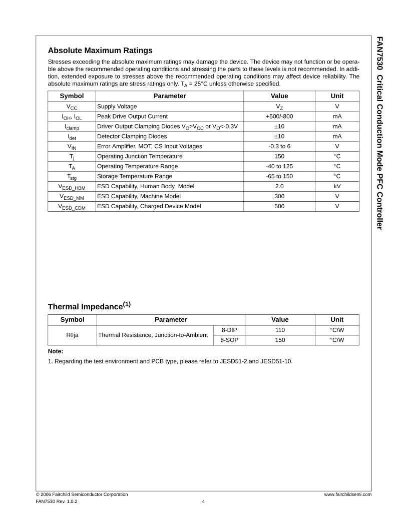
Absolute Maximum Ratings Stresses exceeding the absolute maximum ratings may damage the device. The device may not function or be opera-ble above the recommended operating conditions and stressing the parts to these levels is not recommended. In addi-tion, extended exposure to stresses above the recommended operating conditions may affect device reliability. Theabsolute maximum ratings are stress ratings only. TA = 25°C unless otherwise specified.
Thermal Impedance(1)
Note:1. Regarding the test environment and PCB type, please refer to JESD51-2 and JESD51-10.
Symbol Parameter Value UnitVCC Supply Voltage VZ V
IOH, IOL Peak Drive Output Current +500/-800 mA
Iclamp Driver Output Clamping Diodes VO>VCC or VO<-0.3V ±10 mA
Idet Detector Clamping Diodes ±10 mA
VIN Error Amplifier, MOT, CS Input Voltages -0.3 to 6 V
Tj Operating Junction Temperature 150 °C
TA Operating Temperature Range -40 to 125 °C
Tstg Storage Temperature Range -65 to 150 °C
VESD_HBM ESD Capability, Human Body Model 2.0 kV
VESD_MM ESD Capability, Machine Model 300 V
VESD_CDM ESD Capability, Charged Device Model 500 V
Symbol Parameter Value Unit
Rθja Thermal Resistance, Junction-to-Ambient8-DIP 110 °C/W
8-SOP 150 °C/W
FAN
7530 Critical C
onduction Mode PFC
Controller
© 2006 Fairchild Semiconductor Corporation www.fairchildsemi.comFAN7530 Rev. 1.0.2 5
Electrical CharacteristicsVCC = 14V, TA = -40°C~125°C, unless otherwise specified.
Note:2. These parameters, although guaranteed by design, are not tested in mass production.
Symbol Parameter Condition Min. Typ. Max. Unit UNDER-VOLTAGE LOCKOUT SECTION
Vth(start) Start Threshold Voltage VCC increasing 11 12 13 V
Vth(stop) Stop Threshold Voltage VCC decreasing 7.5 8.5 9.5 V
HY(uvlo) UVLO Hysteresis 3.0 3.5 4.0 V
VZ Zener Voltage ICC = 20mA 20 22 24 V
SUPPLY CURRENT SECTIONIst Start-up Supply Current VCC = Vth(start) - 0.2V 40 70 µA
ICC Operating Supply Current Output no switching 1.5 3.0 mA
Idcc Dynamic Operating Supply Current 50kHz, Cl=1nF 2.5 4.0 mA
ICC(dis) Operating Current at Disable Vinv = 0V 20 65 95 µA
ERROR AMPLIFIER SECTIONVref1 Voltage Feedback Input Threshold1 TA = 25°C 2.465 2.500 2.535 V
ΔVref1 Line Regulation VCC = 14V ~ 20V 0.1 10.0 mV
ΔVref2 Temperature Stability of Vref1(2) 20 mV
Ib(ea) Input Bias Current Vinv = 1V ~ 4V -0.5 0.5 µA
Isource Output Source Current Vinv = Vref1 - 0.1V -12 µA
Isink Output Sink Current Vinv = Vref1 + 0.1V 12 µA
Veao(H) Output Upper Clamp Voltage Vinv = Vref1 - 0.1V 5.4 6.0 6.6 V
Veao(Z) Zero Duty Cycle Output Voltage 0.9 1.0 1.1 V
gm Transconductance(2) 90 115 140 µmho
MAXIMUM ON-TIME SECTION Vmot Maximum On-time Voltage Rmot = 40.5kΩ 2.784 2.900 3.016 V
Ton(max) Maximum On-time Programming Rmot = 40.5kΩ, TA = 25°C 19 24 29 µs
CURRENT SENSE SECTION
VCS(limit)Current Sense Input ThresholdVoltage Limit 0.7 0.8 0.9 V
Ib(cs) Input Bias Current VCS = 0V ~ 1V -1.0 -0.1 1.0 µA
td(cs)Current Sense Delay to Output(2) dV/dt = 1V/100ns,
From 0V to 5V 350 500 ns
FAN
7530 Critical C
onduction Mode PFC
Controller
© 2006 Fairchild Semiconductor Corporation www.fairchildsemi.comFAN7530 Rev. 1.0.2 6
Electrical Characteristics (Continued)
VCC = 14V, TA = -40°C~125°C, unless otherwise specified.
Note:3. These parameters, although guaranteed by design, are not tested in mass production.
Symbol Parameter Condition Min. Typ. Max. Unit ZERO CURRENT DETECT SECTION
Vth(ZCD) Input Voltage Threshold(3) 1.35 1.50 1.65 V
HY(ZCD) Detect Hysteresis(3) 0.05 0.10 0.15 V
Vclamp(H) Input High Clamp Voltage Idet = 3mA 6.0 6.7 7.4 V
Vclamp(L) Input Low Clamp Voltage Idet = -3mA 0 0.65 1.00 V
Ib(ZCD) Input Bias Current VZCD = 1V ~ 5V -1.0 -0.1 1.0 µA
Isource(zcd) Source Current Capability(3) TA = 25°C -10 mA
Isink(zcd) Sink Current Capability(3) TA = 25°C 10 mA
tdeadMaximum Delay from ZCD to OutputTurn-on(3)
dV/dt = -1V/100ns,From 5V to 0V 100 200 ns
OUTPUT SECTION VOH Output Voltage High IO = -100mA, TA = 25°C 9.2 11.0 12.8 V
VOL Output Voltage Low IO = 200mA, TA = 25°C 1.0 2.5 V
tr Rising Time(3) Cl = 1nF 50 100 ns
tf Falling Time(3) Cl = 1nF 50 100 ns
VO(max) Maximum Output Voltage VCC = 20V, IO = 100μA 11.5 13.0 14.5 V
VO(UVLO) Output Voltage with UVLO Activated VCC = 5V, IO = 100μA 1 V
RESTART TIMER SECTIONtd(rst) Restart Timer Delay 50 150 300 µs
OVER-VOLTAGE PROTECTION SECTIONVovp OVP Threshold Voltage TA = 25°C 2.620 2.675 2.730 V
HY(ovp) OVP Hysteresis TA = 25°C 0.120 0.175 0.230 V
ENABLE SECTIONVth(en) Enable Threshold Voltage 0.40 0.45 0.50 V
HY(en) Enable Hysteresis 0.05 0.10 0.15 V
FAN
7530 Critical C
onduction Mode PFC
Controller
© 2006 Fairchild Semiconductor Corporation www.fairchildsemi.comFAN7530 Rev. 1.0.2 7
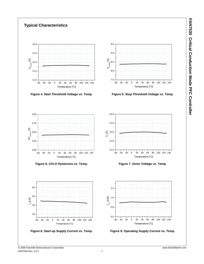
Typical Characteristics
Figure 4. Start Threshold Voltage vs. Temp. Figure 5. Stop Threshold Voltage vs. Temp.
Figure 6. UVLO Hysteresis vs. Temp. Figure 7. Zener Voltage vs. Temp.
Figure 8. Start-up Supply Current vs. Temp. Figure 9. Operating Supply Current vs. Temp.
-60 -40 -20 0 20 40 60 80 100 120 14011.0
11.5
12.0
12.5
13.0
Vth
(sta
rt) [V
]
Temperature [°C]
-60 -40 -20 0 20 40 60 80 100 120 1407.5
8.0
8.5
9.0
9.5
V th(s
top) [V
]
Temperature [°C]
-60 -40 -20 0 20 40 60 80 100 120 1403.00
3.25
3.50
3.75
4.00
HY
(UV
LO) [V
]
Temperature [°C]
-60 -40 -20 0 20 40 60 80 100 120 14021.0
21.5
22.0
22.5
23.0
V Z [V]
Temperature [°C]
-60 -40 -20 0 20 40 60 80 100 120 140
15
30
45
60
I st [μ
A]
Temperature [°C]
-60 -40 -20 0 20 40 60 80 100 120 1400.0
0.8
1.6
2.4
I CC [m
A]
Temperature [°C]
FAN
7530 Critical C
onduction Mode PFC
Controller
© 2006 Fairchild Semiconductor Corporation www.fairchildsemi.comFAN7530 Rev. 1.0.2 8
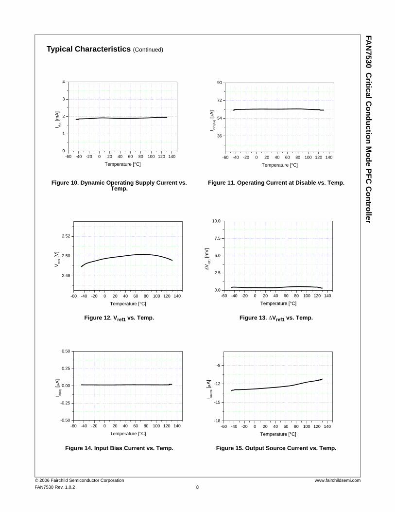
Typical Characteristics (Continued)
Figure 10. Dynamic Operating Supply Current vs. Temp.
Figure 11. Operating Current at Disable vs. Temp.
Figure 12. Vref1 vs. Temp. Figure 13. ΔVref1 vs. Temp.
Figure 14. Input Bias Current vs. Temp. Figure 15. Output Source Current vs. Temp.
-60 -40 -20 0 20 40 60 80 100 120 1400
1
2
3
4
I dcc [m
A]
Temperature [°C]-60 -40 -20 0 20 40 60 80 100 120 140
36
54
72
90
I CC
(dis
) [μA
]
Temperature [°C]
-60 -40 -20 0 20 40 60 80 100 120 140
2.48
2.50
2.52
Vre
f1 [V
]
Temperature [°C]
-60 -40 -20 0 20 40 60 80 100 120 1400.0
2.5
5.0
7.5
10.0
ΔV re
f1 [m
V]
Temperature [°C]
-60 -40 -20 0 20 40 60 80 100 120 140-0.50
-0.25
0.00
0.25
0.50
I b(ea
) [μA]
Temperature [°C]-60 -40 -20 0 20 40 60 80 100 120 140
-18
-15
-12
-9
I sour
ce [μ
A]
Temperature [°C]
FAN
7530 Critical C
onduction Mode PFC
Controller
© 2006 Fairchild Semiconductor Corporation www.fairchildsemi.comFAN7530 Rev. 1.0.2 9
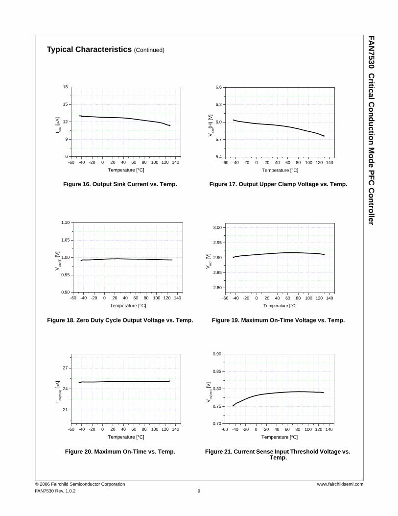
Typical Characteristics (Continued)
Figure 16. Output Sink Current vs. Temp. Figure 17. Output Upper Clamp Voltage vs. Temp.
Figure 18. Zero Duty Cycle Output Voltage vs. Temp. Figure 19. Maximum On-Time Voltage vs. Temp.
Figure 20. Maximum On-Time vs. Temp. Figure 21. Current Sense Input Threshold Voltage vs. Temp.
-60 -40 -20 0 20 40 60 80 100 120 1406
9
12
15
18
I sink
[μA
]
Temperature [°C]-60 -40 -20 0 20 40 60 80 100 120 140
5.4
5.7
6.0
6.3
6.6
V eao(H
) [V
]
Temperature [°C]
-60 -40 -20 0 20 40 60 80 100 120 1400.90
0.95
1.00
1.05
1.10
Vea
o(Z)
[V]
Temperature [°C]-60 -40 -20 0 20 40 60 80 100 120 140
2.80
2.85
2.90
2.95
3.00
Vm
ot [V
]
Temperature [°C]
-60 -40 -20 0 20 40 60 80 100 120 140
21
24
27
T on(m
ax) [μ
s]
Temperature [°C]-60 -40 -20 0 20 40 60 80 100 120 140
0.70
0.75
0.80
0.85
0.90
V cs(li
mit) [V
]
Temperature [°C]
FAN
7530 Critical C
onduction Mode PFC
Controller
© 2006 Fairchild Semiconductor Corporation www.fairchildsemi.comFAN7530 Rev. 1.0.2 10
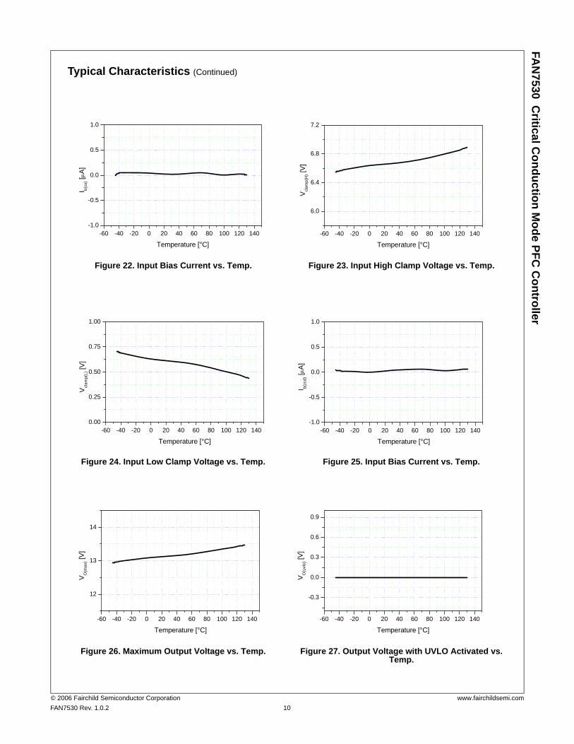
Typical Characteristics (Continued)
Figure 22. Input Bias Current vs. Temp. Figure 23. Input High Clamp Voltage vs. Temp.
Figure 24. Input Low Clamp Voltage vs. Temp. Figure 25. Input Bias Current vs. Temp.
Figure 26. Maximum Output Voltage vs. Temp. Figure 27. Output Voltage with UVLO Activated vs. Temp.
-60 -40 -20 0 20 40 60 80 100 120 140-1.0
-0.5
0.0
0.5
1.0
I b(cs
) [μA]
Temperature [°C]-60 -40 -20 0 20 40 60 80 100 120 140
6.0
6.4
6.8
7.2
V clam
p(H
) [V]
Temperature [°C]
-60 -40 -20 0 20 40 60 80 100 120 1400.00
0.25
0.50
0.75
1.00
Vcl
amp(
L) [V
]
Temperature [°C]-60 -40 -20 0 20 40 60 80 100 120 140
-1.0
-0.5
0.0
0.5
1.0
I b(zc
d) [μ
A]
Temperature [°C]
-60 -40 -20 0 20 40 60 80 100 120 140
12
13
14
VO
(max
) [V]
Temperature [°C]-60 -40 -20 0 20 40 60 80 100 120 140
-0.3
0.0
0.3
0.6
0.9
V O(u
vlo) [V
]
Temperature [°C]
FAN
7530 Critical C
onduction Mode PFC
Controller
© 2006 Fairchild Semiconductor Corporation www.fairchildsemi.comFAN7530 Rev. 1.0.2 11
Typical Characteristics (Continued)
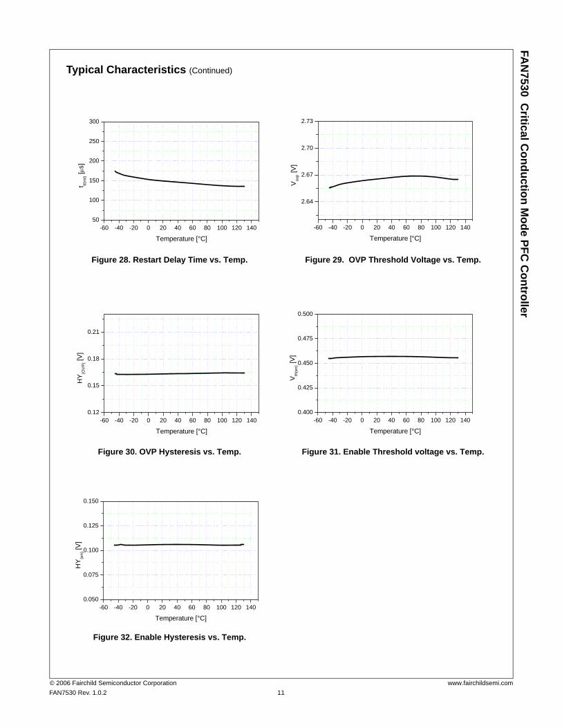
Figure 28. Restart Delay Time vs. Temp. Figure 29. OVP Threshold Voltage vs. Temp.
Figure 30. OVP Hysteresis vs. Temp. Figure 31. Enable Threshold voltage vs. Temp.
Figure 32. Enable Hysteresis vs. Temp.
-60 -40 -20 0 20 40 60 80 100 120 14050
100
150
200
250
300
t d(rs
t) [μs]
Temperature [°C]
-60 -40 -20 0 20 40 60 80 100 120 140
2.64
2.67
2.70
2.73
Vov
p [V]
Temperature [°C]
-60 -40 -20 0 20 40 60 80 100 120 1400.12
0.15
0.18
0.21
HY
(OV
P) [V
]
Temperature [°C]
-60 -40 -20 0 20 40 60 80 100 120 1400.400
0.425
0.450
0.475
0.500
V th(e
n) [V
]
Temperature [°C]
-60 -40 -20 0 20 40 60 80 100 120 1400.050
0.075
0.100
0.125
0.150
HY
(en) [V
]
Temperature [°C]
FAN
7530 Critical C
onduction Mode PFC
Controller
© 2006 Fairchild Semiconductor Corporation www.fairchildsemi.comFAN7530 Rev. 1.0.2 12
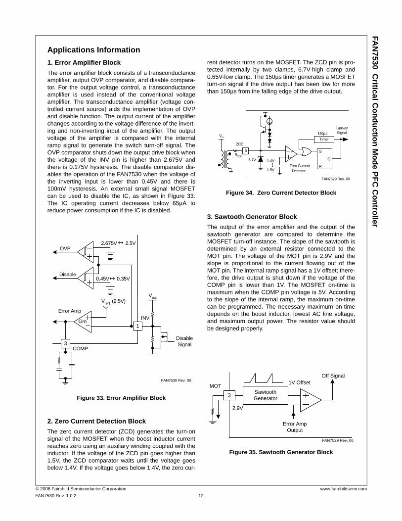
Applications Information 1. Error Amplifier BlockThe error amplifier block consists of a transconductanceamplifier, output OVP comparator, and disable compara-tor. For the output voltage control, a transconductanceamplifier is used instead of the conventional voltageamplifier. The transconductance amplifier (voltage con-trolled current source) aids the implementation of OVPand disable function. The output current of the amplifierchanges according to the voltage difference of the invert-ing and non-inverting input of the amplifier. The outputvoltage of the amplifier is compared with the internalramp signal to generate the switch turn-off signal. TheOVP comparator shuts down the output drive block whenthe voltage of the INV pin is higher than 2.675V andthere is 0.175V hysteresis. The disable comparator dis-ables the operation of the FAN7530 when the voltage ofthe inverting input is lower than 0.45V and there is100mV hysteresis. An external small signal MOSFETcan be used to disable the IC, as shown in Figure 33.The IC operating current decreases below 65µA toreduce power consumption if the IC is disabled.
Figure 33. Error Amplifier Block
2. Zero Current Detection BlockThe zero current detector (ZCD) generates the turn-onsignal of the MOSFET when the boost inductor currentreaches zero using an auxiliary winding coupled with theinductor. If the voltage of the ZCD pin goes higher than1.5V, the ZCD comparator waits until the voltage goesbelow 1.4V. If the voltage goes below 1.4V, the zero cur-
rent detector turns on the MOSFET. The ZCD pin is pro-tected internally by two clamps, 6.7V-high clamp and0.65V-low clamp. The 150µs timer generates a MOSFETturn-on signal if the drive output has been low for morethan 150µs from the falling edge of the drive output.
Figure 34. Zero Current Detector Block
3. Sawtooth Generator BlockThe output of the error amplifier and the output of thesawtooth generator are compared to determine theMOSFET turn-off instance. The slope of the sawtooth isdetermined by an external resistor connected to theMOT pin. The voltage of the MOT pin is 2.9V and theslope is proportional to the current flowing out of theMOT pin. The internal ramp signal has a 1V offset; there-fore, the drive output is shut down if the voltage of theCOMP pin is lower than 1V. The MOSFET on-time ismaximum when the COMP pin voltage is 5V. Accordingto the slope of the internal ramp, the maximum on-timecan be programmed. The necessary maximum on-timedepends on the boost inductor, lowest AC line voltage,and maximum output power. The resistor value shouldbe designed properly.
Figure 35. Sawtooth Generator Block
INVError Amp
OVP
COMP
2.675V 2.5V
3
1Gm
0.45V 0.35VDisable
VoutVref1 (2.5V)
DisableSignal
FAN7530 Rev. 00
TimerZCD
6.7VZero Current
DetectorR
S
Q
5
1.5V
1.4V
Vin
RZCD
150μsTurn-onSignal
FAN7529 Rev. 00
1V OffsetMOT
3
Error AmpOutput
Off Signal
2.9V
SawtoothGenerator
FAN7529 Rev. 00
FAN
7530 Critical C
onduction Mode PFC
Controller
© 2006 Fairchild Semiconductor Corporation www.fairchildsemi.comFAN7530 Rev. 1.0.2 13
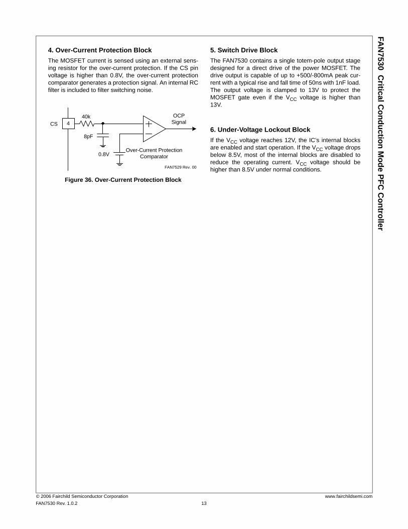
4. Over-Current Protection BlockThe MOSFET current is sensed using an external sens-ing resistor for the over-current protection. If the CS pinvoltage is higher than 0.8V, the over-current protectioncomparator generates a protection signal. An internal RCfilter is included to filter switching noise.
Figure 36. Over-Current Protection Block
5. Switch Drive BlockThe FAN7530 contains a single totem-pole output stagedesigned for a direct drive of the power MOSFET. Thedrive output is capable of up to +500/-800mA peak cur-rent with a typical rise and fall time of 50ns with 1nF load.The output voltage is clamped to 13V to protect theMOSFET gate even if the VCC voltage is higher than13V.
6. Under-Voltage Lockout BlockIf the VCC voltage reaches 12V, the IC’s internal blocksare enabled and start operation. If the VCC voltage dropsbelow 8.5V, most of the internal blocks are disabled toreduce the operating current. VCC voltage should behigher than 8.5V under normal conditions.
8pF
40kCS
Over-Current ProtectionComparator
4
0.8V
OCPSignal
FAN7529 Rev. 00
FAN
7530 Critical C
onduction Mode PFC
Controller
© 2006 Fairchild Semiconductor Corporation www.fairchildsemi.comFAN7530 Rev. 1.0.2 14
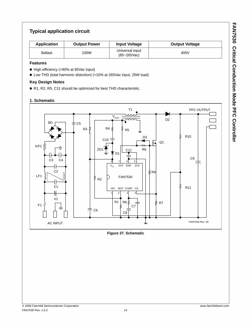
Typical application circuit
FeaturesHigh efficiency (>90% at 85Vac input)Low THD (total harmonic distortion) (<10% at 265Vac input, 25W load)
Key Design NotesR1, R2, R5, C11 should be optimized for best THD characteristic.
1. Schematic
Figure 37. Schematic
Application Output Power Input Voltage Output Voltage
Ballast 100W Universal input(85~265Vac) 400V
F1
AC INPUT
5678
OUTVCC GND ZCD
INV COMPMOT CS
FAN7530
1 2 3 4
V1
C1
C3 C4
LF1C2
NTC
BD C5
C6
R3 R4 R5
T1
D1
R7
R10
R6
D2
R9
Q1
VAUX
R2
R11
C9
ZD1
C10
PFC OUTPUT
D3
R1C7
R8
C8
C11
FAN7530 Rev. 00
FAN
7530 Critical C
onduction Mode PFC
Controller
© 2006 Fairchild Semiconductor Corporation www.fairchildsemi.comFAN7530 Rev. 1.0.2 15
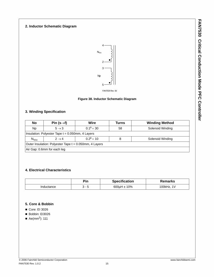
2. Inductor Schematic Diagram
Figure 38. Inductor Schematic Diagram
3. Winding Specification
4. Electrical Characteristics
5. Core & BobbinCore: EI 3026Bobbin: EI3026Ae(mm2): 111
No Pin (s→f) Wire Turns Winding MethodNp 5 → 3 0.1φ × 30 58 Solenoid Winding
Insulation: Polyester Tape t = 0.050mm, 4 Layers
NVcc 2 → 4 0.2φ × 10 8 Solenoid Winding
Outer Insulation: Polyester Tape t = 0.050mm, 4 Layers
Air Gap: 0.6mm for each leg
Pin Specification RemarksInductance 3 - 5 600µH ± 10% 100kHz, 1V
Np
4
2
NVcc
5
3
FAN7529 Rev. 00
FAN
7530 Critical C
onduction Mode PFC
Controller
© 2006 Fairchild Semiconductor Corporation www.fairchildsemi.comFAN7530 Rev. 1.0.2 16
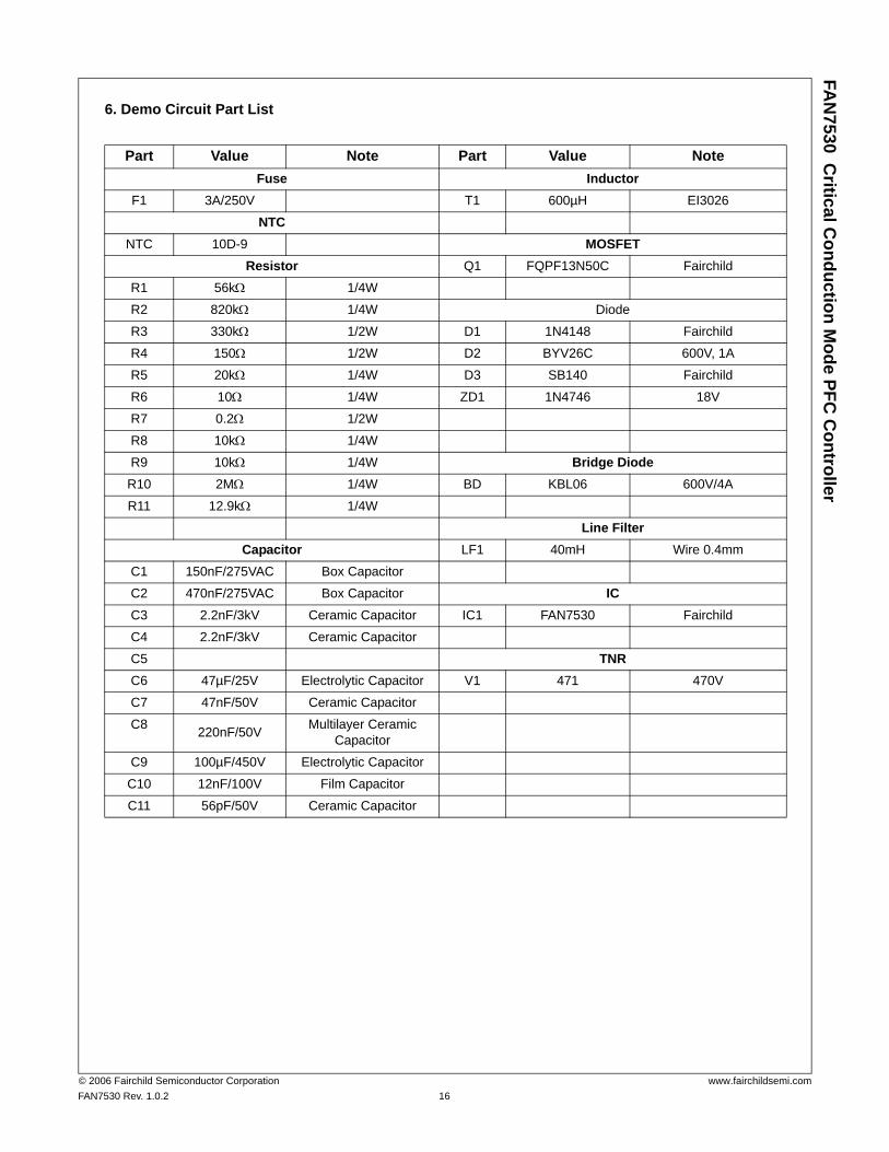
6. Demo Circuit Part List
Part Value Note Part Value NoteFuse Inductor
F1 3A/250V T1 600µH EI3026
NTCNTC 10D-9 MOSFET
Resistor Q1 FQPF13N50C Fairchild
R1 56kΩ 1/4W
R2 820kΩ 1/4W Diode
R3 330kΩ 1/2W D1 1N4148 Fairchild
R4 150Ω 1/2W D2 BYV26C 600V, 1A
R5 20kΩ 1/4W D3 SB140 Fairchild
R6 10Ω 1/4W ZD1 1N4746 18V
R7 0.2Ω 1/2W
R8 10kΩ 1/4W
R9 10kΩ 1/4W Bridge DiodeR10 2MΩ 1/4W BD KBL06 600V/4A
R11 12.9kΩ 1/4W
Line FilterCapacitor LF1 40mH Wire 0.4mm
C1 150nF/275VAC Box Capacitor
C2 470nF/275VAC Box Capacitor ICC3 2.2nF/3kV Ceramic Capacitor IC1 FAN7530 Fairchild
C4 2.2nF/3kV Ceramic Capacitor
C5 TNRC6 47µF/25V Electrolytic Capacitor V1 471 470V
C7 47nF/50V Ceramic Capacitor
C8 220nF/50V Multilayer Ceramic Capacitor
C9 100µF/450V Electrolytic Capacitor
C10 12nF/100V Film Capacitor
C11 56pF/50V Ceramic Capacitor
FAN
7530 Critical C
onduction Mode PFC
Controller
© 2006 Fairchild Semiconductor Corporation www.fairchildsemi.comFAN7530 Rev. 1.0.2 17
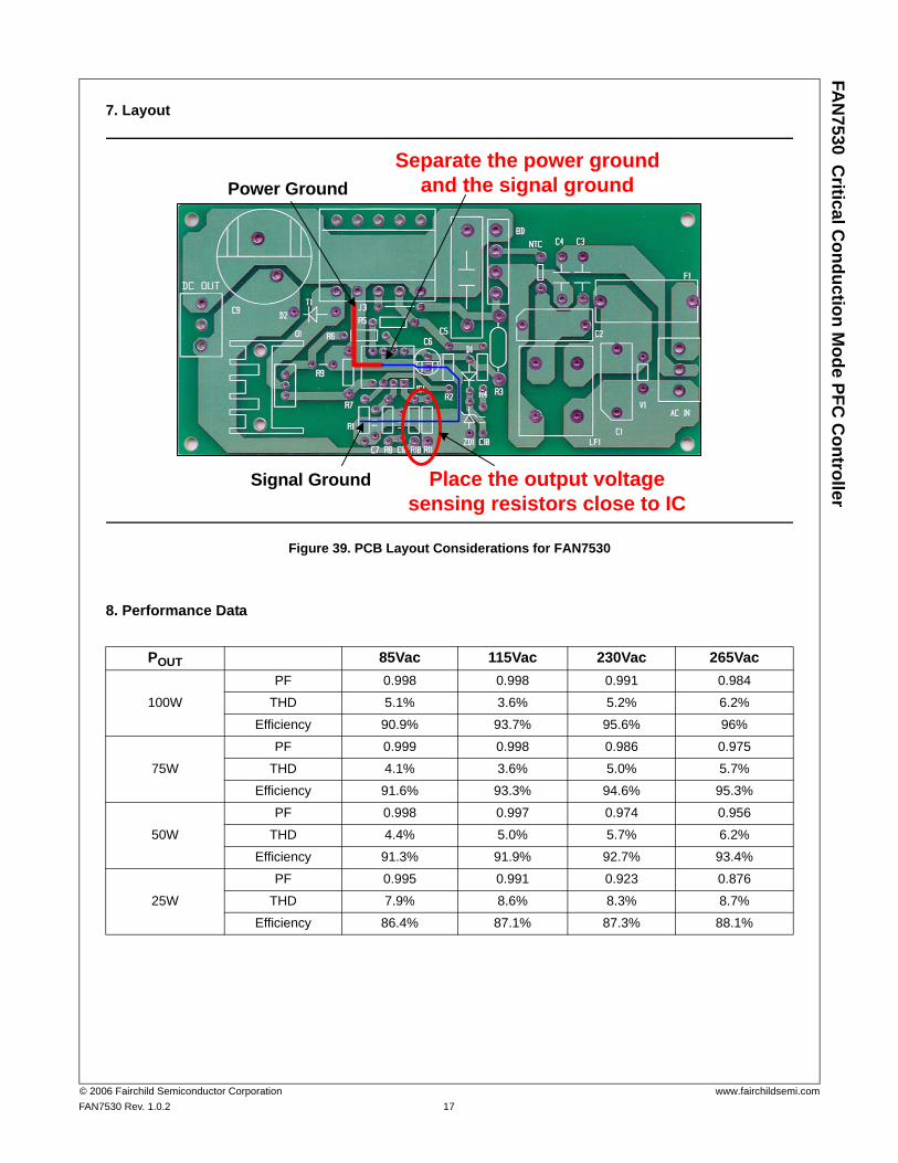
7. Layout
Figure 39. PCB Layout Considerations for FAN7530
8. Performance Data
POUT 85Vac 115Vac 230Vac 265Vac
100W
PF 0.998 0.998 0.991 0.984
THD 5.1% 3.6% 5.2% 6.2%
Efficiency 90.9% 93.7% 95.6% 96%
75W
PF 0.999 0.998 0.986 0.975
THD 4.1% 3.6% 5.0% 5.7%
Efficiency 91.6% 93.3% 94.6% 95.3%
50W
PF 0.998 0.997 0.974 0.956
THD 4.4% 5.0% 5.7% 6.2%
Efficiency 91.3% 91.9% 92.7% 93.4%
25W
PF 0.995 0.991 0.923 0.876
THD 7.9% 8.6% 8.3% 8.7%
Efficiency 86.4% 87.1% 87.3% 88.1%
Power Ground
Signal Ground
Separate the power groundand the signal ground
Place the output voltagesensing resistors close to IC
FAN
7530 Critical C
onduction Mode PFC
Controller
© 2006 Fairchild Semiconductor Corporation www.fairchildsemi.comFAN7530 Rev. 1.0.2 18
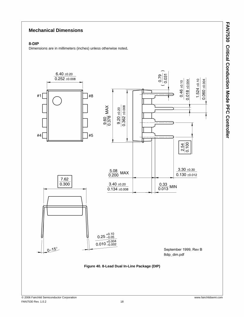
Mechanical Dimensions
8-DIPDimensions are in millimeters (inches) unless otherwise noted..
Figure 40. 8-Lead Dual In-Line Package (DIP)
September 1999, Rev B
6.40 ±0.20
3.30 ±0.30
0.130 ±0.012
3.40 ±0.20
0.134 ±0.008
#1
#4 #5
#8
0.252 ±0.008
9.20
±0.2
0
0.79
2.54
0.10
0
0.03
1(
)
0.46
±0.1
0
0.01
8±0
.004
0.06
0±0
.004
1.52
4±0
.10
0.36
2±0
.008
9.60
0.37
8M
AX
5.080.200
0.330.013
7.62
0~15°
0.300
MAX
MIN
0.25+0.10–0.05
0.010+0.004–0.002
8dip_dim.pdf
FAN
7530 Critical C
onduction Mode PFC
Controller
© 2006 Fairchild Semiconductor Corporation www.fairchildsemi.comFAN7530 Rev. 1.0.2 19
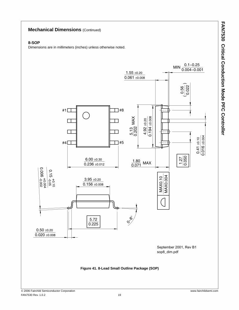
Mechanical Dimensions (Continued)
8-SOPDimensions are in millimeters (inches) unless otherwise noted.
Figure 41. 8-Lead Small Outline Package (SOP)
September 2001, Rev B1sop8_dim.pdf
4.92
±0.2
0
0.19
4±0
.008
0.41
±0.1
0
0.01
6±0
.004
1.27
0.05
0
5.720.225
1.55 ±0.20
0.061 ±0.008
0.1~0.250.004~0.001
6.00 ±0.30
0.236 ±0.012
3.95 ±0.20
0.156 ±0.008
0.50 ±0.20
0.020 ±0.008
5.13
0.20
2M
AX
#1
#4 #5
0~8°
#8
0.56
0.02
2(
)
1.800.071
MA
X0.
10M
AX
0.00
4MAX
MIN
+0.10
-0.050.15
+0.004
-0.0020.006
TRADEMARKS
The following are registered and unregistered trademarks Fairchild Semiconductor owns or is authorized to use and is not intended to be an exhaustive list of all such trademarks.
ACEx®
Across the board. Around the world.ActiveArrayBottomlessBuild it NowCoolFETCROSSVOLTCTL™Current Transfer Logic™ DOMEE2CMOSEcoSPARK®
EnSignaFACT Quiet Series™ FACT®
FAST®
FASTrFPSFRFET®
GlobalOptoisolatorGTOHiSeC
i-LoImpliedDisconnectIntelliMAXISOPLANARMICROCOUPLERMicroPakMICROWIREMotion-SPM™MSXMSXProOCXOCXProOPTOLOGIC®
OPTOPLANAR®
PACMANPDP-SPM™POPPower220®
Power247®
PowerEdgePowerSaver
Power-SPMPowerTrench®
Programmable Active DroopQFET®
QSQT OptoelectronicsQuiet SeriesRapidConfigureRapidConnectScalarPumpSMART STARTSPM®
STEALTH™SuperFETSuperSOT -3SuperSOT -6SuperSOT -8SyncFET™ TCMThe Power Franchise®
™
TinyBoostTinyBuckTinyLogic®
TINYOPTOTinyPowerTinyWireTruTranslation
SerDesUHC®
UniFETVCXWire
DISCLAIMER
FAIRCHILD SEMICONDUCTOR RESERVES THE RIGHT TO MAKE CHANGES WITHOUT FURTHER NOTICE TO ANY PRODUCTS HEREIN TO IMPROVE RELIABILITY, FUNCTION OR DESIGN. FAIRCHILD DOES NOT ASSUME ANY LIABILITY ARISING OUT OF THE APPLICATION OR USE OF ANY PRODUCT OR CIRCUIT DESCRIBED HEREIN; NEITHER DOES IT CONVEY ANY LICENSE UNDER ITS PATENT RIGHTS, NOR THE RIGHTS OF OTHERS. THESE SPECIFICATIONS DO NOT EXPAND THE TERMS OF FAIRCHILD’S WORLDWIDE TERMS AND CONDITIONS, SPECIFICALLY THE WARRANTY THEREIN, WHICH COVERS THESE PRODUCTS.
LIFE SUPPORT POLICY
FAIRCHILD’S PRODUCTS ARE NOT AUTHORIZED FOR USE AS CRITICAL COMPONENTS IN LIFE SUPPORT DEVICES OR SYSTEMS WITHOUT THE EXPRESS WRITTEN APPROVAL OF FAIRCHILD SEMICONDUCTOR CORPORATION.
As used herein: 1. Life support devices or systems are devices or systems
which, (a) are intended for surgical implant into the body or (b) support or sustain life, and (c) whose failure to perform when properly used in accordance with instructions for use provided in the labeling, can be reasonably expected to result in a significant injury of the user.
2. A critical component in any component of a life support, device, or system whose failure to perform can be reasonably expected to cause the failure of the life support device or system, or to affect its safety or effectiveness.
PRODUCT STATUS DEFINITIONS
Definition of Terms
Datasheet Identification Product Status Definition
Advance Information Formative or In Design This datasheet contains the design specifications for product development. Specifications may change in any manner without notice.
Preliminary First Production This datasheet contains preliminary data; supplementary data will be published at a later date. Fairchild Semiconductor reserves the right to make changes at any time without notice to improve design.
No Identification Needed Full Production This datasheet contains final specifications. Fairchild Semiconductor reserves the right to make changes at any time without notice to improve design.
Obsolete Not In Production This datasheet contains specifications on a product that has been discontinued by Fairchild Semiconductor. The datasheet is printed for reference information only.
Rev. I26
FAN
7530 Critical C
onduction Mode PFC
Controller
© 2006 Fairchild Semiconductor Corporation www.fairchildsemi.comFAN7530 Rev. 1.0.2 20
Recommended