Computer Architecture, Memory System DesignFeb. 2011 Slide 1
Part VMemory System Design

Computer Architecture, Memory System DesignFeb. 2011 Slide 2
About This Presentation
This presentation is intended to support the use of the textbook Computer Architecture: From Microprocessors to Supercomputers, Oxford University Press, 2005, ISBN 0-19-515455-X. It is updated regularly by the author as part of his teaching of the upper-division course ECE 154, Introduction to Computer Architecture, at the University of California, Santa Barbara. Instructors can use these slides freely in classroom teaching and for other educational purposes. Any other use is strictly prohibited. ©
Behrooz Parhami
Edition Released Revised Revised Revised Revised
First July 2003 July 2004 July 2005 Mar. 2006 Mar. 2007
Mar. 2008 Feb. 2009 Feb. 2011

Computer Architecture, Memory System DesignFeb. 2011 Slide 3
V Memory System Design
Topics in This Part
Chapter 17 Main Memory Concepts
Chapter 18 Cache Memory Organization
Chapter 19 Mass Memory Concepts
Chapter 20 Virtual Memory and Paging
Design problem – We want a memory unit that:• Can keep up with the CPU’s processing speed• Has enough capacity for programs and data• Is inexpensive, reliable, and energy-efficient

Computer Architecture, Memory System DesignFeb. 2011 Slide 4
17 Main Memory Concepts Technologies & organizations for computer’s main memory
• SRAM (cache), DRAM (main), and flash (nonvolatile)• Interleaving & pipelining to get around “memory wall”
Topics in This Chapter
17.1 Memory Structure and SRAM
17.2 DRAM and Refresh Cycles
17.3 Hitting the Memory Wall
17.4 Interleaved and Pipelined Memory
17.5 Nonvolatile Memory
17.6 The Need for a Memory Hierarchy

Computer Architecture, Memory System DesignFeb. 2011 Slide 5
17.1 Memory Structure and SRAM
Fig. 17.1 Conceptual inner structure of a 2h g SRAM chip and its shorthand representation.
/ h
Write enable / g
Data in
Address
Data out
Chip select
Q
C
Q
D
FF
Q
C
Q
D
FF
Q
C
Q
D
FF
/
g
Output enable
1
0
2 –1 h
Address decoder
Storage cells
/
g
/
g
/
g
WE
CS
OE
D in D out
Addr
.
.
.

Computer Architecture, Memory System DesignFeb. 2011 Slide 6
Multiple-Chip SRAM
Fig. 17.2 Eight 128K 8 SRAM chips forming a 256K 32 memory unit.
/
WE
CS
OE
D in D out
Addr
WE
CS
OE
D in D out
Addr
WE
CS
OE
D in D out
Addr
WE
CS
OE
D in D out
Addr
WE
CS
OE
D in D out
Addr
WE
CS
OE
D in D out
Addr
WE
CS
OE
D in D out
Addr
18
/
17
32 WE
CS
OE
D in D out
Addr
Data in
Data out, byte 3
Data out, byte 2
Data out, byte 1
Data out, byte 0
MSB
Address

Jan. 2011 Computer Architecture, Background and Motivation Slide 7
SRAM
Figure 2.10 SRAM memory is simply a large, single-port register file.
Column mux
Row
dec
ode
r
/ h
Address
Square or almost square memory matrix
Row buffer
Row
Column
g bits data out
/
g /
h
Write enable
/
g
Data in
Address
Data out
Output enable
Chip select
.
.
.
. . .
. . .
(a) SRAM block diagram (b) SRAM read mechanism

Computer Architecture, Memory System DesignFeb. 2011 Slide 8
17.2 DRAM and Refresh Cycles
DRAM vs. SRAM Memory Cell Complexity
Word line
Capacitor
Bit line
Pass transistor
Word line
Bit line
Compl. bit line
Vcc
(a) DRAM cell (b) Typical SRAM cell
Fig. 17.4 Single-transistor DRAM cell, which is considerably simpler than SRAM cell, leads to dense, high-capacity DRAM memory chips.

Computer Architecture, Memory System DesignFeb. 2011 Slide 9
Fig. 17.5 Variations in the voltage across a DRAM cell capacitor after writing a 1 and subsequent refresh operations.
DRAM Refresh Cycles and Refresh Rate
Time
Threshold voltage
0 Stored
1 Written Refreshed Refreshed Refreshed
10s of ms before needing refresh cycle
Voltage for 1
Voltage for 0

Computer Architecture, Memory System DesignFeb. 2011 Slide 10
Loss of Bandwidth to Refresh Cycles
Example 17.2
A 256 Mb DRAM chip is organized as a 32M 8 memory externally and as a 16K 16K array internally. Rows must be refreshed at least once every 50 ms to forestall data loss; refreshing a row takes 100 ns. What fraction of the total memory bandwidth is lost to refresh cycles?
Solution
Refreshing all 16K rows takes 16 1024 100 ns = 1.64 ms. Loss of 1.64 ms every 50 ms amounts to 1.64/50 = 3.3% of the total bandwidth.

Computer Architecture, Memory System DesignFeb. 2011 Slide 11
DRAM Organization
Fig. 18.8 A 256 Mb DRAM chip organized as a 32M 8 memory.
16Kb 16Kb memory matrix
Selected row
Column mux
Row address decoder
16 Kb = 2 KB 14 / 11
/
Byte address
in
Data byte out
. . .
. . .
. . .

Computer Architecture, Memory System DesignFeb. 2011 Slide 12
DRAM Packaging
Fig. 17.6 Typical DRAM package housing a 4M 4 memory.
Legend:
Ai CAS Dj NC OE RAS WE
1 2 3 4 5 6 7 8 9 10 11 12
24 23 22 21 20 19 18 17 16 15 14 13
A4 A5 A6 A7 A8 A9 D3 D4 CAS OE Vss Vss
A0 A1 A2 A3 A10 D1 D2 RAS WE Vcc Vcc NC
Address bit i Column address strobe Data bit j No connection Output enable Row address strobe Write enable
24-pin dual in-line package (DIP)

Computer Architecture, Memory System DesignFeb. 2011 Slide 13
17.3 Hitting the Memory Wall
Fig. 17.8 Memory density and capacity have grown along with the CPU power and complexity, but memory speed has not kept pace.
1990 1980 2000 2010 1
10
10
Re
lati
ve p
erf
orm
anc
e
Calendar year
Processor
Memory
3
6

Computer Architecture, Memory System DesignFeb. 2011 Slide 14
17.4 Pipelined and Interleaved Memory
Address translation
Row decoding & read out
Column decoding
& selection
Tag comparison & validation
Fig. 17.10 Pipelined cache memory.
Memory latency may involve other supporting operationsbesides the physical access itself
Virtual-to-physical address translation (Chap 20) Tag comparison to determine cache hit/miss (Chap 18)

Computer Architecture, Memory System DesignFeb. 2011 Slide 15
Memory Interleaving
Fig. 17.11 Interleaved memory is more flexible than wide-access
memory in that it can handle multiple independent accesses at once.
Add- ress
Addresses that are 0 mod 4
Addresses that are 2 mod 4
Addresses that are 1 mod 4
Addresses that are 3 mod 4
Return data
Data in
Data out Dispatch
(based on 2 LSBs of address)
Bus cycle
Memory cycle
0
1
2
3
0
1
2
3
Module accessed
Time
Addresses 0, 4, 8, …
Addresses 1, 5, 9, …
Addresses 2, 6, 10, …
Addresses 3, 7, 11, …

Computer Architecture, Memory System DesignFeb. 2011 Slide 16
17.5 Nonvolatile Memory
Fig. 17.13 Flash memory organization.
S o u r c e l i n e s
B i t l i n e s
Word lines
n+
n
p subs- trate
Control gate
Floating gate
Source
Drain

Computer Architecture, Memory System DesignFeb. 2011 Slide 17
17.6 The Need for a Memory Hierarchy
The widening speed gap between CPU and main memory
Processor operations take of the order of 1 ns
Memory access requires 10s or even 100s of ns
Memory bandwidth limits the instruction execution rate
Each instruction executed involves at least one memory access
Hence, a few to 100s of MIPS is the best that can be achieved
A fast buffer memory can help bridge the CPU-memory gap
The fastest memories are expensive and thus not very large
A second intermediate cache level is thus often used

Computer Architecture, Memory System DesignFeb. 2011 Slide 18
Typical Levels in a Hierarchical Memory
Fig. 17.14 Names and key characteristics of levels in a memory hierarchy.
Tertiary Secondary
Main
Cache 2
Cache 1
Reg’s $Millions $100s Ks
$10s Ks
$1000s
$10s
$1s
Cost per GB Access latency Capacity
TBs 10s GB
100s MB
MBs
10s KB
100s B
min+ 10s ms
100s ns
10s ns
a few ns
ns
Speed gap

Computer Architecture, Memory System DesignFeb. 2011 Slide 19
18 Cache Memory Organization Processor speed is improving at a faster rate than memory’s
• Processor-memory speed gap has been widening• Cache is to main as desk drawer is to file cabinet
Topics in This Chapter
18.1 The Need for a Cache
18.2 What Makes a Cache Work?
18.3 Direct-Mapped Cache
18.4 Set-Associative Cache

Computer Architecture, Memory System DesignFeb. 2011 Slide 20
18.1 The Need for a Cache
/
ALU
Data cache
Instr cache
Next addr
Reg file
op
jta
fn
inst
imm
rs (rs)
(rt)
Data addr
Data in 0
1
ALUSrc ALUFunc DataWrite
DataRead
SE
RegInSrc
rt
rd
RegDst RegWrite
32 / 16
Register input
Data out
Func
ALUOvfl
Ovfl
31
0 1 2
Next PC
Incr PC
(PC)
Br&Jump
ALU out
PC
0 1 2
Single-cycle
/
16
rs
0 1
0 1 2
ALU
Cache Reg file
op
jta
fn
(rs)
(rt)
Address
Data
Inst Reg
Data Reg
x Reg
y Reg
z Reg PC
4
ALUSrcX
ALUFunc
MemWrite MemRead
RegInSrc
4
rd
RegDst
RegWrite
/
32
Func
ALUOvfl
Ovfl
31
PCSrc PCWrite
IRWrite
ALU out
0 1
0 1
0 1 2 3
0 1 2 3
InstData ALUSrcY
SysCallAddr
/
26
4
rt
ALUZero
Zero
x Mux
y Mux
0 1
JumpAddr
4 MSBs
/
30
30
SE
imm
Multicycle
ALU
Data cache
Instr cache
Next addr
Reg file
op fn
inst
imm
rs (rs)
(rt)
Data addr
ALUSrc ALUFunc
DataWrite DataRead
RegInSrc
rt
rd
RegDst RegWrite
Func
ALUOvfl
Ovfl
IncrPC
Br&Jump
PC
1 Incr
0
1
rt
31
0 1 2
NextPC
0
1
SeqInst
0 1 2
0 1
RetAddr
Stage 1 Stage 2 Stage 3 Stage 4 Stage 5
SE
5 3
2
Pipelined
125 MHzCPI = 1
500 MHzCPI 4
500 MHzCPI 1.1
All three of our MicroMIPS designs assumed 2-ns data and instruction memories; however, typical RAMs are 10-50 times slower

Computer Architecture, Memory System DesignFeb. 2011 Slide 21
Desktop, Drawer, and File Cabinet Analogy
Fig. 18.3 Items on a desktop (register) or in a drawer (cache) are more readily accessible than those in a file cabinet (main memory).
Main memory
Register file
Access cabinet in 30 s
Access desktop in 2 s
Access drawer in 5 s
Cache memory
Once the “working set” is in the drawer, very few trips to the file cabinet are needed.

Computer Architecture, Memory System DesignFeb. 2011 Slide 22
Cache, Hit/Miss Rate, and Effective Access Time
One level of cache with hit rate h
Ceff = hCfast + (1 – h)(Cslow + Cfast) = Cfast + (1 – h)Cslow
CPUCache(fast)
memory
Main(slow)
memory
Reg file
Word
Line
Data is in the cache fraction h of the time(say, hit rate of 98%)
Go to main 1 – h of the time(say, cache miss rate of 2%)
Cache is transparent to user;transfers occur automatically

Computer Architecture, Memory System DesignFeb. 2011 Slide 23
Multiple Cache Levels
Fig. 18.1 Cache memories act as intermediaries between the superfast processor and the much slower main memory.
Level-2 cache
Main memory
CPU CPU registers
Level-1 cache
Level-2 cache
Main memory
CPU CPU registers
Level-1 cache
(a) Level 2 between level 1 and main (b) Level 2 connected to “backside” bus
Cleaner and easier to analyze

Computer Architecture, Memory System DesignFeb. 2011 Slide 24
Performance of a Two-Level Cache System
Example 18.1
A system with L1 and L2 caches has a CPI of 1.2 with no cache miss. There are 1.1 memory accesses on average per instruction. What is the effective CPI with cache misses factored in?
Level Local hit rate Miss penalty L1 95 % 8 cycles L2 80 % 60 cycles
Level-2 cache
Main memory
CPU CPU registers
Level-1 cache
Level-2 cache
Main memory
CPU CPU registers
Level-1 cache
(a) Level 2 between level 1 and main (b) Level 2 connected to “backside” bus
8 cycles
60 cycles
95%4%
1%
Solution
Ceff = Cfast + (1 – h1)[Cmedium + (1 – h2)Cslow]
Because Cfast is included in the CPI of 1.2, we must account for the rest
CPI = 1.2 + 1.1(1 – 0.95)[8 + (1 – 0.8)60] = 1.2 + 1.1 0.05 20 = 2.3

Computer Architecture, Memory System DesignFeb. 2011 Slide 25
18.2 What Makes a Cache Work?
Fig. 18.2 Assuming no conflict in address mapping, the cache will hold a small program loop in its entirety, leading to fast execution.
9-instruction program loop
Address mapping (many-to-one)
Cache memory
Main memory
Cache l ine/block (unit of t ransfer between main and cache memories)
Temporal localitySpatial locality

Computer Architecture, Memory System DesignFeb. 2011 Slide 26
18.3 Direct-Mapped Cache
Fig. 18.4 Direct-mapped cache holding 32 words within eight 4-word lines. Each line is associated with a tag and a valid bit.
3-bit line index in cache
2-bit word offset in line Main memory locations
0-3 4-7
8-11
36-39 32-35
40-43
68-71 64-67 72-75
100-103 96-99 104-107
Tag Word
address
Valid bits
Tags
Read tag and specified word
Com-pare
1,Tag
Data out
Cache miss
1 if equal

Computer Architecture, Memory System DesignFeb. 2011 Slide 27
3-bit line index in cache
2-bit word offset in line Main memory locations
0-3 4-7
8-11
36-39 32-35
40-43
68-71 64-67 72-75
100-103 96-99 104-107
Tag Word
address
Valid bits
Tags
Read tag and specified word
Com-pare
1,Tag
Data out
Cache miss
1 if equal
Direct-Mapped Cache Behavior
Fig. 18.4
Address trace:1, 7, 6, 5, 32, 33, 1, 2, . . .
1: miss, line 3, 2, 1, 0 fetched 7: miss, line 7, 6, 5, 4 fetched 6: hit 5: hit32: miss, line 35, 34, 33, 32 fetched (replaces 3, 2, 1, 0)33: hit 1: miss, line 3, 2, 1, 0 fetched (replaces 35, 34, 33, 32) 2: hit ... and so on
1 0 3 2 5 4 7 633 3235 34 1 0 3 2

Computer Architecture, Memory System DesignFeb. 2011 Slide 28
18.4 Set-Associative Cache
Fig. 18.6 Two-way set-associative cache holding 32 words of data within 4-word lines and 2-line sets.
Main memory locations
0-3
16-19
32-35
48-51
64-67
80-83
96-99
112-115
Valid bits
Tags
1
0
2-bit set index in cache
2-bit word offset in line
Tag
Word address
Option 0
Option 1
Read tag and specified word from each option
Com-pare
1,Tag
Com-pare
Data out
Cache
miss
1 if equal

Computer Architecture, Memory System DesignFeb. 2011 Slide 29
Cache Memory Design Parameters
Cache size (in bytes or words). A larger cache can hold more of the program’s useful data but is more costly and likely to be slower.
Block or cache-line size (unit of data transfer between cache and main). With a larger cache line, more data is brought in cache with each miss. This can improve the hit rate but also may bring low-utility data in.
Placement policy. Determining where an incoming cache line is stored. More flexible policies imply higher hardware cost and may or may not have performance benefits (due to more complex data location).
Replacement policy. Determining which of several existing cache blocks (into which a new cache line can be mapped) should be overwritten. Typical policies: choosing a random or the least recently used block.
Write policy. Determining if updates to cache words are immediately forwarded to main (write-through) or modified blocks are copied back to main if and when they must be replaced (write-back or copy-back).

Computer Architecture, Memory System DesignFeb. 2011 Slide 30
19 Mass Memory Concepts
Today’s main memory is huge, but still inadequate for all needs• Magnetic disks provide extended and back-up storage• Optical disks & disk arrays are other mass storage options
Topics in This Chapter
19.1 Disk Memory Basics
19.2 Organizing Data on Disk
19.5 Disk Arrays and RAID
19.6 Other Types of Mass Memory

Computer Architecture, Memory System DesignFeb. 2011 Slide 31
19.1 Disk Memory Basics
Fig. 19.1 Disk memory elements and key terms.
Track 0 Track 1
Track c – 1
Sector
Recording area
Spindle
Direction of rotation
Platter
Read/write head
Actuator
Arm
Track 2

Computer Architecture, Memory System DesignFeb. 2011 Slide 32
Disk Drives
Typically
2 - 8 cm
Typically2-8 cm

Computer Architecture, Memory System DesignFeb. 2011 Slide 33
Access Time for a Disk
The three components of disk access time. Disks that spin faster have a shorter average and worst-case access time.
1. Head movement from current position to desired cylinder: Seek time (0-10s ms)
Rotation
2. Disk rotation until the desired sector arrives under the head: Rotational latency (0-10s ms)
3. Disk rotation until sector has passed under the head: Data transfer time (< 1 ms)
Sector
1 2
3

Computer Architecture, Memory System DesignFeb. 2011 Slide 34
Representative Magnetic DisksTable 19.1 Key attributes of three representative magnetic disks, from the highest capacity to the smallest physical size (ca. early 2003). [More detail (weight, dimensions, recording density, etc.) in textbook.]
Manufacturer and Model Name
Seagate Barracuda 180
Hitachi DK23DA
IBM Microdrive
Application domain Server Laptop Pocket device
Capacity 180 GB 40 GB 1 GB
Platters / Surfaces 12 / 24 2 / 4 1 / 2
Cylinders 24 247 33 067 7 167
Sectors per track, avg 604 591 140
Buffer size 16 MB 2 MB 1/8 MB
Seek time, min,avg,max 1, 8, 17 ms 3, 13, 25 ms 1, 12, 19 ms
Diameter 3.5 2.5 1.0Rotation speed, rpm 7 200 4 200 3 600
Typical power 14.1 W 2.3 W 0.8 W
Computer Architecture, Memory System DesignFeb. 2011 Slide 35
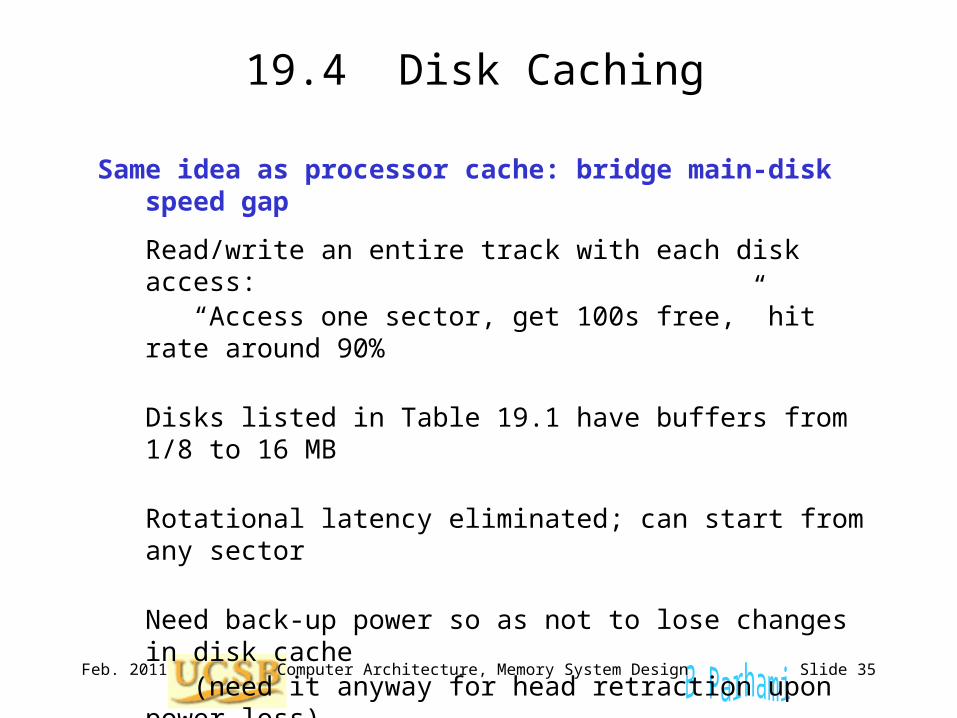
19.4 Disk Caching
Same idea as processor cache: bridge main-disk speed gap
Read/write an entire track with each disk access:“Access one sector, get 100s free,” hit rate around
90%
Disks listed in Table 19.1 have buffers from 1/8 to 16 MB
Rotational latency eliminated; can start from any sector
Need back-up power so as not to lose changes in disk cache(need it anyway for head retraction upon power loss)

Computer Architecture, Memory System DesignFeb. 2011 Slide 36
19.5 Disk Arrays and RAID
The need for high-capacity, high-throughput secondary (disk) memory
Processor speed
RAM size
Disk I/O rate
Number of disks
Disk capacity
Number of disks
1 GIPS 1 GB 100 MB/s
1 100 GB 1
1 TIPS 1 TB 100 GB/s 1000 100 TB 100
1 PIPS 1 PB 100 TB/s 1 Million 100 PB 100 000
1 EIPS 1 EB 100 PB/s 1 Billion 100 EB 100 Million
Amdahl’s rules of thumb for system balance
1 RAM bytefor each IPS
100 disk bytesfor each RAM byte
1 I/O bit per secfor each IPS

Computer Architecture, Memory System DesignFeb. 2011 Slide 37
Redundant Array of Independent Disks (RAID)
Fig. 19.5 RAID levels 0-6, with a simplified view of data organization.
RAID0: Multiple disks for higher data rate; no redundancy
RAID1: Mirrored disks
RAID2: Error-correcting code
RAID3: Bit- or byte-level striping with parity/checksum disk
RAID4: Parity/checksum applied to sectors,not bits or bytes
RAID5: Parity/checksum distributed across several disks
Data organization on multiple disks
Data disk 0
Data disk 1
Mirror disk 1
Data disk 2
Mirror disk 2
Data disk 0
Data disk 2
Data disk 1
Data disk 3
Mirror disk 0
Parity disk
Spare disk
Spare disk
Data 0
Data 1
Data 2
Data 0’
Data 1’
Data 2’
Data 0”
Data 1”
Data 2”
Data 0’”
Data 1’”
Data 2’”
Parity 0
Parity 1
Parity 2
Spare disk
Data 0
Data 1
Data 2
Data 0’
Data 1’
Data 2’
Data 0’”
Parity 1
Data 2”
Parity 0
Data 1’”
Data 2’”
Data 0”
Data 1”
Parity 2
RAID6: Parity and 2nd check distributed across several disks
A B C D P = 0 B = A C D P
A B C D P

Computer Architecture, Memory System DesignFeb. 2011 Slide 38
RAID Product Examples
IBM ESS Model 750

Computer Architecture, Memory System DesignFeb. 2011 Slide 39
19.6 Other Types of Mass Memory
Fig. 3.12 Magnetic and optical disk memory units.
(a) Cutaway view of a hard disk drive (b) Some removable storage media
Typically 2-9 cm
Floppy disk
CD-ROM
Magnetic tape
cartridge
. .
. . . . . .
Flash driveThumb driveTravel drive

Computer Architecture, Memory System DesignFeb. 2011 Slide 40
Fig. 19.6 Simplified view of recording format and access mechanism for data on a CD-ROM or DVD-ROM.
Optical Disks
Protective coating Substrate
Pits
Laser diode
Detector
Lenses Side view of
one track
Tracks
Beam splitter
Pits on adjacent
tracks
1 0 1 0 0 1 1 0
Spiral, rather than concentric, tracks

Computer Architecture, Memory System DesignFeb. 2011 Slide 41
Automated Tape Libraries

Computer Architecture, Memory System DesignFeb. 2011 Slide 42
20 Virtual Memory and Paging
Managing data transfers between main & mass is cumbersome• Virtual memory automates this process• Key to virtual memory’s success is the same as for cache
Topics in This Chapter
20.1 The Need for Virtual Memory
20.2 Address Translation in Virtual Memory
20.4 Page Placement and Replacement
20.6 Improving Virtual Memory Performance

Computer Architecture, Memory System DesignFeb. 2011 Slide 43
20.1 The Need for Virtual Memory
Fig. 20.1 Program segments in main memory and on disk.
Program and data on several disk tracks
System
Stack
Active pieces of program and data in memory
Unused space

Computer Architecture, Memory System DesignFeb. 2011 Slide 44
Fig. 20.2 Data movement in a memory hierarchy.
Memory Hierarchy: The Big Picture
Pages Lines
Words
Registers
Main memory
Cache
Virtual memory
(transferred explicitly
via load/store) (transferred automatically
upon cache miss) (transferred automatically
upon page fault)

Computer Architecture, Memory System DesignFeb. 2011 Slide 45
20.2 Address Translation in Virtual Memory
Fig. 20.3 Virtual-to-physical address translation parameters.
Virtual address
Physical address
Physical page number
Virtual page number Offset in page
Offset in page
Address translation
P bits
P bits
V P bits
M P bits

Computer Architecture, Memory System DesignFeb. 2011 Slide 46
Page Tables and Address Translation
Fig. 20.4 The role of page table in the virtual-to-physical address translation process.
Page table
Main memory
Valid bits
Page table register
Virtual page
number
Other f lags

Computer Architecture, Memory System DesignFeb. 2011 Slide 47
20.4 Page Replacement Policies
Least-recently used (LRU) policy
Implemented by maintaining a stack
Pages A B A F B E A
LRU stackMRU D A B A F B E A
B D A B A F B EE B D D B A F B
LRU C E E E D D A F

Computer Architecture, Memory System DesignFeb. 2011 Slide 48
20.6 Improving Virtual Memory Performance
Table 20.1 Memory hierarchy parameters and their effects on performance
Parameter variation Potential advantages Possible disadvantages
Larger main or cache size
Fewer capacity misses Longer access time
Larger pages or longer lines
Fewer compulsory misses (prefetching effect)
Greater miss penalty
Greater associativity (for cache only)
Fewer conflict misses Longer access time
More sophisticated replacement policy
Fewer conflict misses Longer decision time, more hardware
Write-through policy (for cache only)
No write-back time penalty, easier write-miss handling
Wasted memory bandwidth, longer access time

Computer Architecture, Memory System DesignFeb. 2011 Slide 49
Fig. 20.2 Data movement in a memory hierarchy.
Summary of Memory Hierarchy
Pages Lines
Words
Registers
Main memory
Cache
Virtual memory
(transferred explicitly
via load/store) (transferred automatically
upon cache miss) (transferred automatically
upon page fault)
Cache memory: provides illusion of very high speed
Virtual memory: provides illusion of very large size
Main memory: reasonable cost, but slow & small
Locality makes the illusions work
Recommended


![[XLS] · Web view005B PC Memory - 4MB 005C PC Memory - 6MB 005D PC Memory - 8MB 005E PC Memory - 10MB 005F PC Memory - 12MB 005G PC Memory - 14MB 005H PC Memory - 16MB 005I PC Memory](https://img.pdfslide.net/doc/110x75/5ab13df97f8b9ac66c8c4031/xls-view005b-pc-memory-4mb-005c-pc-memory-6mb-005d-pc-memory-8mb-005e-pc.jpg)