Features and Benefits▪ No external sense resistor required; single package solution▪ Reduced Power Loss:▫ 0.6 mΩ internal conductor resistance on EX package▫ 1.2 mΩ internal conductor resistance on LC package
▪ Economical low- and high-side current sensing▪ Output voltage proportional to AC or DC currents ▪ ±12.5 A and ±25 A full scale sensing ranges on LC package▪ ±15.5 A and ±31 A full scale sensing ranges on EX package▪ Overcurrent F A U L T trips and latches at 100% of full-scale current▪ Low-noise analog signal path▪ 100 kHz bandwidth▪ Small footprint, low-profile SOIC8 and QFN packages▪ 3.0 to 5.5 V, single supply operation ▪ Integrated electrostatic shield for output stability▪ Factory-trimmed for accuracy▪ Extremely stable output offset voltage▪ Zero magnetic hysteresis▪ Ratiometric output from supply voltage
DescriptionThe Allegro™ ACS711 provides economical and precise solutions for AC or DC current sensing in <100 V audio, communications systems, and white goods. The device package allows for easy implementation by the customer. Typical applications include circuit protection, current monitoring, and motor and inverter control.
The device consists of a linear Hall sensor circuit with a copper conduction path located near the surface of the die. Applied current flowing through this copper conduction path generates a magnetic field which is sensed by the integrated Hall IC and converted into a proportional voltage. Device accuracy is optimized through the close proximity of the magnetic signal to the Hall transducer.
The output of the device has a positive slope proportional to the current flow from IP+ to IP– (pins 1 and 2, to pins 3 and 4). The internal resistance of this conductive path is 0.6 mΩ for the EX package, and 1.2 mΩ for the LC package, providing a non-intrusive measurement interface that saves power in applications that require energy efficiency.
The ACS711 is optimized for low-side current sensing applications, although the terminals of the conductive path are electrically isolated from the sensor IC leads, providing sufficient internal creepage and clearance dimensions for a low AC or DC working voltage applications. The thickness
IP+IP+
IP–IP–
IP
GND
ACS711
+3.3 V
VIOUT
VCC CBYP0.1 μF
CLOADRPU
FAULT
ACS711
ACS711A-DS, Rev. 2
Hall Effect Linear Current Sensor with Overcurrent Fault Output for <100 V Isolation Applications
Continued on the next page…
Approximate Scale 1:1
Packages:
Typical Application
8-pin SOICNwith internally fused path
(LC package)
12-contact QFN3 mm × 3 mm × 0.75 mm
(EX package)
Application 1. The ACS711 outputs an analog signal, VIOUT , that varies linearly with the bi-directional AC or DC primary current, IP , within the range specified. The F A U ¯L T pin trips when IP reaches ±100% of its full-scale current.

Hall Effect Linear Current Sensor with Overcurrent Fault Output for < 100 V Isolation ApplicationsACS711
2Allegro MicroSystems, LLC115 Northeast CutoffWorcester, Massachusetts 01615-0036 U.S.A.1.508.853.5000; www.allegromicro.com
Absolute Maximum RatingsCharacteristic Symbol Notes Rating Units
Supply Voltage VCC 7 V
Reverse Supply Voltage VRCC –0.1 V
Output Voltage VIOUT 7 V
Reverse Output Voltage VRIOUT –0.1 V
Working Voltage for Basic Isolation VWORKING Voltage applied between pins 1-4 and 5-8 100 VAC peak or VDC
F A U ¯L T Pin Voltage VFAULT 7 V
Overcurrent Transient Tolerance IPOC 1 pulse, 100 ms 100 A
Nominal Operating Ambient Temperature TARange E –40 to 85 ºC
Range K –40 to 125 ºC
Maximum Junction Temperature TJ(max) 165 ºC
Storage Temperature Tstg –65 to 170 ºC
Selection Guide
Part Number TA (°C)
Optimized Accuracy Range, IP
(A)
Sensitivity2, Sens (Typ)
(mV/A)Package Packing1
ACS711ELCTR-12AB-T –40 to 85 ±12.5 110
8-pin SOICN 3000 pieces/reelACS711KLCTR-12AB-T –40 to 125
ACS711ELCTR-25AB-T –40 to 85 ±25 55
ACS711KLCTR-25AB-T –40 to 125
ACS711EEXLT-15AB-T3 –40 to 85 ±15.5 90
12-contact QFN with fused current loop 1500 pieces/reel
ACS711KEXLT-15AB-T3 –40 to 125
ACS711EEXLT-31AB-T3 –40 to 85 ±31 45
ACS711KEXLT-31AB-T3 –40 to 1251Contact Allegro for additional packing options.2Sensitivity measured with VCC = 3.3 V.3QFN package not qualified for automotive applications.
of the copper conductor allows survival of the device at up to 5× overcurrent conditions.
The ACS711 is provided in small, surface mount packages: SOIC8 and QFN12. The leadframe is plated with 100% matte tin, which is compatible with standard lead (Pb) free printed circuit board
assembly processes. Internally, the device is Pb-free, except for flip-chip high-temperature Pb-based solder balls, currently exempt from RoHS. The device is fully calibrated prior to shipment from the factory.
Description (continued)

Hall Effect Linear Current Sensor with Overcurrent Fault Output for < 100 V Isolation ApplicationsACS711
3Allegro MicroSystems, LLC115 Northeast CutoffWorcester, Massachusetts 01615-0036 U.S.A.1.508.853.5000; www.allegromicro.com
VCC
VIOUT
240 kΩ
FAULT
GND
Dyn
amic
Offs
et
Can
cella
tion
IP+
IP+
IP
IP
SensitivityTrim
SignalRecovery
Power-onReset
D
Reset
Master CurrentSupply
Sensitivity Temperature
Coefficient Trim
To all subcircuits Current FaultComparator
0 AmpereOffset Adjust
Hall CurrentDrive
CLOAD
CBYP RPU
VCC
IP+
IP+
IP–
IP–
VCC
VIOUT
FAULT
GND
1
2
3
4
8
7
6
5
10
9
8
7
1
2
3
4
5 6
12 11
VC
C
VIO
UT
GN
D
FAU
LT
NC
NC
NC
NC
IP+
IP+
IP–
IP–
Terminal List Table
NameNumber
DescriptionEX LC
GND 5 5 Signal ground terminal
F A U ¯L T 6 6 Overcurrent fault; active low
IP– 3 and 4 3 and 4 Terminals for current being sensed; fused internally
IP+ 1 and 2 1 and 2 Terminals for current being sensed; fused internally
NC 7, 8, 9, 10 – No connection
VCC 12 8 Device power supply terminal
VIOUT 11 7 Analog output signal
Functional Block Diagram
Pin-out Diagrams
LC PackageEX Package

Hall Effect Linear Current Sensor with Overcurrent Fault Output for < 100 V Isolation ApplicationsACS711
4Allegro MicroSystems, LLC115 Northeast CutoffWorcester, Massachusetts 01615-0036 U.S.A.1.508.853.5000; www.allegromicro.com
COMMON OPERATING CHARACTERISTICS Valid across the full range of TA for the LC package and at TA = 25°C for the EX package, VCC = 3.3 V, unless otherwise specified
Characteristic Symbol Test Conditions Min. Typ. Max. UnitsELECTRICAL CHARACTERISTICS
Supply Voltage1 VCC 3 3.3 5.5 V
Supply Current ICC VCC = 3.3 V, output open – 4 5.5 mA
Output Capacitance Load CLOAD VIOUT to GND – – 1 nF
Output Resistive Load RLOAD VIOUT to GND 15 – – kΩ
Primary Conductor Resistance RIP
EX package – 0.6 – mΩ
LC package, TA = 25°C – 1.2 – mΩ
VIOUT Rise Time tr IP = IPMAX, TA = 25°C, COUT = open – 3.5 – μs
Propagation Delay Time tPROP IP = IP(max), TA = 25°C, COUT = open – 1.2 – μs
Response Time tRESPONSE IP = IP(max), TA = 25°C, COUT = open – 4.6 – μs
Internal Bandwidth2 BWI –3 dB, TA = 25°C – 100 – kHz
Nonlinearity ELIN Over full range of IP – ±1 – %
Symmetry ESYM Apply full scale IP – 100 – %
VIOUT Saturation VoltagesVIOH
VCC – 0.3 – – V
VIOL – – 0.3 V
Quiescent Output Voltage VIOUT(Q) IP = 0 A, TA = 25°C – VCC / 2 – V
Power-On Time tPOOutput reaches 90% of steady-state level, TA = 25°C,20 A present on primary conductor – 35 – μs
F A U ¯L T Pin CharacteristicsF A U ¯L T Operating Point IFAULT – ± 1 x IP – A
F A U ¯L T Output Pullup Resistor RPU 1 – – kΩ
F A U ¯L T Output VoltageVOH – VCC–
0.3 – V
VOL RPU = 1 kΩ – 0.3 – V
F A U ¯L T Response Time tFAULT Measured from | IP | > | IFAULT | to VFAULT ≤ VOL – 1.3 – μs
VCC Off Voltage Level for Fault Reset3 VCCFR – – 200 mV
VCC Off Duration for Fault Reset3 tCCFR 100 – – μs
1Devices are programmed for maximum accuracy at 3.3 V VCC levels. The device contains ratiometry circuits that accurately alter the 0 A Output Voltage and Sensitivity level of the device in proportion to the applied VCC level. However, as a result of minor nonlinearities in the ratiometry circuit additional output error will result when VCC varies from the 3.3 V VCC level. Customers that plan to operate the device from a 5 V regulated supply should contact their local Allegro sales representative regarding expected device accuracy levels under these bias conditions.2Calculated using the formula BWI = 0.35 / tr.3After the F A U ¯L T pin is latched low, the only way to reset it is through a power-off and power-on cycle on the VCC pin. For fault reset, VCC must stay below VCCFR for a period greater than tCCFR before settling to the normal operation voltage (3 to 5.5 V).

Hall Effect Linear Current Sensor with Overcurrent Fault Output for < 100 V Isolation ApplicationsACS711
5Allegro MicroSystems, LLC115 Northeast CutoffWorcester, Massachusetts 01615-0036 U.S.A.1.508.853.5000; www.allegromicro.com
x12AB PERFORMANCE CHARACTERISTICS for LC package and E Temperature Range1 TA = 25°C and VCC = 3.3 V, unless otherwise specified
Characteristic Symbol Test Conditions Min. Typ. Max. UnitsOptimized Accuracy Range IP –12.5 – 12.5 A
Sensitivity SensOver full range of IP – 110 – mV/AFull scale of IP applied for 5 ms, TA = –40°C to 25°C – 110 – mV/AFull scale of IP applied for 5 ms, TA = 25°C to 85°C – 110 – mV/A
Noise2 VNOISE TA = 25 °C, no external low pass filter on VIOUT – 11 – mV
Electrical Offset VoltageVOE(TA) IP = 0 A, TA = 25°C – ±5 – mV
VOE(TOP)HT IP = 0 A, TA = 25°C to 85°C – ±40 – mVVOE(TOP)LT IP = 0 A, TA = –40°C to 25°C – ±50 – mV
Total Output Error3 ETOT IP = ±12.5 A,TA = –40°C to 85°C – ±5 – %1See Characteristic Performance Data for parameter distributions over temperature.2±3 sigma noise voltage.3Percentage of IP, with IP = ±12.5 A.
x12AB PERFORMANCE CHARACTERISTICS for LC package and K Temperature Range1TA = 25°C and VCC = 3.3 V, unless otherwise specified
Characteristic Symbol Test Conditions Min. Typ. Max. UnitsOptimized Accuracy Range IP –12.5 – 12.5 A
Sensitivity SensOver full range of IP – 110 – mV/AFull scale of IP applied for 5 ms, TA = –40°C to 25°C – 110 – mV/AFull scale of IP applied for 5 ms, TA = 25°C to 125°C – 110 – mV/A
Noise2 VNOISE TA = 25 °C, no external low pass filter on VIOUT – 11 – mV
Electrical Offset VoltageVOE(TA) IP = 0 A, TA = 25°C – ±5 – mV
VOE(TOP)HT IP = 0 A, TA = 25°C to 125°C – ±40 – mVVOE(TOP)LT IP = 0 A, TA = –40°C to 25°C – ±50 – mV
Total Output Error3 ETOT IP = ±12.5 A,TA = –40°C to 125°C – ±5 – %1See Characteristic Performance Data for parameter distributions over temperature.2±3 sigma noise voltage.3Percentage of IP, with IP = ±12.5 A.
x15AB PERFORMANCE CHARACTERISTICS1 TA = 25°C and VCC = 3.3 V, unless otherwise specified
Characteristic Symbol Test Conditions Min. Typ. Max. UnitsOptimized Accuracy Range IP –15.5 – 15.5 ASensitivity Sens Across full range of IP – 90 – mV/ANoise2 VNOISE No external low pass filter on VIOUT – 11 – mV
Electrical Offset VoltageVOE(TA) IP = 0 A – ±5 – mV
VOE(TOP)HT IP = 0 A, TA = 25°C to TA(max) – ±40 – mVVOE(TOP)LT IP = 0 A, TA = –40°C to 25°C – ±50 – mV
Total Output Error3 ETOT IP = ±12.5 A,TA = –40°C to TA(max) – ±5 – %1See Characteristic Performance Data for parameter distributions across the full temperature range.2±3 sigma noise voltage.3Percentage of IP, with IP = ±15.5 A.

Hall Effect Linear Current Sensor with Overcurrent Fault Output for < 100 V Isolation ApplicationsACS711
6Allegro MicroSystems, LLC115 Northeast CutoffWorcester, Massachusetts 01615-0036 U.S.A.1.508.853.5000; www.allegromicro.com
x25AB PERFORMANCE CHARACTERISTICS for LC package and K Temperature Range1TA = 25°C and VCC = 3.3 V, unless otherwise specified
Characteristic Symbol Test Conditions Min. Typ. Max. UnitsOptimized Accuracy Range IP –25 – 25 A
Sensitivity SensOver full range of IP – 55 – mV/AFull scale of IP applied for 5 ms, TA = –40°C to 25°C – 55 – mV/AFull scale of IP applied for 5 ms, TA = 25°C to 125°C – 55 – mV/A
Noise2 VNOISE TA = 25 °C, no external low pass filter on VIOUT – 8 – mV
Electrical Offset VoltageVOE(TA) IP = 0 A, TA = 25°C – ±5 – mV
VOE(TOP)HT IP = 0 A, TA = 25°C to 125°C – ±30 – mVVOE(TOP)LT IP = 0 A, TA = –40°C to 25°C – ±35 – mV
Total Output Error3 ETOT IP =±25 A, TA = –40°C to 125°C – ±4 – %1See Characteristic Performance Data for parameter distributions over temperature.2±3 sigma noise voltage.3Percentage of IP, with IP = ±25 A.
x25AB PERFORMANCE CHARACTERISTICS for for LC package and E Temperature Range1TA = 25°C and VCC = 3.3 V, unless otherwise specified
Characteristic Symbol Test Conditions Min. Typ. Max. UnitsOptimized Accuracy Range IP –25 – 25 A
Sensitivity SensOver full range of IP – 55 – mV/AFull scale of IP applied for 5 ms, TA = –40°C to 25°C – 55 – mV/AFull scale of IP applied for 5 ms, TA = 25°C to 85°C – 55 – mV/A
Noise2 VNOISE TA = 25 °C, no external low pass filter on VIOUT – 8 – mV
Electrical Offset VoltageVOE(TA) IP = 0 A, TA = 25°C – ±5 – mV
VOE(TOP)HT IP = 0 A, TA = 25°C to 85°C – ±30 – mVVOE(TOP)LT IP = 0 A, TA = –40°C to 25°C – ±35 – mV
Total Output Error3 ETOT IP =±25 A, TA = –40°C to 85°C – ±4 – %1See Characteristic Performance Data for parameter distributions over temperature.2±3 sigma noise voltage.3Percentage of IP, with IP = ±25 A.
x31AB PERFORMANCE CHARACTERISTICS1TA = 25°C and VCC = 3.3 V, unless otherwise specified
Characteristic Symbol Test Conditions Min. Typ. Max. UnitsOptimized Accuracy Range IP –31 – 31 ASensitivity Sens Across full range of IP – 45 – mV/ANoise2 VNOISE No external low pass filter on VIOUT – 8 – mV
Electrical Offset VoltageVOE(TA) IP = 0 A – ±5 – mV
VOE(TOP)HT IP = 0 A, TA = 25°C to TA(max) – ±30 – mVVOE(TOP)LT IP = 0 A, TA = –40°C to 25°C – ±35 – mV
Total Output Error3 ETOT IP =±25 A, TA = –40°C to TA(max) – ±4 – %1See Characteristic Performance Data for parameter distributions across the full temperature range.2±3 sigma noise voltage.3Percentage of IP, with IP = ±31 A.
Hall Effect Linear Current Sensor with Overcurrent Fault Output for < 100 V Isolation ApplicationsACS711
7Allegro MicroSystems, LLC115 Northeast CutoffWorcester, Massachusetts 01615-0036 U.S.A.1.508.853.5000; www.allegromicro.com
Thermal CharacteristicsCharacteristic Symbol Test Conditions1 Value Units
Package Thermal Resistance, Junction to Lead RθJL
LC package, mounted on Allegro ASEK 711 evalua-tion board 5 ºC/W
Package Thermal Resistance, Junction to Ambient2 RθJA
LC package, mounted on Allegro 85-0404 evaluation board, includes the power consumed by the board 23 ºC/W
EX package, mounted on Allegro 85-0528 evaluation board, includes the power consumed by the board 24 ºC/W
1Additional thermal information available on the Allegro website2The Allegro evaluation board has 1500 mm2 of 2 oz. copper on each side, connected to pins 1 and 2, and to pins 3 and 4, with thermal vias connecting the layers. Performance values include the power consumed by the PCB. Further details on the board are available from the Frequently Asked Questions document on our website.

Hall Effect Linear Current Sensor with Overcurrent Fault Output for < 100 V Isolation ApplicationsACS711
8Allegro MicroSystems, LLC115 Northeast CutoffWorcester, Massachusetts 01615-0036 U.S.A.1.508.853.5000; www.allegromicro.com
Characteristic Performance DataData taken using the ACS711KLC-12A, VCC = 3.3 V
MeanTypical Maximum Limit Typical Minimum Limit
80
60
40
20
0
-20
-40
-60–60 60 14080 100 120–40 40–20 200
–60 60 14080 100 120–40 40–20 200
–60 60 14080 100 120–40 40–20 200
–60 60 14080 100 120–40 40–20 200
–60 60 14080 100 120–40 40–20 200
2.0
1.5
1.0
0.5
0
-0.5
-1.0
-1.5
114
113
112
111
110
109
108
107
101.5
101.0
100.5
100.0
99.5
99.0
98.5
V OE
(mV)
E LIN
(%)
Sens
(mV/
A)
E SYM
(%)
TA (°C)TA (°C)
TA (°C)TA (°C)
8
6
4
2
0
-2
-4
-6
E TO
T (%
)
TA (°C)
I FA
ULT
(A)
TA (°C)
16
14
12
10
8
6
4
2
0–60 60 14080 100 120–40 40–20 200
Electrical Offset Voltage versus Ambient Temperature
Nonlinearity versus Ambient Temperature
Sensitivity versus Ambient Temperature
Symmetry versus Ambient Temperature
Total Output Error versus Ambient Temperature Fault Operating Point versus Ambient Temperature
Accuracy Data
Hall Effect Linear Current Sensor with Overcurrent Fault Output for < 100 V Isolation ApplicationsACS711
9Allegro MicroSystems, LLC115 Northeast CutoffWorcester, Massachusetts 01615-0036 U.S.A.1.508.853.5000; www.allegromicro.com
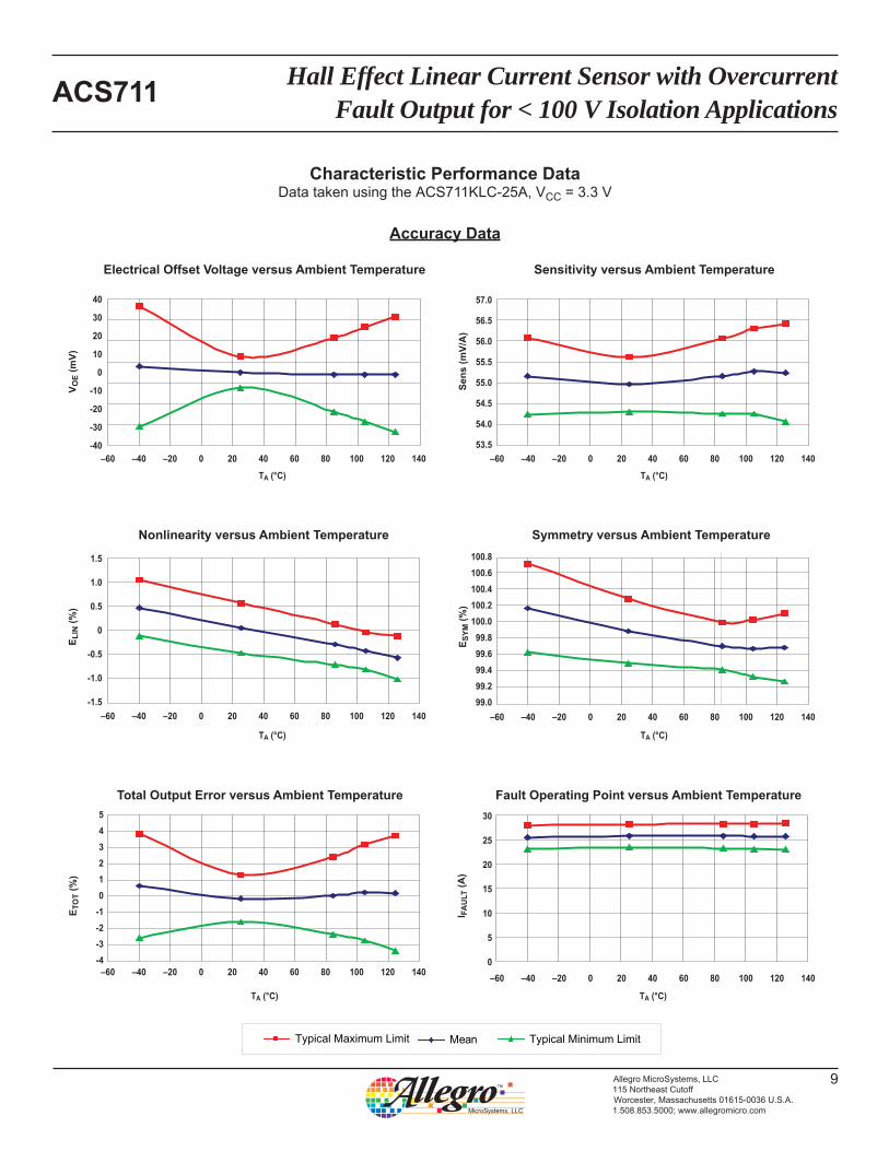
Characteristic Performance DataData taken using the ACS711KLC-25A, VCC = 3.3 V
Accuracy Data
MeanTypical Maximum Limit Typical Minimum Limit
40
30
20
10
0
-10
-20
-30
-40–60 60 14080 100 120–40 40–20 200
–60 60 14080 100 120–40 40–20 200
–60 60 14080 100 120–40 40–20 200
–60 60 14080 100 120–40 40–20 200
–60 60 14080 100 120–40 40–20 200
1.5
1.0
0.5
0
-0.5
-1.0
-1.5
57.0
56.5
56.0
55.5
55.0
54.5
54.0
53.5
100.8100.6100.4100.2100.099.899.699.499.299.0
V OE
(mV)
E LIN
(%)
Sens
(mV/
A)
E SYM
(%)
TA (°C)TA (°C)
TA (°C)TA (°C)
543210
-1-2-3-4
E TO
T (%
)
TA (°C)
I FA
ULT
(A)
TA (°C)
30
25
20
15
10
5
0–60 60 14080 100 120–40 40–20 200
Electrical Offset Voltage versus Ambient Temperature
Nonlinearity versus Ambient Temperature
Sensitivity versus Ambient Temperature
Symmetry versus Ambient Temperature
Total Output Error versus Ambient Temperature Fault Operating Point versus Ambient Temperature
Hall Effect Linear Current Sensor with Overcurrent Fault Output for < 100 V Isolation ApplicationsACS711
10Allegro MicroSystems, LLC115 Northeast CutoffWorcester, Massachusetts 01615-0036 U.S.A.1.508.853.5000; www.allegromicro.com
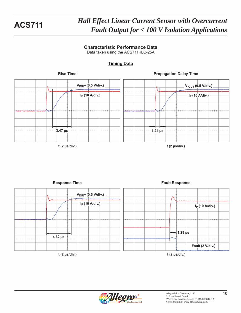
Characteristic Performance DataData taken using the ACS711KLC-25A
Timing Data
IP (10 A/div.)
3.47 μs
VIOUT (0.5 V/div.)
t (2 μs/div.)
IP (10 A/div.) IP (10 A/div.)
VIOUT (0.5 V/div.)
Fault (2 V/div.)
t (2 μs/div.) t (2 μs/div.)
IP (10 A/div.)
VIOUT (0.5 V/div.)
t (2 μs/div.)
4.62 μs1.28 μs
1.24 μs
Response Time
Propagation Delay Time
Fault Response
Rise Time

Hall Effect Linear Current Sensor with Overcurrent Fault Output for < 100 V Isolation ApplicationsACS711
11Allegro MicroSystems, LLC115 Northeast CutoffWorcester, Massachusetts 01615-0036 U.S.A.1.508.853.5000; www.allegromicro.com
Sensitivity (Sens). The change in sensor output in response to a 1 A change through the primary conductor. The sensitivity is the product of the magnetic circuit sensitivity (G / A) and the linear IC amplifier gain (mV/G). The linear IC amplifier gain is pro-grammed at the factory to optimize the sensitivity (mV/A) for the full-scale current of the device.
Noise (VNOISE). The product of the linear IC amplifier gain (mV) and the noise floor for the Allegro Hall effect linear IC. The noise floor is derived from the thermal and shot noise observed in Hall elements. Dividing the noise (mV) by the sensitivity (mV/A) pro-vides the smallest current that the device is able to resolve.
Linearity (ELIN). The degree to which the voltage output from the sensor varies in direct proportion to the primary current through its full-scale amplitude. Nonlinearity in the output can be attributed to the saturation of the flux concentrator approaching the full-scale current. The following equation is used to derive the linearity:
100 1– [{ [ {VIOUT_full-scale amperes – VIOUT(Q)Δ gain × % sat ( )2 (VIOUT_half-scale amperes – VIOUT(Q) )
where VIOUT_full-scale amperes = the output voltage (V) when the sensed current approximates full-scale ±IP .
Symmetry (ESYM). The degree to which the absolute voltage output from the sensor varies in proportion to either a positive or negative full-scale primary current. The following formula is used to derive symmetry:
100VIOUT_+ full-scale amperes – VIOUT(Q)
VIOUT(Q) – VIOUT –full-scale amperes Quiescent output voltage (VIOUT(Q)). The output of the sensor when the primary current is zero. For a unipolar supply voltage, it nominally remains at VCC ⁄ 2. Thus, VCC = 3.3 V translates into VIOUT(Q) = 1.65 V. Variation in VIOUT(Q) can be attributed to the resolution of the Allegro linear IC quiescent voltage trim and thermal drift.
Electrical offset voltage (VOE). The deviation of the device out-put from its ideal quiescent value of VCC / 2 due to nonmagnetic causes. To convert this voltage to amperes, divide by the device sensitivity, Sens.
Accuracy (ETOT). The accuracy represents the maximum devia-tion of the actual output from its ideal value. This is also known as the total ouput error. The accuracy is illustrated graphically in the output voltage versus current chart below.
Ratiometry. The ratiometric feature means that its 0 A output, VIOUT(Q), (nominally equal to VCC/2) and sensitivity, Sens, are proportional to its supply voltage, VCC . The following formula is used to derive the ratiometric change in 0 A output voltage,VIOUT(Q)RAT (%):
The ratiometric change in sensitivity, SensRAT (%), is defined as:
Definitions of Accuracy Characteristics
100VIOUT(Q)VCC / VIOUT(Q)3.3V
VCC / 3.3 V
100SensVCC / Sens3.3V
VCC / 3.3 V Output Voltage versus Sensed Current
Accuracy at 0 A and at Full-Scale Current
Increasing VIOUT (V)
+IP (A)
Accuracy
Accuracy
Accuracy25°C Only
Accuracy25°C Only
Accuracy25°C Only
Accuracy
0 A
v rO e Temp erature
AverageVIOUT
–IP (A)
v rO e Temp erature
v rO e Temp erature
Decreasing VIOUT (V)
IP(min)
IP(max) Full Scale

Hall Effect Linear Current Sensor with Overcurrent Fault Output for < 100 V Isolation ApplicationsACS711
12Allegro MicroSystems, LLC115 Northeast CutoffWorcester, Massachusetts 01615-0036 U.S.A.1.508.853.5000; www.allegromicro.com
Definitions of Dynamic Response Characteristics
Primary Current
Transducer Output
90
100
I (%)
Rise Time, trt
Rise time (tr). The time interval between a) when the sensor reaches 10% of its full scale value, and b) when it reaches 90% of its full scale value. The rise time to a step response is used to derive the bandwidth of the current sensor, in which ƒ(–3 dB) = 0.35 / tr. Both tr and tRESPONSE are detrimentally affected by eddy current losses observed in the conductive IC ground plane.
Power-On Time (tPO). When the supply is ramped to its operat-ing voltage, the device requires a finite time to power its internal components before responding to an input magnetic field.Power-On Time, tPO , is defined as the time it takes for the output voltage to settle within ±10% of its steady state value under an applied magnetic field, after the power supply has reached its minimum specified operating voltage, VCC(min), as shown in the chart at right.

Hall Effect Linear Current Sensor with Overcurrent Fault Output for < 100 V Isolation ApplicationsACS711
13Allegro MicroSystems, LLC115 Northeast CutoffWorcester, Massachusetts 01615-0036 U.S.A.1.508.853.5000; www.allegromicro.com
Application Information
LayoutTo optimize thermal and electrical performance, the following features should be included in the printed circuit board:
• The primary leads should be connected to as much copper area as is available.
• The copper should be 2 oz. or heavier.
• Additional layers of the board should be used for conducting the primary current if possible, and
should be connected using the arrangement of vias shown below.
• The two solder pads at the ends of the exposed pad loop should be placed directly on the copper trace that conducts the primary current.
• When using vias under exposed pads, such as with the EX package, using plugged vias prevents wicking of the solder from the pad into the via during reflow. Whether or not to use plugged vias should be evalu-ated in the application.
Primary Current Trace
Via
Solder pads
Via under pad
Signal traces
Exposed pad loop
EX packagefootprint
Primary Current Trace
Suggested Layout. EX package shown.

Hall Effect Linear Current Sensor with Overcurrent Fault Output for < 100 V Isolation ApplicationsACS711
14Allegro MicroSystems, LLC115 Northeast CutoffWorcester, Massachusetts 01615-0036 U.S.A.1.508.853.5000; www.allegromicro.com
Package LC, 8-pin SOIC
CSEATINGPLANE
1.27 BSC
GAUGE PLANESEATING PLANE
A Terminal #1 mark area
B
Reference land pattern layout (reference IPC7351 SOIC127P600X175-8M); all pads a minimum of 0.20 mm from all adjacent pads; adjust as necessary to meet application process requirements and PCB layout tolerances
B
D
C
21
8
Branding scale and appearance at supplier discretion
CSEATINGPLANEC0.10
8X
0.25 BSC
1.04 REF
1.75 MAX
For Reference Only; not for tooling use (reference MS-012AA)Dimensions in millimetersDimensions exclusive of mold flash, gate burrs, and dambar protrusions Exact case and lead configuration at supplier discretion within limits shown
4.90 ±0.10
3.90 ±0.10 6.00 ±0.20
0.510.31 0.25
0.10
0.250.17
1.270.40
8°0°
N = Device part number T = Device temperature range P = Package Designator A = Amperage L = Lot number Belly Brand = Country of Origin
NNNNNNN
LLLLL
1
TPP-AAA
A
Standard Branding Reference View
21
8
PCB Layout Reference ViewC
0.65 1.27
5.60
1.75
Branded Face

Hall Effect Linear Current Sensor with Overcurrent Fault Output for < 100 V Isolation ApplicationsACS711
15Allegro MicroSystems, LLC115 Northeast CutoffWorcester, Massachusetts 01615-0036 U.S.A.1.508.853.5000; www.allegromicro.com
Package EX, 12-Contact QFNWith Fused Sensed Current Loop
0.30
Branded Face
1.00
1
12
0.50
0.70
0.85
1.27MIN
0.80MIN
2.90
2.05 REF
2.70C
CSEATINGPLANE
0.25 +0.05–0.07
0.40±0.10
0.50 BSC 0.75 ±0.05
3.00 BSC
3.00 BSC
D
D Coplanarity includes exposed current path and terminals
B
A Terminal #1 mark area
B Fused sensed current path
For reference only, not for tooling use (reference JEDEC MO-220WEEDexcept for fused current path) Dimensions in millimetersExact case and lead configuration at supplier discretion within limits shown
C Reference land pattern layout (reference IPC7351 QFN50P300X300X80-17W4M); All pads a minimum of 0.20 mm from all adjacent pads; adjust as necessary to meet application process requirements and PCB layout tolerances; when mounting on a multilayer PCB, thermal vias at the exposed thermal pad land can improve thermal dissipation (reference EIA/JEDEC Standard JESD51-5)
12
0.201.79
21
A
12
1
2
PCB Layout Reference View
C0.089X
Branding scale and appearance at supplier discretionE
E Standard Branding Reference View
N = Device part number Y = Last two digits of year of manufacture W = Week of manufacture L = Lot number
NNNNYYWWLLLL
1

Hall Effect Linear Current Sensor with Overcurrent Fault Output for < 100 V Isolation ApplicationsACS711
16Allegro MicroSystems, LLC115 Northeast CutoffWorcester, Massachusetts 01615-0036 U.S.A.1.508.853.5000; www.allegromicro.com
Revision HistoryRevision Revision Date Description of Revision
Rev. 2 July 18, 2013 Update characteristics tables references
Copyright ©2008-2013, Allegro MicroSystems, LLCAllegro MicroSystems, LLC reserves the right to make, from time to time, such de par tures from the detail spec i fi ca tions as may be required to
permit improvements in the per for mance, reliability, or manufacturability of its products. Before placing an order, the user is cautioned to verify that the information being relied upon is current.
Allegro’s products are not to be used in life support devices or systems, if a failure of an Allegro product can reasonably be expected to cause the failure of that life support device or system, or to affect the safety or effectiveness of that device or system.
The in for ma tion in clud ed herein is believed to be ac cu rate and reliable. How ev er, Allegro MicroSystems, LLC assumes no re spon si bil i ty for its use; nor for any in fringe ment of patents or other rights of third parties which may result from its use.
For the latest version of this document, visit our website:www.allegromicro.com
Recommended