AP 5301/8301Instrumental Methods of Analysis
and Laboratory
Final Review
(except XPS and AES)
Prof YU Kin Man
E-mail: [email protected]
Tel: 3442-7813
Office: P6422
1

2
Teaching and Learning Questionnaire
(TLQ) - Course-end Evaluation,
Semester A, 2016/17
Course-end teaching and learning evaluation
for Semester A, 2016/17 will be carried out from
31 October to 4 December 2016
Prof K. M. Yu
Prof Paul K. Chu
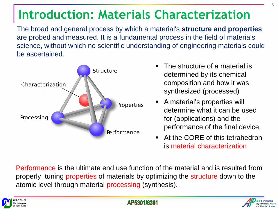
Introduction: Materials CharacterizationThe broad and general process by which a material's structure and properties
are probed and measured. It is a fundamental process in the field of materials
science, without which no scientific understanding of engineering materials could
be ascertained.
The structure of a material is
determined by its chemical
composition and how it was
synthesized (processed)
A material’s properties will
determine what it can be used
for (applications) and the
performance of the final device.
At the CORE of this tetrahedron
is material characterization
Performance is the ultimate end use function of the material and is resulted from
properly tuning properties of materials by optimizing the structure down to the
atomic level through material processing (synthesis).
3
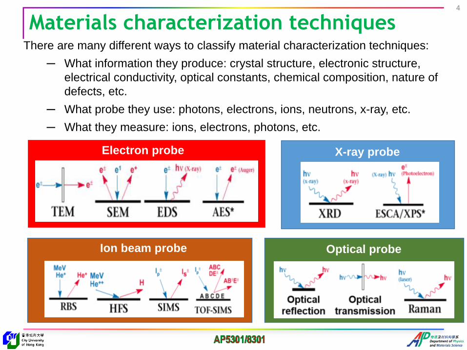
Materials characterization techniquesThere are many different ways to classify material characterization techniques:
─ What information they produce: crystal structure, electronic structure,
electrical conductivity, optical constants, chemical composition, nature of
defects, etc.
─ What probe they use: photons, electrons, ions, neutrons, x-ray, etc.
─ What they measure: ions, electrons, photons, etc.
4
Electron probe X-ray probe
Ion beam probe Optical probe
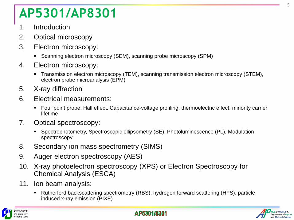
AP5301/AP83011. Introduction
2. Optical microscopy
3. Electron microscopy:
Scanning electron microscopy (SEM), scanning probe microscopy (SPM)
4. Electron microscopy:
Transmission electron microscopy (TEM), scanning transmission electron microscopy (STEM), electron probe microanalysis (EPM)
5. X-ray diffraction
6. Electrical measurements:
Four point probe, Hall effect, Capacitance-voltage profiling, thermoelectric effect, minority carrier lifetime
7. Optical spectroscopy:
Spectrophotometry, Spectroscopic ellipsometry (SE), Photoluminescence (PL), Modulation spectroscopy
8. Secondary ion mass spectrometry (SIMS)
9. Auger electron spectroscopy (AES)
10. X-ray photoelectron spectroscopy (XPS) or Electron Spectroscopy for Chemical Analysis (ESCA)
11. Ion beam analysis:
Rutherford backscattering spectrometry (RBS), hydrogen forward scattering (HFS), particle induced x-ray emission (PIXE)
5

6
SEM
TEM
SPM
XPS
AES
SIMS
RBS
EDS,WDS
EELSSTEM
diffraction
XRD
SAD
CBED
Spectro-
photometry
PL
SE
PR
4-pt
probe
Hall
CV/ECV
lifetime
OM
Microstructure
Crystalline defects
Mapping
Surface morphology
Elemental
composition
Depth profiles
Elemental mapping
Chemical bonding
Crystal structure
Chemical
compositionOptical properties
Band gap
Crystalline defects
Resistivity
Carrier conc.
Mobility
Minority carrier
lifetime
Dopant profiles
Chemical
analysis
AP5301/AP8301

Materials characterization: acronyms7
Microscopy
OM optical microscopy
NA numerical aperture
BF bright field
DF dark field
SCOM scanning confocal optical
microscopy
SEM scanning electron microscopy
SE secondary electron
BES backscattered electron
SPM scanning probe microscopy
STM scanning tunneling
microscopy
AFM atomic force microscopy
SNOM scanning near field optical
microscopy
TEM transmission electron
microscopy
SAD/ selected area electron
SAED diffraction
CBED convergent beam electron
diffraction
STEM scanning transmission
electron microscopy
EDS/ energy dispersive x-ray
EDX spectroscopy
X-ray techniques
WDS wavelength dispersive x-
ray spectroscopy
ADF annular dark field
imaging
HAADF high angle annular dark
field
EPMA electron probe
microanalysis
EELS electron energy loss
spectroscopy
XRF x-ray fluorescence
XRD x-ray diffraction
HRXRD high resolution x ray
diffraction
XAS x-ray absorption
XANES x-ray absorption near
edge structure
EXAFS extended x-ray
absorption fine structure
Electrical measurements
SRP spreading resistance
profiling
CV capacitance voltage
ECV electrochemical CV
Optical spectroscopy
SE spectroscopic ellipsometry
PL photoluminescence
PR photoreflectance
ER electroreflectance
TR thermoreflectance
Chemical analysis
SIMS secondary ion mass
spectrometry
ToF-SIMS time of flight SIMS
RBS Rutherford backscattering
spectrometry
HFS hydrogen forward
scattering
PIXE particle induced x-ray
emission
AES Auger electron
spectroscopy
SAM scanning Auger
microscopy
XPS x-ray photoelectron
spectroscopy
ARPES angle resolved
photoemission
spectroscopy

Optical vs. electron microscopy8
Microstructure of steel D2
(Metal Ravne Steel Selector)
Glass ceramic transmission microscope image
made with polarized light and full wave plate
Exfoliated molybdenum
disulfide on a perforated gridOptical Microscope
Electron Microscope
Atomic resolution TEM image of
nanocrystalline palladium. H. Rösner and C.
Kübel et al., Acta Mat., 2011, 59, 7380-7387.
Cross-section TEM image of MOCVD
grown InGaAs/GaAs quantum dot
superlattice solar cell (NREL)SEM micrographs of SMNb0.05%
Mat. Res. vol.6 no.2 São Carlos
Apr./June 2003.
Scanning electron microscopy (SEM) image
of as-grown p-type gallium nitride (p-GaN)
nanowire arrays on a silicon (111) substrate

Optical microscope9
Uses visible light as the
illumination source,
Has lateral resolution down to
0.1m
Used for almost all solids and
liquid crystals
Typically nondestructive
Mainly used for preliminary
direct visual observation
Microstructural features
observed: grains, precipitates,
inclusions, pores, whiskers,
defects, twin boundaries, etc.
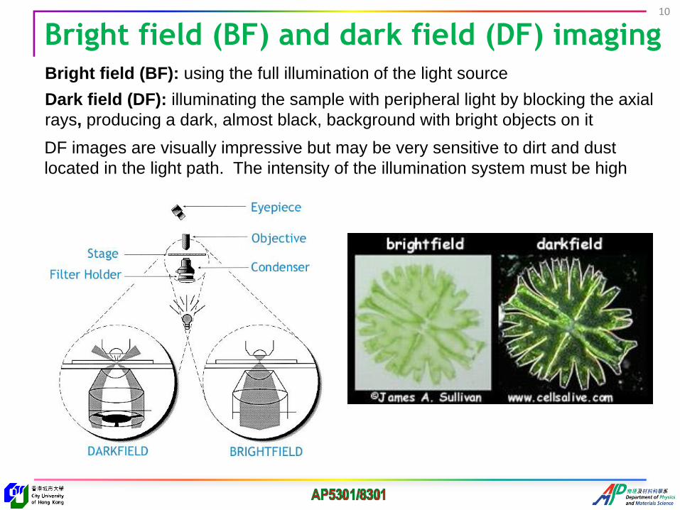
Bright field (BF) and dark field (DF) imagingBright field (BF): using the full illumination of the light source
Dark field (DF): illuminating the sample with peripheral light by blocking the axial
rays, producing a dark, almost black, background with bright objects on it
10
DF images are visually impressive but may be very sensitive to dirt and dust
located in the light path. The intensity of the illumination system must be high

Advanced optical microscopy11
Polarized light microscopy involves illumination of the
sample with polarized light for specimens that are visible
primarily due to their optically anisotropic
Phase contrast microscopy uses a special condenser
and objective lenses to convert phase differences (not
visible) into amplitude differences (visible)
Differential interference contrast (DIC) microscopy
enhances contrast by creating artificial shadows (pseudo
three-dimensional) using polarized light as if the object is
illuminated from the side
A fluorescence microscope uses fluorescence to
generate an image
─ Only allows observation of the specific structures
which have been labeled for fluorescence
Confocal microscopy adds a spatial pinhole at the
confocal plane to increase optical resolution and contrast
Scanning confocal optical microscopy (SCOM) is a
technique for obtaining high-resolution optical images with
depth selectivity. (a laser beam is used)
Blue-green Algae
Phase contrast DIC

Optical and electron microscopies: a comparison
Optical
microscopeTransmission electron
microscope (TEM)
Magneticlenses
detector
Light source Source of electrons
Condenser
Specimen
Objective
Eyepiece
Projector Specimen
Probe
scanning electron
microscope (TEM)
12

Electron beam microscopy/spectroscopy13
(1-50keV)
The types of signals produced by a SEM include secondary electrons (SEs),
back-scattered electrons (BSEs), characteristic X-rays and photons
(cathodoluminescence) (CL), absorbed current (specimen current) and
transmitted electrons. Both SEs and BSEs are used for imaging

Scanning electron microscopy
SEM has a large depth of field, producing an
image that is a good representation of the
three-dimensional sample
SEM produces images of high resolution at a
high magnification.
SEM usually also equipped with analytical
capability: electron probe microanalysis
(energy dispersive x-ray analysis).
The higher magnification, larger depth of field,
greater resolution and compositional and
crystallographic information makes the SEM
one of the most useful instruments in various
fields of research.
Magnification Depth of Field Resolution
OM 4 – 1000x 15.5 – 0.19m ~ 0.2m
SEM 10 – 3000000x 4mm – 0.4m 1-10nm
14

Secondary (SE) & backscattered (BSE) electrons15
SEs are low energy electrons (<50eV) produced
by inelastic interactions of high energy electrons
with core electrons
SE yield: 𝛿 = 𝑛𝑆𝐸/𝑛𝐵 >1 independent of Z but
depends on the angle of incidence. This gives rise
to topographic contrast of the specimen
Due to their low energy, only SE that are very
near the surface (<10nm) can exit the sample
and be examined (small escape depth).
Bright
Dark
BSE are produced by elastic
interactions (scatterings) of
electrons with nuclei of atoms and
they have high energy and large
escape depth
BSE yield: 𝜂 = 𝑛𝐵𝑆/𝑛𝐵 ~ increases
with atomic number, Z and thus can
be used to obtain images with
atomic number contrast
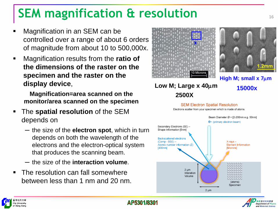
SEM magnification & resolution 16
Magnification in an SEM can be
controlled over a range of about 6 orders
of magnitude from about 10 to 500,000x.
Magnification results from the ratio of
the dimensions of the raster on the
specimen and the raster on the
display device,
Magnification=area scanned on the
monitor/area scanned on the specimen
The spatial resolution of the SEM
depends on
─ the size of the electron spot, which in turn
depends on both the wavelength of the
electrons and the electron-optical system
that produces the scanning beam.
─ the size of the interaction volume.
The resolution can fall somewhere
between less than 1 nm and 20 nm.
Low M; Large x 40m
High M; small x 7m
2500X15000x
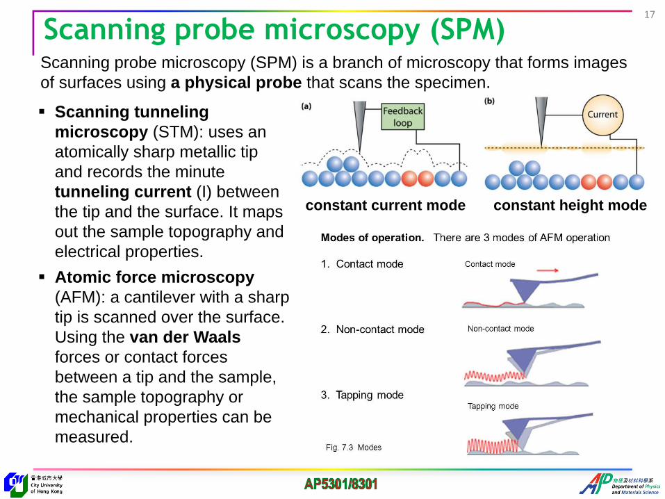
Scanning probe microscopy (SPM)17
Scanning probe microscopy (SPM) is a branch of microscopy that forms images
of surfaces using a physical probe that scans the specimen.
Scanning tunneling
microscopy (STM): uses an
atomically sharp metallic tip
and records the minute
tunneling current (I) between
the tip and the surface. It maps
out the sample topography and
electrical properties.
Atomic force microscopy
(AFM): a cantilever with a sharp
tip is scanned over the surface.
Using the van der Waals
forces or contact forces
between a tip and the sample,
the sample topography or
mechanical properties can be
measured.
constant current mode constant height mode

STM: modes of operation18
constant height modeconstant current mode
STMs use feedback to keep the
tunneling current constant by
adjusting the height of the scanner at
each measurement point
the voltage applied to the
piezoelectric scanner is adjusted to
increase/decrease the distance
between the tip and the sample
The image is then formed by plotting
the tip height vs. the lateral tip
position.
Tunneling current is monitored as
the tip is scanned parallel to the
surface.
There is a periodic variation in the
separation distance between the tip
and surface atoms.
A plot of the tunneling current vs.
tip position shows a periodic
variation which matches that of the
surface structure-a direct "image"
of the surface.

STM vs. AFM19
STM AFM
Measures local electron density of states,
not nuclear positions─not true topographic
imaging
Real topographic imaging
High lateral and vertical resolution –because
of the exponential dependence of the
tunneling current on distance
Lower lateral resolution
Exponential dependence between tunneling
current and distance
The force-distance dependence in AFM is
much more complex
Probe electronic properties (LDOS –
including spin states)
Probe various physical properties: magnetic,
electrostatic, hydrophobicity, friction, elastic
modulus, etc
Generally applicable only to conducting
(and semiconducting) samples
Applied to both conductors and insulators
Writing voltage and tip-to-substrate spacing
are integrally linked
Writing voltage and tip-to-substrate spacing
can be controlled independently

Control brightness,
convergence
Control contrast
A disc of metal
Transmission electron microscopy20

TEM operation21
TEM offers two methods of specimen observation, diffraction mode and image
mode. The objective lens forms a diffraction pattern in the back focal plane with
electrons scattered by the sample and combines them to generate an image in the
image plane.
Whether the diffraction pattern or the
image appears on the viewing screen
depends on the strength of the
intermediate lens.
The image mode produces an image of
the illuminated sample area
In image mode, the post-specimen lenses
are set to examine the information in the
transmitted signal at the image plane of
the objective lens.
There are three primary image modes
that are used in conventional TEM work,
bright-field microscopy, dark-field
microscopy, and high-resolution electron
microscopy.

Polycrystalline materials
The electron diffraction pattern is a set of rings, with some spots depending on
the crystallite sizes.
Nano to Amorphous materials
As the crystal size get smaller (nm) the
rings get more diffuse and eventually
become halo-like when the material
becomes amorphous
TEM: diffraction pattern
Al single crystalPolycrystalline Pt
silicide (PtSi)
Silicon with epitaxial nickel
silicides ( Si - NiSi - NiSi2)
Polycrystalline nickel mono
silicide (NiSi) on top of
single crystalline silicon
(Si).
Amorphous GaNAsnanocrystalline GaNAs
22

Advantages
TEMs offer very powerful magnification and resolution.
TEMs have a wide-range of applications and can be utilized in a variety of
different scientific, educational and industrial fields
TEMs provide information on element and compound structure.
Images are high-quality and detailed.
Chemical information with analytical attachments
Disadvantages
TEMs are large and very expensive (USD 300K to >1M)
Laborious sample preparation.
Operation and analysis requires special training.
Samples are limited to small size (mm) and must be electron transparent.
TEMs require special housing and maintenance.
Images are black and white .
TEM: advantages and disadvantages23

Comparison: SEM and TEM
TEM SEM
Electron beam Broad, static beam Beam focused to fine point and
scan over specimen
Electron path passes through thin specimen. scans over surface of specimen
Specimens Specially prepared thin
specimens supported on TEM
grids.
Sample can be any thickness and is
mounted on an aluminum stub.
Specimen stage Located halfway down column. At the bottom of the column.
Image formation Transmitted electrons collectively
focused by the objective lens and
magnified to create a real image
Beam is scanned along the surface
of the specimen to build up the
image
Image display On fluorescent screen. On TV monitor.
Image nature Image is a two dimensional
projection of the sample.
Image is of the surface of the
sample
Magnification Up to 5,000,000x ~250,000x
Resolution ~0.2 nm ~2-5 nm
24

Scanning Transmission Electron Microscopy (STEM)
The rastering of the beam across the
sample makes these microscopes
suitable for analysis techniques such
as mapping by
energy dispersive X-ray (EDX)
spectroscopy
electron energy loss
spectroscopy (EELS)
annular dark-field imaging
(ADF).
By using a high-angle detector
(high angle annular dark-field
HAADF), atomic resolution
images where the contrast is
directly related to the atomic
number (z-contrast image) can be
formed. SAED =0.26o or ~6.4 mrads
I Z2
25
X-rays
EDX detector
luminescence
In a STEM the electron beam is focused into a narrow spot which is scanned
over the sample in a rastering mode.

Electron probe microanalysis (EPMA)26
Energy-dispersive X-ray spectroscopy
(EDS, EDX, or XEDS) is an analytical
technique used for the elemental
analysis. In a SEM or STEM, the
incident electrons are used as the
excitation source creating characteristic
x-rays from different elements in the
target.
Electron energy loss spectroscopy
(EELS): Electrons lose energy through
inner-shell ionizations are useful for
detecting the elemental components of
a material
─ the detailed shape of the spectral
profiles gives information on the
electronic structure, chemical
bonding, and nearest neighbor
distances for each atomic species.
─ Quantitative elemental concentration
for the element 3≤𝑍≤35

EPMA: WDS vs EDS27
WDS EDS
Spectra acceptance One element/run Entire spectrum in one shot
Collection time > 10 mins Mins
Sensitive elements Better for lighter elements
(Be, B, C, N, O)
Resolution ~few eV ~130 eV
Probe size ~200 nm ~5 nm
Max count rate ~50000 cps <2000 cps
Detection limits 100 ppm 10000 ppm
Spectral artifacts rare Peak overlap

EPMA: EELS vs EDS28
EELS EDS
Energy resolution ~0.1 eV ~130 eV
Energy range 0-3000 eV 1-50 keV
Element range Better for light elements Better for heavy
elements
Ease of use Medium high
Spatial resolution Good beam broadening
Information Elemental, coordination,
bonding
Only elemental
Quantification Easy Easy
Peak overlap No Can be severe

X-ray powder diffraction29
X-ray powder diffraction (XRD) is a rapid analytical
technique primarily used for phase identification
of a crystalline material and can provide
information on unit cell dimensions.
The sample holder and the x-ray detector are
mechanically linked: the detector turns 2 when
the sample holder turns so that the detector is
always ready to detect the Bragg diffracted
beam 2d sin θ = 𝑛𝜆
Bragg-Brentano geometry
Applications:
Phase Composition of a Sample
Unit cell lattice parameters and Bravais lattice symmetry
Residual Strain (macrostrain)
Epitaxy/Texture/Orientation
Crystallite Size and Microstrain

XRD: alloy composition analysis30
ZnO is alloyed with ZnS to form
ZnO1-xSx alloy
Wurtzite ZnO (c=0.52 nm) and ZnS
(c=0.626 nm)
As x increases (more S substituting
in O sublattice), the lattice
parameter increases
Bragg law: 𝜆 = 2𝑑 sin 𝜃 increasing 𝑑means decreasing 𝜃.
Vegard's law: lattice parameter of a
solid solution of two constituents is
approximately equal to a rule of
mixtures of the two constituents'
lattice parameters
𝑐𝑍𝑛𝑂1−𝑥𝑆𝑥 = 𝑥𝑐𝑍𝑛𝑆 + (1 − 𝑥)𝑐𝑍𝑛𝑂
Composition 𝑥 can be derived from
the measured lattice parameter 𝑐.
Increasing x
(0002) Diffraction peaks of ZnO1-xSx alloy

XRD: crystallite size31
Crystallites smaller than ~120nm create broadening of diffraction peaks
this peak broadening can be used to quantify the average crystallite size of
nanoparticles using the Scherrer equation
─ contributions due to instrument broadening should be known by using
a standard sample (e.g. a single crystal)
Scherrer equation:
𝐵 2𝜃 =𝐾𝜆
𝐿 cos 𝜃
where B is the 2𝜃 FWHM
peak broadening in radian,
𝜆 is the wavelength of the x-
ray used, L is the grain size
and K~0.9

XRD: lattice strain32
No Strain
do
2
Uniform Strain: (d1-do)/do
d1
d strain
2Peak moves, no shape changes
Non-uniform StrainPeak broadens
Broadeing 2 2 tan
d
bd
2
d1constant

XRD: preferred orientation
Preferred orientation of crystallites can create a variation in diffraction peak
intensities that can be
qualitatively analyzed using a 1D diffraction pattern (powder pattern)
quantitatively analyzed by a pole figure which maps the intensity of a single
peak as a function of tilt and rotation of the sample
33

Resistivity: the four point probe34
The four point probe is commonly used to
determine the resistivity of semiconductor
samples (wafers)
The outer 2 probes are connected to a current
source
The two inner probes are high impedance
voltage sensors
The sample thickness 𝛿 is assumed to be
constant

Hall Effect35
The Hall coefficient for electrons is
𝑅𝐻 =ℰ𝐻,𝑒
𝐽𝑥𝐵= −
1
𝑛𝑒(negative)
For hole carriers: 𝑅𝐻 =ℰ𝐻,ℎ
𝐽𝑥𝐵=
1
𝑝𝑒(positive)
The Hall effect describes the behavior of
free carriers in a semiconductor when an
electric and a magnetic field are applied.
The van der Pauw method is a technique
commonly used to measure the resistivity and
the Hall coefficient of a sample of any arbitrary
shape
The free carrier concentration 𝑛 =1
𝑒𝑅𝐻is given by: 𝑛 =
1
𝛿
𝐵
𝑒∆𝑅24,13
With known resistivity and carrier concentration, the mobility is given by:
𝜇 =1
𝑛𝑒𝜌=2ln(2)
𝜋𝐵
∆𝑅24,13𝑅12,34 + 𝑅23,41
1
𝑓

Variable Temperature Hall Effect
At high temperature: Intrinsic
─ 𝑛𝑖 ∝ 𝑒−𝐸𝑔/2𝑘𝐵𝑇
─ slope=−𝐸𝑔
2𝑘𝐵𝑇
Medium Temperature: 𝑘𝐵𝑇 ≫ 𝐸𝑑─ Extrinsic or saturation regime
─ 𝑛 = 𝑁𝑑 − 𝑁𝑎
Low temperature: freeze out region
─ 𝑛 ∝ 𝑒−𝐸𝑑/2𝑘𝐵𝑇
─ slope=−𝐸𝑑
2𝑘𝐵𝑇(half slope)
─ At even lower temperature
𝑛 ∝ 𝑒−𝐸𝑑/𝑘𝐵𝑇 (full slope)
─ The concentration at which the half slope turns into full slop corresponds to 𝑁𝑎
For a semiconductor sample with both donors and acceptors 𝑁𝑑 𝑎𝑛𝑑 𝑁𝑎. A
variable temperature Hall effect measurement plotted as ln 𝑛 𝑣𝑠.1
𝑇─Arrhenius
plot can tell us a lot of information
T
Arrhenius Plot
Half slope
Full slope
Variable temperature Hall effect measurements provide a convenient way to obtain donor or acceptor binding energies.
36

Electrical measurements: a comparison37
4 point probe Hall effect CV ECV thermopower
Information
obtained
Resistivity Free carrier
concentration,
mobility
Net ionized dopant
concentration
Net ionized dopant
concentration
Seebeck coefficient
Conduction
type (n or p)
No Yes Yes Yes Yes
Sample size From mm to wafer 0.5 to 2 cm square 0.5 to 2 cm square >0.5 cm >0.5 cm
Depth
profiling
No No Yes Yes Mo
Destructive Somewhat No Need to form a
Schottky contact
Yes No
Equipment
cost
Low Low to high
(from <20kUSD to
>200k USD)
Low High
(>150k USD)
Low to medium

SpectrophotometrySpectrophotometry is the quantitative
measurement of the reflection or
transmission properties of a material as a
function of wavelength in the spectral
range of visible light (Vis), near-ultraviolet
(UV), and near-infrared (NIR). It is more
commonly called UV-Vis-NIR
spectroscopy.
38
Transmission and reflection data are
combined to find the absorption coefficient
𝛼 𝜆
𝐼𝑇(𝜆) = (𝐼𝑜 𝜆 − 𝐼𝑅(𝜆))𝑒−𝛼(𝜆)𝑥
𝛼 𝜆 =1
𝑥ln
𝐼𝑜 𝜆 − 𝐼𝑅(𝜆)
𝐼𝑇(𝜆)
From the absorption coefficient of a solid (thin
film), the electronic properties can be derived.
𝑥
𝐼𝑜
𝐼𝑅
𝐼𝑇

Optical Absorption Measurement𝑥
𝐼𝑜
𝐼𝑅
𝐼𝑇
ZnO thin film
𝛼 𝜆 =1
𝑥ln
𝐼𝑜 𝜆 − 𝐼𝑅(𝜆)
𝐼𝑇(𝜆)
𝛼hν 1/𝑛 = 𝐴 hν − 𝐸𝑔To determine if the material has a direct
or indirect gap
plot 𝛼hν 1/𝑛vs. hν Notice that we can linearly
extrapolate 𝛼hν 2vs. hν (𝑛 = 1/2) to
obtain a band gap 𝐸𝑔 = 3.3 𝑒𝑉
𝛼hν 1/2vs. hν (𝑛 = 2) does not result
in a straight line
ZnO is a direct gap material.
39

Spectroscopic ellipsometry (SE)
The measured signal is the change in polarization as the incident radiation (in a known state) interacts with the material structure of interest (reflected, absorbed, scattered, or transmitted).
The polarization change is quantified by the amplitude ratio, 𝚿, and the phase difference, 𝚫.
𝜌 =𝑅𝑝
𝑅𝑠= 𝑡𝑎𝑛Ψ𝑒𝑖Δ = 𝑓(𝒏𝒊, 𝒌𝒊, 𝒕𝒊)
𝑤ℎ𝑒𝑟𝑒𝑅𝑝
𝑅𝑠is the Fresnel reflection coefficient
𝑅𝑝 =𝐸𝑝(𝑟𝑒𝑓𝑙𝑒𝑐𝑡𝑒𝑑)
𝐸𝑝(𝑖𝑛𝑐𝑖𝑑𝑒𝑛𝑡); 𝑅𝑠 =
𝐸𝑠(𝑟𝑒𝑓𝑙𝑒𝑐𝑡𝑒𝑑)
𝐸𝑠(𝑖𝑛𝑐𝑖𝑑𝑒𝑛𝑡)
40
The sample has a
layered structure and
each layer 𝑖 has optical
constants (𝑛𝑖 , 𝑘𝑖) and a
thickness 𝑡𝑖 .

SE: advantages and limitations
Non-destructive technique
Film thickness measurement, can measure down to <1 nm
Can measure optical constants 𝑛 and 𝑘 for unknown materials
─ Absorption coefficient, band gap, carrier concentration, mobility, effective
mass, etc.
Can also measure film composition, porosity and roughness
Absolute measurement: do not need any reference.
Rapid measurement: get the full spectrum (190nm up1700nm) in few seconds
Can be used for in-situ analysis
Small equipment footprint: do not require a lot of lab space
Can only measure flat, parallel and reflecting surfaces
Some knowledge of the sample is required: number of layers, type of layers, etc.
SE is an indirect measurement: does not give directly the physical parameters
A realistic physical model of the sample is usually required to obtain useful
information
41

Photoluminescence42
Spectral feature Material parameter
Peak energy Compound identification
Band gap/electronic levels
Impurity or exciton binding energy
Quantum well width
Impurity species
Alloy composition
Internal strain
Fermi energy
Peak width Structural and chemical quality
Quantum well interface roughness
Carrier or doping density
Peak intensity Relative quantity
Polymer conformation
Relative efficiency
Surface damage
Excited state lifetime
Impurity or defect concentration

Photoreflectance: principles Changes in reflectivity
∆𝑅
𝑅can be related to the perturbation of the dielectric
function of the material, 휀 = 휀1 + 𝑖휀2:
∆𝑅
𝑅= 𝛼 휀1, 휀2 ∆휀1 + 𝛽 휀1, 휀2 ∆휀2
where 𝛼 and 𝛽 are the Seraphin coefficients, ∆휀1 and ∆휀2 represent
photo-induced changes of the real and imaginary parts of the dielectric
function, respectively.
43
The imaginary part 휀2 changes
slightly in electric field, resulting
in a sharp resonance ∆휀2 exactly
at the energy of the optical
transition.
It can be shown that in a case of
the bulk crystal, the shape of
dielectric function changes is of
the third derivative of the
unperturbed dielectric function.

Secondary ion mass spectrometry (SIMS)
SIMS is generally used for surface, bulk,
microanalysis, depth profiling, and impurity
analysis. The technique involves bombarding
the surface of a sample with a beam of ions,
thus emitting secondary ions. These ions are
later measured with a mass spectrometer to
determine either the elemental or isotopic
composition of the surface of the sample.
44
negative, positive, and neutral
charges with kinetic energies ranging
from zero to a few hundred eV.Cs+, O2+, Ar+ and Ga+
at energies ~ 1-30 keV
Sputtered species:
Monatomic and
polyatomic particles of
sample material (+ve,
-ve or neutral)
Re-sputtered primary
species (+ve, -ve or
neutral)
Electrons
photons

Secondary ion yields: primary ion beams
Oxygen works as a medium which strips off electrons from the speeding
sputtered atoms when they leave surface, while Cesium prefers to load an
electron on the sputtered atoms.
𝑶𝟐+ ions beam:
─ During secondary emission the Me-O
bonds break thus generating 𝑀𝑒𝑛+
𝑪𝒔+ ions beam:
─ Increased availability of electrons
leads to increased negative ion
formation especially for elements with
high electron affinity.
45
Secondary ion yield depends critically on the primary ion beam species. Typically
𝐶𝑠+and 𝑂2+ ion beams are used in SIMS measurements.
Selection of primary ions:
Inert gas (Ar, Xe, etc.)
─ Minimize chemical modification
Oxygen
─ Enhance positive ions
Cesium
─ Enhance negative ions
Liquid metal (Ga)
─ Small spot for enhanced
lateral resolution

SIMS: secondary ion yield46
Secondary ion current of species 𝑚
𝐼𝑠𝑚 = 𝐼𝑝𝑦𝑚𝛼
+𝜃𝑚𝜂
𝐼𝑝 = primary particle flux
𝑦𝑚 = sputter yield
𝛼+ = ionization probability to positive ions
𝜃𝑚 = fractional concentration of m in the layer
𝜂 = transmission of the analysis systemIon yield is influenced by
─ Matrix effects
─ Surface coverage of reactive elements
─ Background pressure
─ Orientation of crystallographic axes with respect to the sample surface
─ Angle of emission of detected secondary ions
The number of secondary particles (atoms/ions) emitted by the surface for each
impinging primary ion is defined as sputtering yield and can range between 5
and 15. The fraction of ionized emitted particles is called secondary ion yield
and ranges typically between 10-4 to 10-6.
In SIMS, it is the secondary ions that are eventually detected

SIMS: modes of operation47
Static SIMS: 0.1-10 keV ions are
employed, with current surface
densities in the nA/cm2 range,
Under these conditions the total
erosion of the sample first
monolayer (1 nm) may take even
an hour.
Dynamic-SIMS: 10-30 keV ions,
with current surface densities in
the A-mA/cm2 range, are used.
Under these conditions the sample
is eroded continuously and the
acquired mass spectra enable the
monitoring of constituting elements
along the sample depth (depth
profiling).
According to the primary ion energy and current, the SIMS technique can be
divided into two variants:
Profiling
Material removal
Elemental analysis
Ultra surface
analysis
Elemental or
molecular analysis
Analysis completed
before significant
fraction of molecules
destroyed

Static SIMS48
Positive ion TOF mass spectrum of polydimethylsiloxane
contaminated polyethylene terephthalateSilicon wafer contaminated with copper, iron and chromium
Range of elements H to U: all isotopes
Destructive Yes, if sputtered long enough
Chemical bonding Yes
Depth probed Outer 1 to 2 monolayers
Lateral resolution Down to below 100 nm
Imaging/mapping Yes
Quantification Possible with suitable standard
Mass range Typically up to 1000 amu, 10000 amu (ToF)
Main application Surface chemical analysis, organics, polymers

Dynamic SIMS49
Range of elements H to U: all isotopes
Destructive Yes, material removed during sputtering
Chemical bonding In rare cases only
Depth probed Depth resolution 2-30 nm, probe into m below surface
Quantification Standard needed
Accuracy 2%
Detection limits 1012-1016 atoms/cm3 (ppb-ppm)
Imaging/mapping Yes
Sample requirements Solid; vacuum compatible
Near surface B depth profiles
from a 2.2 keV BF implant in
Si using different energies O2+
primary beam

Comparison: static and dynamic SIMS50

SIMS can be used to determine the composition of organic and inorganic
solids at the outer 5 nm of a sample.
Can generate spatial or depth profiles of elemental or molecular
concentrations.
These profiles can be used for elemental mapping.
To detect impurities or trace elements, especially in semiconductors.
Secondary ion images have resolution on the order of 0.5 to 5 μm.
Detection limits for trace elements range between 1012 to 1016 atoms/cc.
Spatial resolution is determined by primary ion beam widths, which can be as
small as 100 nm.
SIMS: summary
SIMS is the most sensitive elemental and isotopic surface
microanalysis technique (bulk concentrations of impurities of around
1 part-per-billion). However, very expensive.
51

Advantages and weaknesses of SIMS
Advantages Weaknesses
Excellent sensitivity, especially for
light elements
Destructive method
High surface sensitivity Element specific selectivity
Depth profiling with excellent depth
resolution (nm) (dynamic)
Standards needed for quantification
Good spatial resolution (<1-25 m) Sample must be vacuum compatible
Small analyzed volume (down to
0.3m3) so little sample is needed
Sample mist have a flat surface
Information about the chemical
surface composition due to ion
molecules (static)
High equipment cost (>1M-3M USD)
Elements from H to U can be
detected with excellent mass
resolution
52

SIMS and other techniques
* = yes, with compensation for the effects of sample charging
Characteristic AES XPS SEM/EDS SIMS
Elemental range Li and higher Z Li and higher Z Na and higher Z All Z
Specificity Good Good Good Good
Quantification With calibration With calibration With calibration Correction
necessary
Detection limits
(atomic fraction)
10-2 to 10-3 10-2 to 10-3 10-3 to 10-8 10-3 to 10-8
Mass resolution element element element <isotope
Lateral resolution (m) 0.05 ~1000 0.05 1
Depth resolution (nm) 0.3-2.5 1-3 1000-50000 0.3-2
Organic samples No Yes Yes* Yes
Insulator samples Yes* Yes Yes* Yes*
Structural information Elemental Elemental and
Chemical
Elemental Elemental and
Chemical
Destructiveness Low
High (profiling)
Very Low
High (profiling)
Medium High(dynamic)
Medium(static)

Ion Beam Analysis: an overview
Incident Ions
Absorber foil
Elastic recoil detection
Rutherford backscattering
(RBS), resonant scattering,
channeling
Particle induced x-ray
emission (PIXE)
Nuclear Reaction Analysis
(NRA) p, , n, g
Ion Beam
Modification
Defects generation
Inelastic Elastic
54

RBS: basic concepts
Kinematic factor: elastic energy transfer from a projectile to a target
atom can be calculated from collision kinematics
mass determination
Scattering cross-section: the probability of the elastic collision
between the projectile and target atoms can be calculated
quantitative analysis of atomic composition
Energy Loss: inelastic energy loss of the projectile ions through the
target
perception of depth
These allow RBS analysis to give quantitative depth distribution of
targets with different masses
55

Strengths & weaknesses of RBS Simple in principle
Fast and direct
Quantitative without standard
Depth profiling without chemical or physical sectioning
Non-destructive
Wide range of elemental coverage
No special specimen preparation required
Can be applied to crystalline or amorphous materials
Simultaneous analysis with several ion beam techniques Poor lateral
resolution (~0.5-1mm)
Moderate depth resolution (>50Å)
No microstructural information
No phase identification
Poor mass resolution for target mass heavier than 70amu (PIXE)
Detection of light impurities more difficult
Data may not be obvious: require knowledge of the technique
56
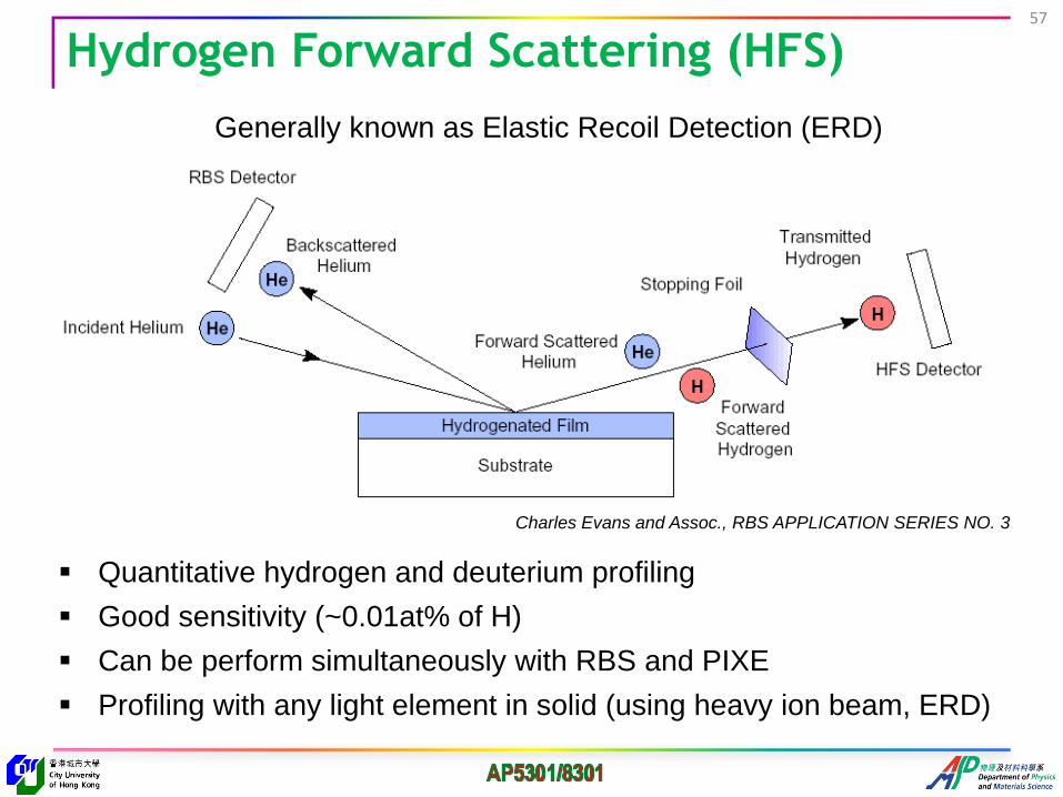
Hydrogen Forward Scattering (HFS)
Charles Evans and Assoc., RBS APPLICATION SERIES NO. 3
Quantitative hydrogen and deuterium profiling
Good sensitivity (~0.01at% of H)
Can be perform simultaneously with RBS and PIXE
Profiling with any light element in solid (using heavy ion beam, ERD)
Generally known as Elastic Recoil Detection (ERD)
57

Particle Induced X-ray Emission (PIXE)

Ion Channeling
Kobelco Steel Group
59

Channeling: Impurity Lattice Location
0 0.2 0.6 1.0Distance from atom row, r/ro
3
2
1
Flu
x
0.2
0.4
0.6
0.8y/y1
=1.0
0.0
Channel center
ro
r
Atomic row

Strengths of Ion Beam Analysis Techniques
Simple in principle
Fast and direct
Quantitative (without standard for RBS)
Depth profiling without chemical or physical sectioning
Non-destructive
Wide range of elemental coverage
No special specimen preparation required
Can be applied to crystalline or amorphous materials
Simultaneous analysis with various ion beam
techniques (RBS, PIXE, NRA, channeling, etc.)
61

Elemental detection techniques62
Factors EDS SIMS RBS AES XPS
Probe Electrons Ions (O, Cs) Ions (He) Electrons X-ray
Measured species X-rays Sputtered ions Scattered ions Electrons Electrons
Vacuum (Torr) <10-6 10-6-10-10 <10-5 10-6-10-10 10-6-10-10
Acquisition time minutes Seconds Minutes Seconds Minutes
Depth profiling No Yes (dynamic
SIMS)
Yes Yes, with
sectioning
Yes with
sectioning
Detection limits
(atomic fraction)
~10-3 10-3 to 10-8 10-3 to 10-6 10-2 to 10-3 10-2 to 10-3
Lateral resolution
(mm)
0.05 1 500-1000 0.05 ~1000
Elemental range Z>6 All Z Z>6 Z>3 Z>3
Recommended