Department of EECS University of California, Berkeley
EECS 105 Fall 2003, Lecture 7
Lecture 7: IC Resistors and Capacitors
Prof. Niknejad

Department of EECS University of California, Berkeley
EECS 105 Fall 2003, Lecture 7 Prof. A. Niknejad
Lecture Outline
Review of Carrier Drift
Velocity Saturation
IC Process Flow
Resistor Layout
Diffusion
Review of Electrostatics
MIM Capacitors
Capacitor Layout

Department of EECS University of California, Berkeley
EECS 105 Fall 2003, Lecture 7 Prof. A. Niknejad
Thermal Equilibrium
Rapid, random motion of holes and electrons at “thermal velocity” vth = 107 cm/s with collisions every τc = 10-13 s.
Apply an electric field E and charge carriers accelerate … for τc seconds
zero E field
vth
positive E
vth
aτ c
(hole case)
x
kTvm thn 212*
21 =
cthv τλ =
cm1010/cm10 6137 −− =×= ssλ

Department of EECS University of California, Berkeley
EECS 105 Fall 2003, Lecture 7 Prof. A. Niknejad
Drift Velocity and Mobility
Ev pdr µ=
Em
q
m
qE
m
Fav
p
cc
pc
p
ecdr
=
=
=⋅= ττττ
For electrons:
Em
q
m
qE
m
Fav
p
cc
pc
p
ecdr
−=
−=
=⋅= ττττ
For holes:
Ev ndr µ−=

Department of EECS University of California, Berkeley
EECS 105 Fall 2003, Lecture 7 Prof. A. Niknejad
“default” values:
Mobility vs. Doping in Silicon at 300 oK
1000=nµ 400=pµ

Department of EECS University of California, Berkeley
EECS 105 Fall 2003, Lecture 7 Prof. A. Niknejad
Speed Limit: Velocity Saturations/m103 10×=c
Thermal Velocity
The field strength to cause velocity saturation may seem very largebut it’s only a few volts in a modern transistor!
mm µµV
110
cm
cm
V10
cm
V10
444 ==
Department of EECS University of California, Berkeley
EECS 105 Fall 2003, Lecture 7 Prof. A. Niknejad
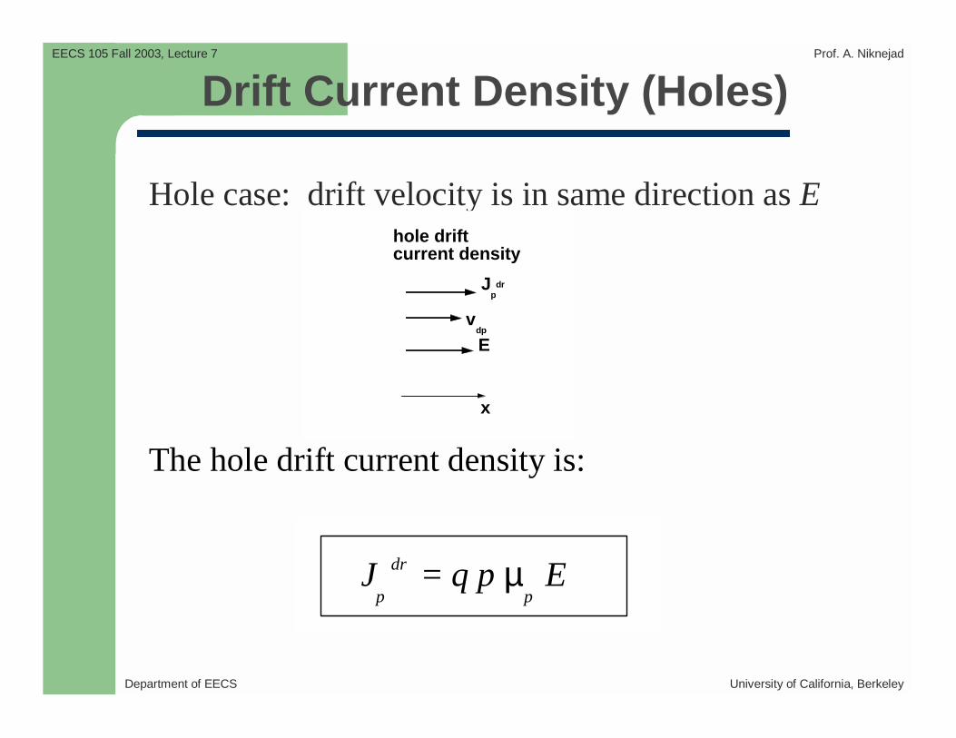
Drift Current Density (Holes)
The hole drift current density is:
Jp
dr
= q p µ
p E
Hole case: drift velocity is in same direction as Ehole driftcurrent density
x
Ev
dp
Jp
dr

Department of EECS University of California, Berkeley
EECS 105 Fall 2003, Lecture 7 Prof. A. Niknejad
Drift Current Density (Electrons)
electron driftcurrent density
x
Ev
dn
Jn
dr
Electron case: drift velocity is in opposite direction as E
The electron drift current density is:
Jndr = (-q) n vdn units: Ccm-2 s-1 = Acm-2
EqnEnqJ nndr
nµµ =−−= )(
( )EqnqpJJJ npdrdr
p nµµ +=+=

Department of EECS University of California, Berkeley
EECS 105 Fall 2003, Lecture 7 Prof. A. Niknejad
Resistivity
Bulk silicon: uniform doping concentration, away from surfaces
n-type example: in equilibrium, no = Nd
When we apply an electric field, n = Nd
ENqnEqJ dnnn µµ ==
Resistivity
Conductivity )(, adneffdnn NNqNq −== µµσ
effdnnn Nq ,
11
µσρ == cm−Ω

Department of EECS University of California, Berkeley
EECS 105 Fall 2003, Lecture 7 Prof. A. Niknejad
IC Fabrication: Si Substrate
Pure Si crystal is starting material (wafer)
The Si wafer is extremely pure (~1 part in a billion impurities)
Why so pure? – Si density is about 5 10^22 atoms/cm^3
– Desire intentional doping from 10^14 – 10^18
– Want unintentional dopants to be about 1-2 orders of magnitude less dense ~ 10^12
Si wafers are polished to about 700 µm thick (mirror finish)
The Si forms the substrate for the IC

Department of EECS University of California, Berkeley
EECS 105 Fall 2003, Lecture 7 Prof. A. Niknejad
IC Fabrication: Oxide
Si has a native oxide: SiO2
SiO2 (Quartz) is extremely stable and very convenient for fabrication
It’s an insulators so it can be used for house interconnection
It can also be used for selective doping
SiO2 windows are etched using photolithography
These openings allow ion implantation into selected regions
SiO2 can block ion implantation in other areas

Department of EECS University of California, Berkeley
EECS 105 Fall 2003, Lecture 7 Prof. A. Niknejad
IC Fabrication: Ion Implantation
Si substrate (p-type)
Grow oxide (thermally)
Add photoresist
Expose (visible or UV source)
Etch (chemical such as HF)
Ion implantation (inject dopants)
Diffuse (increase temperature and allow dopants to diffuse)
P-type Si Substrate
oxide
N-type diffusion region

Department of EECS University of California, Berkeley
EECS 105 Fall 2003, Lecture 7 Prof. A. Niknejad
“Diffusion” Resistor
Using ion implantation/diffusion, the thickness and dopant concentration of resistor is set by process
Shape of the resistor is set by design (layout)
Metal contacts are connected to ends of the resistor
Resistor is capacitively isolation from substrate – Reverse Bias PN Junction!
P-type Si Substrate
N-type Diffusion RegionOxide

Department of EECS University of California, Berkeley
EECS 105 Fall 2003, Lecture 7 Prof. A. Niknejad
Poly Film Resistor
To lower the capacitive parasitics, we should build the resistor further away from substrate
We can deposit a thin film of “poly” Si (heavily doped) material on top of the oxide
The poly will have a certain resistance (say 10 Ohms/sq)
Polysilicon Film (N+ or P+ type) Oxide
P-type Si Substrate

Department of EECS University of California, Berkeley
EECS 105 Fall 2003, Lecture 7 Prof. A. Niknejad
Ohm’s Law
Current I in terms of Jn
Voltage V in terms of electric field
– Result for R
IRV =
JtWJAI ==
LVE /=EWtJtWJAI σ===
VL
WtJtWJAI
σ===
tW
LR
σ1=
tW
LR
ρ=

Department of EECS University of California, Berkeley
EECS 105 Fall 2003, Lecture 7 Prof. A. Niknejad
Sheet Resistance (Rs)
IC resistors have a specified thickness – not under the control of the circuit designer
Eliminate t by absorbing it into a new parameter: the sheet resistance (Rs)
=
==W
LR
W
L
tWt
LR sq
ρρ
“Number of Squares”

Department of EECS University of California, Berkeley
EECS 105 Fall 2003, Lecture 7 Prof. A. Niknejad
Using Sheet Resistance (Rs)
Ion-implanted (or “diffused”) IC resistor

Department of EECS University of California, Berkeley
EECS 105 Fall 2003, Lecture 7 Prof. A. Niknejad
Idealizations
Why does current density Jn “turn”?
What is the thickness of the resistor?
What is the effect of the contact regions?

Department of EECS University of California, Berkeley
EECS 105 Fall 2003, Lecture 7 Prof. A. Niknejad
Diffusion
Diffusion occurs when there exists a concentration gradient
In the figure below, imagine that we fill the left chamber with a gas at temperate T
If we suddenly remove the divider, what happens?
The gas will fill the entire volume of the new chamber. How does this occur?

Department of EECS University of California, Berkeley
EECS 105 Fall 2003, Lecture 7 Prof. A. Niknejad
Diffusion (cont)
The net motion of gas molecules to the right chamber was due to the concentration gradient
If each particle moves on average left or right then eventually half will be in the right chamber
If the molecules were charged (or electrons), then there would be a net current flow
The diffusion current flows from high concentration to low concentration:
Department of EECS University of California, Berkeley
EECS 105 Fall 2003, Lecture 7 Prof. A. Niknejad
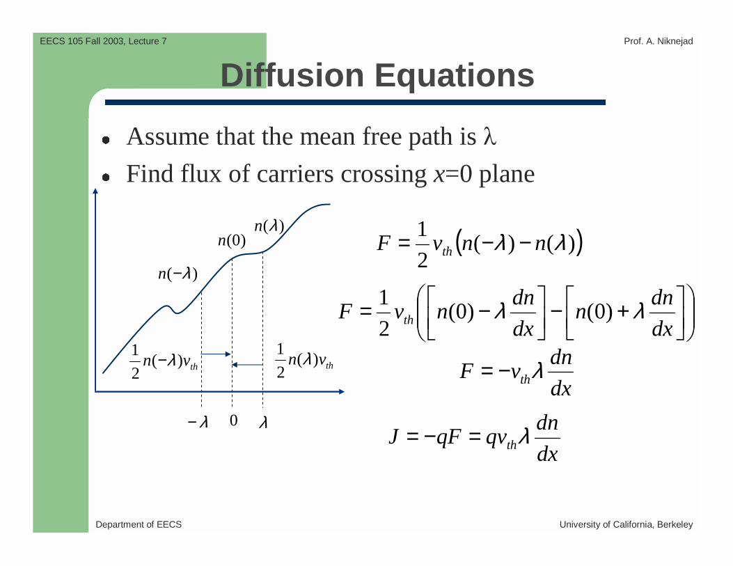
Diffusion Equations
Assume that the mean free path is λ
Find flux of carriers crossing x=0 plane
)(λn)0(n
)( λ−n
0λ− λ
thvn )(2
1 λthvn )(
2
1 λ−
( ))()(2
1 λλ nnvF th −−=
+−
−=dx
dnn
dx
dnnvF th λλ )0()0(
2
1
dx
dnvF thλ−=
dx
dnqvqFJ thλ=−=

Department of EECS University of California, Berkeley
EECS 105 Fall 2003, Lecture 7 Prof. A. Niknejad
Einstein Relation
The thermal velocity is given by kT
kTvm thn 212*
21 =
cthv τλ =Mean Free Time
dx
dn
q
kTq
dx
dnqvJ nth
== µλ
nn q
kTD µ
=
**2
n
c
n
ccthth m
q
q
kT
mkTvv
τττλ ===

Department of EECS University of California, Berkeley
EECS 105 Fall 2003, Lecture 7 Prof. A. Niknejad
Total Current and Boundary Conditions
When both drift and diffusion are present, the total current is given by the sum:
In resistors, the carrier is approximately uniform and the second term is nearly zero
For currents flowing uniformly through an interface (no charge accumulation), the field is discontinous
dx
dnqDnEqJJJ nndiffdrift +=+= µ
21 JJ =
2211 EE σσ =
1
2
2
1
σσ=
E
E
)( 11 σJ
)( 22 σJ

Department of EECS University of California, Berkeley
EECS 105 Fall 2003, Lecture 7 Prof. A. Niknejad
Electrostatics Review (1)
Electric field go from positive charge to negative charge (by convention)
Electric field lines diverge on charge
In words, if the electric field changes magnitude, there has to be charge involved!
Result: In a charge free region, the electric field must be constant!
+++++++++++++++++++++
− − − − − − − − − − − − − − −
ερ=⋅∇ E

Department of EECS University of California, Berkeley
EECS 105 Fall 2003, Lecture 7 Prof. A. Niknejad
Electrostatics Review (2)
Gauss’ Law equivalently says that if there is a netelectric field leaving a region, there has to be positive charge in that region:
+++++++++++++++++++++
− − − − − − − − − − − − − − −
Electric Fields are Leaving This Box!
∫ =⋅εQ
dSE
∫∫ ==⋅∇VV
QdVdVE εερ
/εQ
dSEdVESV∫∫ =⋅=⋅∇
Recall:

Department of EECS University of California, Berkeley
EECS 105 Fall 2003, Lecture 7 Prof. A. Niknejad
Electrostatics in 1D
Everything simplifies in 1-D
Consider a uniform charge distribution
ερ==⋅∇
dx
dEE dxdE
ερ=
')'(
)()(0
0 dxx
xExEx
x∫+=
ερ
)(xρ
xxdx
xxE
x
ερ
ερ 0
0
')'(
)( == ∫
Zero fieldboundarycondition
1x
0ρ
1x
)(xE
10 x
ερ

Department of EECS University of California, Berkeley
EECS 105 Fall 2003, Lecture 7 Prof. A. Niknejad
Electrostatic Potential
The electric field (force) is related to the potential (energy):
Negative sign says that field lines go from high potential points to lower potential points (negative slope)
Note: An electron should “float” to a high potential point:
dx
dE
φ−=
dx
deqEFe
φ−==1φ
2φ
dx
deFe
φ−=e

Department of EECS University of California, Berkeley
EECS 105 Fall 2003, Lecture 7 Prof. A. Niknejad
More Potential
Integrating this basic relation, we have that the potential is the integral of the field:
In 1D, this is a simple integral:
Going the other way, we have Poisson’s equation in 1D:
∫ ⋅−=−C
ldExxr
)()( 0φφ
)(xφ
)( 0xφ E
ldr
∫−=−x
xdxxExx
0
')'()()( 0φφ
ερφ )()(
2
2 x
dx
xd −=

Department of EECS University of California, Berkeley
EECS 105 Fall 2003, Lecture 7 Prof. A. Niknejad
Boundary Conditions
Potential must be a continuous function. If not, the fields (forces) would be infinite
Electric fields need not be continuous. We have already seen that the electric fields diverge on charges. In fact, across an interface we have:
Field discontiuity implies charge density at surface!
)( 11 εE
)( 22 εE
∫ =+−=⋅ insideQSESEdSE 2211 εεεx∆
00
→ →∆xinsideQ
02211 =+− SESE εε
1
2
2
1
εε=
E
ES
Department of EECS University of California, Berkeley
EECS 105 Fall 2003, Lecture 7 Prof. A. Niknejad
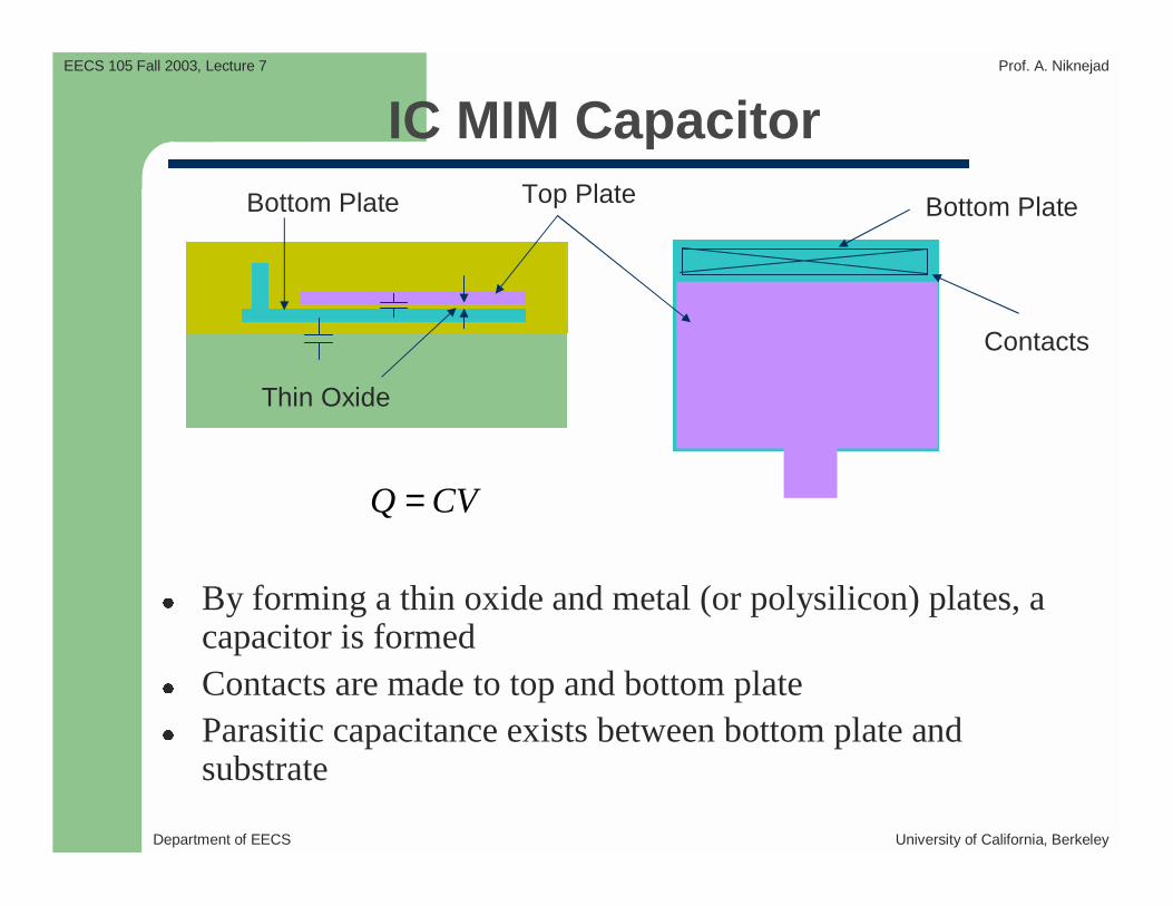
IC MIM Capacitor
By forming a thin oxide and metal (or polysilicon) plates, a capacitor is formed
Contacts are made to top and bottom plate Parasitic capacitance exists between bottom plate and
substrate
Top PlateBottom Plate Bottom Plate
Contacts
CVQ =
Thin Oxide

Department of EECS University of California, Berkeley
EECS 105 Fall 2003, Lecture 7 Prof. A. Niknejad
Review of Capacitors
For an ideal metal, all charge must be at surface
Gauss’ law: Surface integral of electric field over closed surface equals charge inside volume
+++++++++++++++++++++
− − − − − − − − − − − − − − −
+−
Vs
∫ =⋅εQ
dSE
∫ −=⋅εQ
dSE
sox VtEdlE ==⋅∫ 0ox
s
t
VE =0
∫ ==⋅εQ
AEdSE 0 εQ
At
V
ox
s =
sCVQ =
oxt
AC
ε=

Department of EECS University of California, Berkeley
EECS 105 Fall 2003, Lecture 7 Prof. A. Niknejad
Capacitor Q-V Relation
Total charge is linearly related to voltage
Charge density is a delta function at surface (for perfect metals)
sCVQ =
sV
Q
y
)(yQ
y+++++++++++++++++++++
− − − − − − − − − − − − − − −

Department of EECS University of California, Berkeley
EECS 105 Fall 2003, Lecture 7 Prof. A. Niknejad
A Non-Linear Capacitor
We’ll soon meet capacitors that have a non-linear Q-V relationship
If plates are not ideal metal, the charge density can penetrate into surface
)( sVfQ =
sV
Q
y
)(yQ
y+++++++++++++++++++++
− − − − − − − − − − − − − − −

Department of EECS University of California, Berkeley
EECS 105 Fall 2003, Lecture 7 Prof. A. Niknejad
What’s the Capacitance?
For a non-linear capacitor, we have
We can’t identify a capacitance
Imagine we apply a small signal on top of a bias voltage:
The incremental charge is therefore:
ss CVVfQ ≠= )(
sVV
sss vdV
VdfVfvVfQ
s=
+≈+= )()()(
Constant charge
sVV
s vdV
VdfVfqQQ
s=
+≈+= )()(0

Department of EECS University of California, Berkeley
EECS 105 Fall 2003, Lecture 7 Prof. A. Niknejad
Small Signal Capacitance
Break the equation for total charge into two terms:
sVV
s vdV
VdfVfqQQ
s=
+≈+= )()(0
ConstantCharge
IncrementalCharge
ssVV
vCvdV
Vdfq
s
===
)(
sVVdV
VdfC
=
≡ )(
Department of EECS University of California, Berkeley
EECS 105 Fall 2003, Lecture 7 Prof. A. Niknejad
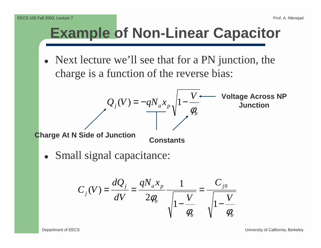
Example of Non-Linear Capacitor
Next lecture we’ll see that for a PN junction, the charge is a function of the reverse bias:
Small signal capacitance:
bpaj
VxqNVQ
φ−−= 1)(
ConstantsCharge At N Side of Junction
Voltage Across NPJunction
b
j
b
b
pajj
V
C
V
xqN
dV
dQVC
φφφ
−=
−==
11
1
2)( 0
Recommended