Eclipse Series
RF Technology [email protected]
February, 2003
PA 150 Amplifier Operation and Maintenance Manual
This manual is produced by RF Technology Pty Ltd
10/8 Leighton Place, Hornsby NSW 2077 Australia. Copyright © 1997 RF Technology.
RF Technology PA150 Page 2
CONTENTS CONTENTS Contents 1 Operating Instructions 3 1 1.1 Front Panel Indicators 3
1.2 Internal Adjustments 3 1.3 Output Power 3 1.4 RF Level Detector 3
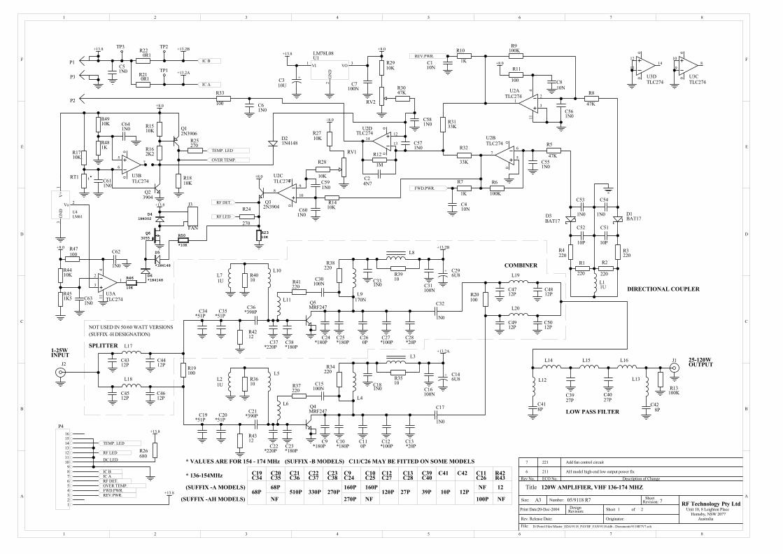
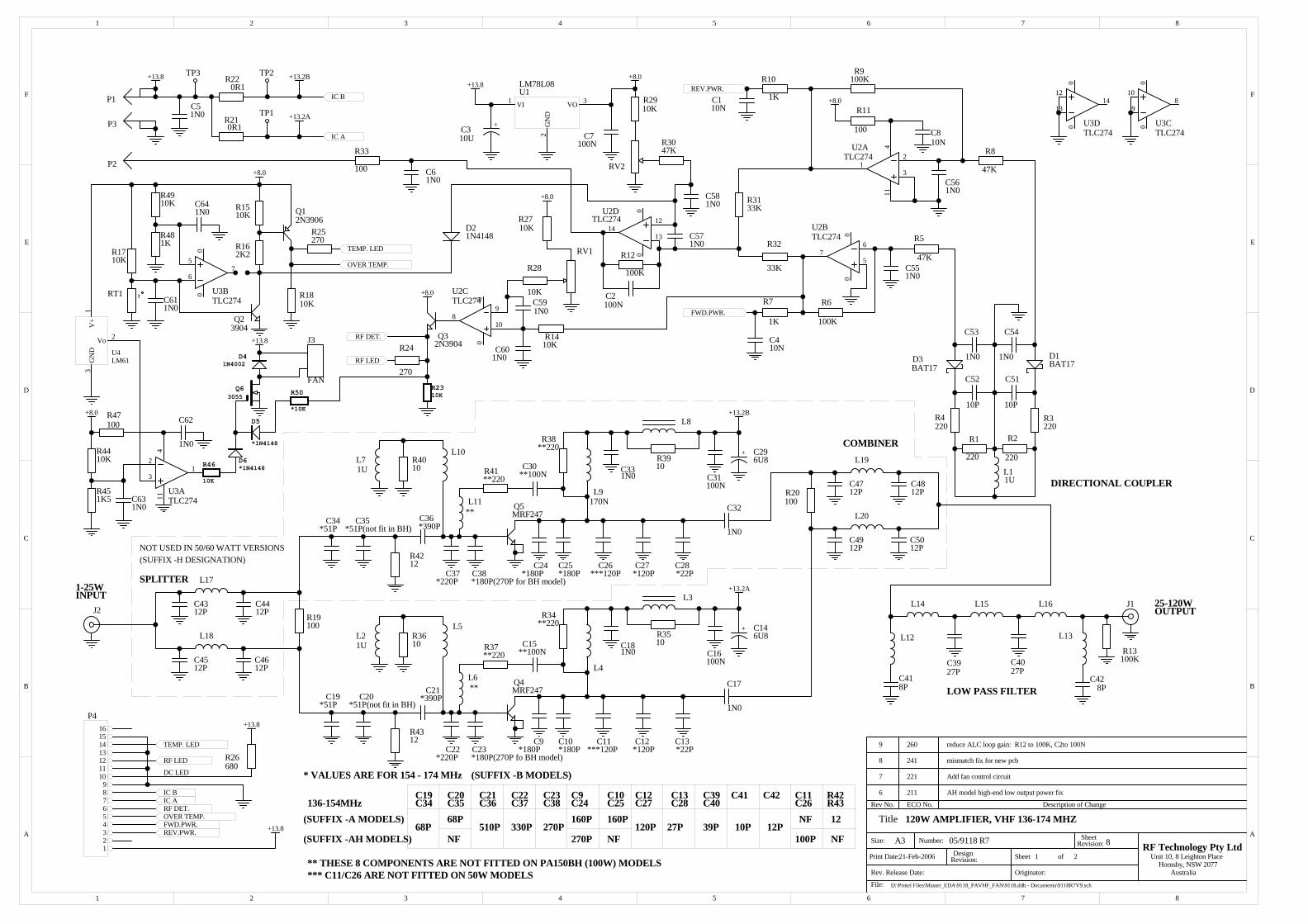
2 Circuit Description 4
2.1 Amplifiers 4 2.2 Power Splitter/Combiners 5 2.3 Directional Coupler 5 2.4 Low pass Filter 5 2.5 Power Control Circuits 5 2.6 RF Output Indicator 5 2.7 Over Temperature Protection 6
3 Alignment Procedure 6 4 Specifications 7
4.1 Description 7 4.2 Physical Configuration 7 4.3 Front Indicators and Test Points 7
4.3.1 Indicators 7 4.3.2 Test Points 8
5 Electrical Specifications 8
5.1 Power Requirements 8 5.2 Frequency Range 8 5.3 Nominal Antenna Impedance 8 5.4 Output Power 8 5.5 Transmit Duty Cycle 8 5.6 Spurious and Harmonics 8 5.7 Maximum Heatsink Temperature 9 5.8 ALC Output 9 5.9 Mis-Match Protection 9
6 Conectors 9 6.1 Antenna Connector 9
6.2 Power and I/O Connector 9 6.3 Test Connector 9
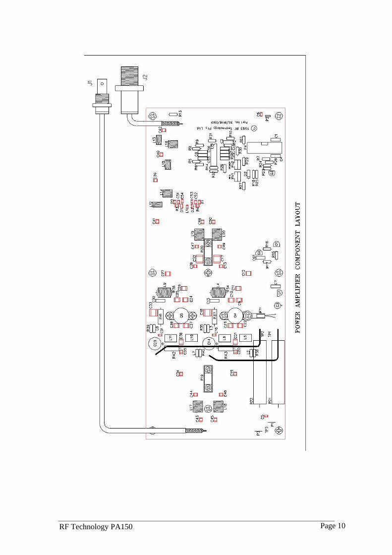
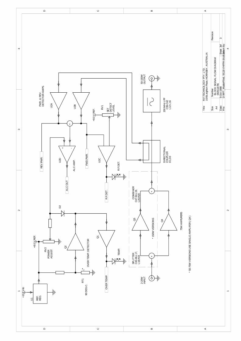
7 Appendix A Block Diagram 10 Schematic Diagram Board Layout 11 Parts List 12
RF Technology PA150 Page 3
1 OPERATING INSTRUCTIONS 1 Operating Instructions 1.1 Front Panel Indicators
PWR LED The Power LED shows that the dc supply is connected to the transmitter.
RFO LED
The RF Output LED indicates that the amplifier is being driven and that the forward output power is above a preset level. The indication level is set by RV1 which is accessible through the side of the case. (After removing 20 screws)
TEMP LED
The Temperature LED indicates when the amplifier temperature is too high. The power is automatically reduced if the output transistors temperature rises above safe limits.
1.2 Internal Adjustments
All internal adjustments are factory set and should not need readjustment under normal conditions.
1.3 Output Power
The output power is set to the desired level watts by RV2. It determines the threshold of the ALC voltage which is fed back to the transmitter module to regulate the power. The output power of standard amplifiers can be set to any level between 25 and 75 watts. The high power versions with “H” suffix model numbers can be set between 50 and 100 watts.
WARNING
Changes or modifications not expressly approved by RF Technology could void your authority to operate this equipment. Specifications may vary from those
given in this document in accordance with requirements of local authorities. RF Technology
equipment is subject to continual improvement and RF Technology reserve the right to change performance and
specification without further notice.
RF Technology PA150 Page 4
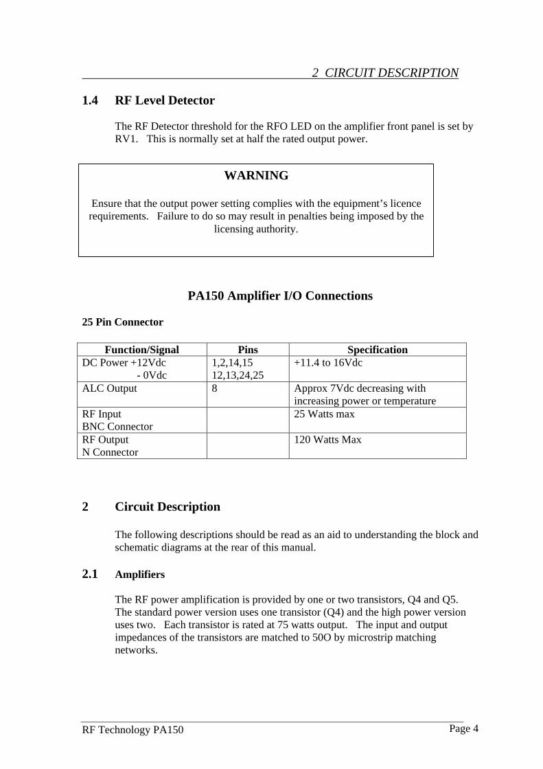
2 CIRCUIT DESCRIPTION 1.4 RF Level Detector
The RF Detector threshold for the RFO LED on the amplifier front panel is set by RV1. This is normally set at half the rated output power.
PA150 Amplifier I/O Connections 25 Pin Connector
Function/Signal Pins Specification
DC Power +12Vdc - 0Vdc
1,2,14,15 12,13,24,25
+11.4 to 16Vdc
ALC Output 8 Approx 7Vdc decreasing with increasing power or temperature
RF Input BNC Connector
25 Watts max
RF Output N Connector
120 Watts Max
2 Circuit Description
The following descriptions should be read as an aid to understanding the block and schematic diagrams at the rear of this manual.
2.1 Amplifiers
The RF power amplification is provided by one or two transistors, Q4 and Q5. The standard power version uses one transistor (Q4) and the high power version uses two. Each transistor is rated at 75 watts output. The input and output impedances of the transistors are matched to 50O by microstrip matching networks.
WARNING
Ensure that the output power setting complies with the equipment’s licence requirements. Failure to do so may result in penalties being imposed by the
licensing authority.
RF Technology PA150 Page 5
2 CIRCUIT DESCRIPTION
The amplifiers are broad band and do not have any tuning adjustments. The “A” versions are optimized for the frequency range 136-156 MHz while the “B” versions cover 154-174 MHz. The dc supply is fed to the amplifiers through resistors R21 and R22. This allows the collector current of each amplifier to be measured at the test socket.
2.2 Power Splitter/Combiners
The high power versions use zero degree power splitters and combiners. They consist of lumped element 1/4 wave 70O pi networks and 100O RF resistors (C43-50, L17-20, R19-20). This configuration provides wider bandwidth and better balance than lower cost 90 degree hybrids.
2.3 Directional Coupler
The forward and reverse power components are measured throug a coupled line directional coupler. The output of the coupled line is frequency compensated by R1-4 and C51-52 before being detected by D1 and D3. The voltage output of the detectors is proportional to the forward and reflected power.
2.4 Low Pass Filter
A low pass filter consisting of L12-16 and C39-42 reduces the harmonic components to less than -80dBc. The filter uses a combination of lumped elements and printed microstrips to obtain the required harmonic attenuation.
2.5 Power Control Circuits
The forward and reverse voltages from the directional coupler are amplified and inverted by U2a and U2b. The amplified voltages are combined before connecting to the input of error amplifier U2d. Error amplifier U2d compares the detected voltage with the dc reference voltage from output power trimpot RV2. The amplified difference at the output U2d is supplied to the rear panel system connector for connection to the T150 ALC input.
2.6 RF Output Indicator
The forward power voltage is compared with the pre-set dc reference voltage from RV1 and U2c. The output of U2c is used to turn on the RFO LED and provide an output power logic signal to the test connector.
RF Technology PA150 Page 6
3 ALIGNMENT PROCEDURE RV1 is normally set so that the RFO LED comes ON at 1-3 db below the normal power output.
2.7 Over Temperature Protection
Thermistor RT1 is mounted to the case of output transistor Q4. If the transistor case temperature rises above 90 degrees C the resistance of RT1 increases and Q2 is turned ON.
This causes the TEMP LED to come on and also reduces the dc reference voltage to the output power error amplifier U2d. The input power will then be reduced by the transmitter ALC circuits and the output transistors are kept within safe operating limits.
3 Alignment Procedure
The following procedures may be used to align the amplifier for optimum performance.
Standard Test Conditions
RF Input Source Power Supply Load T150 Series transmitter 25 watts maximum
13.8 Vdc at 15 A 50O 150 watts VSWR < 1.2:1
Set RFO Level
Step Input Measure Adjust 1 None Set RV1 and R2 Fully counter
clockwise 2 Centre channel
frequency from the T150, 25W max threshold
RF output power at J2
Key transmitter adjust RV2 for desired output
3 As above RFO LED Key transmitter adjust RV1 to where the RFO LED just goes OFF
RF Technology PA150 Page 7
4 SPECIFICATIONS Set Output Power
Step Input Measure Adjust 4 As above RF output power at
J2 Key transmitter. Adjust RV2 for the desired power
4 Specifications 4.1 Description
The power amplifiers are designed for use with the T150 series transmitters to provide 50-150 watts output. Output power regulation is provided by connecting the output of the directional coupler to the ALC input of the T150. the drive from the transmitter is then automatically adjusted to maintain the required output. The regulated power level can be preset over a wide range from 25 to 150 watts depending on the available driver power. Sensing circuits are provided to protect the output transistors from excessive temperatures. If the output transistor case temperature rises to 90 degrees C, the input drive will be reduced to prevent damage.
4.2 Physical Configuration
The power amplifier is designed to fit in a 19 inch rack mounted frame. The installed height is 4RU (178mm) and the depth is 350mm. The amplifier is 95.25mm or three Elcipse modules wide. An extruded aluminium heat sink with vertical fins is used. The temperature rise is normally less than 30 degrees at 50 watts output.
4.3 Front Indicators and Test Points 4.3.1 Indicators
Power ON - Green LED RF Power Output - Yellow LED Over Temperature - Red LED
RF Technology PA150 Page 8
5 ELECTRICAL SPECIFICATIONS
4.3.2 Test Points (DB9 Connector)
Forward Power Pin 8 + Gnd (pin 1) Reverse Power Pin 4 + Gnd (pin 1) Collector Current Pin 6, Pin 2 + Vcc 13.2Vdc
5 Electrical Specifications
5.1 Power Requirements
Operating Voltage - 10.5 to 16 Vdc with output power reduced below 12.5 Vdc. Current Drain @ 13.2 Vdc - 10 Amps Max at 50 watts. 100 mA Max standby Polarity - Negative Ground
5.2 Frequency Range
Frequency 50 Watt 100 Watt 136-156MHz PA150A PA150AH 154-174 MHz PA150B PA150BH
5.3 Nominal Antenna Impedance
50O
5.4 Output Power
25 to 100 watts adjustable 5.5 Transmit Duty Cycle
With Free Air Circulation 50 Watts - 100% to 40 deg. C 100 Watts - 50% to 40 deg. C With Fan Module 50-100 Watts - 100% to 50 deg. C
5.6 Spurious and Harmonics Less than 0.25uW
RF Technology PA150 Page 9
Connectors
5.7 Maximum Heatsink Temperature 90 degrees C.
5.8 ALC Output
The ALC is intended for connection to the T150. It supplies a voltage which decreases with increasing power or temperature.
5.9 Mis-Match Protection
The amplifier is protected from damage when operating into a VSWR of 10/1 at all phase angles.
6 Connectors
6.1 Antenna Connector
Type N Female mounted on the module rear panel 6.2 Power and I/O Connector
25 pin “D” Male mounted on the rear panel 6.3 Test Connector
9 pin “D” Female mounted on the front panel.
RF Technology PA150 Page 10
12
34
ABCD
43
21
D C B ATi
tle
Num
ber
Rev
isio
nSi
ze A4
Dat
e:9-
Oct
-199
8Sh
eet
ofFi
le:
D:\R
FT_M
aste
rFile
s\..\
9118
-VH
FPA
-blo
ck.s
chDra
wn
By:
-+
+
+8.0
V.R
EF.
POW
ERA
DJU
ST
OU
TPU
T
200
MH
zLP
FD
IREC
TIO
NA
LC
OU
PLER
FWD
.PW
R.
REV
.PW
R.
U2D
ALC
OU
T
+13.
8V
dc
U1
++
INPU
T
+8.0
V.R
EF.
U2C
C39
-C42
L12-
L16
SPLI
TTER
CO
MB
INER
D1,
D3
75W
AM
PLIF
IERS
SET
DET
ECT
LEV
EL
R.F
.DET
.
REF
.R
EG.
OV
ERTE
MP.
DET
ECTO
R
OV
ERTE
MP.
ALC
AM
P.
FWD
.&R
EV.
DET
ECTO
RA
MPS
.
C47
-50,
L19,
L20,
R20
2-20
W
C43
-46,
L17,
L18,
R19
*15
0WV
ERSI
ON
S
*50
-75W
VER
SIO
NS
USE
SIN
GLE
AM
PLIF
ER(Q
4)
50-1
50W
TEM
P.R
.F.D
ET.
tR
T190
DEG
.C.
D2
U2BU2A
RV
1
RV
2 Q2
Q1
Q5
Q4
R.F
.TEC
HN
OLO
GY
PTY
.LTD
.10
/8Le
ight
onPl
ace,
HO
RN
SBY
,AU
STR
ALI
A
BLO
CK
SIG
NA
LFL
OW
DIA
GR
AM
05/9
118
R6
33

12
34
ABCD
43
21
D C B ATi
tle
Num
ber
Rev
ision
Size Orc
adA
Dat
e:3-
Aug
-199
8Sh
eet
ofFi
le:
D:\R
FT_M
aste
rFile
s\..\
9118
-blo
ck.s
chD
raw
nB
y:
AM
PLIF
IER
PCB
ASS
Y11
/911
8
+13.
8
A.L
.C.
0V
PWR
AL
CT
EM
P
LE
DPC
BA
SSY
11/9
106
+13.
8
REV
.PW
R.
FWD
.PW
R.
OV
ERTE
MP.
IcB
IcA
0V RF.
DET
.
INPU
T
OU
TPU
T
13251224112310229218207196185174163152141P5 C
ON
NE
CT
OR
DB
25
J3J1P1
J2P2 P3
12345678910111213141516
P4
12345678910111213141516J5
594837261J6 C
ON
NE
CT
OR
DB
9
D1
D2
D3
+-
+-
+-
J1 BN
C
J2 NTy
pe
R41
100
RF
TE
CH
NO
LO
GY
PTY
.LT
D.
10/8
Lei
ghto
nPL
ace,
HO
RN
SBY
,207
7,A
ustr
alia
9118
(VH
FA
MPL
IFIE
R)
3
33
JBS
afte
rR
HM
RF Technology PA150 Page 11
B PA150 PARTS LIST Ref. Description Part Number NOTE - ALL COMPONENTS FOR WHICH REF IS ACCOMPANIED WITH AN ASTERIX (*) ARE USED ONLY IN HIGH POWER MODELS (PA150XH) C1 CAP 10N 10% 50V X7R RAD.2 46/2001/010N C2 CAP 4N7 5% 400V MKT RAD.2 47/2040/04N7 C3 CAP 10U 35V RAD ELECTRO 41/2001/010U C4 CAP 10N 10% 50V X7R RAD.2 46/2001/010N C5 CAP 1N0 5% 63V NPO SM1206 46/3300/01N0 C6 CAP 1N0 5% 63V NPO SM1206 46/3300/01N0 C7 CAP 100N 10% 50V X7R RAD.2 46/2001/100N C8 CAP 10N 10% 50V X7R RAD.2 46/2001/010N C14 CAP 6.8U 20% 25V SOLID AL 41/2225/06U8 C15 CAP 100N 10% 50V X7R RAD.2 46/2001/100N C16 CAP 100N 10% 63V X7R 1206 46/3310/100N C17 CAP 1N0 500V MICA SM2220 48/3003/01N0 C18 CAP 1N0 500V MICA SM2220 48/3003/01N0 C29* CAP 6.8U 20% 25V SOLID AL 41/2225/06U8 C30* CAP 100N 10% 50V X7R RAD.2 46/2001/100N C31* CAP 100N 10% 63V X7R 1206 46/3310/100N C32* CAP 1N0 500V MICA SM2220 48/3003/01N0 C33* CAP 1N0 500V MICA SM2220 48/3003/01N0 C43* CAP 12P 500V MICA SM1210 48/3003/012P C44* CAP 12P 500V MICA SM1210 48/3003/012P C45* CAP 12P 500V MICA SM1210 48/3003/012P C46* CAP 12P 500V MICA SM1210 48/3003/012P C47* CAP 12P 500V MICA SM1210 48/3003/012P C48* CAP 12P 500V MICA SM1210 48/3003/012P C49* CAP 12P 500V MICA SM1210 48/3003/012P C50* CAP 12P 500V MICA SM1210 48/3003/012P C51 CAP 10P 5% 63V NPO SM 1206 46/3300/010P C52 CAP 10P 5% 63V NPO SM1206 46/3300/010P C53 CAP 1N0 5% 63V NPO SM1206 46/3300/01N0 C54 CAP 1N0 5% 63V NPO SM1206 46/3300/01N0 C55 CAP 1N0 5% 100V NPO RAD.2 46/2000/01N0 C56 CAP 1N0 5% 100V NPO RAD.2 46/2000/01N0 C57 CAP 1N0 5% 100V NPO RAD.2 46/2000/01N0 C58 CAP 1N0 5% 100V NPO RAD.2 46/2000/01N0 C59 CAP 1N0 5% 100V NPO RAD.2 46/2000/01N0 C60 CAP 1N0 5% 100V NPO RAD.2 46/2000/01N0 C61 CAP 1N0 5% 100V NPO RAD.2 46/2000/01N0 D1 DIODE SHTKY BAT17 SOT23 21/3030/0017 D2 DIODE SILICON 1N4148 21/1010/4148 D3 DIODE SHTKY BAT17 SOT23 21/3030/0017 L1 IND 1U0 10% CHOKE SM1206 37/3320/01U0 L2 INDUCTOR 1UH AXIAL 37/2021/001U L3 FERRITE BEAD 3x4x1 4S2 37/1022/0001 L4 COIL AIR COR 7T 1.5P 6.35ID 37/1635/1507 L5 IND MOLDED 6.5 TURN 37/2021/0006 L6 IND MOLDED 6.5 TURN 37/2021/0006 L7* INDUCTOR 1UH AXIAL 37/2021/001U L8* FERRITE BEAD 3x4x14S2 37/1022/0001
RF Technology PA150 Page 12
B PA150 PARTS LIST Ref. Description Part Number L9* COIL AIR CORE 7T 1.5P 6.35ID 37/1635/1507 L10* IND MOLDED 6.5 TURN 37/2021/0006 L11* IND MOLDED 6.5 TURN 37/2021/0006 L12 COIL AIR CORE 2T 2P 6.35ID 37/1400/1002 L13 COIL AIR CORE 2T 2P 6.35ID 37/1400/1002 L14 COIL AIR CORE 3T 2P 6.35ID 37/1635/2003 L15 COIL AIR CORE 3T 5P 6.35ID 37/1635/1503 L16 COIL AIR CORE 3T 2P 6.35ID 37/1635/2003 L17 INDUCTOR, MOULDED 7.5T 37/2021/0007 L18 INDUCTOR, MOULDED 7.5T 37/2021/0007 L19* COIL AIR CORE 6T 1.5P 4D 37/1400/1006 L20* COIL AIR CORE 6T 1.5P 4D 37/1400/1006 P1 6.35mm QC TAB VERT PCB MT 35/0635/0001 P3 6.35mm QC TAB VERT PCB MT 35/0635/0001 P4 CON 16WAY SHR'D HEADER 35/2502/0016 Q1 TRSTR GP PNP 2N3906 TO92 27/2010/3906 Q2 TRSTR GP NPN 2N3904 TO92 27/2020/3904 Q3 TRSTR GP NPN 2N3904 TO92 27/2020/3904 Q4 TRSTR NPN VHF RF MRF247 27/3020/MRF247 Q5* TRSTR NPN VHF RF MRF247 27/3020/MRF247 R1 RES 220 5% 0.25W SM1206 51/3380/0220 R2 RES 220 5% 0.25W SM1206 51/3380/0220 R3 RES 220 5% 0.25W SM1206 51/3380/0220 R4 RES 220 5% 0.25W SM1206 51/3380/0220 R5 RES 47K 5% 0.25W AXIAL 51/1040/047K R6 RES 100K 5% 0.25W AXIAL 51/1040/100K R7 RES 1K0 5% 0.25W AXIAL 51/1040/01K0 R8 RES 47K 5% 0.25W AXIAL 51/1040/047K R9 RES 100K 5% 0.25W AXIAL 51/1040/100K R10 RES 1K0 5% 0.25W AXIAL 51/1040/01K0 R11 RES 100 5% 0.25W AXIAL 51/1040/0100 R12 RES 1M0 5% 0.25W AXIAL 51/1040/01M0 R13 RES 100K 5% 0.25W AXIAL 51/1040/100K R14 RES 10K 5% 0.25W AXIAL 51/1040/010K R15 RES 10K 5% 0.25W AXIAL 51/1040/010K R16 RES 2K2 5% 0.25W AXIAL 51/1040/2K2 R17 RES 10K 5% 0.25W AXIAL 51/1040/010K R18 RES 10K 5% 0.25W AXIAL 51/1040/101K R19* RES 100 OHM 40W RF 51/RF40/0100 R20* RES 100 OHM 40W RF 51/RF40/0100 R21 RES 0.1 5% 10W ASW 10 51/0010/00R1 R22* RES 0.1 5% 10W ASW 10 51/0010/00R1 R23 RES 10K 5% 0.25W AXIAL 51/1040/010K R24 RES 270 5% 0.25W AXIAL 51/1040/0270 R25 RES 270 5% 0.25W AXIAL 51/1040/0270 R26 RES 680 5% 0.25W AXIAL 51/1040/0680 R27 RES 10K 5% 0.25W AXIAL 51/1040/010K R28 RES 10K 5% 0.25W AXIAL 51/1040/010K R29 RES 10K 5% 0.25W AXIAL 51/1040/010K R30 RES 47K 5% 0.25W AXIAL 51/1040/047K R31 RES 33K 5% 0.25W AXIAL 51/1040/033K
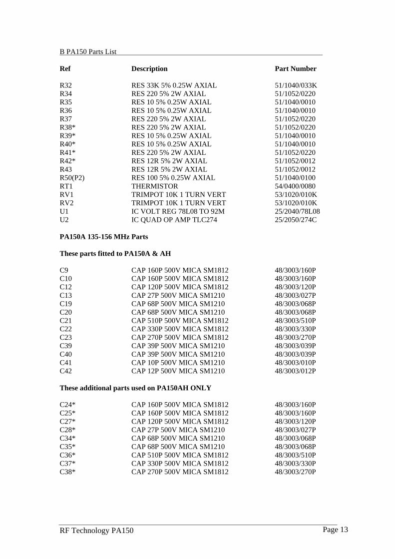
RF Technology PA150 Page 13
B PA150 Parts List Ref Description Part Number R32 RES 33K 5% 0.25W AXIAL 51/1040/033K R34 RES 220 5% 2W AXIAL 51/1052/0220 R35 RES 10 5% 0.25W AXIAL 51/1040/0010 R36 RES 10 5% 0.25W AXIAL 51/1040/0010 R37 RES 220 5% 2W AXIAL 51/1052/0220 R38* RES 220 5% 2W AXIAL 51/1052/0220 R39* RES 10 5% 0.25W AXIAL 51/1040/0010 R40* RES 10 5% 0.25W AXIAL 51/1040/0010 R41* RES 220 5% 2W AXIAL 51/1052/0220 R42* RES 12R 5% 2W AXIAL 51/1052/0012 R43 RES 12R 5% 2W AXIAL 51/1052/0012 R50(P2) RES 100 5% 0.25W AXIAL 51/1040/0100 RT1 THERMISTOR 54/0400/0080 RV1 TRIMPOT 10K 1 TURN VERT 53/1020/010K RV2 TRIMPOT 10K 1 TURN VERT 53/1020/010K U1 IC VOLT REG 78L08 TO 92M 25/2040/78L08 U2 IC QUAD OP AMP TLC274 25/2050/274C PA150A 135-156 MHz Parts These parts fitted to PA150A & AH C9 CAP 160P 500V MICA SM1812 48/3003/160P C10 CAP 160P 500V MICA SM1812 48/3003/160P C12 CAP 120P 500V MICA SM1812 48/3003/120P C13 CAP 27P 500V MICA SM1210 48/3003/027P C19 CAP 68P 500V MICA SM1210 48/3003/068P C20 CAP 68P 500V MICA SM1210 48/3003/068P C21 CAP 510P 500V MICA SM1812 48/3003/510P C22 CAP 330P 500V MICA SM1812 48/3003/330P C23 CAP 270P 500V MICA SM1812 48/3003/270P C39 CAP 39P 500V MICA SM1210 48/3003/039P C40 CAP 39P 500V MICA SM1210 48/3003/039P C41 CAP 10P 500V MICA SM1210 48/3003/010P C42 CAP 12P 500V MICA SM1210 48/3003/012P These additional parts used on PA150AH ONLY C24* CAP 160P 500V MICA SM1812 48/3003/160P C25* CAP 160P 500V MICA SM1812 48/3003/160P C27* CAP 120P 500V MICA SM1812 48/3003/120P C28* CAP 27P 500V MICA SM1210 48/3003/027P C34* CAP 68P 500V MICA SM1210 48/3003/068P C35* CAP 68P 500V MICA SM1210 48/3003/068P C36* CAP 510P 500V MICA SM1812 48/3003/510P C37* CAP 330P 500V MICA SM1812 48/3003/330P C38* CAP 270P 500V MICA SM1812 48/3003/270P

RF Technology PA150 Page 14
B PA150 Parts List Ref Description Part Number PA150B 154-174 MHz Parts These parts fitted to PA150B & BH C9 CAP 180P 500V MICA SM1812 48/3003/180P C10 CAP 180P 500V MICA SM1812 48/3003/180P C12 CAP 100P 500V MICA SM1812 48/3003/100P C13 CAP 20P 500V MICA SM1210 48/3003/020P C19 CAP 51P 500V MICA SM1210 48/3003/051P C20 CAP 51P 500V MICA SM1210 48/3003/051P C21 CAP 390P 500V MICA SM1812 48/3003/390P C22 CAP 220P 500V MICA SM1812 48/3003/220P C23 CAP 180P 500V MICA SM1812 48/3003/180P C39 CAP 27P 500V MICA SM1210 48/3003/027P C40 CAP 27P 500V MICA SM1210 48/3003/027P C41 CAP 8P 500V MICA SM1210 48/3003/008P C42 CAP 8P 500V MICA SM1210 48/3003/008P These additional parts used on PA150BH ONLY C11 CAP 160P 500V MICA SM1812 48/3003/160P C24* CAP 180P 500V MICA SM1812 48/3003/180P C25* CAP 180P 500V MICA SM1812 48/3003/180P C26 CAP 160P 500V MICA SM1812 48/3003/160P C27* CAP 100P 500V MICA SM1812 48/3003/100P C28* CAP 20P 500V MICA SM1210 48/3003/020P C34* CAP 51P 500V MICA SM1210 48/3003/051P C35* CAP 51P 500V MCA SM1210 48/3003/051P C36* CAP 390P 500V MICA SM1812 48/3003/390P C37* CAP 220P 500V MICA SM1812 48/3003/220P C38* CAP 180P 500V MICA SM1812 48/3003/180P End parts list
1 2 3 4 5 6 7 8
A
B
C
D
E
F
87654321
F
E
D
C
B
A
1 2
120W AMPLIFIER, VHF 136-174 MHZ
05/9118 R7 720-Dec-2004
D:\Protel Files\Master_EDA\9118_PAVHF_FAN\9118.ddb - Documents\9118R7V7.sch
Title
Size: Number:
Print Date:
File:
Revision:
Sheet of
A3RF Technology Pty Ltd
Unit 10, 8 Leighton PlaceHornsby, NSW 2077
AustraliaRev. Release Date: Originator:
Rev No. ECO No. Description of Change
Sheet
Revision:Design
LOW PASS FILTER
COMBINER
DIRECTIONAL COUPLER
SPLITTER
FWD.PWR.
REV.PWR.
IC A
FWD.PWR.REV.PWR.
IC BIC ARF DET.OVER TEMP.
RF DET.
RF LED
RF LED
TEMP. LED
TEMP. LED
IC B
OVER TEMP.
DC LED
+8.0
+8.0+13.8 +13.2B
+13.2A
+13.8
+8.0
+8.0
+8.0
+13.8
+13.8
+13.2A
+13.2B
NOT USED IN 50/60 WATT VERSIONS
1-25WINPUT
25-120WOUTPUT
L11U
R1
220
R2
220
R3220
R4220
D1BAT17
R6
100K
R7
1K
R9100KR10
1KR11
100
C110N
R12
1M
C24N7
R13100K
J1
TP1
TP2
+C310U
VI1
GN
D2
VO 3U1LM78L08
R1410K
tRT1
D21N4148
Q12N3906
Q23904
R1510K
R162K2R17
10K
R1810K
C410N
C51N0
C61N0
C7100N
J2
Q32N3904
R19100
R20100
R210R1
R220R1
TP3
C810N
P1
P2
P3
123456789
10111213141516
P4
R24
270
R25270
R26680
R2710K
RV1
R28
10K
RV2
R2910K
R3047K
D3BAT17
R3133K
R32
33K
12
1314
00
U2DTLC274
+ C146U8
C16100N
C17
1N0
R34220
C181N0
R3510
C19*51P
C20*51P
C22*220P
C23*180P
Q4MRF247
R37220
L6
+ C296U8
C31100N
C32
1N0
R38220
C331N0
R3910
C34*51P
C35*51P
C37*220P
C38*180P
Q5MRF247
R41220
L11
C3927P
C4027P
C418P
C428P
C4312P
C4412P
C4512P
C4612P
C4712P
C4812P
C4912P
C5012P
C53
1N0
C54
1N0
C551N0
C561N0
C571N0
C581N0
C591N0
C601N0
C611N0
L10
L15
L12 L13
L14 L16
L9170N
L17
L18
L19
L20
C52
10P
C51
10P
L5
L3
L8
R3610
L21U
C21*390P
L4
C15100N
C110P
C260P
C36*390P
L71U
R4010 C30
100N
R4212
R4312
R8
47K
R5
47K
C9*180P
C10*180P
C24*180P
C25*180P
C12*100P
C13*20P
C27*100P
C28*20P
(SUFFIX -H DESIGNATION)
3
21
114U2A
TLC274
5
67
00
U2BTLC274
10
98
00
U2CTLC274
5
67
00 U3B
TLC274
3
21
114
U3ATLC274
R481K
R4910K
R4410K
R451K5
R47100
+8.0
C631N0
J3
FAN
+13.8
C62
1N0
R33
100
C641N0
12
1314
00 U3D
TLC274
10
98
00 U3C
TLC274
Q63055 R50
*10K
D6*1N4148
D5
*1N4148
R4610K
D41N4002
R2310K
V+
1
Vo 2
GN
D3
U4LM61
6
221 Add fan control circuit* VALUES ARE FOR 154 - 174 MHz
C19 C20 C21 C22 C23C34 C35 C36 C37 C38
C9C24
C10C25
160P 160P
C12C27
120P
C13C28
27P68P
* 136-154MHz
68P510P 330P 270P
C39C40
C41 C42
10P 12P39P(SUFFIX -A MODELS)
(SUFFIX -B MODELS) C11/C26 MAY BE FITTED ON SOME MODELS
(SUFFIX -AH MODELS)
C11C26
NF NF270P
NF
100P NF
R42R4312
AH model high-end low output power fix
7
211
1 2 3 4 5 6 7 8
A
B
C
D
E
F
87654321
F
E
D
C
B
A
1 2
120W AMPLIFIER, VHF 136-174 MHZ
05/9118 R7 821-Feb-2006
D:\Protel Files\Master_EDA\9118_PAVHF_FAN\9118.ddb - Documents\9118R7V9.sch
Title
Size: Number:
Print Date:
File:
Revision:
Sheet of
A3RF Technology Pty Ltd
Unit 10, 8 Leighton PlaceHornsby, NSW 2077
AustraliaRev. Release Date: Originator:
Rev No. ECO No. Description of Change
Sheet
Revision:Design
LOW PASS FILTER
COMBINER
DIRECTIONAL COUPLER
SPLITTER
FWD.PWR.
REV.PWR.
IC A
FWD.PWR.REV.PWR.
IC BIC ARF DET.OVER TEMP.
RF DET.
RF LED
RF LED
TEMP. LED
TEMP. LED
IC B
OVER TEMP.
DC LED
+8.0
+8.0+13.8 +13.2B
+13.2A
+13.8
+8.0
+8.0
+8.0
+13.8
+13.8
+13.2A
+13.2B
NOT USED IN 50/60 WATT VERSIONS
1-25WINPUT
25-120WOUTPUT
L11U
R1
220
R2
220
R3220
R4220
D1BAT17
R6
100K
R7
1K
R9100KR10
1KR11
100
C110N
R12
100K
C2100N
R13100K
J1
TP1
TP2
+C310U
VI1
GN
D2
VO 3U1LM78L08
R1410K
tRT1
D21N4148
Q12N3906
Q23904
R1510K
R162K2R17
10K
R1810K
C410N
C51N0
C61N0
C7100N
J2
Q32N3904
R19100
R20100
R210R1
R220R1
TP3
C810N
P1
P2
P3
123456789
10111213141516
P4
R24
270
R25270
R26680
R2710K
RV1
R28
10K
RV2
R2910K
R3047K
D3BAT17
R3133K
R32
33K
12
1314
00
U2DTLC274
+ C146U8
C16100N
C17
1N0
R34**220
C181N0
R3510
C19*51P
C20*51P(not fit in BH)
C22*220P
C23*180P(270P fo BH model)
Q4MRF247
R37**220
L6**
+ C296U8
C31100N
C32
1N0
R38**220
C331N0
R3910
C34*51P
C35*51P(not fit in BH)
C37*220P
C38*180P(270P for BH model)
Q5MRF247
R41**220
L11**
C3927P
C4027P
C418P
C428P
C4312P
C4412P
C4512P
C4612P
C4712P
C4812P
C4912P
C5012P
C53
1N0
C54
1N0
C551N0
C561N0
C571N0
C581N0
C591N0
C601N0
C611N0
L10
L15
L12 L13
L14 L16
L9170N
L17
L18
L19
L20
C52
10P
C51
10P
L5
L3
L8
R3610
L21U
C21*390P
L4
C15**100N
C11***120P
C26***120P
C36*390P
L71U
R4010 C30
**100N
R4212
R4312
R8
47K
R5
47K
C9*180P
C10*180P
C24*180P
C25*180P
C12*120P
C13*22P
C27*120P
C28*22P
(SUFFIX -H DESIGNATION)
3
21
114U2A
TLC274
5
67
00
U2BTLC274
10
98
00
U2CTLC274
5
67
00 U3B
TLC274
3
21
114
U3ATLC274
R481K
R4910K
R4410K
R451K5
R47100
+8.0
C631N0
J3
FAN
+13.8
C62
1N0
R33
100
C641N0
12
1314
00 U3D
TLC274
10
98
00 U3C
TLC274
Q63055
R50
*10K
D6*1N4148
D5
*1N4148
R46
10K
D41N4002
R2310K
V+
1
Vo 2
GN
D3
U4LM61
6
221 Add fan control circuit* VALUES ARE FOR 154 - 174 MHz
C19 C20 C21 C22 C23C34 C35 C36 C37 C38
C9C24
C10C25
160P 160P
C12C27
120P
C13C28
27P68P
136-154MHz68P
510P 330P 270P
C39C40
C41 C42
10P 12P39P(SUFFIX -A MODELS)
(SUFFIX -B MODELS)
*** C11/C26 ARE NOT FITTED ON 50W MODELS
(SUFFIX -AH MODELS)
C11C26
NF NF270P
NF
100P NF
R42R4312
AH model high-end low output power fix
7
211
** THESE 8 COMPONENTS ARE NOT FITTED ON PA150BH (100W) MODELS
8 241 mismatch fix for new pcb
9 260 reduce ALC loop gain: R12 to 100K, C2to 100N
Recommended