Photovoltaics
Technology Components and Systems
Applications
Clemson Summer School
6.5. – 8.5.06
Dr. Karl Molter
FH Trier
www.fh-trier.de/~molter
Exzerpt aus:
Zum Original: http://www0.fh-trier.de/~molter/clemson/PV-en.ppt
6.6.06 - 8.6.06 Clemson Summer SchoolDr. Karl Molter / FH Trier / [email protected]
2
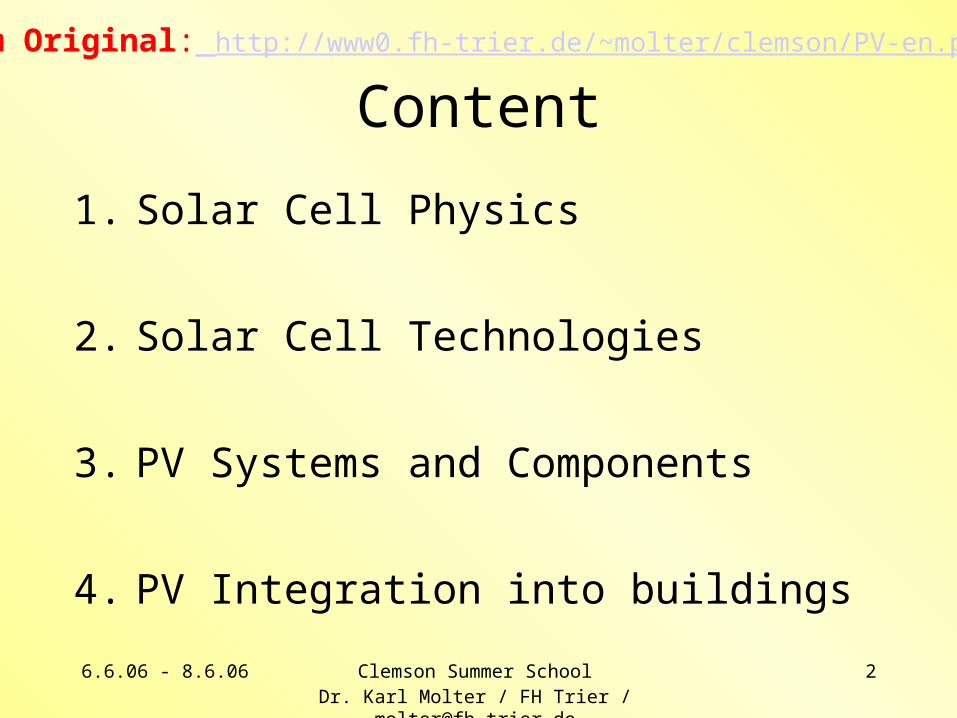
Content
1. Solar Cell Physics
2. Solar Cell Technologies
3. PV Systems and Components
4. PV Integration into buildings
Zum Original: http://www0.fh-trier.de/~molter/clemson/PV-en.ppt
6.6.06 - 8.6.06 Clemson Summer School 3.
Ich benutze nur das Kaptel 1 „Solar Cells Physics“ und einige Folien aus Kapitel 2 (Materials).
Ich empfehle aber den gesamten Vortrag von Dr. Molter:
Zum Original: http://www0.fh-trier.de/~molter/clemson/PV-en.ppt
6.6.06 - 8.6.06 Clemson Summer SchoolDr. Karl Molter / FH Trier / [email protected]
4
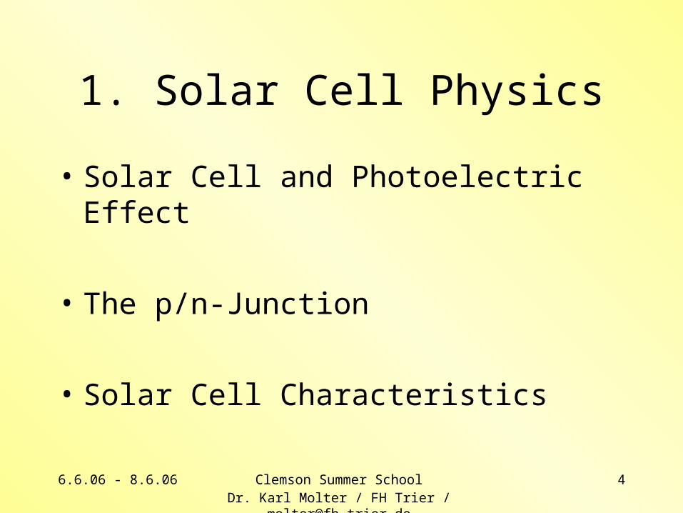
1. Solar Cell Physics
• Solar Cell and Photoelectric Effect
• The p/n-Junction
• Solar Cell Characteristics
6.6.06 - 8.6.06 Clemson Summer SchoolDr. Karl Molter / FH Trier / [email protected]
5
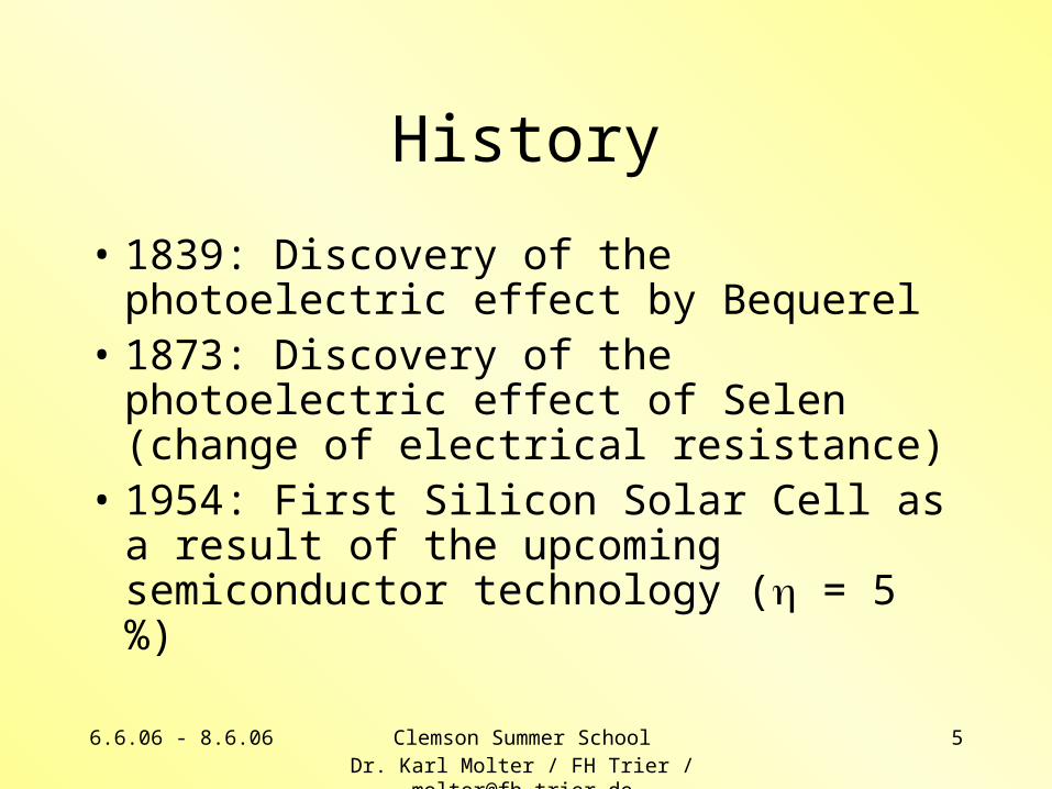
History
• 1839: Discovery of the photoelectric effect by Bequerel
• 1873: Discovery of the photoelectric effect of Selen (change of electrical resistance)
• 1954: First Silicon Solar Cell as a result of the upcoming semiconductor technology ( = 5 %)
6.6.06 - 8.6.06 Clemson Summer SchoolDr. Karl Molter / FH Trier / [email protected]
6
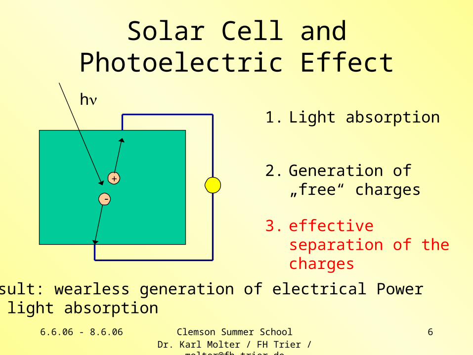
Solar Cell and Photoelectric Effect
1. Light absorptionh
-
+2. Generation of „free“
charges
3. effective separation of the charges
Result: wearless generation of electrical Power by light absorption
6.6.06 - 8.6.06 Clemson Summer SchoolDr. Karl Molter / FH Trier / [email protected]
7
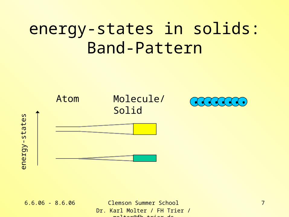
energy-states in solids:Band-Pattern
Atom Molecule/Solid
ener
gy-s
tate
s
• • • • • • • •
6.6.06 - 8.6.06 Clemson Summer SchoolDr. Karl Molter / FH Trier / [email protected]
8
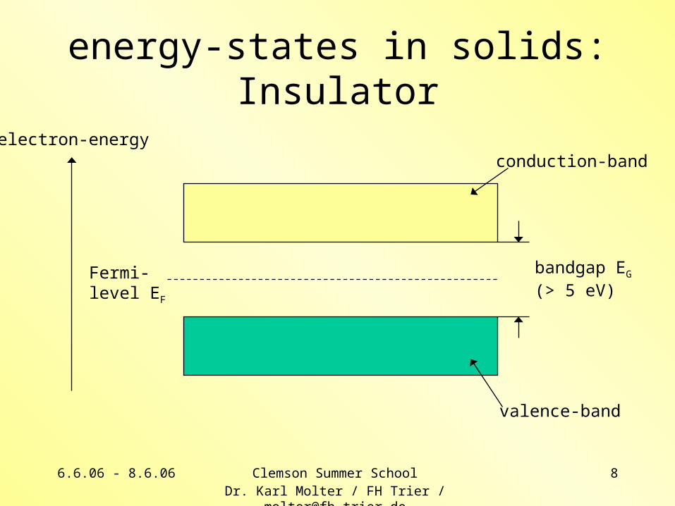
energy-states in solids:Insulator
electron-energyconduction-band
valence-band
Fermi-level EF
bandgap EG
(> 5 eV)
6.6.06 - 8.6.06 Clemson Summer SchoolDr. Karl Molter / FH Trier / [email protected]
9
Terms:
Fermilevel EF: limit between occupied and non occupied energy-states at T = 0 K (absolute zero)
valence-band: completely occupied energy-band just be-
low the Ferminiveau at T = 0 K, theelectrons are „fixed“ inside the atomic structure
conduction-band:energy-band just above the valence-band, the electrons can move „freely“
bandgap EG: distance between valance-band andconduction band
6.6.06 - 8.6.06 Clemson Summer SchoolDr. Karl Molter / FH Trier / [email protected]
10
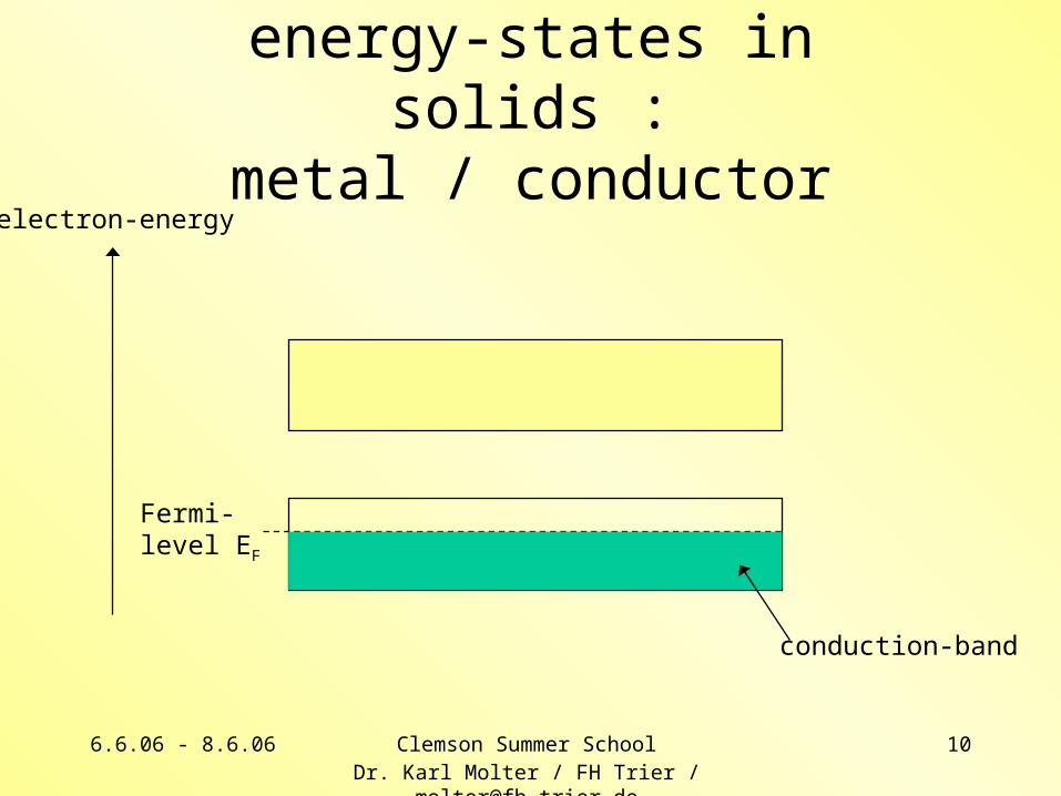
energy-states in solids :metal / conductor
electron-energy
conduction-band
Fermi-level EF
6.6.06 - 8.6.06 Clemson Summer SchoolDr. Karl Molter / FH Trier / [email protected]
11
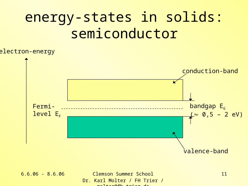
energy-states in solids:semiconductor
electron-energy
conduction-band
valence-band
Fermi-level EF
bandgap EG
( 0,5 – 2 eV)
6.6.06 - 8.6.06 Clemson Summer SchoolDr. Karl Molter / FH Trier / [email protected]
12
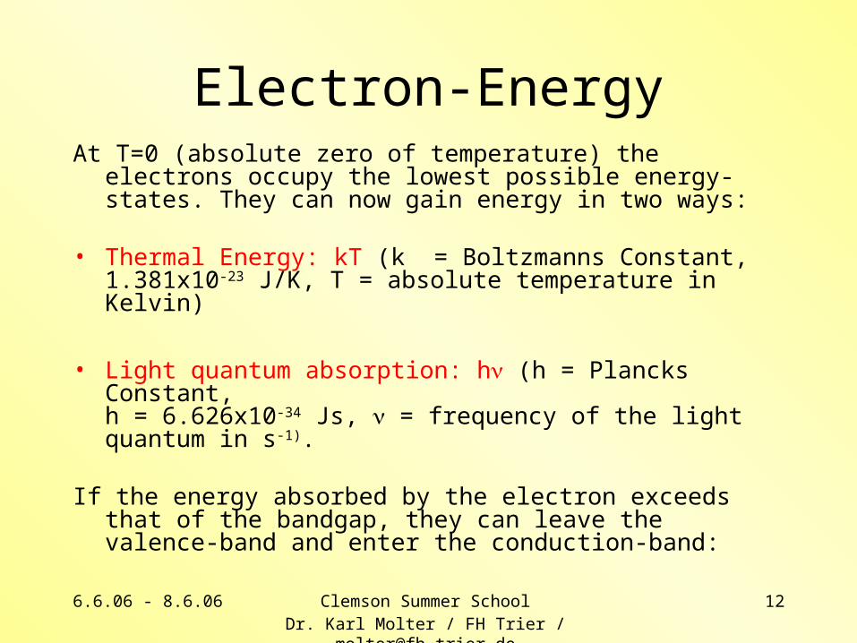
Electron-EnergyAt T=0 (absolute zero of temperature) the electrons occupy the
lowest possible energy-states. They can now gain energy in two ways:
• Thermal Energy: kT (k = Boltzmanns Constant, 1.381x10⁻²³ J/K, T = absolute temperature in Kelvin)
• Light quantum absorption: h (h = Plancks Constant, h = 6.626x10⁻³⁴ Js, = frequency of the light quantum in s-1).
If the energy absorbed by the electron exceeds that of the bandgap, they can leave the valence-band and enter the conduction-band:
6.6.06 - 8.6.06 Clemson Summer SchoolDr. Karl Molter / FH Trier / [email protected]
13
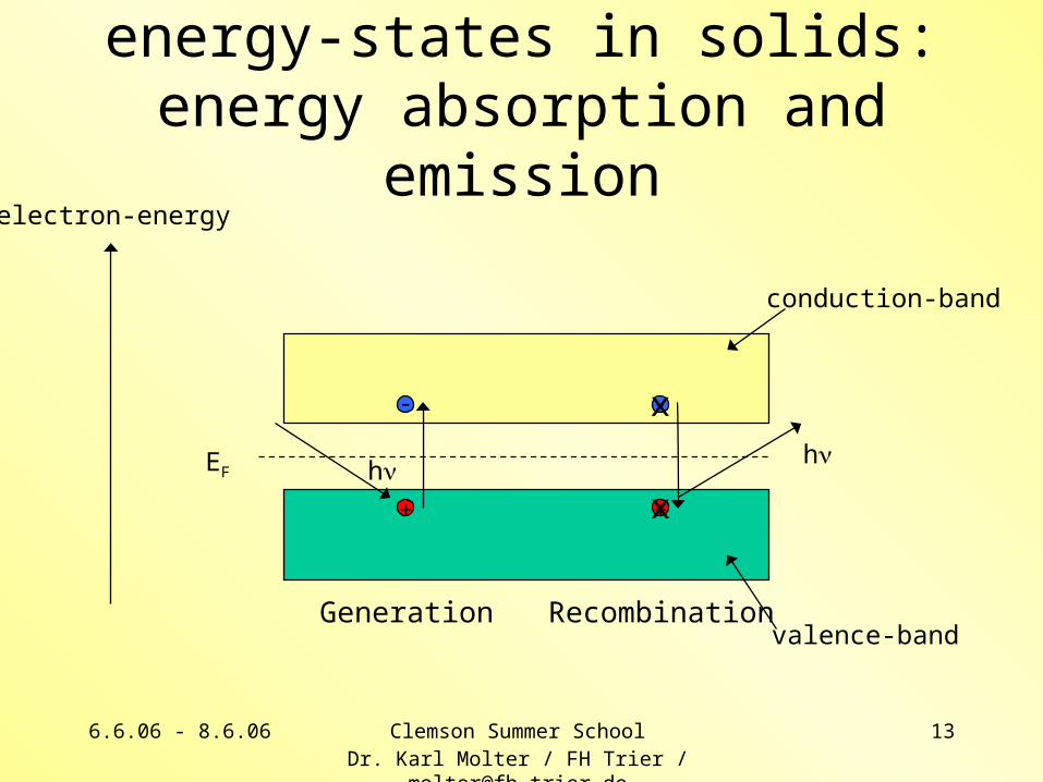
energy-states in solids:energy absorption and emission
electron-energy
conduction-band
valence-band
EF
+
-
h
Generation
+
-
h
Recombination
x
x
6.6.06 - 8.6.06 Clemson Summer SchoolDr. Karl Molter / FH Trier / [email protected]
14
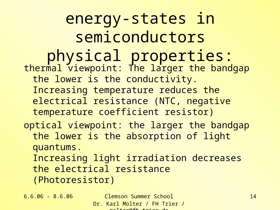
energy-states in semiconductorsphysical properties:
thermal viewpoint: The larger the bandgap the lower is the conductivity. Increasing temperature reduces the electrical resistance (NTC, negative temperature coefficient resistor)
optical viewpoint: the larger the bandgap the lower is the absorption of light quantums. Increasing light irradiation decreases the electrical resistance (Photoresistor)
6.6.06 - 8.6.06 Clemson Summer SchoolDr. Karl Molter / FH Trier / [email protected]
15
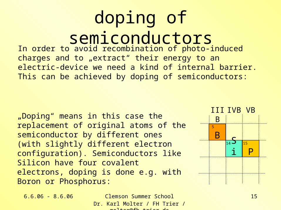
doping of semiconductorsIn order to avoid recombination of photo-induced charges and to „extract“ their energy to an electric-device we need a kind of internal barrier. This can be achieved by doping of semiconductors:
IIIB IVB VB
Si14
B 5
P15
„Doping“ means in this case the replacement of original atoms of the semiconductor by different ones (with slightly different electron configuration). Semiconductors like Silicon have four covalent electrons, doping is done e.g. with Boron or Phosphorus:
6.6.06 - 8.6.06 Clemson Summer SchoolDr. Karl Molter / FH Trier / [email protected]
16
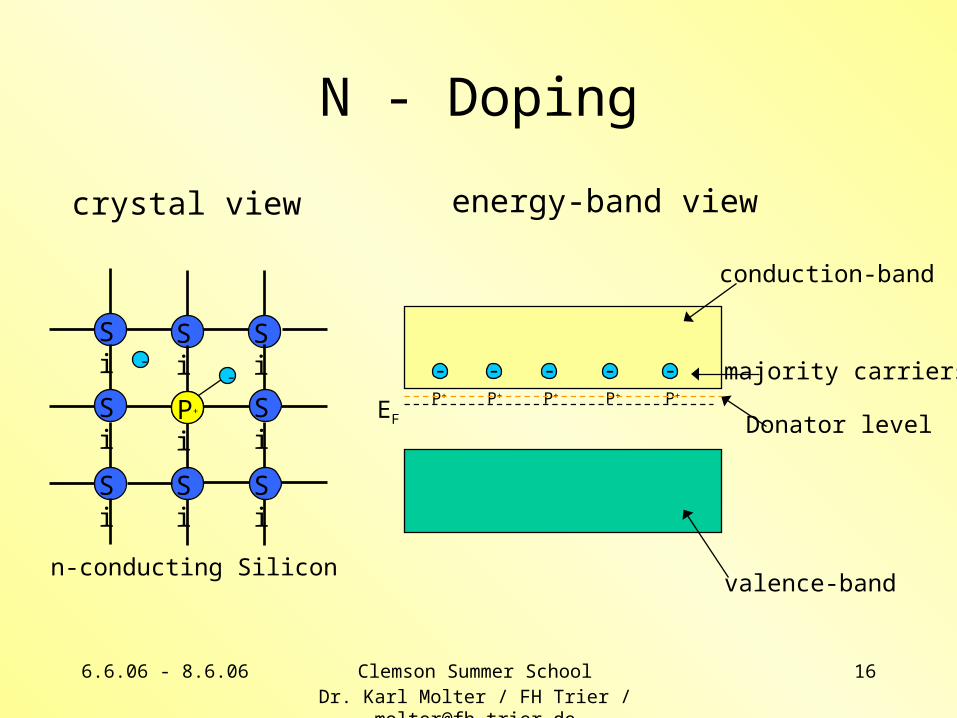
N - Doping
Si Si
Si
Si
Si
Si
Si
Si
Si
P+
-
n-conducting Silicon
-
crystal view
conduction-band
valence-band
EF
- - - - -P+ P+ P+ P+ P+
majority carriers
Donator level
energy-band view
6.6.06 - 8.6.06 Clemson Summer SchoolDr. Karl Molter / FH Trier / [email protected]
17
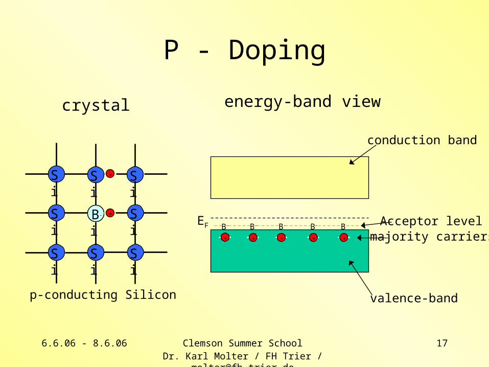
P - Doping
Si Si
Si
Si
Si
Si
Si
Si
Si
p-conducting Silicon
B- +
+
crystal
conduction band
valence-band
EF B- B- B- B- B-
majority carriersAcceptor level
+ + + + +
energy-band view
6.6.06 - 8.6.06 Clemson Summer SchoolDr. Karl Molter / FH Trier / [email protected]
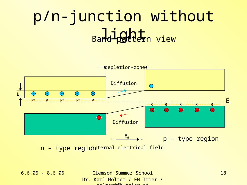
18
p – type region
EFB- B- B- B- B-
+ + + +
n – type region
- - - -P+ P+ P+ P+ P+
p/n-junction without lightBand pattern view
+
--Diffusion
+
Diffusion
internal electrical field
+ -Ed
Ud
depletion-zone
6.6.06 - 8.6.06 Clemson Summer SchoolDr. Karl Molter / FH Trier / [email protected]
19
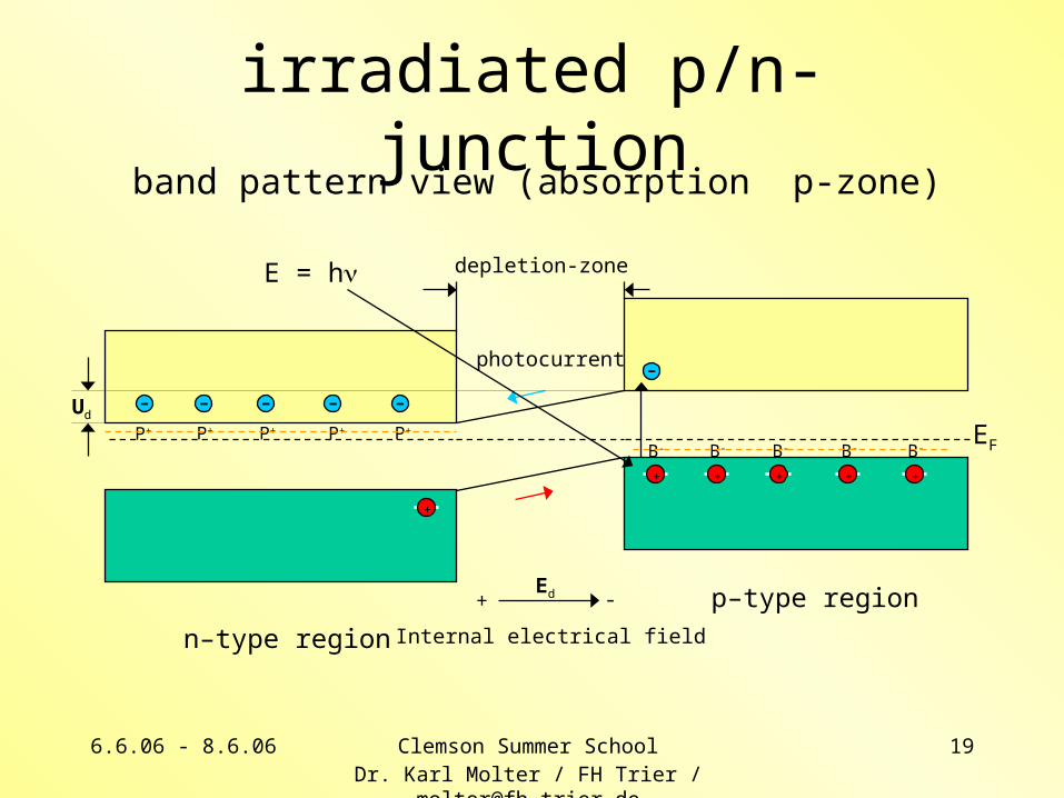
p–type region
EFB- B- B- B- B-
+ + + +
n–type region
- - - -P+ P+ P+ P+ P+
irradiated p/n-junctionband pattern view (absorption p-zone)
+
-
+
photocurrent
Internal electrical field
+ -Ed
Ud
depletion-zoneE = h
-
6.6.06 - 8.6.06 Clemson Summer SchoolDr. Karl Molter / FH Trier / [email protected]
20
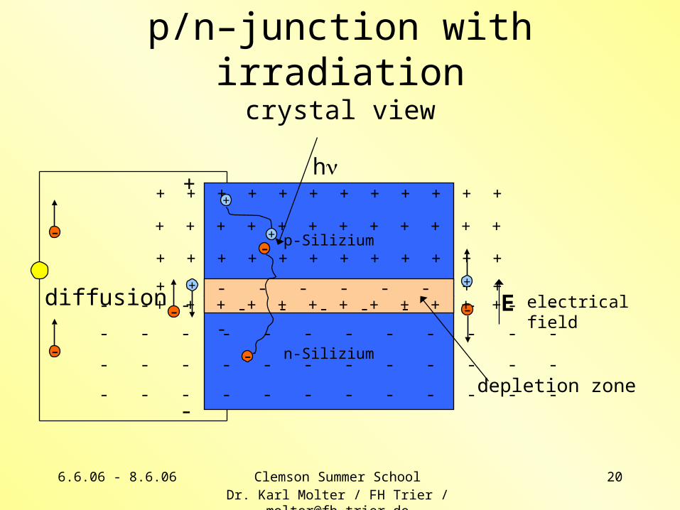
p/n–junction with irradiationcrystal view
n-Silizium
- - - - - - - - - - - -
- - - - - - - - - - - -
- - - - - - - - - - - -
- - - - - - - - - - - -
p-Silizium
+ + + + + + + + + + + +
+ + + + + + + + + + + +
+ + + + + + + + + + + +
+ + + + + + + + + + + +
+
-diffusion
-
+
electrical fieldE- - - - - - - - - - - -+ + + + + + + + + + + +
+-
h
-
+
-
-
-
+
depletion zone
6.6.06 - 8.6.06 Clemson Summer SchoolDr. Karl Molter / FH Trier / [email protected]
21
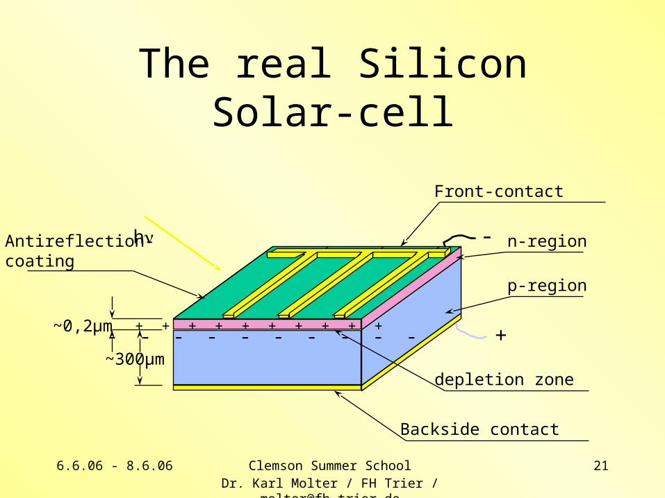
Antireflection-coating
The real Silicon Solar-cell
~0,2µm
~300µm
Front-contact
Backside contact
n-region
p-region
-
+
h
depletion zone
- - - - - - - - - -+ + + + + + + + + +
6.6.06 - 8.6.06 Clemson Summer SchoolDr. Karl Molter / FH Trier / [email protected]
22
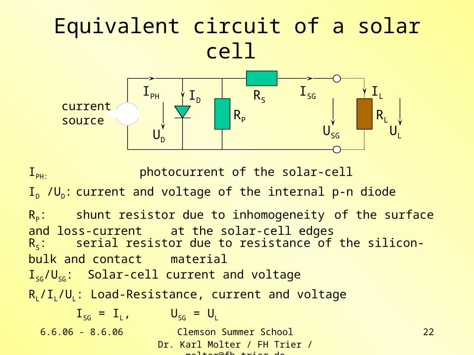
Equivalent circuit of a solar cell
RP
USG
RSISG
RL
UL
ILID
UD
currentsource
IPH
IPH: photocurrent of the solar-cell
ID /UD: current and voltage of the internal p-n diode
RP: shunt resistor due to inhomogeneity of the surface and loss-current at the solar-cell edges
RS: serial resistor due to resistance of the silicon-bulk and contact materialISG/USG: Solar-cell current and voltage
RL/IL/UL: Load-Resistance, current and voltage
ISG = IL, USG = UL
6.6.06 - 8.6.06 Clemson Summer SchoolDr. Karl Molter / FH Trier / [email protected]
23
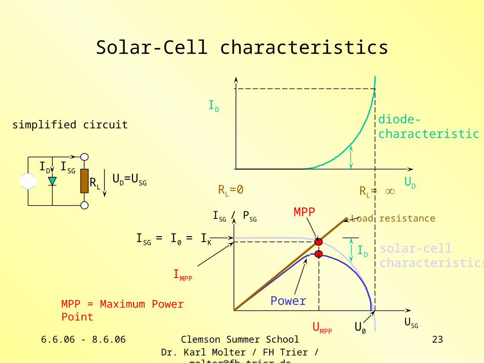
Solar-Cell characteristics
ID ISG
RLUD=USG
ID
ISG / PSG
USG
solar-cellcharacteristics
ISG = I0 = IK
RL=0 RL=
Power
UD
diode-characteristic
ID
U0
Load resistance
UMPP
MPP
IMPP
MPP = Maximum Power Point
simplified circuit
6.6.06 - 8.6.06 Clemson Summer SchoolDr. Karl Molter / FH Trier / [email protected]
24
Solar-cell characteristics
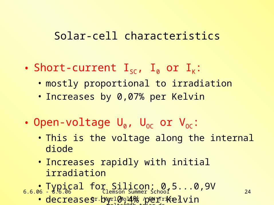
• Short-current ISC, I0 or IK:• mostly proportional to irradiation• Increases by 0,07% per Kelvin
• Open-voltage U0, UOC or VOC:• This is the voltage along the internal diode• Increases rapidly with initial irradiation• Typical for Silicon: 0,5...0,9V• decreases by 0,4% per Kelvin
6.6.06 - 8.6.06 Clemson Summer SchoolDr. Karl Molter / FH Trier / [email protected]
25
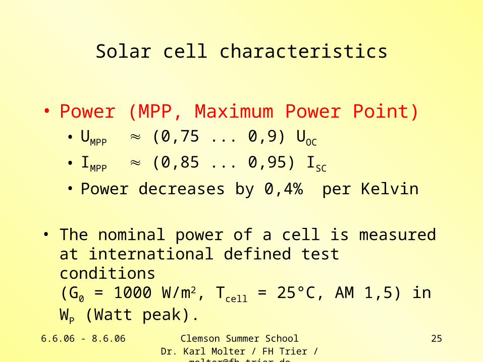
Solar cell characteristics
• Power (MPP, Maximum Power Point)• UMPP (0,75 ... 0,9) UOC
• IMPP (0,85 ... 0,95) ISC
• Power decreases by 0,4% per Kelvin
• The nominal power of a cell is measured at international defined test conditions(G0 = 1000 W/m2, Tcell = 25°C, AM 1,5) in WP (Watt peak).
6.6.06 - 8.6.06 Clemson Summer SchoolDr. Karl Molter / FH Trier / [email protected]
26
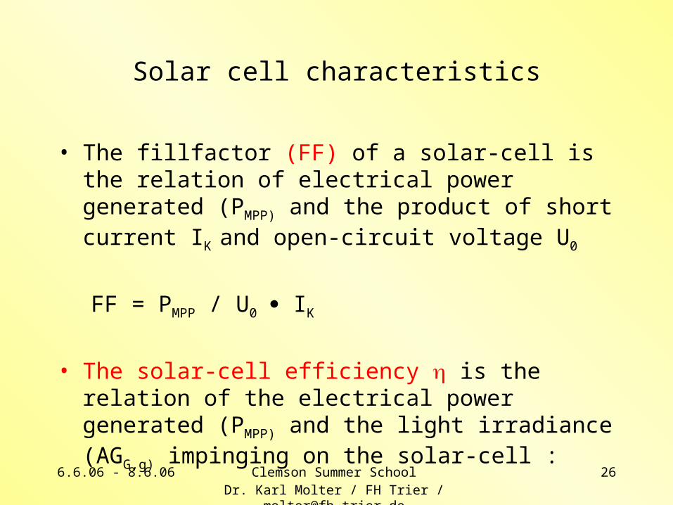
Solar cell characteristics
• The fillfactor (FF) of a solar-cell is the relation of electrical power generated (PMPP) and the product of short current IK and open-circuit voltage U0
FF = PMPP / U0 IK
• The solar-cell efficiency is the relation of the electrical power generated (PMPP) and the light irradiance (AGG,g) impinging on the solar-cell :
= PMPP / AGG,g
6.6.06 - 8.6.06 Clemson Summer SchoolDr. Karl Molter / FH Trier / [email protected]
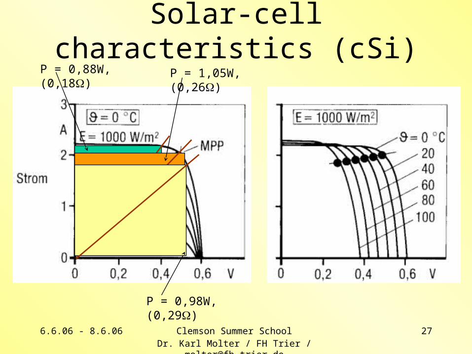
27
Solar-cell characteristics (cSi)P = 0,88W, (0,18) P = 1,05W, (0,26)
P = 0,98W, (0,29)
6.6.06 - 8.6.06 Clemson Summer SchoolDr. Karl Molter / FH Trier / [email protected]
28
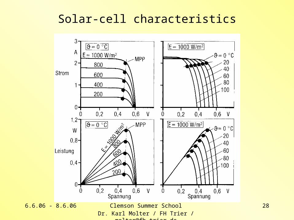
Solar-cell characteristics
6.6.06 - 8.6.06 Clemson Summer SchoolDr. Karl Molter / FH Trier / [email protected]
29
Zu den weiteren Folien bitte Dr. Molter‘s homepage besuchen:
Zum Original: http://www0.fh-trier.de/~molter/clemson/PV-en.ppt
6.6.06 - 8.6.06 Clemson Summer SchoolDr. Karl Molter / FH Trier / [email protected]
30
This Powerpoint Presentation can be downloadedfrom:
www.fh-trier.de/~molter
www.fh-trier.de/~molter
Recommended