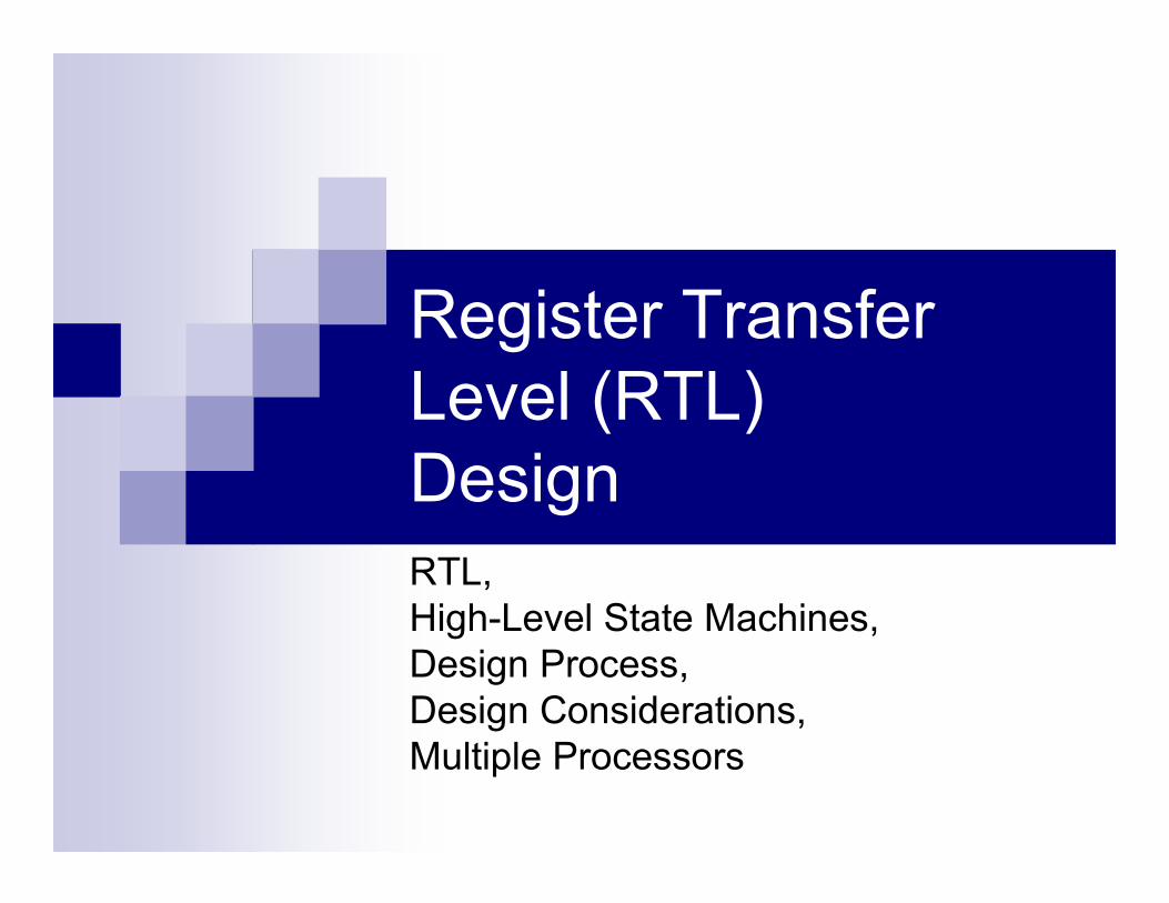
Register Transfer
Level (RTL)
Design
RTL,
High-Level State Machines,
Design Process,
Design Considerations,
Multiple Processors
High Level Sequential Behavior
� Finite state machines can be used to
capture simple sequential behavior using
bit inputs
� High level state machines can be used to
capture more complex logic involving
multi-bit variables.
)
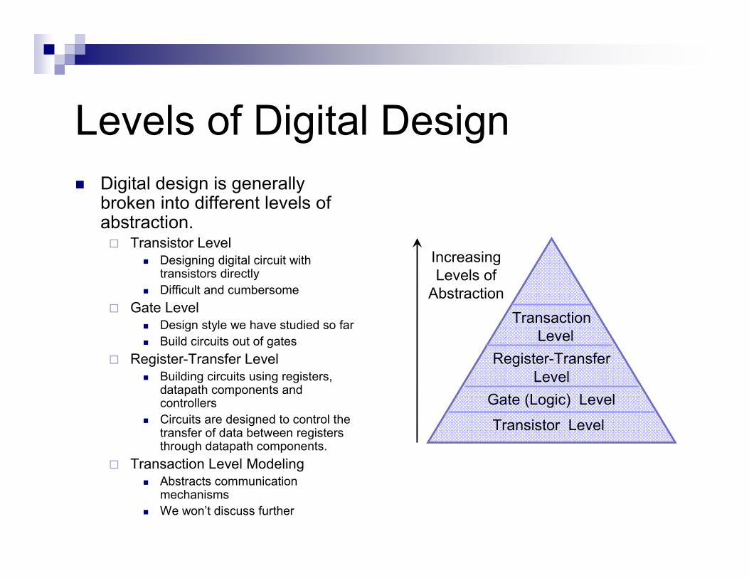
Levels of Digital Design
� Digital design is generally broken into different levels of abstraction.� Transistor Level
� Designing digital circuit with transistors directly
� Difficult and cumbersome
� Gate Level
� Design style we have studied so far
� Build circuits out of gates
� Register-Transfer Level
� Building circuits using registers, datapath components and controllers
� Circuits are designed to control the transfer of data between registers through datapath components.
� Transaction Level Modeling
� Abstracts communication mechanisms
� We won’t discuss further
Transistor Level
Gate (Logic) Level
Register-Transfer
Level
Transaction
Level
Increasing
Levels of
Abstraction
)
Processors
� ‘Processor’ is a generic term for a circuit designed using RTL principles� Programmable Processor
� A generic processor designed that can run programs
� I.E. Intel Processors
� Custom Processor� Specialized design that implements specific functionality
� I.E. A circuit to process digital TV signals.
� Processors can be designed using high level state machines
)
High Level State Machines
� High Level State Machines (HLSM) extend FSMs with
features that make it possible to capture more complex
behaviors.
� Multi-bit data inputs and outputs
� Assumed unsigned unless specified as signed
� Local storage
� Registers loaded on rising clock edges (i.e. when leaving a state)
� Arithmetic operations
� Add, Multiply, Compare, Bit Shift, etc.
)
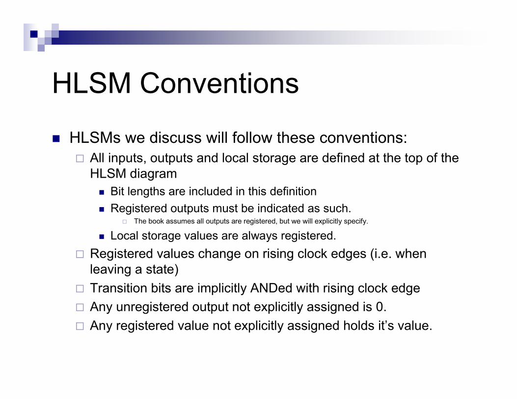
HLSM Conventions
� HLSMs we discuss will follow these conventions:
� All inputs, outputs and local storage are defined at the top of the
HLSM diagram
� Bit lengths are included in this definition
� Registered outputs must be indicated as such.� The book assumes all outputs are registered, but we will explicitly specify.
� Local storage values are always registered.
� Registered values change on rising clock edges (i.e. when
leaving a state)
� Transition bits are implicitly ANDed with rising clock edge
� Any unregistered output not explicitly assigned is 0.
� Any registered value not explicitly assigned holds it’s value.
)
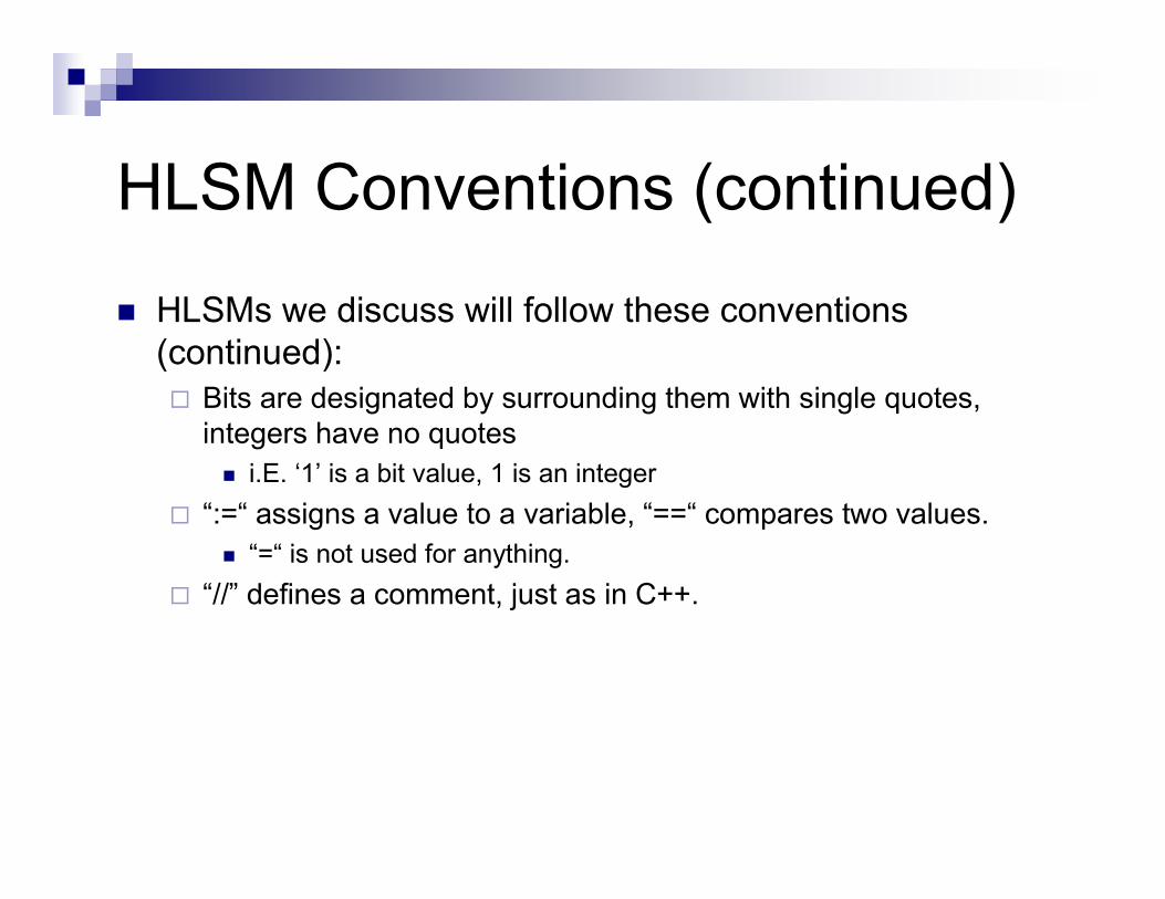
HLSM Conventions (continued)
� HLSMs we discuss will follow these conventions
(continued):
� Bits are designated by surrounding them with single quotes,
integers have no quotes
� i.E. ‘1’ is a bit value, 1 is an integer
� “:=“ assigns a value to a variable, “==“ compares two values.
� “=“ is not used for anything.
� “//” defines a comment, just as in C++.
)
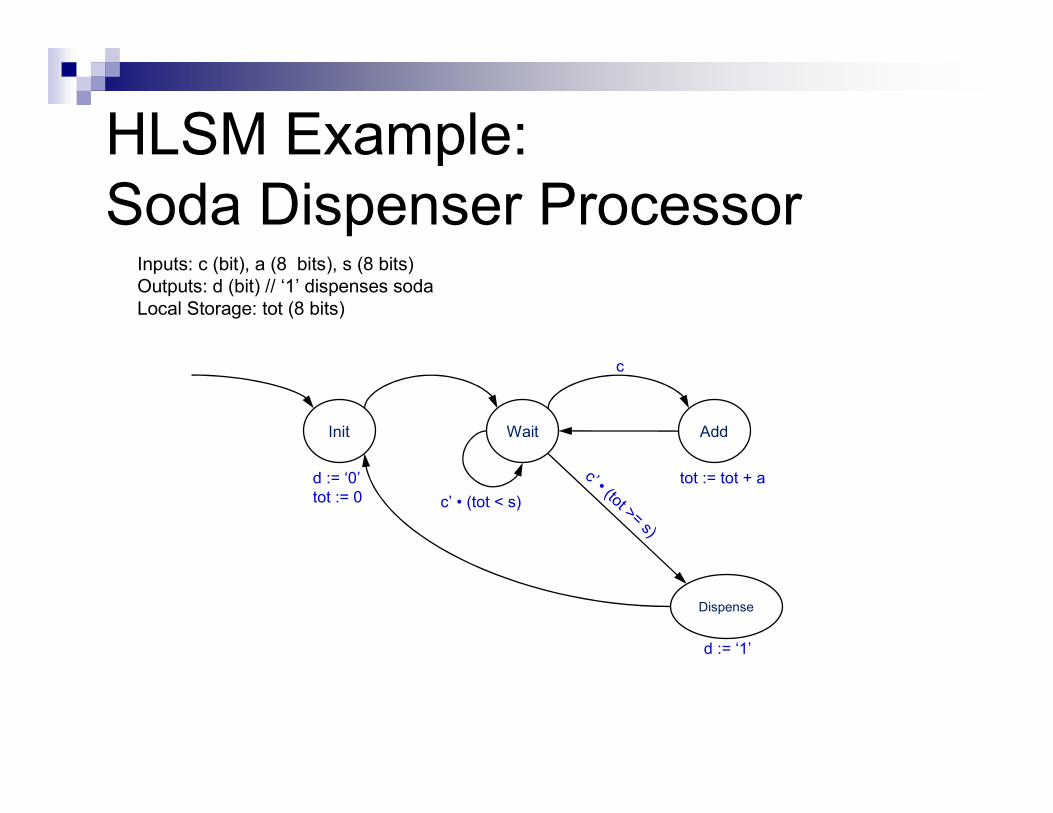
HLSM Example:
Soda Dispenser Processor
Init Wait Add
Dispense
c
d := ‘1’
tot := tot + a
c’ • (tot < s)
d := ‘0’
tot := 0
c’ • (tot >= s)
Inputs: c (bit), a (8 bits), s (8 bits)
Outputs: d (bit) // ‘1’ dispenses soda
Local Storage: tot (8 bits)
)
A Word of Warning About
Registered Outputs� Clocked storage items are not updated in the
same clock cycle that their control signals are set
� Must wait for a rising clock edge for the register to obtain a new value.
� Note: The register control bits set up in a state prepare the value on the register inputs to be captured on the next clock cycle!
� Example: In the previous example, when is the value of tot reset to 0?
)
HLSM Example:
8-bit Up/Down Counter
� Design an HLSM for an 8-bit up/down
counter
�What are the inputs
�What are the outputs?
�What are the internal variables (if any)?
�Draw the HLSM
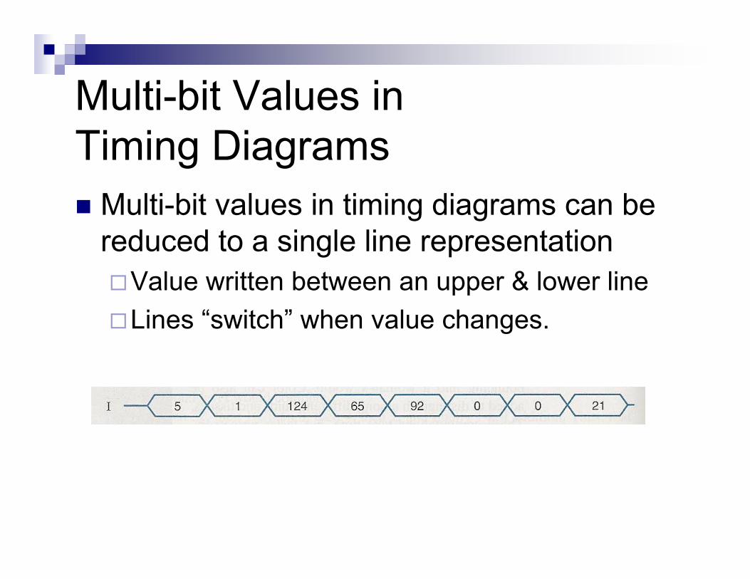
Multi-bit Values in
Timing Diagrams
� Multi-bit values in timing diagrams can be
reduced to a single line representation
�Value written between an upper & lower line
�Lines “switch” when value changes.
)
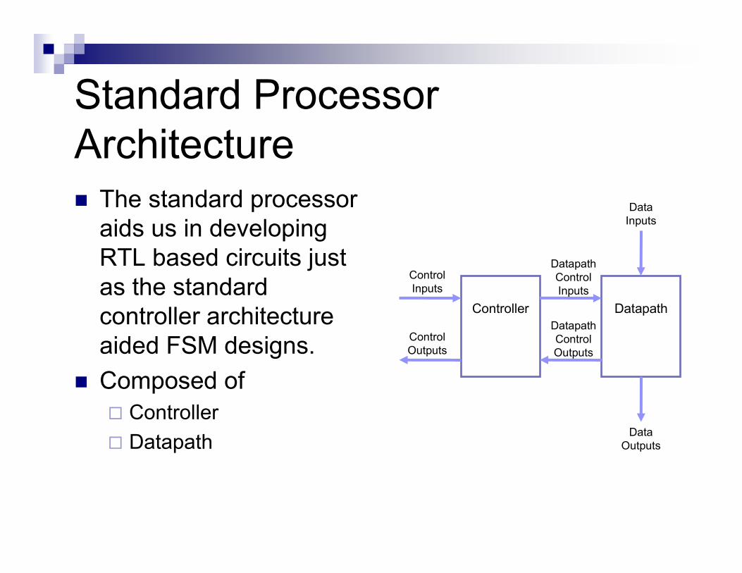
Standard Processor
Architecture
� The standard processor
aids us in developing
RTL based circuits just
as the standard
controller architecture
aided FSM designs.
� Composed of
� Controller
� Datapath
Controller Datapath
Control
Inputs
Control
Outputs
Datapath
Control
Inputs
Datapath
Control
Outputs
Data
Inputs
Data
Outputs
)
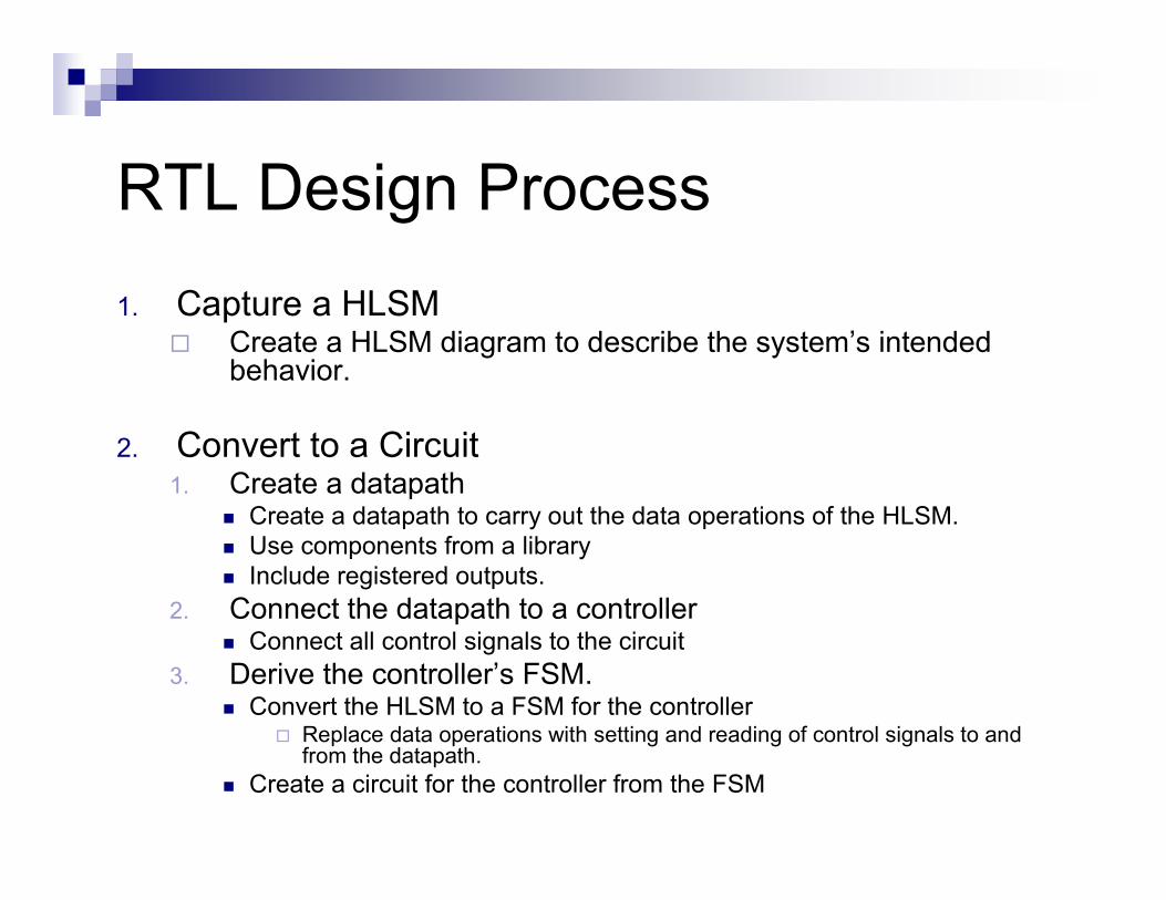
RTL Design Process
1. Capture a HLSM� Create a HLSM diagram to describe the system’s intended
behavior.
2. Convert to a Circuit1. Create a datapath
� Create a datapath to carry out the data operations of the HLSM.
� Use components from a library
� Include registered outputs.
2. Connect the datapath to a controller� Connect all control signals to the circuit
3. Derive the controller’s FSM.� Convert the HLSM to a FSM for the controller
� Replace data operations with setting and reading of control signals to and from the datapath.
� Create a circuit for the controller from the FSM
)
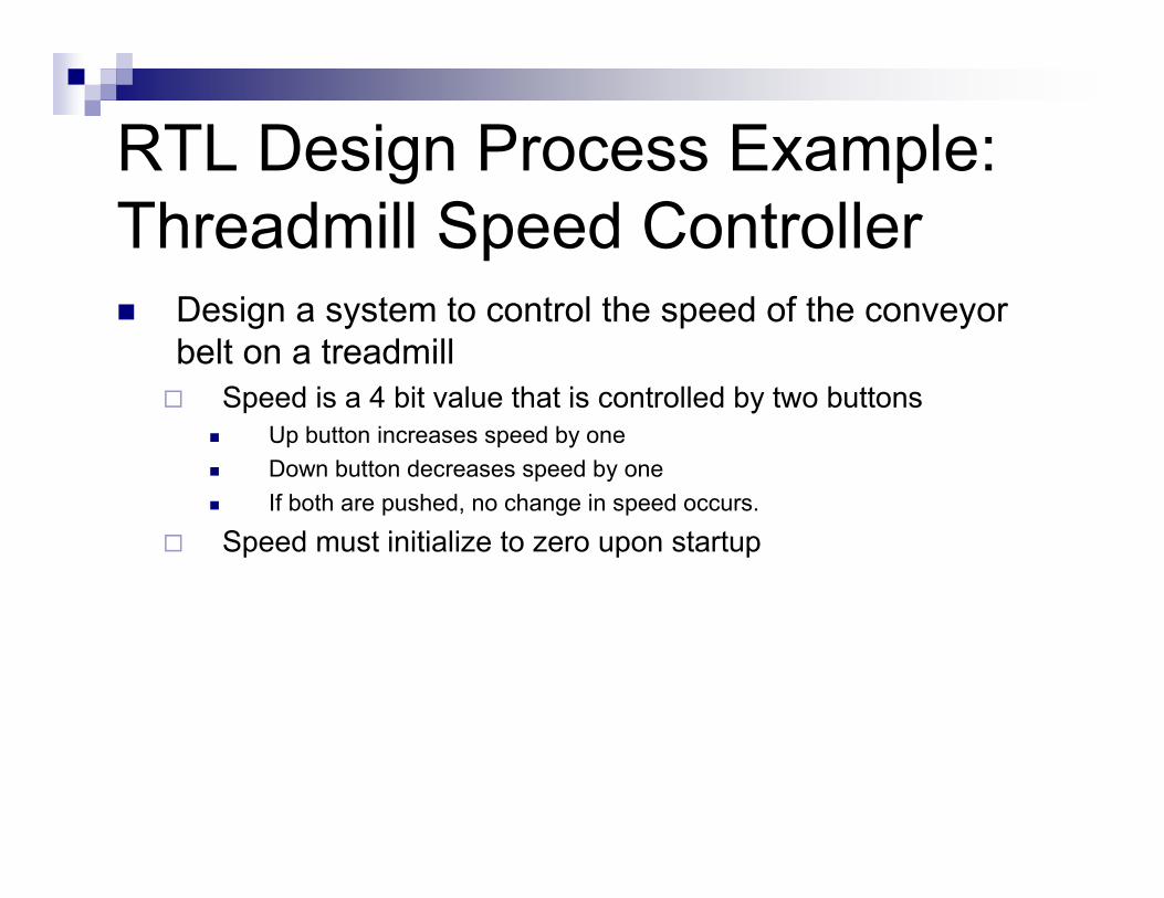
RTL Design Process Example:
Threadmill Speed Controller� Design a system to control the speed of the conveyor
belt on a treadmill
� Speed is a 4 bit value that is controlled by two buttons
� Up button increases speed by one
� Down button decreases speed by one
� If both are pushed, no change in speed occurs.
� Speed must initialize to zero upon startup

)
RTL Design Process Example:
Threadmill Speed Controller1. Capture a HLSM
� Create a HLSM diagram to describe the system’s intended behavior.
wait
Incr/
Init/
Inputs: up (bit), down (bit)
Outputs: speed (4 bit reg)
Internal Storage: n/a
Speed := 0
Speed := Speed - 1
Speed := Speed + 1
UP • DOWN’
(UP ⊕ DOWN)’
decr/
UP’ • DOWN
DOWN
UP
UP’ • DOWN
UP • DOWN’
UP’ • DOWN’
UP’ • DOWN’
)
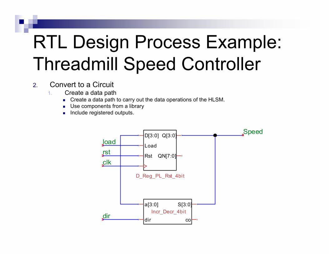
RTL Design Process Example:
Threadmill Speed Controller2. Convert to a Circuit
1. Create a data path� Create a data path to carry out the data operations of the HLSM.
� Use components from a library
� Include registered outputs.
rst
clk
dir
loadD[3:0] Q[3:0]
QN[7:0]
Load
Rst
D_Reg_PL_Rst_4bit
S[3:0]
co
a[3:0]
dir
Incr_Decr_4bit
Speed
)
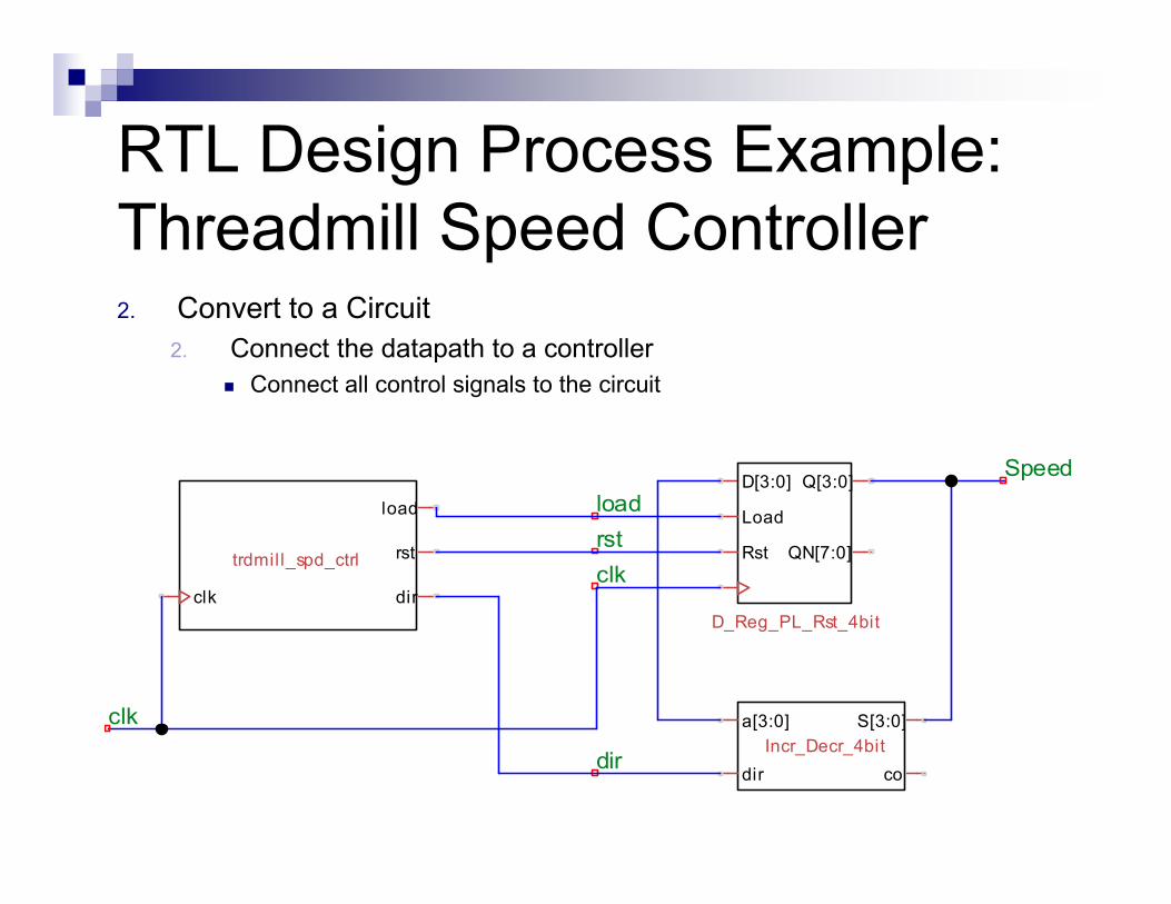
RTL Design Process Example:
Threadmill Speed Controller2. Convert to a Circuit
2. Connect the datapath to a controller
� Connect all control signals to the circuit
rst
clk
dir
loadD[3:0] Q[3:0]
QN[7:0]
Load
Rst
D_Reg_PL_Rst_4bit
S[3:0]
co
a[3:0]
dir
Incr_Decr_4bit
load
rst
dirclk
trdmill_spd_ctrl
clk
Speed
)
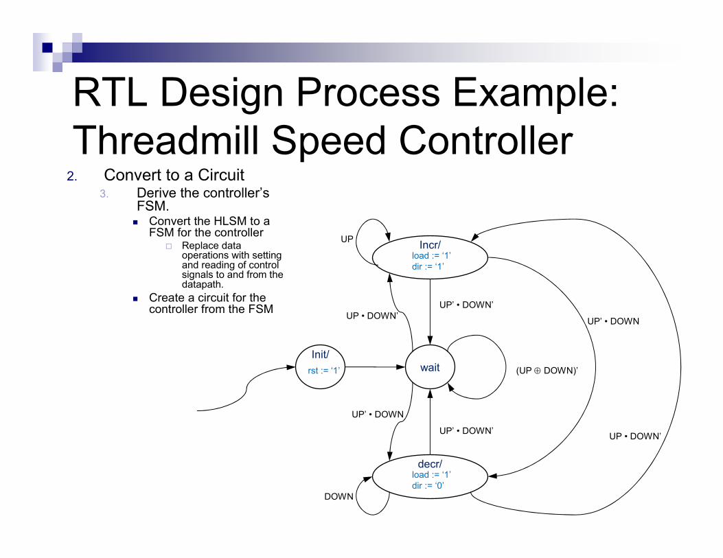
RTL Design Process Example:
Threadmill Speed Controller2. Convert to a Circuit
3. Derive the controller’s FSM.
� Convert the HLSM to a FSM for the controller
� Replace data operations with setting and reading of control signals to and from the datapath.
� Create a circuit for the controller from the FSM
wait
Incr/
Init/
UP • DOWN’
(UP ⊕ DOWN)’
decr/
UP’ • DOWN
DOWN
UP
UP’ • DOWN
UP • DOWN’
load := ‘1’
dir := ‘1’
load := ‘1’
dir := ‘0’
rst := ‘1’
UP’ • DOWN’
UP’ • DOWN’
)
Arrays in an HLSM
� An array is an ordered list of items.
� An array can be used in an HLSM just as it
is in C
�Use the array[index] notation.
�The first index in an array is 0.
� An array in a HLSM corresponds to a
register file or memory in a real circuit
)
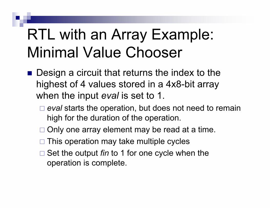
RTL with an Array Example:
Minimal Value Chooser
� Design a circuit that returns the index to the
highest of 4 values stored in a 4x8-bit array
when the input eval is set to 1.
� eval starts the operation, but does not need to remain
high for the duration of the operation.
� Only one array element may be read at a time.
� This operation may take multiple cycles
� Set the output fin to 1 for one cycle when the
operation is complete.
ꇰЋ
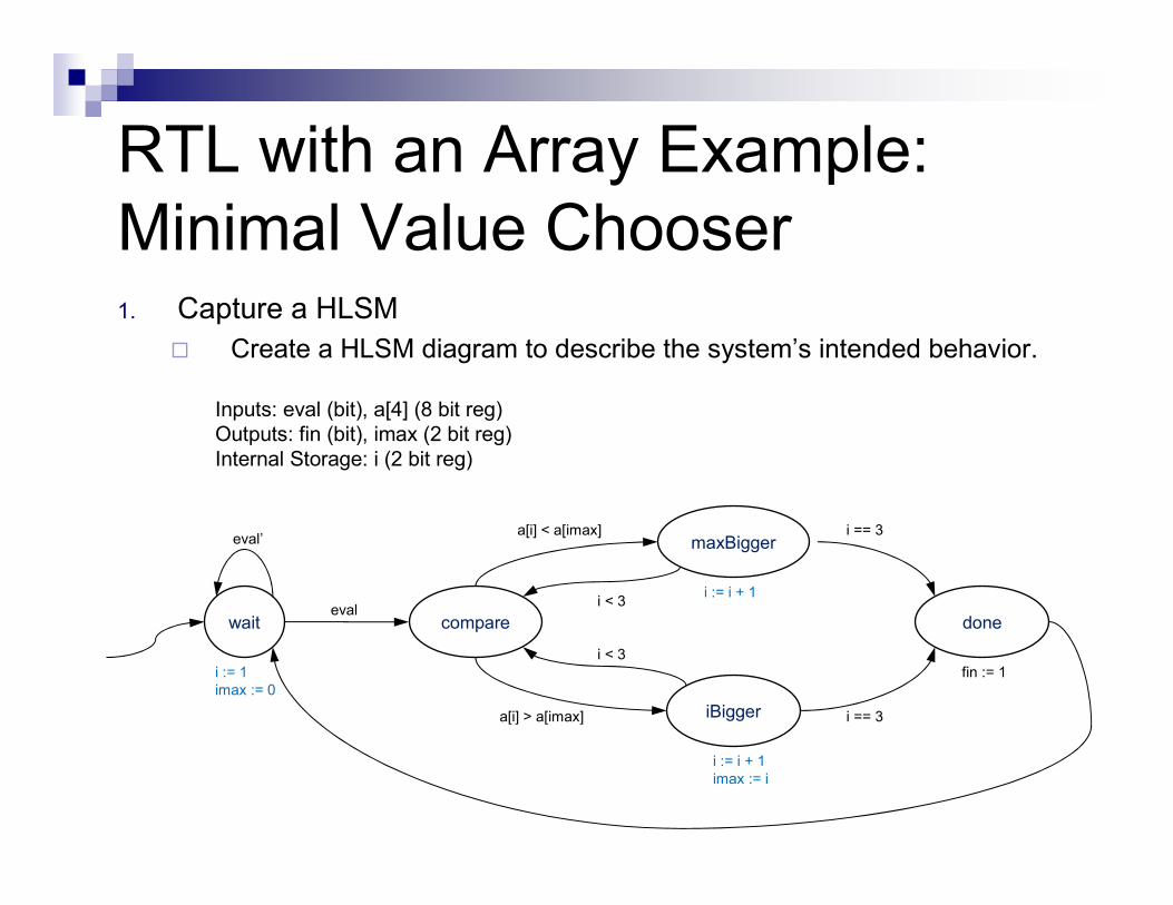
RTL with an Array Example:
Minimal Value Chooser1. Capture a HLSM
� Create a HLSM diagram to describe the system’s intended behavior.
Inputs: eval (bit), a[4] (8 bit reg)
Outputs: fin (bit), imax (2 bit reg)
Internal Storage: i (2 bit reg)
wait
i := 1
imax := 0
compare
maxBigger
iBigger
done
eval’
eval
a[i] < a[imax]
a[i] > a[imax]
i < 3
i < 3
i == 3
i == 3
i := i + 1
i := i + 1
imax := i
fin := 1
勠ЋD[3:0]
I0[3:0]
I1[3:0]S
D[3:0] Q[3:0]
QN[7:0]
Load
Rst
D[3:0] Q[3:0]
QN[7:0]
Load
Rst
S[3:0]
co
a[3:0]a b
out_gtout_eq
out_ltmagcomp
0x1
i_load
i_init
i
max_ld
max_init
imax
clk
0x3
i_lt_3
a b
out_gtout_eq
out_ltmagcomp
i_data
max_data
i_gt_max
i_lt_max
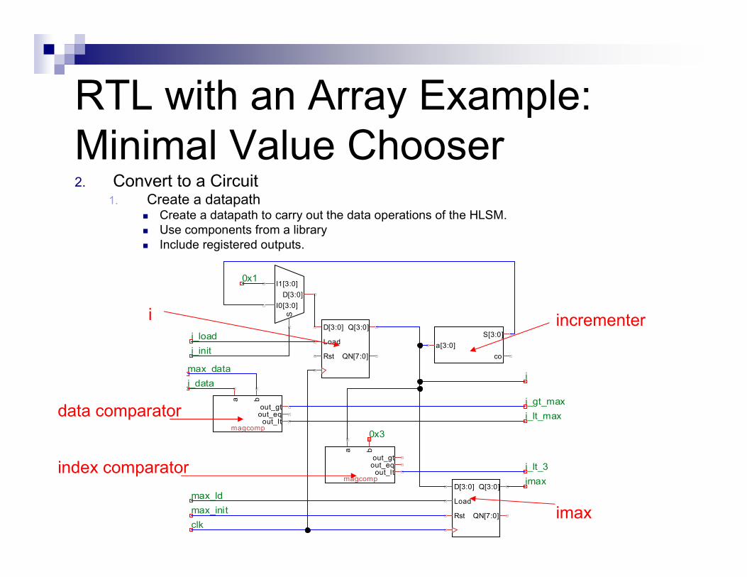
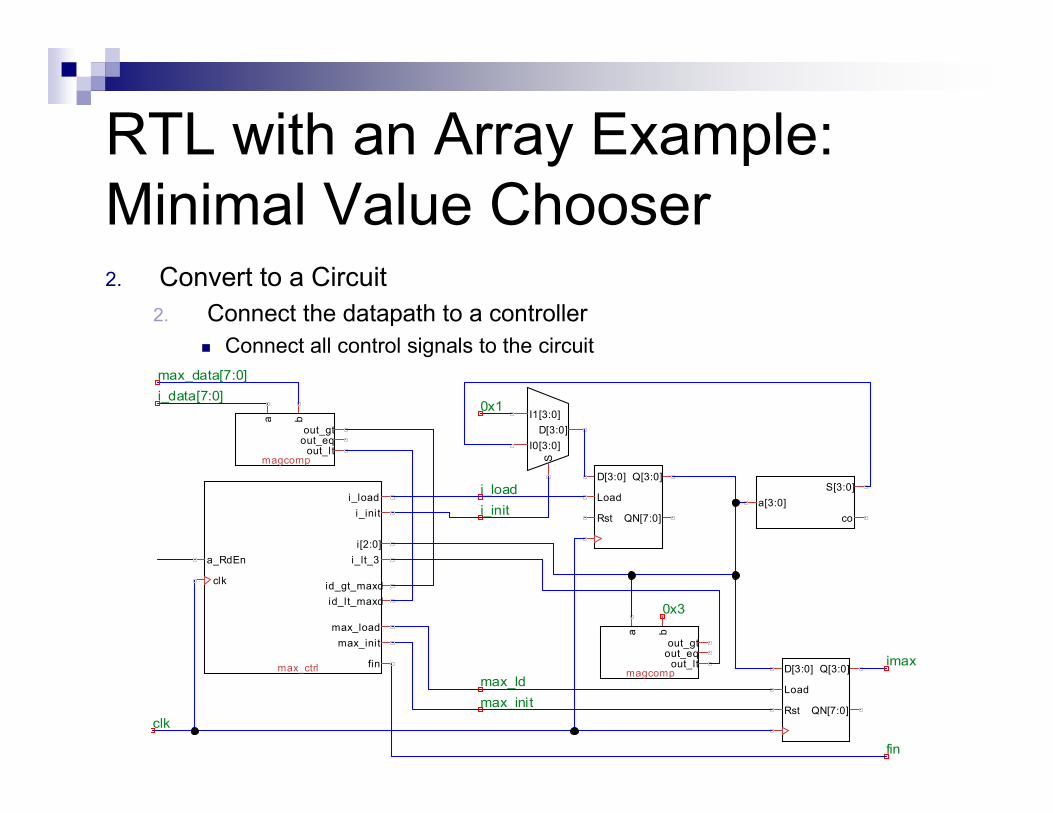
RTL with an Array Example:
Minimal Value Chooser2. Convert to a Circuit
1. Create a datapath� Create a datapath to carry out the data operations of the HLSM.
� Use components from a library
� Include registered outputs.
i incrementer
imax
data comparator
index comparator
埰А
RTL with an Array Example:
Minimal Value Chooser2. Convert to a Circuit
2. Connect the datapath to a controller
� Connect all control signals to the circuit
D[3:0] Q[3:0]
QN[7:0]
Load
Rst
D[3:0] Q[3:0]
QN[7:0]
Load
Rst
S[3:0]
co
a[3:0]
D[3:0]
I0[3:0]
I1[3:0]
S
clk
0x1
max_ld
max_init
i_load
i_init
imax
fin
a b
out_gtout_eq
out_ltmagcomp
0x3
a b
out_gtout_eq
out_ltmagcomp
a_RdEn
i_load
i_init
max_load
max_init
clk
i[2:0]
fin
i_lt_3
id_lt_maxd
id_gt_maxd
max_ctrl
i_data[7:0]
max_data[7:0]

~
RTL with an Array Example:
Minimal Value Chooser2. Convert to a Circuit
3. Derive the controller’s FSM.� Convert the HLSM to a FSM for the controller
� Replace data operations with setting and reading of control signals to and from the data path.
� Create a circuit for the controller from the FSM
wait
i _init := 1
i_load := 1
max_load := 1
max_init := 1
compare
maxBigger
iBigger
done
eval’
eval
i_lt_max == 1
i_gt_max == 1
i_lt_3 == 1
i_lt_3 = 0
i_load := 1
i_load := 1
max_load := 1
fin := 1A_RdEn := 1
i_lt_3 == 1
i_lt_3 = 0
~
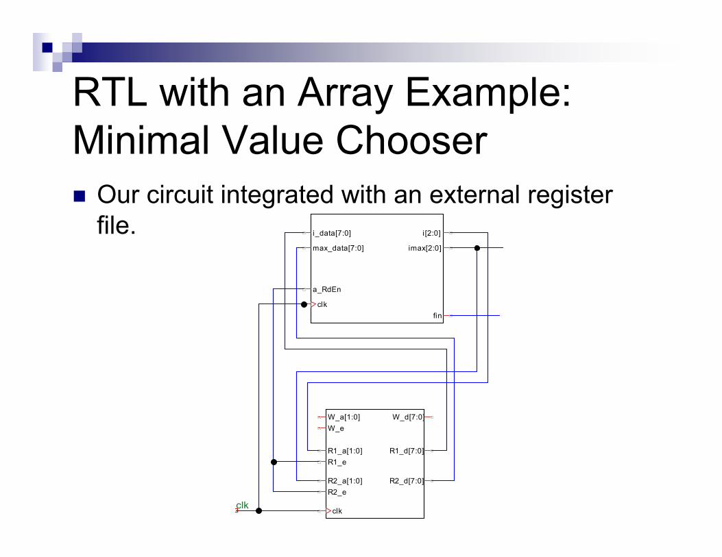
RTL with an Array Example:
Minimal Value Chooser
� Our circuit integrated with an external register
file.
R1_d[7:0]
clk
R1_e
W_d[7:0]
W_e
W_a[1:0]
R1_a[1:0]
R2_d[7:0]
R2_e
R2_a[1:0]
i_data[7:0]
max_data[7:0]
a_RdEn
clk
i[2:0]
imax[2:0]
fin
clk
낀Ћ
Multiple Processors
� Complex designs can be difficult to model with a single HLSM.
� A much simpler design methodology is to break the complex design up into multiple smaller processors.
� Global components can be shared between processors to facilitate this breakdown:�Signals
�Data path components
�Etc.
O
Multi-Processor Examples
� Example 1:
�Button debouncer processor used to
debounce mechanical button inputs to
another processor.
� Example 2:
�Reconsider the speed controller. How could it
be redesigned to allow two modes of
operation: manual control and oscillating?
Recommended