Te
st &
Mea
sure
men
t
Data
She
et |
08.0
0R&S®SMU200AVector Signal GeneratorSpecifications
SMU_dat-sw-en_0758-0197-22_v0800_Umschlag.indd 1 19.01.2012 11:55:11

Version 08.00, January 2012
2 Rohde & Schwarz R&S®SMU200A Vector Signal Generator
CONTENTS Introduction ..................................................................................................................................................................... 4 Key features .................................................................................................................................................................... 5 Frequency and enhancement options........................................................................................................................... 6
Frequency options ..................................................................................................................................................................................6 Enhancement options .............................................................................................................................................................................6
Modulation....................................................................................................................................................................... 7 Possible modulation types ......................................................................................................................................................................7 Simultaneous modulation........................................................................................................................................................................7
RF characteristics........................................................................................................................................................... 8 Frequency ...............................................................................................................................................................................................8 Frequency sweep....................................................................................................................................................................................8 Reference frequency...............................................................................................................................................................................8 Level .......................................................................................................................................................................................................9 Measured level data..............................................................................................................................................................................10 Level sweep ..........................................................................................................................................................................................11 Spectral purity .......................................................................................................................................................................................12 List mode ..............................................................................................................................................................................................14 Phase coherence (R&S®SMU-B90 option) ...........................................................................................................................................14
Analog modulation........................................................................................................................................................ 16 Internal modulation generator ...............................................................................................................................................................16 Input for external modulation signals ....................................................................................................................................................16 Amplitude modulation ...........................................................................................................................................................................16 Wideband amplitude modulation...........................................................................................................................................................16 Pulse modulation ..................................................................................................................................................................................17 Frequency modulation (R&S®SMU-B20 or R&S®SMU-B22 option)......................................................................................................17 Phase modulation (R&S®SMU-B20 or R&S®SMU-B22 option) ............................................................................................................17
I/Q modulation............................................................................................................................................................... 18 I/Q modulator ........................................................................................................................................................................................18 External wideband I/Q...........................................................................................................................................................................18 Internal baseband I/Q (with R&S®SMU-B13 option) .............................................................................................................................19 Differential I/Q output (R&S®SMU-B16 option) .....................................................................................................................................21 Digital baseband output (R&S®SMU-B18 option) .................................................................................................................................21 Baseband input (analog/digital) (R&S®SMU-B17 option) .....................................................................................................................22 I/Q baseband generator (R&S®SMU-B9/-B10/-B11 option) – arbitrary waveform mode ......................................................................24 I/Q baseband generator (R&S®SMU-B9/-B10/-B11 option) – realtime operation .................................................................................26 Modulation uncertainty for main standards ...........................................................................................................................................30 Signal performance for digital standards ..............................................................................................................................................30
Digital standards (for the R&S®SMU-B9/-B10/-B11 options) ..................................................................................... 34 Digital standards with external PC software or waveforms (for the R&S®SMU-B9/-B10/-B11 options) ................ 34

Version 08.00, January 2012
Rohde & Schwarz R&S®SMU200A Vector Signal Generator 3
Digital standards with R&S®WinIQSIM2™ (for the R&S®SMU-B9/-B10/-B11 ARB).................................................. 35 Fading and noise........................................................................................................................................................... 36
Fading simulator (R&S®SMU-B14 option) and fading simulator extension (R&S®SMU-B15 option)....................................................36 Dynamic fading and enhanced resolution (R&S®SMU-K71 option)......................................................................................................37 Extended statistic functions (R&S®SMU-K72 option)............................................................................................................................38 MIMO fading (R&S®SMU-K74 option)...................................................................................................................................................38 Dynamic scenario simulation (R&S®SMU-K77 option) .........................................................................................................................41 Additive white Gaussian noise (AWGN, R&S®SMU-K62 option) ..........................................................................................................41
Other options ................................................................................................................................................................ 42 BER measurement (R&S®SMU-K80 option).........................................................................................................................................42 BLER measurement (R&S®SMU-K80 option).......................................................................................................................................42
General data .................................................................................................................................................................. 43 Remote control......................................................................................................................................................................................43 Operating data ......................................................................................................................................................................................43 License information...............................................................................................................................................................................43
Ordering information .................................................................................................................................................... 44
Specifications apply under the following conditions: 30 minutes warm-up time at ambient temperature, specified environmental conditions met, calibration cycle adhered to, and all internal adjustments performed. Data designated “overrange” or “underrange” and data without tolerance limits is not binding.
EMC specifications are tested with sufficiently shielded cables and accessories (e.g. mouse and keypad). To prevent degradation of these specifications, it is the user's responsibility to use appropriate equipment.
In compliance with the 3GPP standard, chip rates are specified in Mcps (million chips per second), whereas bit rates and symbol rates are specified in kbps (thousand bits per second) or ksps (thousand symbols per second). Mcps, kbps and ksps are not SI units.
Device settings and GUI parameters are designated with the format "parameter: value".
This document contains the specifications of the R&S®SMU200A, including RF characteristics, analog modulation, I/Q modulation, performance of the I/Q baseband generator, fading and noise. The functional specifications of the digital standards (R&S®SMU-K40 to -K61 options) and the digital standards with external PC software (R&S®SMU-K6) are described in the Digital Standards data sheet (PD 5213.9434.22). The digital standards with R&S®WinIQSIM2™ are described in the R&S®WinIQSIM2™ data sheet (PD 5213.7460.22).

Version 08.00, January 2012
4 Rohde & Schwarz R&S®SMU200A Vector Signal Generator
Introduction The R&S®SMU200A vector signal generator has been designed to meet all requirements encountered in the research and development as well as production of modern communications systems. The R&S®SMU200A not only combines up to two independent signal generators in one cabinet of only four height units, but also offers unrivaled RF and baseband characteristics.
Due to its modular design, the R&S®SMU200A can be optimally adapted to the requirements of different applications. The first RF path can be equipped with one of the four available frequency options. The upper frequency limit of 2.2 GHz, 3 GHz, 4 GHz or 6 GHz is user-selectable. In addition, a second RF path can be installed with an upper frequency limit of 2.2 GHz or 3 GHz. The lower frequency limit of all frequency options is 100 kHz.
Two generators can also be installed in the baseband section. They generate complex signals in realtime and are equipped with an arbitrary waveform generator with 16 Msample, 64 Msample or 128 Msample memory. The signals generated in the different basebands can be added, even with frequency offset.
Featuring a dual-path concept and an optional integrated multichannel fading simulator, the R&S®SMU200A is ideal for tests on MIMO receivers as 2x2 MIMO systems can be tested using a single instrument. For larger systems up to 2x4 or 4x2 MIMO, two instruments can be combined.
The modern, intuitive concept of the R&S®SMU200A ensures fast and easy operation.

Version 08.00, January 2012
Rohde & Schwarz R&S®SMU200A Vector Signal Generator 5
Key features Two signal generators in one
• Frequency options from 100 kHz to 2.2/3/4/6 GHz for the first RF path • Optional second RF path up to 2.2 GHz or 3 GHz • Up to two complete baseband paths • Lossless combination of baseband signals in the digital domain (e.g. for testing multistandard base stations)
Intuitive operation
• Color display with 800 × 600 pixel (SVGA format) • Intuitive user interface with graphical display of signal flow (block diagram) • Graphical display of baseband signals through built-in transient recorder • Context-sensitive help system
Outstanding signal quality
• I/Q modulator with 200 MHz RF bandwidth • Very low SSB phase noise of –135 dBc (typ.) (f = 1 GHz, 20 kHz carrier offset, 1 Hz measurement bandwidth), –139 dBc (typ.)
with the enhanced phase noise performance option • Wideband noise of –153 dBc (typ.) (CW, f = 1 GHz, > 10 MHz carrier offset, 1 Hz measurement bandwidth) • Excellent ACLR performance of +70 dB (typ.) with 3GPP FDD (test model 1, 64 DPCH) • Very high level repeatability of 0.05 dB • High output power of up to +19 dBm (PEP), overrange +26 dBm • Option for phase-coherent RF outputs • High-stability reference oscillator as standard
Unrivaled flexibility
• 2x2 MIMO with realtime fading possible; two instruments can be combined for 2x4 or 4x2 MIMO • Optional fading simulator with up to 40 fading paths • Support of EUTRA/LTE FDD and TDD signal generation, including Release 9 and Release 10 • Realtime processing of LTE HARQ feedback commands and timing adjustment commands for closed-loop base station tests • Four code channels in realtime for 3GPP FDD, support of HSPA and HSPA+ • HSUPA fixed reference channels with channel coding and HARQ feedback simulation • Support of WLAN IEEE 802.11a, b, g, n, ac • Baseband generator with universal coder for realtime signal generation • Arbitrary waveform generator with 16 Msample, 64 Msample or 128 Msample • Arbitrary waveform generator supported by R&S®WinIQSIM2TM simulation software
Ideal for production
• Very short frequency and level setting times (< 2 ms); only 450 µs in list mode • Electronic attenuator with overvoltage protection up to 6 GHz over full level range • Flexible high speed measurements with RF list mode and multisegment waveforms • Minimum space required as two complete generators are accommodated in one instrument of only four height units
Connectivity
• Optional digital I/Q input and output; support of R&S®EX-IQ-Box for flexible data formats and clock generation • Support of R&S®NRP-Zxx power sensors • Remote control via LAN (Gigabit Ethernet, VXI11) and GPIB • Remote operation via Windows Remote Desktop or VNC • User-selectable trigger and marker signals • USB connectors for keyboard, mouse and memory stick • LXI class C compliance

Version 08.00, January 2012
6 Rohde & Schwarz R&S®SMU200A Vector Signal Generator
Frequency and enhancement options
Frequency options One of the following frequency options must be installed in RF path A:
R&S®SMU-B102 100 kHz to 2.2 GHz R&S®SMU-B103 100 kHz to 3 GHz R&S®SMU-B104 100 kHz to 4 GHz R&S®SMU-B106 100 kHz to 6 GHz
One of the following frequency options can be installed in RF path B:
(If R&S®SMU-B104 or R&S®SMU-B106 and one of the R&S®SMU-B20 or R&S®SMU-B22 options are installed in RF path A, no options can be installed in RF path B.)
R&S®SMU-B202 100 kHz to 2.2 GHz R&S®SMU-B203 100 kHz to 3 GHz
Enhancement options Enhanced phase noise performance and FM/φM modulator
One of the following options can be installed in RF path A:
R&S®SMU-B20 FM/φM modulator R&S®SMU-B22 FM/φM modulator and enhanced phase noise performance
These options cannot be installed in RF path B.
High-power output
The following options can be installed
R&S®SMU-B31 High-power output (RF path A) R&S®SMU-B36 High-power output (RF path B)
Phase coherence
R&S®SMU-B90 Phase coherence
This option can be installed once. It provides phase-coherent RF outputs of two or more RF paths for one or more instruments.

Version 08.00, January 2012
Rohde & Schwarz R&S®SMU200A Vector Signal Generator 7
Modulation
Possible modulation types RF path A Amplitude modulation, frequency/phase modulation (optional), vector modulation, digital modulation via internal baseband section (optional), vector modulation via baseband inputs (optional), pulse modulation, wideband amplitude modulation
RF path B Amplitude modulation, digital modulation via internal baseband section (optional), vector modulation via baseband inputs (optional), pulse modulation
Simultaneous modulation In the same RF path
AM FM φM PM WB-AM I/Q DM ARB Amplitude modulation (AM) / – – – – Frequency modulation (FM) / – Phase modulation (φM) – / Pulse modulation (PM) / Wideband AM (WB-AM) – / – – – Vector modulation (I/Q) – – / – – Digital modulation (DM) – – – / – ARB – – – – / = compatible, – = not compatible, switch off each other
Version 08.00, January 2012
8 Rohde & Schwarz R&S®SMU200A Vector Signal Generator
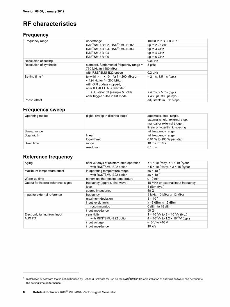
RF characteristics
Frequency underrange 100 kHz to < 300 kHz R&S®SMU-B102, R&S®SMU-B202 up to 2.2 GHz R&S®SMU-B103, R&S®SMU-B203 up to 3 GHz R&S®SMU-B104 up to 4 GHz
Frequency range
R&S®SMU-B106 up to 6 GHz Resolution of setting 0.01 Hz
standard, fundamental frequency range = 750 MHz to 1500 MHz
5 µHz Resolution of synthesis
with R&S®SMU-B22 option 0.2 µHz to within < 1 × 10⁻⁷ for f > 200 MHz or < 124 Hz for f < 200 MHz, with GUI update stopped, after IEC/IEEE bus delimiter
< 2 ms, 1.5 ms (typ.)
ALC state: off (sample & hold) < 4 ms, 2.5 ms (typ.)
Setting time 1
after trigger pulse in list mode < 450 µs, 300 µs (typ.) Phase offset adjustable in 0.1° steps
Frequency sweep Operating modes digital sweep in discrete steps automatic, step, single,
external single, external step, manual or external trigger, linear or logarithmic spacing
Sweep range full frequency range linear full frequency range Step width logarithmic 0.01 % to 100 % per step range 10 ms to 10 s Dwell time resolution 0.1 ms
Reference frequency after 30 days of uninterrupted operation < 1 × 10⁻⁹/day, < 1 × 10⁻⁷/year Aging
with R&S®SMU-B22 option < 5 × 10⁻¹⁰/day, < 3 × 10⁻⁸/year in operating temperature range ±6 × 10⁻⁸ Maximum temperature effect
with R&S®SMU-B22 option ±6 × 10⁻⁹ Warm-up time to nominal thermostat temperature ≤ 10 min
frequency (approx. sine wave) 10 MHz or external input frequency level 5 dBm (typ.)
Output for internal reference signal
source impedance 50 Ω frequency 5 MHz, 10 MHz or 13 MHz maximum deviation 3 × 10⁻⁶
input level, limits ≥ −6 dBm, ≤ 19 dBm recommended 0 dBm to 19 dBm
Input for external reference
input impedance 50 Ω sensitivity 1 × 10⁻⁸/V to 3 × 10⁻⁸/V (typ.)
with R&S®SMU-B22 option 4 × 10⁻⁹/V to 1.2 × 10⁻⁸/V (typ.) input voltage –10 V to +10 V
Electronic tuning from input AUX I/O
input impedance 10 kΩ
1 Installation of software that is not authorized by Rohde & Schwarz for use on the R&S®SMU200A or installation of antivirus software can deteriorate
the setting time performance.

Version 08.00, January 2012
Rohde & Schwarz R&S®SMU200A Vector Signal Generator 9
Level standard –145 dBm to +20 dBm Setting range with R&S®SMU-B31 or R&S®SMU-B36 option
to +30 dBm
standard f ≤ 3 GHz +13 dBm (PEP) 2 f > 3 GHz +11 dBm (PEP)
with R&S®SMU-B31 or R&S®SMU-B36 option
f ≤ 3 GHz +19 dBm (PEP)
Maximum level
f > 3 GHz +17 dBm (PEP) Resolution 0.01 dB
for levels > –120 dBm, attenuator mode: auto, temperature range = +18 °C to +28 °C
1 MHz ≤ f ≤ 3 GHz < 0.5 dB
Level uncertainty
f > 3 GHz < 0.9 dB Additional uncertainty with ALC state: off (sample & hold)
This function is needed only for some special applications.
< 0.2 dB
standard, ALC state: on f ≤ 3 GHz < 1.6, < 1.4 (typ.) f > 3 GHz < 1.85, < 1.6 (typ.)
with R&S®SMU-B31 or R&S®SMU-B36 option, ALC state: on
attenuator mode: normal f ≤ 3 GHz < 1.65, < 1.45 (typ.) f > 3 GHz < 1.9, < 1.65 (typ.)
attenuator mode: high power f ≤ 3 GHz < 1.7, < 1.5 (typ.)
Output impedance VSWR in 50 Ω system
f > 3 GHz < 1.9, < 1.65 (typ.) after IEC/IEEE bus delimiter, to < 0.1 dB deviation from final value, with GUI update stopped, temperature range = +18 °C to +28 °C
ALC state: on < 2 ms, 1.5 ms (typ.) ALC state: off < 4 ms, 2.5 ms (typ.)
in list mode after trigger impulse to 0.3 dB deviation from final value
< 450 µs, 300 µs (typ.)
Setting time 1
range switchover with R&S®SMU-B31 or R&S®SMU-B36 option
< 10 ms
attenuator mode: fixed, ALC state: on Uninterrupted level setting setting range > 20 dB
maximum permissible RF power in outputfrequency range for f > 1 MHz
1 MHz ≤ f ≤ 3 GHz 50 W f > 3 GHz 10 W
Back-feed (from ≥ 50 Ω source)
maximum permissible DC voltage 50 V
2 PEP = peak envelope power.

Version 08.00, January 2012
10 Rohde & Schwarz R&S®SMU200A Vector Signal Generator
Measured level data
0.5 1 1.5 2 2.5 3 3.5 4 4.5 5 5.5 6
x 109
10
12
14
16
18
20
22
24
26
28
30
RF frequency / Hz
Leve
l / d
Bm
Max. available output power with frequency option B106,Attenuator Mode Normal (lower trace) and High Power (upper trace)
0.5 1 1.5 2 2.5 3
x 109
10
12
14
16
18
20
22
24
26
28
30
RF frequency / Hz
Leve
l / d
Bm
Max. available output power with frequency option B103,Attenuator Mode Normal (lower trace) and High Power (upper trace)
Measured maximum available output level versus frequency.
Measured level uncertainty versus frequency.

Version 08.00, January 2012
Rohde & Schwarz R&S®SMU200A Vector Signal Generator 11
Measured level repeatability over 6 days with random settings between measurements (DACIF board temperature: internal temperature test point, variations caused by changes of ambient temperature).
Level sweep Operating modes digital sweep in discrete steps auto, single, step,
external single, external step, manual or external trigger
Sweep range level range of attenuator modes normal or high power
Step width logarithmic 0.1 dB to 20 dB per step range 10 ms to 10 s Dwell time resolution 0.1 ms

Version 08.00, January 2012
12 Rohde & Schwarz R&S®SMU200A Vector Signal Generator
Spectral purity standard, unmodulated
level < 8 dBm < –30 dBc level < 13 dBm < –30 dBc (typ.)
Harmonics
with R&S®SMU-B31 or R&S®SMU-B36 option, level < 12 dBm
< –30 dBc
level > –50 dBm, CW, vector modulation (full-scale DC input), > 10 kHz offset from carrier and outside the modulation spectrum
0.3 MHz ≤ f ≤ 200 MHz < –77 dBc 200 MHz < f ≤ 1500 MHz < –80 dBc 1500 MHz < f ≤ 3000 MHz < –74 dBc f > 3000 MHz < –68 dBc
> 850 kHz offset from carrier and outside the modulation spectrum 0.3 MHz ≤ f ≤ 200 MHz < –77 dBc 200 MHz < f ≤ 1500 MHz < –86 dBc 1500 MHz < f ≤ 3000 MHz < –80 dBc
Nonharmonics
f > 3000 MHz < –74 dBc level > –50 dBm, CW, vector modulation (full-scale DC input), > 10 kHz offset from carrier and outside the modulation spectrum
0.3 MHz ≤ f ≤ 200 MHz < –77 dBc (–87 dBc (typ.)) 200 MHz < f ≤ 1500 MHz < –90 dBc 1500 MHz < f ≤ 3000 MHz < –84 dBc
Nonharmonics with R&S®SMU-B22 option
f > 3000 MHz < –78 dBc Power supply and mechanically related nonharmonics
at RF = 1 GHz, 50 Hz to 10 kHz from carrier
< –70 dBc
1500 MHz < f ≤ 3000 MHz < –74 dBc Subharmonics f > 3000 MHz < –50 dBc > 10 MHz carrier offset, 1 Hz measurement bandwidth, CW
20 MHz ≤ f ≤ 200 MHz < –146 dBc (–149 dBc (typ.)) 200 MHz < f ≤ 1500 MHz < –150 dBc (–153 dBc (typ.)) 1.5 GHz < f ≤ 3 GHz < –148 dBc (–151 dBc (typ.)) f > 3 GHz < –146 dBc (–149 dBc (typ.))
vector modulation with full-scale DC input, 3 dB I/Q input gain 20 MHz ≤ f ≤ 200 MHz < –143 dBc (–146 dBc (typ.)) 200 MHz < f ≤ 1500 MHz < –146 dBc (–149 dBc (typ.)) 1.5 GHz < f ≤ 3 GHz < –145 dBc (–148 dBc (typ.))
Wideband noise
f > 3 GHz < –143 dBc (–146 dBc (typ.)) 20 kHz carrier offset, 1 Hz measurement bandwidth, CW
20 MHz ≤ f ≤ 200 MHz < –128 dBc (–132 dBc (typ.)) f = 1 GHz < –131 dBc (–135 dBc (typ.)) f = 2 GHz < –125 dBc (–129 dBc (typ.)) f = 3 GHz < –121 dBc (–125 dBc (typ.)) f = 4 GHz < –119 dBc (–123 dBc (typ.))
SSB phase noise
f = 6 GHz < –115 dBc (–119 dBc (typ.)) 20 kHz carrier offset, 1 Hz measurement bandwidth, CW
20 MHz ≤ f ≤ 200 MHz < –135 dBc (–138 dBc (typ.)) f = 1 GHz < –136 dBc (–139 dBc (typ.)) f = 2 GHz < –130 dBc (–133 dBc (typ.)) f = 3 GHz < –126 dBc (–129 dBc (typ.)) f = 4 GHz < –124 dBc (–127 dBc (typ.))
SSB phase noise with R&S®SMU-B22 option
f = 6 GHz < –120 dBc (–123 dBc (typ.)) RMS value at f = 1 GHz
300 Hz to 3 kHz < 1 Hz Residual FM
20 Hz to 23 kHz < 4 Hz Residual AM RMS value from 20 Hz to 23 kHz < 0.02 %
Version 08.00, January 2012
Rohde & Schwarz R&S®SMU200A Vector Signal Generator 13
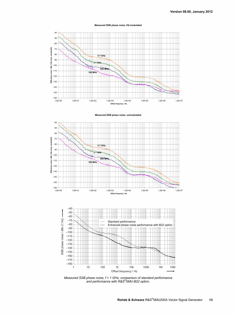
Measured SSB phase noise, I/Q modulated
-160
-150
-140
-130
-120
-110
-100
-90
-80
-70
-60
-50
-40
1,0E+00 1,0E+01 1,0E+02 1,0E+03 1,0E+04 1,0E+05 1,0E+06 1,0E+07
Offset frequency / Hz
SS
Bp
ha
se
no
ise
/d
Bc
(1H
zm
eas
.b
an
dw
idth
)
5.7 GHz
2.1 GHz
850 MHz
100 MHz
Measured SSB phase noise, unmodulated
-160
-150
-140
-130
-120
-110
-100
-90
-80
-70
-60
-50
-40
1,0E+00 1,0E+01 1,0E+02 1,0E+03 1,0E+04 1,0E+05 1,0E+06 1,0E+07
Offset frequency / Hz
SS
Bp
ha
se
no
ise
/d
Bc
(1H
zm
eas
.b
an
dw
idth
)
5.7 GHz
2.1 GHz
850 MHz
100 MHz
–180–170–160–150–140–130–120–110–100–90–80–70–60–50–40
1 10 100 1k 10k 100k 1M 10MOffset frequency / Hz
SSB
phas
e no
ise
/ dBc
(1 H
z)
Standard performance Enhanced phase noise performance with B22 option
Measured SSB phase noise, f = 1 GHz, comparison of standard performance and performance with R&S®SMU-B22 option.

Version 08.00, January 2012
14 Rohde & Schwarz R&S®SMU200A Vector Signal Generator
List mode Frequency and level values can be stored in a list and set in an extremely short amount of time. Operating modes automatic, single sweep, manual or
external trigger, fast hopping with immediate and external trigger
Max. number of channels 10000 Dwell time 1 ms to 1 s
Resolution 0.1 ms after external trigger see frequency and level data Setting time additional trigger delay in two-path units, both paths operated in list mode
< 200 µs
Phase coherence (R&S®SMU-B90 option) The R&S®SMU-B90 provides phase-coherent RF outputs of two or more RF paths for one or more instruments with I/Q modulation.
The R&S®SMU-B90 option can be installed in any R&S®SMU200A with serial number 103001 or higher.
internal This mode corresponds to normal operation. Each RF path uses its internal local oscillator.
external An external signal is used for path A. With a two-path instrument, the internal local oscillator signal is used for path B.
coupled A –> B The local oscillator signal of path A is also used for path B (only for two-path instruments).
Coupling modes
externally coupled A –> B An external signal is input at the LO IN connector and used for the coupled paths A and B (only for two-path instruments).
The internal local oscillator signal used with path A is also available on the LO OUT connector (in order to couple two instruments).
on LO out state
The LO OUT signal is switched off. off internal mode (no LO coupling)
underrange 100 kHz to < 300 kHz R&S®SMU-B102, R&S®SMU-B202
up to 2 GHz
R&S®SMU-B103, R&S®SMU-B203,
up to 3 GHz
R&S®SMU-B104 up to 4 GHz
Frequency range
R&S®SMU-B106 up to 6 GHz external modes, coupled A –> B, externally coupled A –> B
R&S© SMU-B102 and R&S© SMU-B202
200 MHz to 2 GHz
R&S© SMU-B103 and R&S© SMU-B203
200 MHz to 3 GHz
other configurations Coupling is possible within the smallest common frequency range of all RF paths to be coupled.
LO IN 10 dBm to 16 dBm (nom.) Levels of external local oscillator signals LO OUT 13 dBm (nom.)

Version 08.00, January 2012
Rohde & Schwarz R&S®SMU200A Vector Signal Generator 15
drift versus temperature 0.1° (nom.)
when ambient temperature changes by 1 °C
versus time 0.02°/h (nom.)
versus level 2°/dB (nom.)
setting range (with baseband phase offset)
0.00° to 359.99°
Phase
setting resolution 0.01°

Version 08.00, January 2012
16 Rohde & Schwarz R&S®SMU200A Vector Signal Generator
Analog modulation
Internal modulation generator Frequency range 0.1 Hz to 1 MHz Resolution of setting 0.1 Hz Frequency uncertainty < 0.012 Hz +
relative deviation of reference frequency up to 100 kHz < 0.1 dB Frequency response up to 1 MHz < 1 dB
Distortion up to 100 kHz at RL > 200 Ω, level = 1 V (Vp)
< 0.1 %
Vp at LF connector, RL > 200 Ω 1 mV to 3 V resolution 1 mV
Output voltage
setting uncertainty at 1 kHz < (1 % of reading + 1 mV) Output impedance 16 Ω Frequency setting time to within < 1 × 10⁻⁷, with GUI update
stopped, after IEC/IEEE bus delimiter < 3 ms
digital sweep in discrete steps operating modes
automatic, step, single, external single, external step, manual or external trigger, linear or logarithmic spacing
sweep range entire frequency range linear step width entire frequency range
Sweep
logarithmic step width 0.01 % to 100 % per step
Input for external modulation signals input impedance
high (> 100 kΩ), switchable to 50 Ω with R&S®SMU-B20 or R&S®SMU-B22 option
input sensitivity (peak value for set modulation depth or deviation)
1 V
Modulation input EXT MOD
maximum permissible input voltage ±10 V
Amplitude modulation Operating modes internal, external AC/DC Modulation depth modulation is clipped at high levels if
maximum PEP is reached 0 % to 100 %
Resolution 0.1 % Setting uncertainty attenuator mode: auto,
fmod = 1 kHz and m < 80 % < (1 % of reading + 1 %)
PEP in specified range, attenuator mode: auto f ≤ 3 GHz, at fmod = 1 kHz, m = 30 % < 0.5 % m = 80 % < 0.8 % f > 3 GHz, at fmod = 1 kHz, m = 30 % < 1 %
AM distortion
m = 80 % < 1.6 % Modulation frequency range DC, 20 Hz to 500 kHz Modulation frequency response AC mode, 20 Hz to 500 kHz < 1 dB Synchronous φM at AM m = 30 %, fmod = 1 kHz, peak value < 0.1 rad
Wideband amplitude modulation Operating modes modulation input I external DC Modulation frequency response as with I/Q modulation – external wideband I/Q Input impedance 50 Ω Input sensitivity peak voltage for 100 % AM 0.25 V

Version 08.00, January 2012
Rohde & Schwarz R&S®SMU200A Vector Signal Generator 17
Pulse modulation Operating modes external,
internal (duty cycle approx. 1:1) On/off ratio > 70 dB Rise/fall time 10 %/90 % of RF amplitude 1 µs (typ.) Pulse repetition frequency 0 Hz to 100 kHz Video crosstalk spectral line of fundamental of 100 kHz
square-wave modulation < −30 dBc
input level rising 1.7 V, falling 1.1 V (typ.) input impedance > 10 kΩ
Modulation input EXT MOD A/B
polarity selectable
Frequency modulation (R&S®SMU-B20 or R&S®SMU-B22 option) Operating modes internal, external, internal + external,
AC/DC, normal, low noise (with R&S®SMU-B22 only)
0.3 MHz ≤ f ≤ 200 MHz rm = 1 200 MHz < f ≤ 375 MHz rm = 0.25 375 MHz < f ≤ 750 MHz rm = 0.5 750 MHz < f ≤ 1500 MHz rm = 1 1500 MHz < f ≤ 3000 MHz rm = 2
FM/φM range multiplier
f > 3000 MHz rm = 4 FM mode: normal rm × 10 MHz Maximum deviation FM mode: low noise rm × 100 kHz
Resolution < 200 ppm, min. rm × 0.1 Hz fmod = 10 kHz, deviation ≤ half of maximum deviation
internal < (1.5 % of reading + 20 Hz) Setting uncertainty
external < (2.0 % of reading + 20 Hz) FM distortion fmod = 10 kHz and 1 MHz deviation < 0.1 %
FM mode: normal 10 Hz to 100 kHz < 0.5 dB 10 Hz to 10 MHz < 3 dB
FM mode: low noise
Modulation frequency response
10 Hz to 100 kHz < 3 dB 40 kHz deviation, fmod = 1 kHz, f > 5 MHz < 0.1 % Synchronous AM f > 3 GHz < 0.2 %
Carrier frequency offset at FM < 0.2 % of set deviation
Phase modulation (R&S®SMU-B20 or R&S®SMU-B22 option) Operating mode internal, external, internal + external,
AC/DC, high bandwidth, high deviation, low noise (with R&S®SMU-B22 only)
φM mode: high deviation rm × 20.0 rad φM mode: high bandwidth rm × 1.0 rad
Maximum deviation
φM mode: low noise rm × 0.25 rad φM mode: high deviation < 200 ppm, min. rm × 20 µrad φM mode: high bandwidth < 0.1 %, min. rm × 20 µrad
Resolution
φM mode: low noise < 200 ppm, min. rm × 20 µrad fmod = 10 kHz, deviation ≤ half of maximum deviation
internal < (1.5 % of reading + 0.01 rad) Setting uncertainty
external < (2.0 % of reading + 0.01 rad) φM distortion fmod = 10 kHz, half of maximum deviation < 0.2 %, 0.1 % (typ.)
10 Hz to 500 kHz, φM mode: high deviation
< 1 dB
10 Hz to 10 MHz, φM mode: high bandwidth
< 3 dB
Modulation frequency response
10 Hz to 100 kHz, φM mode: low noise < 3 dB

Version 08.00, January 2012
18 Rohde & Schwarz R&S®SMU200A Vector Signal Generator
I/Q modulation
I/Q modulator Operating modes external wideband I/Q,
internal baseband I/Q I offset, Q offset
setting range −10 % to +10 % resolution 0.01 %
gain imbalance setting range −1.0 dB to +1.0 dB resolution 0.001 dB
quadrature offset setting range −10° to +10°
I/Q impairments
resolution 0.01° I/Q swap I and Q signals swapped on/off
External wideband I/Q This type of modulation is possible only in path A.
input impedance 50 Ω VSWR up to 50 MHz < 1.2 input voltage for full-scale input
q2 2i + = 0.5 VV V
I/Q inputs
minimum input voltage for ALC state: on 0.1 V Modulation frequency range I/Q wideband: on 100 MHz
I/Q wideband: on up to 50 MHz < 6 dB (typ.)
RF frequency response for entire instrument in modulation bandwidth
up to 5 MHz < 1.0 dB (typ.) Carrier leakage without input signal, referenced to
full-scale input 3 < −55 dBc, < −65 dBc (typ.)
measured with 16QAM, root cosine filter, α = 0.5, symbol rate 10 kHz RMS value
f ≤ 200 MHz < 0.3 % f > 200 MHz < (0.2 % + 0.1 % × f/GHz)
peak value f ≤ 200 MHz < 0.6 %
Error vector
f > 200 MHz < (0.4 % + 0.2 % × f/GHz)
De
lta /
dB
5
4
3
2
1
0
–1
– 2
– 3
– 4
– 5
Frequency offset from carrier / MHz
– 100 1000 60– 20– 60 20 40 80– 80 – 40
RF 850 MHzRF 1900 MHzRF 2200 MHz
Measured frequency response of external wideband I/Q modulation.
3 Value applies after 1 hour warm-up time and recalibration for 4 hours of operation and temperature variations of less than +5 °C.

Version 08.00, January 2012
Rohde & Schwarz R&S®SMU200A Vector Signal Generator 19
Internal baseband I/Q (with R&S®SMU-B13 option) The R&S®SMU-B13 option converts the internal digital baseband signals of the R&S®SMU-B9/-B10/-B11 into analog signals for driving the I/Q modulator. It also generates the analog I/Q output signals. One or two R&S®SMU-B13 can be installed. The first R&S®SMU-B13 drives RF path A, the second RF path B. The I/Q output signals are available either for path A or B.
data rate 100 MHz resolution 16 bit
D/A converter
sample rate 400 MHz (internal interpolation × 4) with amplitude, group delay and Si correction
bandwidth, roll-off to −0.1 dB 40 MHz D/A converter interpolation spectra
up to 10 MHz < −80 dBc
Aliasing filter
up to 40 MHz < −73 dBc carrier leakage
setting range −10 % to +10 % resolution 0.01 %
I ≠ Q (imbalance) setting range −1 dB to +1 dB resolution 0.001 dB
quadrature offset setting range −10° to +10°
I/Q impairment
resolution 0.01° f > 100 MHz, –20 dBm ≤ level ≤ 10 dBm, I/Q wideband: on, optimize internal I/Q impairments for RF output: on, optimization mode: high quality
up to 10 MHz < 0.5 dB, 0.1 dB (typ.)
RF frequency response for entire instrument in modulation bandwidth
up to 40 MHz < 2.0 dB, 0.3 dB (typ.) up to 10 MHz > 50 dB, 56 dB (typ.) Suppression of image sideband for entire
instrument in modulation bandwidth 3 up to 40 MHz > 40 dB, 50 dB (typ.) Carrier leakage 3 referenced to full-scale input < −55 dBc, < −65 dBc (typ.) Additional level uncertainty referenced to CW
measured at 0 dBm with 16QAM, root cosine filter, α = 0.5, 10 kHz symbol rate
< 0.2 dB
I/Q outputs Output impedance 50 Ω Output voltage EMF (output voltage depends on set
modulation signal) 1 V (Vp)
Offset EMF < 1 mV at RL = 50 Ω magnitude
up to 10 MHz 0.02 dB (typ.) up to 40 MHz 0.03 dB (typ.)
nonlinear phase up to 10 MHz 0.1° (typ.)
Frequency response 4
up to 30 MHz 0.2° (typ.) at RL = 50 Ω magnitude
up to 10 MHz 0.01 dB (typ.) up to 40 MHz 0.02 dB (typ.)
nonlinear phase up to 10 MHz 0.1° (typ.)
I/Q balance 4
up to 30 MHz 0.2° (typ.) at RL = 50 Ω SFDR (sine)
up to 2 MHz > 70 dB up to 20 MHz 60 dB (typ.)
phase noise 10 MHz sine wave at 20 kHz offset −150 dBc (typ.)
wideband noise
Spectral purity
10 MHz sine wave at 1 MHz offset −155 dBc (typ.)
4 Optimize internal I/Q impairments for RF output switched off.

Version 08.00, January 2012
20 Rohde & Schwarz R&S®SMU200A Vector Signal Generator
Measured frequency response of I/Q outputs.
Measured SFDR of I/Q outputs.

Version 08.00, January 2012
Rohde & Schwarz R&S®SMU200A Vector Signal Generator 21
Differential I/Q output (R&S®SMU-B16 option) One R&S®SMU-B16 option can be installed; the I/Q output signals are available either for path A or B. This option is not compatible with rear-panel outputs (R&S®SMU-B81 and R&S®SMU-B82 options).
Additional specifications for I/Q outputs with R&S®SMU-B16 option Output impedance
Single-ended 50 Ω Differential 100 Ω
Output voltage output voltage depends on set modulation signal Single-ended EMF 0.02 V to 2 V (Vp)
Resolution 1 mV Differential EMF 0.04 V to 4 V (Vpp)
Resolution 2 mV Bias voltage (single-ended and differential) EMF –3.6 V to +3.6 V
Resolution 2 mV Uncertainty 1 % + 4 mV
Offset voltage Differential EMF –300 mV to +300 mV
Resolution 0.2 mV Uncertainty 1 % + 0.1 % × bias voltage + 1 mV
at RL = 50 Ω, output voltage > 0.5 V (Vp) magnitude
up to 10 MHz < 0.2 dB, 0.05 dB (typ.)
Differential signal balance
up to 40 MHz 0.2 dB (typ.) at RL = 50 Ω, output voltage > 0.5 V (Vp) magnitude
up to 10 MHz 0.02 dB (typ.) up to 40 MHz 0.03 dB (typ.)
nonlinear phase up to 10 MHz 0.1° (typ.)
Frequency response 5
up to 30 MHz 0.2° (typ.)
Digital baseband output (R&S®SMU-B18 option) The R&S®SMU-B18 option makes digital I/Q signals available on the rear panel of the instrument. The digital I/Q output can be used for the lossless connection of the R&S®SMU200A to the digital I/Q input of other Rohde & Schwarz instruments (e.g. R&S®AMU200A baseband signal generator and fading simulator). One R&S®SMU-B18 can be installed.
standard
in line with Rohde & Schwarz TVR290, I/Q data and control signals, data and interface clock
level LVDS connector 26-pin MDR
Interface
data rate 30 MHz to 100 MHz with 1 MHz resolution, 81.6 MHz
With source ‘user-defined’, the sample rate must be entered via the parameter ‘sample rate’, no I/Q data clock being necessary. With source ‘digital I/Q out’ or ‘digital I/Q in’, the sample rate will be estimated on the basis of the applied I/Q data clock. source user-defined, digital I/Q out, digital I/Q in sample rate 400 Hz to 100 MHz max. sample rate limited by actual
interface data rate resolution (user-defined) 0.001 Hz
I/Q sample rate
frequency uncertainty (user-defined) < 5 × 10⁻¹⁴
5 Optimize internal I/Q impairments for RF output switched off.

Version 08.00, January 2012
22 Rohde & Schwarz R&S®SMU200A Vector Signal Generator
resolution 18 bit logic format two’s complement physical signal level
setting range 0 to –60 dBFS resolution 0.01 dBFS
bandwidth sample rate = 100 MHz (no interpolation, user-defined)
40 MHz
I/Q data
sample rate < 100 MHz (interpolation) 0.31 × sample rate markers 4 Control signals data valid valid samples marked in data stream
Baseband input (analog/digital) (R&S®SMU-B17 option) At least one R&S®SMU-B13 baseband main module and at least one R&S®SMU-B9/-B10/-B11 I/Q baseband generator must be installed. The R&S®SMU-B17 option makes it possible to feed external analog or digital signals to the baseband section of the R&S®SMU200A. The frequency of the signals can be shifted, and the signals can be added to the internally generated signal with settable level ratio. If the R&S®SMU200A is equipped with a fading simulator, the input signals can also be faded.
Mode see also simultaneous modulation analog input, digital input
peak level setting range –10 dB to 0 dB referenced to full scale resolution 0.01 dB
crest factor setting range 0 dB to 30 dB resolution 0.01 dB
Input level
The adjust level function automatically determines the peak level and crest factor of the input signal. The frequency offset can be used to shift the center frequency of the input signal in the baseband. The restrictions caused by the modulation bandwidth apply. setting range −40 MHz to +40 MHz resolution 0.01 Hz
Frequency offset
frequency accuracy < 5 × 10 − 10 × frequency offset + reference frequency error
I/Q swap I and Q signals swapped on/off Analog I/Q inputs All specifications apply to a peak level of 0 dB.
input impedance 50 Ω VSWR up to 30 MHz < 1.1, 1.03 (typ.)
I/Q inputs
input voltage for full-scale input q
2 2i + = 0.5 VV V
carrier leakage I, Q setting range −10 % to +10 % resolution 0.01 %
I ≠ Q (imbalance) setting range −3 dB to +3 dB resolution 0.001 dB
I/Q skew setting range –1 ns to +1 ns
I/Q impairment
resolution 1 ps sample rate 100 MHz A/D converter resolution 14 bit with amplitude and group delay correction bandwidth, roll-off to –0.1 dB 30 MHz
Aliasing filter
stopband rejection, f ≥ 70 MHz 80 dB (typ.) I/Q wideband: on, optimize internal I/Q impairments for RF output: on
up to 10 MHz 0.2 dB (typ.) RF frequency response for entire instrument in modulation bandwidth
up to 30 MHz 0.4 dB (typ.)

Version 08.00, January 2012
Rohde & Schwarz R&S®SMU200A Vector Signal Generator 23
Carrier leakage referenced to full scale < −55 dBc, < −65 dBc (typ.) up to 10 MHz 56 dB (typ.) Suppression of image sideband for entire
instrument in modulation bandwidth up to 30 MHz 50 dB (typ.) wideband noise, with full-scale DC input
20 MHz ≤ f ≤ 200 MHz –145 dBc (typ.) 200 MHz < f ≤ 1.5 GHz –148 dBc (typ.) 1.5 GHz < f ≤ 3 GHz –148 dBc (typ.) f > 1.5 GHz –145 dBc (typ.)
ACLR with an ideal input signal, 3GPP test model 1, 64 DPCH level ≤ 10.5 dBm PEP, ≤ 16.5 dBm PEP with R&S®SMU-B31, R&S®SMU-B36 options frequency = 1800 MHz to 2200 MHz
5 MHz offset (baseband gain: 3 dB) 70 dB (typ.)
RF spectral purity
10 MHz offset (baseband gain: 6 dB) 73 dB (typ.) Digital I/Q inputs
standard in line with Rohde & Schwarz TVR290, I/Q data and control signals, data and interface clock
level LVDS connector 26-pin MDR
Interface
data rate 66 MHz to 100 MHz source user-defined, digital I/Q in sample rate 400 Hz to 100 MHz
resolution (user-defined) 0.001 Hz
I/Q sample rate (max. sample rate depends on interface data rate) With source ‘user-defined’, the sample rate must be entered via the parameter ‘sample rate’, no I/Q data clock being necessary. With source ‘digital I/Q in’, the sample rate will be estimated on the basis of the applied I/Q data clock.
frequency uncertainty (user-defined) < 5 × 10⁻¹⁴
resolution 18 bit logic format two’s complement bandwidth
sample rate = 100 MHz (no interpolation, user-defined)
40 MHz
I/Q data
sample rate < 100 MHz (interpolation) 0.31 × sample rate markers 4 Control signals data valid valid samples marked in data stream

Version 08.00, January 2012
24 Rohde & Schwarz R&S®SMU200A Vector Signal Generator
I/Q baseband generator (R&S®SMU-B9/-B10/-B11 option) – arbitrary waveform mode At least one R&S®SMU-B13 baseband main module must be installed. One or two R&S®SMU-B9/-B10/-B11 options can be installed. Their I/Q signals can be assigned a frequency offset and/or be added in the digital domain with settable level ratio.
output memory waveform length with R&S®SMU-B9 option
128 sample to 128 Msample in one-sample steps
waveform length with R&S®SMU-B10 option
128 sample to 64 Msample in one-sample steps
waveform length with R&S®SMU-B11 option
128 sample to 16 Msample in one-sample steps
resolution 16 bit loading time 10 Msample 15 s
Waveform memory
nonvolatile memory hard disk number of segments max. 1024 segments changeover modes GUI, remote control, external trigger extended trigger modes same segment, next segment, next
segment seamless, sequencer changeover time at 50 MHz clock rate (external trigger, without clock change)
5 µs (meas.)
seamless changeover output up to end of current segment, followed by changeover to next segment
sequencer play list length max. 96
Multisegment waveform
sequencer segment repetitions max. 65535 number of carriers max. 32 total RF bandwidth max. 80 MHz crest factor modes maximize, minimize, off signal period modes longest file, shortest file, user (max. 1 s) single carrier gain –80 dB to 0 dB single carrier start phase 0° to 360°
Multicarrier waveform
single carrier delay 0 s to 1 s clock rate 400 Hz to 100 MHz resolution 0.001 Hz operating mode internal, external
Clock generation
frequency uncertainty (internal) < 5 × 10⁻¹⁴ × clock rate + uncertainty of reference frequency
The sample rate of the waveform is automatically interpolated to the internal 100 MHz data rate. bandwidth
clock rate = 100 MHz (no interpolation), roll-off to –0.1 dB
40 MHz
Interpolation
clock rate ≤ 100 MHz, drop to −0.1 dB 0.31 × clock rate The frequency offset can be used to shift the center frequency of the wanted baseband signal. The restrictions caused by the modulation bandwidth apply. range −40 MHz to +40 MHz resolution 0.01 Hz
Frequency offset
frequency uncertainty < 5 × 10 − 10 × frequency offset + reference frequency error

Version 08.00, January 2012
Rohde & Schwarz R&S®SMU200A Vector Signal Generator 25
In internal clock mode, a trigger event restarts the clock generation. The clock phase is then synchronous with the trigger (with a certain timing uncertainty). In external clock mode, the trigger event is synchronized to the symbol clock. operating mode internal, external modes auto, retrig, armed auto, armed retrig setting uncertainty for clock phase related to trigger in internal clock mode
< 18 ns
external trigger delay setting range 0 sample to (216 – 1) sample
resolution internal clock mode 0.01 sample external clock mode 1 sample setting uncertainty < 5 ns
external trigger inhibit setting range 0 sample to (226 – 1) sample resolution 1 sample
external trigger pulse width > 15 ns
Triggering
external trigger frequency < 0.02 × sample rate number 4 level LVTTL operating modes unchanged, restart, pulse, pattern, ratio marker delay
setting range 0 sample to (waveform length − 1) sample setting range without recalculation 0 sample to 2000 sample resolution of setting 0.001 sample
Marker outputs
setting uncertainty < 10 ns Operation with R&S®WinIQSIM2™: As of version 1.00, the software supports I/Q data download and control of the R&S®SMU-B9/-B10/-B11 options.
Version 08.00, January 2012
26 Rohde & Schwarz R&S®SMU200A Vector Signal Generator
I/Q baseband generator (R&S®SMU-B9/-B10/-B11 option) – realtime operation At least one R&S®SMU-B13 baseband main module must be installed. One or two R&S®SMU-B9/-B10/-B11 options can be installed. Their I/Q signals can be assigned a frequency offset and/or be added in the digital domain with settable level ratio.
ASK modulation index 0 % to 100 % resolution 0.1 %
FSK 2FSK, 4FSK, MSK deviation 0.1 to 1.5 × fsym
maximum 10 MHz resolution < 0.1 Hz setting uncertainty < 0.5 %
variable FSK 4FSK, 8FSK, 16FSK deviations –1.5 × fsym to +1.5 × fsym
maximum 10 MHz resolution < 0.1 Hz
PSK BPSK, QPSK, QPSK 45° offset, OQPSK, π/4-QPSK, π/2-DBPSK, π/4-DQPSK, π/8-D8PSK, 8PSK, 8PSK EDGE
Types of modulation
QAM 16QAM, 32QAM, 64QAM, 256QAM, 1024QAM
Coding Not all coding methods can be used with every type of modulation.
off, differential, diff. phase, diff. + Gray, Gray, GSM, NADC, PDC, PHS, TETRA, APCO25 (PSK), PWT, TFTS, INMARSAT, VDL, EDGE, APCO25(FSK), ICO, CDMA2000® 6, WCDMA
Any filter can be used with any type of modulation. The bandwidth of the modulation signal is max. 25 MHz; the signal is clipped if the bandwidth is exceeded. cosine, root cosine
filter parameter α 0.05 to 1.00 Gaussian
filter parameter B × T 0.15 to 2.50 cdmaOne, cdmaOne + equalizer cdmaOne 705 kHz, cdmaOne 705 kHz + equalizer CDMA2000® 3x APCO25 C4FM rectangular split phase
filter parameter B × T 0.15 to 2.5
Baseband filter
resolution of filter parameter 0.01 If an external clock is used, the applied data rate may deviate from the set clock rate by ±2 %. The external clock can be used for internal and external data. operating mode internal, external setting range
ASK, PSK, QAM 400 Hz to 25 MHz FSK 400 Hz to 15 MHz
resolution 0.001 Hz frequency uncertainty (internal)
< 5 × 10–14 × symbol rate + reference frequency uncertainty
external clock symbol, K × symbol, bit clock clock divider K 1 to 64
Symbol rate
external clock rate max. 100 MHz
6 CDMA2000® is a registered trademark of the Telecommunications Industry Association (TIA - USA).

Version 08.00, January 2012
Rohde & Schwarz R&S®SMU200A Vector Signal Generator 27
The frequency offset can be used to shift the center frequency of the modulation signal in the baseband. The restrictions caused by the modulation bandwidth apply. setting range −40 MHz to +40 MHz resolution 0.01 Hz
Frequency offset
frequency uncertainty < 5 × 10 − 10 × frequency offset + reference frequency error
internal All 0, All 1 PRBS
sequence length 9, 11, 15, 16, 20, 21, 23 pattern
length 1 bit to 64 bit data lists
R&S®SMU-B9 output memory 8 bit to 4 Gbit R&S®SMU-B10 output memory 8 bit to 2 Gbit R&S®SMU-B11 output memory 8 bit to 512 Mbit nonvolatile memory hard disk
external In the case of serial transmission, the symbol strobe marks the LSB of the symbol, and the maximum symbol rate is limited by the data rate of the interface. serial
word width 1 bit to 10 bit bit rate max. 60 MHz
parallel word width 1 bit to 10 bit
Data sources
symbol rate max. 25 MHz In internal clock mode, a trigger event restarts the clock generation. The clock phase is then synchronous with the trigger (with a certain timing uncertainty). In external clock mode, the trigger event is synchronized to the symbol clock. operating mode internal, external modes auto, retrig, armed auto, armed retrig setting uncertainty for clock phase related to trigger in internal clock mode
< 18 ns
external trigger delay setting range 0 sample to (216 – 1) sample
resolution internal clock mode 0.01 sample external clock mode 1 sample setting uncertainty < 5 ns
external trigger inhibit setting range 0 sample to (226 – 1) sample resolution 1 sample
external trigger pulse width > 15 ns
Triggering
external trigger frequency < 0.02 × sample rate

Version 08.00, January 2012
28 Rohde & Schwarz R&S®SMU200A Vector Signal Generator
number 4 level LVTTL operating modes control list, restart, pulse, pattern, ratio marker delay (in sample)
setting range 0 to 224 – 1 setting range without recalculation 0 to 2000 resolution of setting 0.001
Marker outputs
setting uncertainty < 10 ns Internal or external via LEVATT input. The signal switches between nominal and reduced level (without edge shaping). If an internal LEVATT signal is used, the connector is used as an output. setting range 0 dB to 60 dB additional level error in case of reduction
up to 30 dB < 1 dB
Level reduction
up to 50 dB < 3 dB Internal or external via BURST input. The signal triggers the beginning of a power ramp. The positive edge starts power ramping from blank to full level, the negative edge ramping in the opposite direction from full level to blanking. If an internal BURST GATE signal is applied, the connector is used as an output. operating range max. 5 MHz rise/fall time
setting range 0.5 symbol to 16 symbol resolution 0.1 symbol
Burst
ramp shape cosine, linear The input impedance and trigger threshold can be set separately for the trigger and the clock/data inputs. input impedance 1 kΩ, 50 Ω trigger threshold
setting range 0.00 V to 2.50 V
Trigger/clock/data inputs
resolution 0.01 V Clock/data outputs level LVTTL

Version 08.00, January 2012
Rohde & Schwarz R&S®SMU200A Vector Signal Generator 29
modulation, filter, symbol rate and coding in line with standard Predefined settings standards Bluetooth® 7, DECT, ETC, GSM,
GSM EDGE, NADC, PDC, PHS, TETRA, WCDMA 3GPP, TD-SCDMA, CDMA2000® Forward, CDMA2000® Reverse, Worldspace
Modulation errors deviation 0.2 to 0.7 × symbol rate Gaussian filter with B × T = 0.2 to 0.7
symbol rate up to 2 MHz < 1.2 %, 0.25 % (typ.)
Deviation error with 2FSK, 4FSK
symbol rate up to 10 MHz 0.75 % (typ.) Gaussian filter with B × T = 0.2 to 0.7
bit rate up to 2 MHz < 0.4°, 0.15° (typ.) Phase error with MSK
bit rate up to 10 MHz 0.3° (typ.) cosine, root cosine filter with α = 0.2 to 0.7
symbol rate up to 5 MHz < 0.8 %, 0.2 % (typ.) EVM with QPSK, OQPSK, π/4-DQPSK, 8PSK, 16QAM, 32QAM, 64QAM
symbol rate up to 20 MHz 0.7 % (typ.)
Measured EVM versus symbol rate.
7 The Bluetooth® word mark and logos are registered trademarks owned by Bluetooth SIG, Inc. and any use of such marks by Rohde & Schwarz is
under license.

Version 08.00, January 2012
30 Rohde & Schwarz R&S®SMU200A Vector Signal Generator
Modulation uncertainty for main standards Typical values
Standard GSM EDGE WCDMA 3GPP (1DPCH)
cdmaOne Reverse
DECT TETRA NADC PDC IEEE 802.11a
800 to 900 824 to 894 810 to 956 2400 to 2485
Frequency in MHz
400 to 2000
400 to 2000
1800 to 2200
1850 to 2000
1880 to 1990
380 to 480
1850 to 2000
1429 to 1501
5150 to 5825
EVM in % – 0.2 0.3 0.2 – 0.2 0.2 0.2 0.4 Phase error in °
0.15 – – – – – – – –
Deviation error in kHz
– – – – 0.5 – – – –
Channel spacing
200 kHz 200 kHz 5 MHz 1.25 MHz 1.728 MHz 25 kHz 30 kHz 25 kHz –
Adjacent channel power ratio (ACPR) in dB 8 In adjacent channel
−37 −38 −72 9 −85 10 – −74 11 −34 −74 −42 at 11 MHz
In alternate channel
−71 −71 −78 12 −89 13 – −77 11 −80 −82 −64 at 20 MHz
In 2nd alternate channel
−85 −85 – −9514 – – – – −66 at 30 MHz
Signal performance for digital standards GSM/EDGE with R&S®SMU-K40 option Burst on/off ratio > 100 dB
MSK, Gaussian filter B × T = 0.3 RMS < 0.4°, 0.15° (typ.)
Phase error
peak < 1.2°, 0.4° (typ.) Error vector magnitude 8PSK EDGE, Gaussian linearized filter,
RMS < 0.5 %, 0.2 % (typ.)
values measured with 30 kHz resolution bandwidth, referenced to level in band center without power ramping level ≤ 10.5 dBm, ≤ 16.5 dBm with R&S®SMU-B31, R&S®SMU-B36 options
200 kHz offset < –34 dB, –37 dB (typ.) 400 kHz offset < –68 dB, –71 dB (typ.)
Power density spectrum
600 kHz offset < –80 dB, –85 dB (typ.)
8 Level restricted, see specifications. 9 0 dB baseband gain (standard). 10 885 kHz offset and 30 kHz bandwidth. 11 Measured with root cosine filter. 12 6 dB baseband gain (low noise). 13 1.25 MHz offset and 30 kHz bandwidth. 14 1.98 MHz offset and 30 kHz bandwidth.

Version 08.00, January 2012
Rohde & Schwarz R&S®SMU200A Vector Signal Generator 31
3GPP FDD with R&S®SMU-K42 option Error vector magnitude 1 DPCH, RMS < 0.8 %, 0.3 % (typ.)
test model 1, 64 DPCH level ≤ 10.5 dBm PEP, ≤ 16.5 dBm PEP with R&S®SMU-B31, R&S®SMU-B36 options frequency = 1800 MHz to 2200 MHz
5 MHz offset (baseband gain: 3 dB) > 67 dB, 71 dB (typ.)
Adjacent channel leakage ratio (ACLR)
10 MHz offset (baseband gain: 6 dB) > 72 dB, 74 dB (typ.)
A
Ref -9.1 dBm
*
*
*1 RM
CLRWR
3DB
RBW 30 kHz
VBW 300 kHz
SWT 2 sAtt 10 dB*
NOR
*
Center 2.14 GHz Span 25.5 MHz2.55 MHz/
-100
-90
-80
-70
-60
-50
-40
-30
-20-10
Tx Channel W-CDMA 3GPP FWD
Bandwidth 3.84 MHz Power -6.67 dBm
Adjacent Channel
Bandwidth 3.84 MHz Lower -72.03 dB Spacing 5 MHz Upper -72.46 dB
Alternate Channel
Bandwidth 3.84 MHz Lower -74.10 dB Spacing 10 MHz Upper -74.06 dB
1
Marker 1 [T1 ]
-26.78 dBm
2.138447115 GHz
↑POS -9.079 dBm
Measured ACPR for 3GPP test model 1, 64 DPCH (baseband gain: +3 dB).
A
Ref -16.7 dBm
*
*
*
CLRWR
3DB
RBW 30 kHz
VBW 300 kHz
1 RM
SWT 2 sAtt 10 dB*
NOR
*
Center 2.14 GHz Span 40.6 MHz4.06 MHz/
-110
-100
-90
-80
-70
-60
-50
-40
-30
-20
Standard: W-CDMA 3GPP FWD
Tx Channels
Ch1 -12.73 dBm(Ref)
Ch2 -12.77 dBm
Ch3 -12.71 dBm
Ch4 -12.70 dBm
Total -6.70 dBm
Adjacent Channel
Lower -65.70 dB
Upper -65.22 dB
Alternate Channel
Lower -66.15 dB
Upper -66.12 dB
1
Marker 1 [T1 ]
-33.39 dBm
2.138447115 GHz
↑POS -16.66 dBm
Measured ACPR for a 3GPP four-carrier signal with test model 1, 64 DPCH on each carrier (baseband gain: +3 dB).

Version 08.00, January 2012
32 Rohde & Schwarz R&S®SMU200A Vector Signal Generator
CDMA2000® with R&S®SMU-K46 option Error vector magnitude (EVM) F-PICH, F-SYNC and one F-FCH, RMS < 0.8 %, 0.3 % (typ.)
F-PICH, F-SYNC and one F-FCH level ≤ 10.5 dBm PEP, ≤ 16.5 dBm PEP with R&S®SMU-B31, R&S®SMU-B36 options 800 MHz carrier frequency
0.75 MHz channel spacing (30 kHz bandwidth)
79 dB (typ.)
Adjacent channel leakage ratio (ACLR)
1.98 MHz channel spacing (30 kHz bandwidth)
91 dB (typ.)
A
Ref -6.8 dBm
CLRWR
BS,1X,C0 :ADJ CHANNEL
1 RM
Att 10 dB*
*
*
RBW 10 kHz
VBW 300 kHz
SWT 5 s*
Center 800 MHz Span 4.5 MHz450 kHz/
IFOVL
-100
-90
-80
-70
-60
-50
-40
-30
-20
-10
Tx Channel CDMA 2000 MC1
Bandwidth 1.2288 MHz Power -1.32 dBm
Adjacent Channel
Bandwidth 30 kHz Lower -79.78 dB Spacing 750 kHz Upper -79.81 dB
Alternate Channel
Bandwidth 30 kHz Lower -91.20 dB Spacing 1.98 MHz Upper -91.00 dB
Measured ACPR for a CDMA2000® 1x signal consisting of F-PICH, F-SYNC and one F-FCH.
Multicarrier CW with R&S®SMU-K61 option up to 10 MHz < 1.5 dB, 0.7 dB (typ.) RF frequency response up to 40 MHz < 4.5 dB, 2.0 dB (typ.) up to 10 MHz > 50 dB, 56 dB (typ.) Suppression of unwanted carriers up to 40 MHz > 40 dB, 50 dB (typ.)

Version 08.00, January 2012
Rohde & Schwarz R&S®SMU200A Vector Signal Generator 33
Example of multicarrier CW, with different carrier powers and some carriers switched off in the left half of the spectrum.

Version 08.00, January 2012
34 Rohde & Schwarz R&S®SMU200A Vector Signal Generator
Digital standards (for the R&S®SMU-B9/-B10/-B11 options) At least one I/Q baseband generator (R&S®SMU-B9/-B10/-B11 options) must be installed. If two I/Q baseband generators are installed and two signals of the same standard (e.g. GSM/EDGE) are to be output simultaneously, two corresponding software options must also be installed (in this case R&S®SMU-K40). If only one R&S®SMU-K40 is installed and GSM/EDGE is selected in one I/Q baseband generator, the other I/Q baseband generator is disabled for GSM/EDGE. However, a software option is not tied to a specific I/Q baseband generator.
GSM/EDGE R&S®SMU-K40 option EDGE Evolution R&S®SMU-K41 option 3GPP FDD R&S®SMU-K42 option 3GPP FDD enhanced BS/MS tests including HSDPA R&S®SMU-K43 option GPS R&S®SMU-K44 option 3GPP FDD HSUPA R&S®SMU-K45 option CDMA2000® R&S®SMU-K46 option 1xEV-DO R&S®SMU-K47 option IEEE 802.11a/b/g R&S®SMU-K48 option IEEE 802.16 WiMAX™ R&S®SMU-K49 option TD-SCDMA (3GPP TDD LCR) R&S®SMU-K50 option TD-SCDMA (3GPP TDD LCR) enhanced BS/MS tests including HSDPA R&S®SMU-K51 option DVB-H/DVB-T R&S®SMU-K52 option DAB/T-DMB R&S®SMU-K53 option IEEE 802.11n R&S®SMU-K54 option EUTRA/LTE R&S®SMU-K55 option XM Radio R&S®SMU-K56 option FM stereo modulation R&S®SMU-K57 option Sirius Radio R&S®SMU-K58 option 3GPP FDD HSPA+ R&S®SMU-K59 option Bluetooth® EDR R&S®SMU-K60 option Multicarrier CW signal generation R&S®SMU-K61 option Assisted GPS R&S®SMU-K65 option TETRA Release 2 R&S®SMU-K68 option EUTRA/LTE closed-loop BS test R&S®SMU-K69 option EUTRA/LTE log file generation R&S®SMU-K81 option EUTRA/LTE Release 9 and enhanced features R&S®SMU-K84 option EUTRA/LTE Release 10 (LTE-Advanced) R&S®SMU-K85 option IEEE 802.11ac R&S®SMU-K86 option
The options are described in the Digital Standards data sheet (PD 5213.9434.22).
Digital standards with external PC software or waveforms (for the R&S®SMU-B9/-B10/-B11 options) At least one I/Q baseband generator (R&S®SMU-B9/-B10/-B11 options) must be installed. If two I/Q baseband generators are installed and two signals of the same standard are to be output simultaneously, two corresponding software options must also be installed. If only one software option is installed and the standard is selected in one I/Q baseband generator, the other I/Q baseband generator is disabled for this standard. However, a software option is not tied to a specific I/Q baseband generator.
Pulse sequencer (external PC software) R&S®SMU-K6 option XM Radio waveforms R&S®SMU-K256 option HD Radio™ 15 waveforms R&S®SMU-K352 option
The options are described in the Digital Standards data sheet (PD 5213.9434.22).
15 HD Radio™ is a proprietary trademark of iBiquity Digital Corporation.

Version 08.00, January 2012
Rohde & Schwarz R&S®SMU200A Vector Signal Generator 35
Digital standards with R&S®WinIQSIM2™ (for the R&S®SMU-B9/-B10/-B11 ARB) At least one I/Q baseband generator (R&S®SMU-B9/-B10/-B11 options) must be installed. If two I/Q baseband generators are installed and two waveforms of the same standard (e.g. GSM/EDGE) are to be output simultaneously, two corresponding software options must also be installed (in this case R&S®SMU-K240). If only one R&S®SMU-K240 is installed and GSM/EDGE waveforms are played in one I/Q baseband generator, the other I/Q baseband generator is disabled for GSM/EDGE waveforms. However, a software option is not tied to a specific I/Q baseband generator.
R&S®WinIQSIM2™ requires an external PC.
GSM/EDGE R&S®SMU-K240 option EDGE Evolution R&S®SMU-K241 option 3GPP FDD R&S®SMU-K242 option 3GPP FDD enhanced BS/MS tests including HSDPA R&S®SMU-K243 option GPS R&S®SMU-K244 option 3GPP FDD HSUPA R&S®SMU-K245 option CDMA2000® R&S®SMU-K246 option 1xEV-DO R&S®SMU-K247 option IEEE 802.11a/b/g R&S®SMU-K248 option IEEE 802.16 WiMAX™ R&S®SMU-K249 option TD-SCDMA (3GPP TDD LCR) R&S®SMU-K250 option TD-SCDMA (3GPP TDD LCR) enhanced BS/MS tests including HSDPA R&S®SMU-K251 option DVB-H/DVB-T R&S®SMU-K252 option DAB/T-DMB R&S®SMU-K253 option IEEE 802.11n R&S®SMU-K254 option EUTRA/LTE R&S®SMU-K255 option HSPA+ R&S®SMU-K259 option Bluetooth® EDR R&S®SMU-K260 option Multicarrier CW signal generation R&S®SMU-K261 option Additive white Gaussian noise (AWGN) R&S®SMU-K262 option TETRA Release 2 R&S®SMU-K268 option EUTRA/LTE Release 9 and enhanced features R&S®SMU-K284 option EUTRA/LTE Release 10 (LTE-Advanced) R&S®SMU-K285 option IEEE 802.11ac R&S®SMU-K286 option
The options are described in the R&S®WinIQSIM2™ data sheet (PD 5213.7460.22).

Version 08.00, January 2012
36 Rohde & Schwarz R&S®SMU200A Vector Signal Generator
Fading and noise
Fading simulator (R&S®SMU-B14 option) and fading simulator extension (R&S®SMU-B15 option) The R&S®SMU-B9/-B10/-B11 or R&S®SMU-B17 option is required to generate input signals for the fading simulator. All frequency and time settings are coupled to the internal reference frequency.
with R&S®SMU-B14 1 Number of signal paths with R&S®SMU-B14 and R&S®SMU-B15 1 or 2 only possible with R&S®SMU-B14 and R&S®SMU-B15
input both signal paths split or combined Signal routing
output split, one signal path only or sum of both signal paths
Number of fading paths depending on options and signal routing, see table on next page setting range 0 dB to 50 dB resolution 0.01 dB
Fading path loss
accuracy < 0.01 dB setting range 0 ms to 2.56 ms resolution 10 ns
Fading path delay
with R&S®SMU-K71 option 0.01 ns max. 4 per signal path Delay groups permitted delay differences within one group
< 40 µs
at f = 1 GHz 0 km/h to 1725 km/h Speed range accuracy < 0.128 % setting range 0 Hz to 1600 Hz Doppler frequency accuracy < 0.1 % standard auto Restart with R&S®SMU-B9/-B10/-B11 options installed
auto, internal from baseband A or B, external
Total insertion loss automatic or user-definable, with clipping indicator
0 dB to 18 dB
fading paths in signal path A pairwise with fading paths in signal path B correlation coefficient
setting range 0 % to 100 % resolution 5 %
correlation phase setting range 0° to 360°
Correlation
resolution 1° Fading profiles Rayleigh pseudo-noise interval > 93 h
frequency ratio (–1 to +1) × current Doppler frequency Pure Doppler resolution 0.01 × current Doppler frequency combination of Rayleigh and pure Doppler Rician power ratio –30 dB to +30 dB standard deviation 0 dB to 12 dB resolution 1 dB
Lognormal
local constant at f = 1 GHz 12 m to 200 m path loss 0 dB to 50 dB phase 0° to 360°
Static, constant phase
resolution 1°

Version 08.00, January 2012
Rohde & Schwarz R&S®SMU200A Vector Signal Generator 37
Number of fading paths, RF bandwidth and timing resolution
With R&S®SMU-K71 only
With R&S®SMU-B14 Signal paths Fading paths RF bandwidth Timing resolution 1 20 80 MHz 10 ns 1 12 30 MHz 0.01 ns 1 8 50 MHz 0.01 ns
With R&S®SMU-B14 and R&S®SMU-B15 Signal paths Fading paths RF bandwidth Timing resolution 1 40 80 MHz 10 ns 1 24 30 MHz 0.01 ns 1 16 50 MHz 0.01 ns 2 20 80 MHz 10 ns 2 12 30 MHz 0.01 ns 2 8 50 MHz 0.01 ns
Dynamic fading and enhanced resolution (R&S®SMU-K71 option) At least one R&S®SMU-B14 fading simulator must be installed. If both the R&S®SMU-B14 and the R&S®SMU-B15 are installed (signal paths A and B), dynamic fading and enhanced resolution can be used either on signal path A or B with one R&S®SMU-K71 option. For dynamic fading and enhanced resolution to be used on signal paths A and B simultaneously, two R&S®SMU-K71 must be installed.
Moving delay mode System bandwidth 50 MHz Number of fading paths 2 per signal path Fading profiles none Basic delay in steps of 10 ns 0 ms to 2.56 ms Delay variation peak to peak 0.3 µs to 40 µs
Variation period peak to peak 10 s to 500 s Variation speed peak to peak 0 µs/s to 500 µs/s
Delay step size < 10 ps Birth-death mode System bandwidth 50 MHz Number of fading paths 2 per signal path Fading profiles pure Doppler Delay range 0 µs to 40 µs Delay grid 0 µs to 20 µs 16 Positions 3 to 50 16 Hopping dwell 100 ms to 5 s
Start offset separately settable for each signal path 1 ms to 200 ms Delay resolution 10 ns
16 The maximum delay range of 40 µs cannot be exceeded.

Version 08.00, January 2012
38 Rohde & Schwarz R&S®SMU200A Vector Signal Generator
Extended statistic functions (R&S®SMU-K72 option) At least one R&S®SMU-B14 fading simulator must be installed. If both the R&S®SMU-B14 and the R&S®SMU-B15 are installed (signal paths A and B), extended statistic functions can be used either on signal path A or B with one R&S®SMU-K72 option. For extended statistic functions to be used on signal paths A and B simultaneously, two R&S®SMU-K72 must be installed.
Fading profiles Gauss I, Gauss II sum of two Gaussian distributions in line with DAB standard Gauss DAB 1, Gauss DAB 2 Gaussian distribution, shifted in frequency in line with DAB standard WiMAX™ Doppler rounded Doppler PSD model in line with IEEE 802.16a-03-01
WiMAX™ Rice like WiMAX™ Doppler plus pure Doppler in line with IEEE 802.16a-03-01
SUI1 to SUI6 in line with IEEE 802.16a-03-01 Predefined settings DAB-RA, DAB-TU, DAB-SFN in line with EN 50248-2001
MIMO fading (R&S®SMU-K74 option) The R&S®SMU-K74 option allows four fading channels to be simulated as is required for 1x2, 2x1 and 2x2 MIMO receiver tests. Both the R&S®SMU-B14 and the R&S®SMU-B15 options must be installed (signal paths A and B) and two baseband sources (R&S®SMU-B9, -B10 or -B11) must be present. By combining two instruments, it is possible to simulate receiver test scenarios for 1x3, 1x4, 2x3, 2x4, 3x1, 4x1, 3x2 and 4x2 MIMO.
standard, 80 MHz RF bandwidth, 10 ns timing resolution
10
with R&S®SMU-K71 option, 50 MHz RF bandwidth, 0.01 ns timing resolution
4
Number of fading paths in each channel
with R&S®SMU-K71 option, 30 MHz RF bandwidth, 0.01 ns timing resolution
6
Steering matrix The steering matrix can be set by setting the diagonal elements of the correlation matrix. The correlation between corresponding fading paths of the signal paths can be set in a correlation matrix. For each fading path index, an individual matrix can be set. correlation coefficient
setting range 0 % to 100 % resolution 1 %
correlation phase setting range 0° to 360°
Correlation
resolution 1° Correlation matrix setting individually or with Kronecker assumption
(RX and TX antenna correlation with automatic calculation of matrix)
Matrix representation (real, imaginary) or (magnitude, phase) Start seed settable 1x2 MIMO Number of signal paths with R&S®SMU-B14 and R&S®SMU-B15 2 Signal routing 1x2 MIMO, simulating fading channels
between one TX and two RX antennas A A B
1x3 MIMO Number of signal paths
with two R&S®SMU200A, both with R&S®SMU-B14 and R&S®SMU-B15
3
Signal routing 1x3 MIMO, simulating fading channels between one TX and three RX antennas
A A B C

Version 08.00, January 2012
Rohde & Schwarz R&S®SMU200A Vector Signal Generator 39
1x4 MIMO Number of signal paths with two R&S®SMU200A, both with
R&S®SMU-B14 and R&S®SMU-B15 4
Signal routing 1x4 MIMO, simulating fading channels between one TX and four RX antennas
A A B C D
2x1 MIMO Number of signal paths with R&S®SMU-B14 and R&S®SMU-B15 2 Signal routing 2x1 MIMO, simulating fading channels
between two TX and one RX antennas A A B
3x1 MIMO Number of signal paths with two R&S®SMU200A, both with
R&S®SMU-B14 and R&S®SMU-B15; external signal combiner required (either baseband or RF combiner)
3
Signal routing 3x1 MIMO, simulating fading channels between three TX and one RX antennas
A A B C
4x1 MIMO Number of signal paths with two R&S®SMU200A, both with
R&S®SMU-B14 and R&S®SMU-B15; external signal combiner required (either baseband or RF combiner)
4
Signal routing 4x1 MIMO, simulating fading channels between four TX and one RX antennas
A A B C D
2x2 MIMO Number of signal paths with R&S®SMU-B14 and R&S®SMU-B15 4 Signal routing 2x2 MIMO, simulating fading channels
between two TX and two RX antennas A A B B
3x2 MIMO Number of signal paths with two R&S®SMU200A, both with
R&S®SMU-B14 and R&S®SMU-B15; external signal combiner required (either baseband or RF combiner)
6
Signal routing 3x2 MIMO, simulating fading channels between three TX and two RX antennas
A A B C B

Version 08.00, January 2012
40 Rohde & Schwarz R&S®SMU200A Vector Signal Generator
4x2 MIMO Number of signal paths with two R&S®SMU200A, both with
R&S®SMU-B14 and R&S®SMU-B15; external signal combiner required (either baseband or RF combiner)
8
Signal routing 4x2 MIMO, simulating fading channels between four TX and two RX antennas
A B A C B D
2x3 MIMO Number of signal paths with two R&S®SMU200A, both with
R&S®SMU-B14 and R&S®SMU-B15 6
Signal routing 2x3 MIMO, simulating fading channels between two TX and three RX antennas
A A B B C
2x4 MIMO Number of signal paths with two R&S®SMU200A, both with
R&S®SMU-B14 and R&S®SMU-B15 8
Signal routing 2x4 MIMO, simulating fading channels between two TX and four RX antennas
A A B C B D

Version 08.00, January 2012
Rohde & Schwarz R&S®SMU200A Vector Signal Generator 41
Dynamic scenario simulation (R&S®SMU-K77 option) At least one R&S®SMU-B14 fading simulator must be installed. If both the R&S®SMU-B14 and the R&S®SMU-B15 are installed (signal paths A and B), dynamic scenario simulation can be used either on signal path A or B with one R&S®SMU-K77 option. For dynamic scenario simulation to be used on signal paths A and B simultaneously, two R&S®SMU-K77 must be installed.
Scenarios ship to ship simulation of the signal transmission from
one object to another, each moving on a straight line of definable direction
Predefined
tower to aircraft simulation of the signal transmission between a tower and an aircraft; the aircraft takes off, flies a circuit and lands again
User-defined simulation of two moving objects trajectories and type of object (and their limits) are fully customizable
A trajectory viewer visualizes the generated trajectories and displays the position of the objects in realtime. The display shows an x-y and x-z view. The viewer is available for both predefined and user-defined scenarios. Basic figures System bandwidth 50 MHz Number of fading paths 1 LOS per signal path Fading profiles pure Doppler Delay resolution 0.5 ns Propagation delay 0 μs to 160 μs (corresponds to a range
difference of 0 km to 47.967 km) Minimum position dwell time 0.1 ms Maximum Doppler frequency shift 3 kHz Number of simulated objects 2 Import interfaces Trajectory description file proprietary file format (see manual) waypoints (ENU, geodetic), velocity, time TPA file proprietary file format (see manual) time, propagation delay, attenuation Ephemeris file AGI STK file format position (Cartesian), time, velocity Export interfaces Ephemeris file AGI STK file format position (Cartesian), time, velocity
Additive white Gaussian noise (AWGN, R&S®SMU-K62 option) At least one R&S®SMU-B13 baseband main module must be installed. If two R&S®SMU-B13 are installed (paths A and B), AWGN can be generated either on path A or B with one R&S®SMU-K62 option. For AWGN to be generated on paths A and B simultaneously, two R&S®SMU-K62 must be installed.
Addition of an AWGN signal of settable bandwidth and settable C/N ratio or Eb/N0 to a wanted signal. If the noise generator is used, a frequency offset cannot be added to the wanted signal.
distribution density Gaussian, statistical, separate for I and Q crest factor > 18 dB
Noise
periodicity > 48 h setting range −30 dB to +30 dB resolution 0.1 dB
C/N, Eb/N0
uncertainty for system bandwidth = symbol rate, –24 dB < C/N < 30 dB and crest factor < 12 dB
< 0.1 dB
bandwidth for determining noise power range 1 kHz to 80 MHz
System bandwidth
resolution 100 Hz

Version 08.00, January 2012
42 Rohde & Schwarz R&S®SMU200A Vector Signal Generator
Other options
BER measurement (R&S®SMU-K80 option) The data supplied by the DUT is compared with a reference pseudo-random bit sequence.
Clock supplied by DUT; a clock pulse is required for each valid bit
Clock rate 100 Hz to 60 MHz PRBS
sequence length 9, 11, 15, 16, 20, 21, 23 pattern ignore off, All 0, All 1 data enable external
modes off, high, low restart external
Data
modes on/off Synchronization time 28 clock cycles Interface 9-pin D-Sub connector, D-Sub/BNC cable supplied with option
input impedance 1 kΩ, 50 Ω trigger threshold
setting range 0.00 V to 2.50 V
Clock, data, enable and restart inputs
resolution 0.01 V Polarity data, clock, data enable normal, inverted Measurement time selectable by means of maximum number
of data bits or bit errors (max. 231 bit each), continuous measurement
Measurement result if selected number of data bits or bit errors is attained
BER in ppm, % or decade values
Status displays not synchronized, no clock, no data
BLER measurement (R&S®SMU-K80 option) In BLER measurement mode, arbitrary data can be supplied by the DUT. A signal marking the block’s CRC has to be provided on the data enable connector of the BER/BLER option.
Clock supplied by DUT; a clock pulse is required for each valid bit
Clock rate 100 Hz to 60 MHz input data arbitrary data enable (marking the block’s CRC) external
Data
modes high, low CRC type CCITT CRC16 (x16 + x12 + x5 + 1) CRC CRC bit order MSB first, LSB first
Synchronization time 1 block Interface 9-pin D-Sub connector, D-Sub/BNC cable supplied with option
input impedance 1 kΩ, 50 Ω trigger threshold
setting range 0 V to 2.50 V
Clock, data and enable inputs
resolution 0.01 V Polarity data, clock, data enable normal, inverted Measurement time selectable by means of maximum number of received blocks or errors (max. 231 blocks
each), continuous measurement Measurement result if selected number of received blocks or
errors is attained BLER in ppm, % or decade values
Status displays not synchronized, no clock, no data

Version 08.00, January 2012
Rohde & Schwarz R&S®SMU200A Vector Signal Generator 43
General data
Remote control Systems IEC/IEEE bus, IEC 60625 (IEEE 488)
Ethernet Command set SCPI 1999.5 Connector
IEC/IEEE 24-contact Amphenol Ethernet Western
IEC/IEEE bus address 0 to 30 Interface functions IEC: SH1, AH1, T6, L4, SR1, RL1, PP1,
DC1, DT1, C0
Operating data input voltage range, AC, nominal 100 V to 240 V AC supply frequency 47 Hz to 63 Hz input current 5.0 A to 1.6 A
Power supply
power factor correction in line with EN 61000-3-2 in line with EN 55011 class B, EN 61326 EMC with activated digital I/Q output in line with EMC directive of
EU (2004/108/EC), applied standard: EN 61326 (immunity for industrial environment; class A emissions) 17
Immunity to interfering field strength up to 10 V/m operating temperature range +5 °C to +45 °C,
in line with EN 60068-2-1, EN 60068-2-2 storage temperature range −20 °C to +60 °C
Environmental conditions
climatic resistance
+40 °C/90 % rel. humidity, in line with EN 60068-2-3
Mechanical resistance sinusoidal 5 Hz to 150 Hz, max. 2 g at 55 Hz,
55 Hz to 150 Hz, 0.5 g const., in line with EN 60068-2-6
Vibration
random 10 Hz to 300 Hz, acceleration 1.2 g (RMS), in line with EN 60068-2-64
Shock 40 g shock spectrum, in line with EN 60068-2-27, MIL-STD-810E
Electrical safety in line with EN 61010-1 Dimensions W × H × D 435 mm × 192 mm × 460 mm
(17.1 in × 7.6 in × 18.1 in) Weight if fully equipped 25 kg (55.1 lb) Recommended calibration interval 3 years
License information The firmware of this device contains open source software. Details and license agreements can be found in release notes and operating manual.
17 The instrument complies with the emission requirements stipulated by EN 55011 class A. This means that the instrument is suitable for use in industrial
environments. In line with EN 61000-6-4, operation in residential, commercial and business areas or in small-size companies is not covered. The
instrument may not be operated in residential, commercial and business areas or in small-size companies, unless additional measures are taken to
ensure that EN 610000-6-3 is complied with.

Version 08.00, January 2012
44 Rohde & Schwarz R&S®SMU200A Vector Signal Generator
Ordering information Designation Type Order No. Vector Signal Generator 18 including power cable, quick start guide and CD-ROM (with operating and service manual)
R&S®SMU200A 1141.2005.02
Options RF Path A
100 kHz to 2.2 GHz R&S®SMU-B102 1141.8503.02 100 kHz to 3 GHz R&S®SMU-B103 1141.8603.02 100 kHz to 4 GHz R&S®SMU-B104 1141.8703.02 100 kHz to 6 GHz R&S®SMU-B106 1141.8803.02 FM/φM Modulator R&S®SMU-B20 1142.0006.02 FM/φM Modulator and Enhanced Phase Noise Performance R&S®SMU-B22 1160.5006.02 High-Power Output R&S®SMU-B31 1159.8011.04
RF Path B
100 kHz to 2.2 GHz R&S®SMU-B202 1141.9400.02 100 kHz to 3 GHz R&S®SMU-B203 1141.9500.02 High-Power Output R&S®SMU-B36 1160.1000.04
Additional RF options Phase Coherence R&S®SMU-B90 1409.8604.02
Baseband
Baseband Generator with ARB (128 Msample) and Digital Modulation (realtime)
R&S®SMU-B9 1161.0766.02
Baseband Generator with ARB (64 Msample) and Digital Modulation (realtime)
R&S®SMU-B10 1141.7007.02
Baseband Generator with ARB (16 Msample) and Digital Modulation (realtime)
R&S®SMU-B11 1159.8411.02
Baseband Main Module R&S®SMU-B13 1141.8003.04 Differential I/Q Output R&S®SMU-B16 1161.0066.02 Baseband Input (analog/digital) R&S®SMU-B17 1142.2880.02 Digital Baseband Output R&S®SMU-B18 1159.6954.02
Digital standards
GSM/EDGE R&S®SMU-K40 1160.7609.02 EDGE Evolution R&S®SMU-K41 1408.7810.02 3GPP FDD R&S®SMU-K42 1160.7909.02 3GPP Enhanced BS/MS Tests incl. HSDPA R&S®SMU-K43 1160.9660.02 GPS R&S®SMU-K44 1161.0566.02 3GPP FDD HSUPA R&S®SMU-K45 1161.0666.02 CDMA2000® R&S®SMU-K46 1160.9876.02 1xEV-DO R&S®SMU-K47 1408.7410.02 IEEE 802.11 (a/b/g) R&S®SMU-K48 1161.0266.02 IEEE 802.16 R&S®SMU-K49 1161.0366.02 TD-SCDMA R&S®SMU-K50 1161.0966.02 TD-SCDMA Enhanced BS/MS Tests R&S®SMU-K51 1161.1062.02 DVB-H R&S®SMU-K52 1408.7010.02 DAB/T-DMB R&S®SMU-K53 1400.6209.02 IEEE 802.11n R&S®SMU-K54 1408.7562.02 EUTRA/LTE R&S®SMU-K55 1408.7310.02 XM Radio R&S®SMU-K56 1161.1162.02 FM Stereo Modulation R&S®SMU-K57 1400.6250.02 Sirius Radio R&S®SMU-K58 1408.7910.02 3GPP FDD HSPA+ R&S®SMU-K59 1415.0053.02 Bluetooth® EDR R&S®SMU-K60 1408.7962.02 Multicarrier CW Signal Generation R&S®SMU-K61 1160.8505.02 Assisted GPS R&S®SMU-K65 1415.0053.02 TETRA Release 2 R&S®SMU-K68 1408.8217.02
18 The base unit can only be ordered with an R&S®SMU-B10x frequency option.

Version 08.00, January 2012
Rohde & Schwarz R&S®SMU200A Vector Signal Generator 45
EUTRA/LTE Closed-Loop BS Test R&S®SMU-K69 1408.8117.02 EUTRA/LTE Log File Generation R&S®SMU-K81 1408.8169.02 EUTRA/LTE Release 9 and Enhanced Features R&S®SMU-K84 1408.8475.02 EUTRA/LTE Release 10 (LTE-Advanced) R&S®SMU-K85 1408.8498.02 IEEE 802.11ac R&S®SMU-K86 1408.8552.02
Digital standards using R&S®WinIQSIM2 19 GSM/EDGE R&S®SMU-K240 1408.5518.02 EDGE Evolution R&S®SMU-K241 1408.7862.02 3GPP FDD R&S®SMU-K242 1408.5618.02 3GPP Enhanced BS/MS Tests incl. HSDPA R&S®SMU-K243 1408.5718.02 GPS R&S®SMU-K244 1408.5818.02 3GPP FDD HSUPA R&S®SMU-K245 1408.5918.02 CDMA2000® incl. 1xEV-DV R&S®SMU-K246 1408.6014.02 1xEV-DO R&S®SMU-K247 1408.7462.02 IEEE 802.11 (a/b/g) R&S®SMU-K248 1408.6114.02 IEEE 802.16 R&S®SMU-K249 1408.6214.02 TD-SCDMA R&S®SMU-K250 1408.6314.02 TD-SCDMA Enhanced BS/MS Tests R&S®SMU-K251 1408.6414.02 DVB-H/DVB-T R&S®SMU-K252 1408.7510.02 DAB/T-DMB R&S®SMU-K253 1408.8317.02 IEEE 802.11n R&S®SMU-K254 1408.7610.02 EUTRA/LTE R&S®SMU-K255 1408.7362.02 3GPP FDD HSPA+ R&S®SMU-K259 1415.0101.02 Bluetooth® EDR R&S®SMU-K260 1408.8017.02 Multicarrier CW Signal Generation R&S®SMU-K261 1408.6514.02 Additive White Gaussian Noise (AWGN) R&S®SMU-K262 1400.6609.02 TETRA Release 2 R&S®SMU-K268 1408.8269.02 EUTRA/LTE Release 9 and Enhanced Features R&S®SMU-K284 1408.8517.02 EUTRA/LTE Release 10 (LTE-Advanced) R&S®SMU-K285 1408.8530.02 IEEE 802.11ac R&S®SMU-K286 1408.8575.02
Digital standards using an external PC software or waveforms Pulse Sequencer R&S®SMU-K6 1408.7662.02 Playback of XM Radio Waveforms R&S®SMU-K256 1161.1240.02 Playback of HD Radio™ Waveforms R&S®SMU-K352 1408.8069.02
MIMO, fading and noise Fading Simulator R&S®SMU-B14 1160.1800.02 Fading Simulator Extension R&S®SMU-B15 1160.2288.02 Additive White Gaussian Noise (AWGN) R&S®SMU-K62 1159.8511.02 Dynamic Fading and Enhanced Resolution R&S®SMU-K71 1160.9201.02 Extended Statistic Functions R&S®SMU-K72 1408.7062.02 MIMO Fading R&S®SMU-K74 1408.7762.02 Dynamic Scenario Simulation R&S®SMU-K77 1408.8598.02
Other options BER/BLER Measurement R&S®SMU-K80 1159.8770.02 Rear Panel Connectors for 1st RF Path R&S®SMU-B81 1159.9001.02 Rear Panel Connectors for 2nd RF Path R&S®SMU-B82 1159.9501.02
Documentation of Calibration Values R&S®DCV-2 0240.2193.18 DAkks (formerly DKD) Calibration in line with ISO 17025 and ISO 9000 (can only be ordered with the device)
R&S®SMU200DKD 1161.3536.02
Recommended extras Hardcopy manuals (in German) 1007.9845.31 Hardcopy manuals (in English, UK) 1007.9845.32 Hardcopy manuals (in English, USA) 1007.9845.39 19" Rack Adapter R&S®ZZA-411 1096.3283.00 Adapter for Telescopic Sliders R&S®ZZA-T45 1109.3774.00 BNC Adapter for AUX I/O Connector R&S®SMU-Z5 1160.4545.02 Cable for connecting digital baseband interfaces R&S®SMU-Z6 1415.0201.02 Keyboard with USB Interface (US assignment) R&S®PSL-Z2 1157.6870.04 Mouse with USB Interface, optical R&S®PSL-Z10 1157.7060.03 External USB CD-RW Drive R&S®PSP-B6 1134.8201.22
19 R&S®WinIQSIM2 requires an external PC.
Version 08.00, January 2012
46 Rohde & Schwarz R&S®SMU200A Vector Signal Generator
Service options Extended Warranty, one year R&S®WE1SMU200A Extended Warranty, two years R&S®WE2SMU200A Extended Warranty, three years R&S®WE3SMU200A Extended Warranty, four years R&S®WE4SMU200A Extended Warranty with Calibration Coverage, one year R&S®CW1SMU200A Extended Warranty with Calibration Coverage, two years R&S®CW2SMU200A Extended Warranty with Calibration Coverage, three years R&S®CW3SMU200A Extended Warranty with Calibration Coverage, four years R&S®CW4SMU200A
Please contact your local Rohde & Schwarz sales office.
Extended warranty with a term of one to four years (WE1 to WE4) Repairs carried out during the contract term are free of charge 20. Necessary calibration and adjustments carried out during repairs are also covered. Simply contact the forwarding agent we name; your product will be picked up free of charge and returned to you in top condition a couple of days later.
Extended warranty with calibration (CW1 to CW4) Enhance your extended warranty by adding calibration coverage at a package price. This package ensures that your Rohde & Schwarz product is regularly calibrated, inspected and maintained during the term of the contract. It includes all repairs 20 and calibration at the recommended intervals as well as any calibration carried out during repairs or option upgrades.
For product brochure, see PD 0758.0197.12 and www.rohde-schwarz.com
20 Excluding defects caused by incorrect operation or handling and force majeure. Wear-and-tear parts are not included.

Version 08.00, January 2012
Rohde & Schwarz R&S®SMU200A Vector Signal Generator 47

R&S® is a registered trademark of Rohde & Schwarz GmbH & Co. KG
Trade names are trademarks of the owners | Printed in Germany (ch)
PD 0758.0197.22 | Version 08.00 | January 2012 | R&S®SMU200A
Subject to change
© 2004 - 2012 Rohde & Schwarz GmbH & Co. KG | 81671 München, Germany
About Rohde & SchwarzRohde & Schwarz is an independent group of companies specializing in electronics. It is a leading supplier of solu-tions in the fields of test and measurement, broadcasting, radiomonitoring and radiolocation, as well as secure communications. Established more than 75 years ago, Rohde & Schwarz has a global presence and a dedicated service network in over 70 countries. Company headquar-ters are in Munich, Germany.
Certified Quality System
ISO 9001
Service you can rely onJ Worldwide J Local and personalizedJ Customized and flexibleJ Uncompromising qualityJ Long-term dependability
Regional contact Europe, Africa, Middle East | +49 89 4129 12345 [email protected]
North America | 1 888 TEST RSA (1 888 837 87 72) [email protected]
Latin America | +1 410 910 79 88 [email protected]
Asia/Pacific | +65 65 13 04 88 [email protected]
China | +86 800 810 8228/+86 400 650 5896 [email protected]
Rohde & Schwarz GmbH & Co. KGwww.rohde-schwarz.com
Environmental commitment Energy-efficient products Continuous improvement in environmental sustainability ISO 14001-certified environmental management system
0758019722
SMU_dat-sw-en_0758-0197-22_v0800_Umschlag.indd 2 19.01.2012 11:55:12
Recommended