Semiconductor Memories

Semiconductor memory is an
electronic data storage device, often used
as computer memory, implemented on
a semiconductor-based integrated circuit.
Introduction

Semiconductor memory

Example of Semiconductor memory
Examples of semiconductor memory includes Non-
volatile memory such as Read-only memory (ROM),
Magnetoresistive Random Access Memory
(MRAM), and Flash memory.
It also includes volatile memory such as Static
Random Access Memory (SRAM)

Cont.,
These memories can be constructed to store large
amount of data entirely within a computer system.
The number of locations and the size of storing
data may vary from memory to memory.
Each location is called Memory cell.

Memory cell operation

Memory cell
The memory cell is used to store single bit of
information.
The memory cell is fabricated by using either
bipolar Metal Oxide Semiconductors (MOS) or
Complementary Metal Oxide Semiconductors
(CMOS).

Semiconductor memory classification
RWM NVRWM ROM
EPROM
E2PROM
FLASH
RandomAccess
Non-RandomAccess
SRAM
DRAM
Mask-Programmed
Programmable (PROM)
FIFO
Shift Register
CAM
LIFO
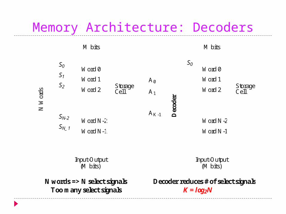
Memory Architecture: Decoders
Word 0
Word 1
Word 2
Word N-1
Word N-2
Input-Output
S0
S1
S2
SN-2
SN_1
(M bits)
StorageCell
M bitsN
Wor
ds
Word 0
Word 1
Word 2
Word N-1
Word N-2
Input-Output(M bits)
StorageCell
M bits
Dec
oder
A0
A1
AK-1
S0
N words => N select signalsToo many select signals
Decoder reduces # of select signalsK = log2N

Array-Structured memory Architecture
Input-Output(M bits)
Row
Dec
oder
AK
AK+1
AL-1
2L-K
Column Decoder
Bit Line
Word Line
A0
AK-1
Storage Cell
Sense Amplifiers / Drivers
M.2K
Problem: ASPECT RATIO or HEIGHT >> WIDTH
Amplify swing torail-to-rail amplitude
Selects appropriateword

Hierarchical memory Architecture
Global Data Bus
RowAddress
ColumnAddress
BlockAddress
Block Selector GlobalAmplifier/Driver
I/O
Control
Circuitry
Advantages:1. Shorter wires within blocks2. Block address activates only 1 block => power savings

Memory Timing Definitions
READ
WRITE
DATA
Read Access Read Access
Read Cycle
Data Valid
Data Written
Write Access
Write Cycle
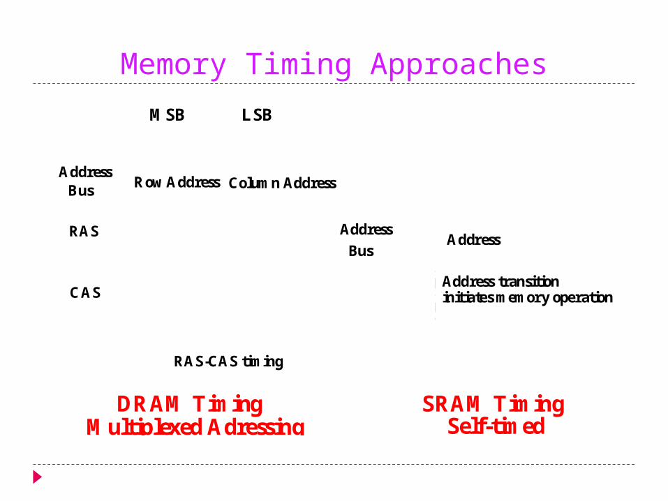
Memory Timing Approaches
AddressBus
RAS
CAS
RAS-CAS timing
Address
BusAddress
Address transitioninitiates memory operation
DRAM Timing SRAM Timing
Row Address Column Address
MSB LSB
Multiplexed Adressing Self-timed
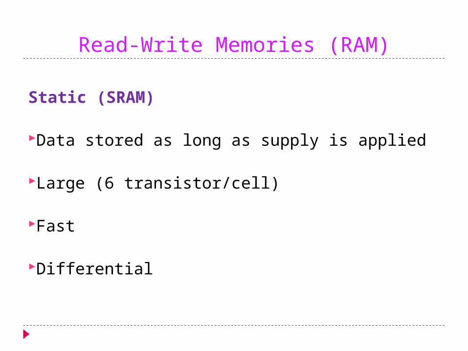
Read-Write Memories (RAM)
Static (SRAM)
Data stored as long as supply is applied
Large (6 transistor/cell)
Fast
Differential
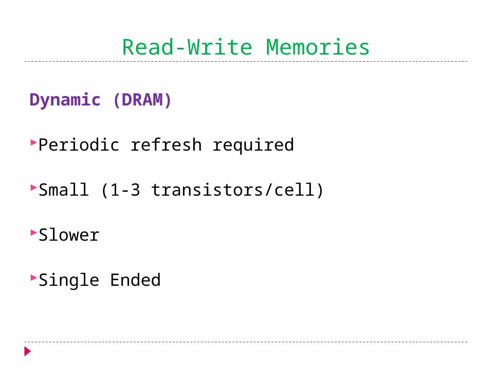
Read-Write Memories
Dynamic (DRAM)
Periodic refresh required
Small (1-3 transistors/cell)
Slower
Single Ended
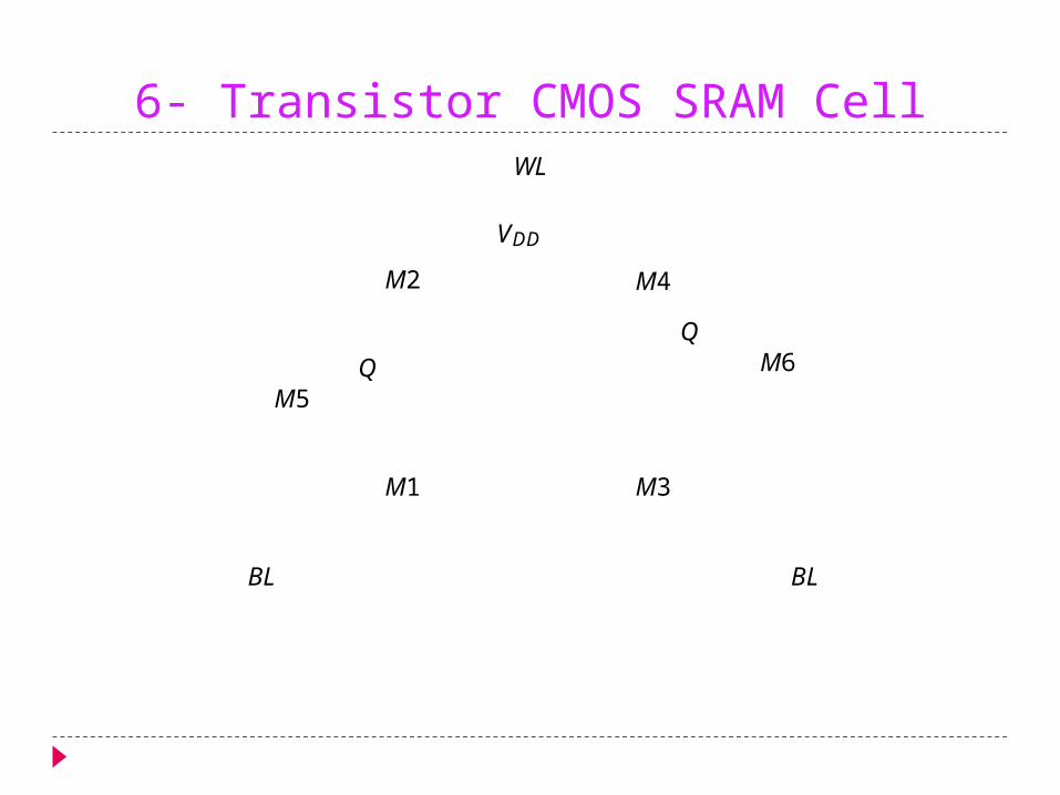
6- Transistor CMOS SRAM Cell
VDD
Q
Q
M1 M3
M4M2
M5
BL
WL
BL
M6

CMOS SRAM Analysis (Write)
VDD
Q = 1Q = 0
M1
M4
M5
BL = 1
WL
BL = 0
M6
VDD
kn M6 VDD VTn– VDD
2----------- VDD
2
8-----------–
kp M4 VDD VTp– VDD
2----------- VDD
2
8-----------–
=
kn M5
2--------------
VDD
2----------- VTn
VDD
2-----------
–
2
kn M1 VDD VTn– V DD
2-----------
VDD2
8-----------–
= (W/L)n,M510 (W/L)n,M1
(W/L)n,M60.33 (W/L)p,M4

CMOS SRAM Analysis (Read)
VDD
Q = 1Q = 0
M1
M4
M5
BL
WL
BL
M6
VDDVDD
VDD
CbitCbit
kn M5
2---------------
VDD
2------------ VTn
VDD
2------------
–
2kn M1 VDD VTn–
VDD
2------------
VDD2
8------------–
=
(W/L)n,M510 (W/L)n,M1 (supercedes read constraint)

6T- SRAM - Layout
VDD
GND
WL
BLBL
M1 M3
M4M2
M5 M6

3- Transistor DRAM Cell
M2M1
BL1
WWL
BL2
M3
RWL
CS
X
WWL
RWL
X
BL1
BL2
VDD-VT
V
VDD
VDD-VT
No constraints on device ratiosReads are non-destructiveValue stored at node X when writing a “1” = VWWL-VTn

3-T DRAM Layout
BL2 BL1 GND
RWL
WWL
M3
M2
M1

DRAM Cell
1T DRAM requires a sense amplifier for each
bit line, due to charge redistribution read-out.
DRAM Memory cells are single ended in
contrast to SRAM cells.

1-T DRAM cell
(a) Cross-section
(b) Layout
Diffusedbit line
Polysiliconplate
M1 wordline
Capacitor
Polysilicongate
Metal word line
SiO2
n+ Field Oxide
Inversion layerinduced by plate bias
n+
poly
poly
Used Polysilicon-Diffusion Capacitance
Expensive in Area
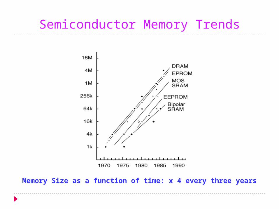
Semiconductor Memory Trends
Memory Size as a function of time: x 4 every three years

Semiconductor Memory Trends
Increasing die size factor 1.5 per generationCombined with reducing cell size factor 2.6 per generation

Semiconductor Memory Trends
Technology feature size for different SRAM generations

The End
……. Thank You …….
Recommended