Embed Size (px)
Citation preview
Semiconductor Memories:Semiconductor Memories:I t d tiI t d tiaan Introductionn Introduction

Talk OverviewTalk OverviewTalk OverviewTalk Overview
M T dMemory TrendMemory ClassificationMemory ClassificationMemory ArchitecturesThe Memory CoreP i hPeripheryReliabilityReliability
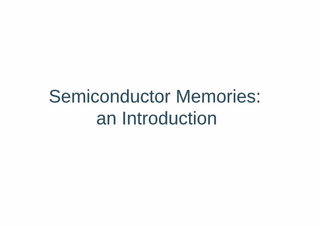
Semiconductor Memory TrendsSemiconductor Memory Trends( t th 90’ )( t th 90’ )(up to the 90’s)(up to the 90’s)
Memory Size as a function of time: x 4 every three years
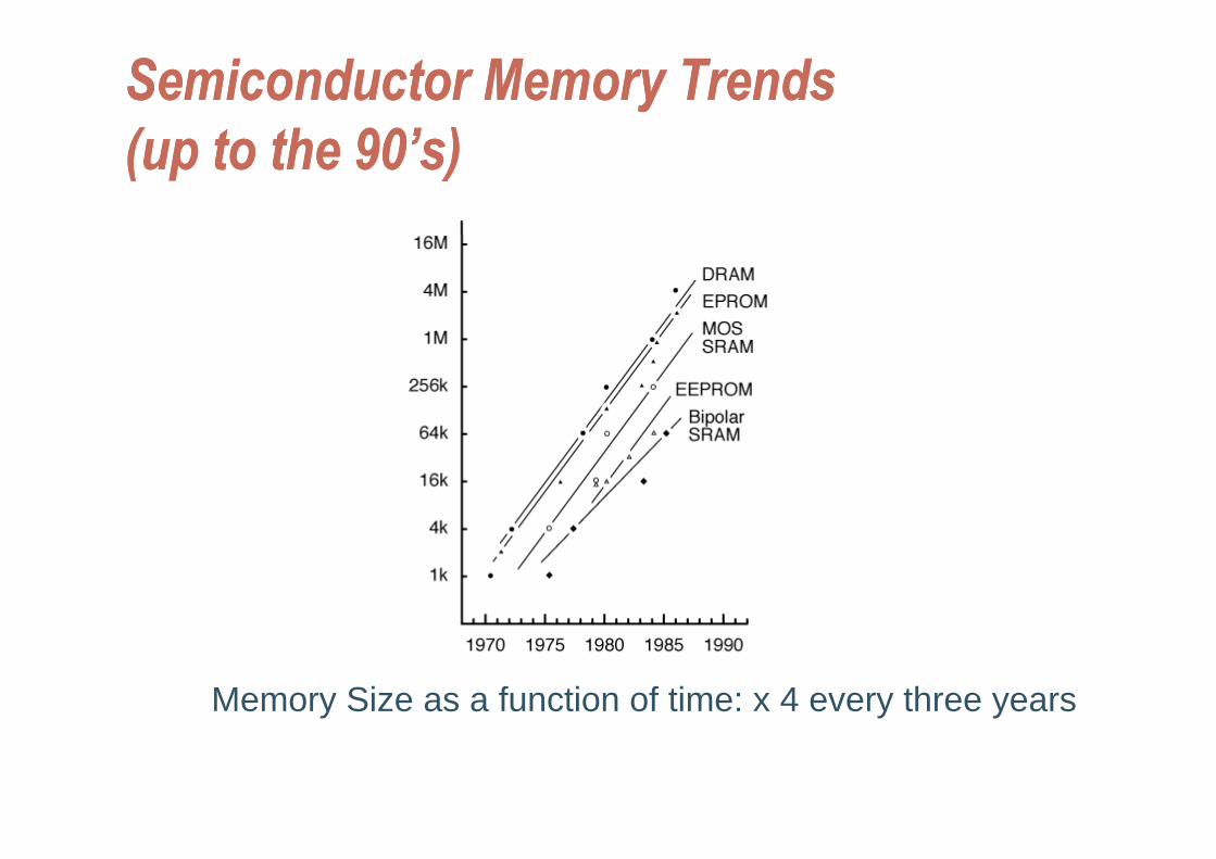
Semiconductor Memory TrendsSemiconductor Memory Trends( d t d)( d t d)(updated)(updated)
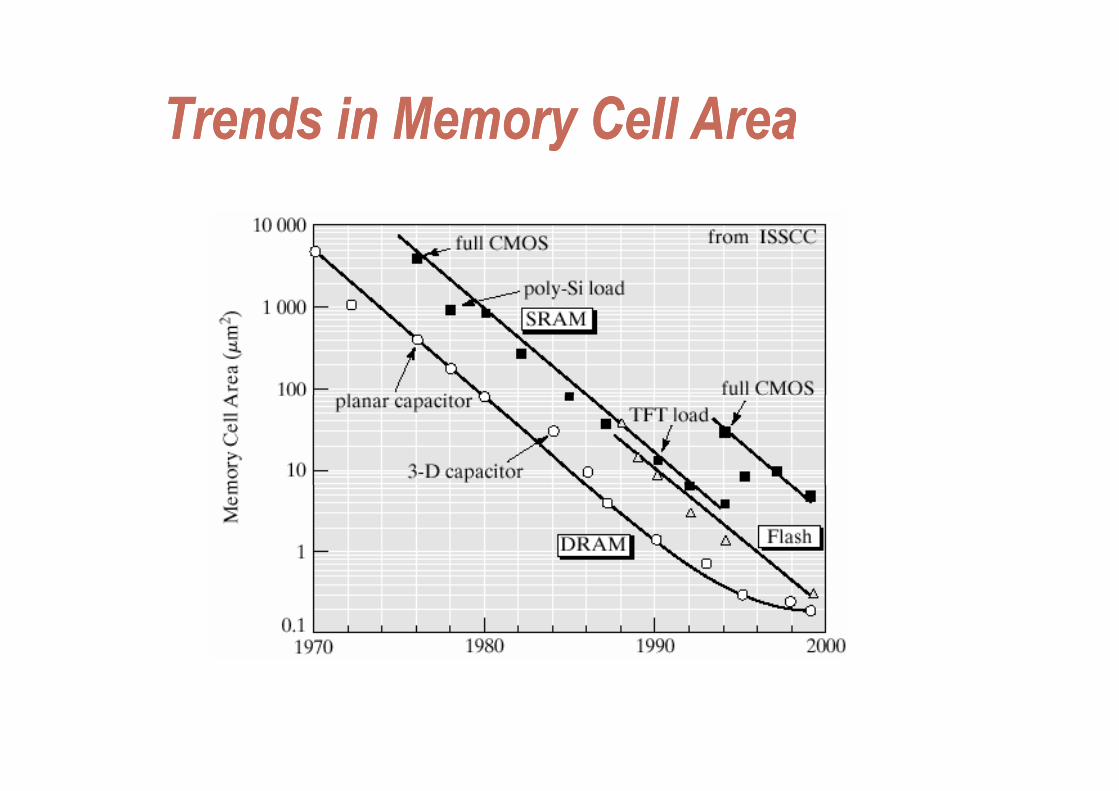
Trends in Memory Cell AreaTrends in Memory Cell AreaTrends in Memory Cell AreaTrends in Memory Cell Area
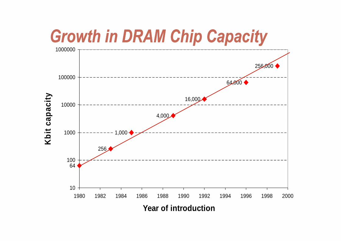
Growth in DRAM Chip CapacityGrowth in DRAM Chip CapacityGrowth in DRAM Chip CapacityGrowth in DRAM Chip Capacity256 000
1000000
64,000
256,000
100000
y
4,000
16,00010000
apac
ity
256
1,0001000
Kbi
t ca
64
256
100
101980 1982 1984 1986 1988 1990 1992 1994 1996 1998 2000
Year of introduction
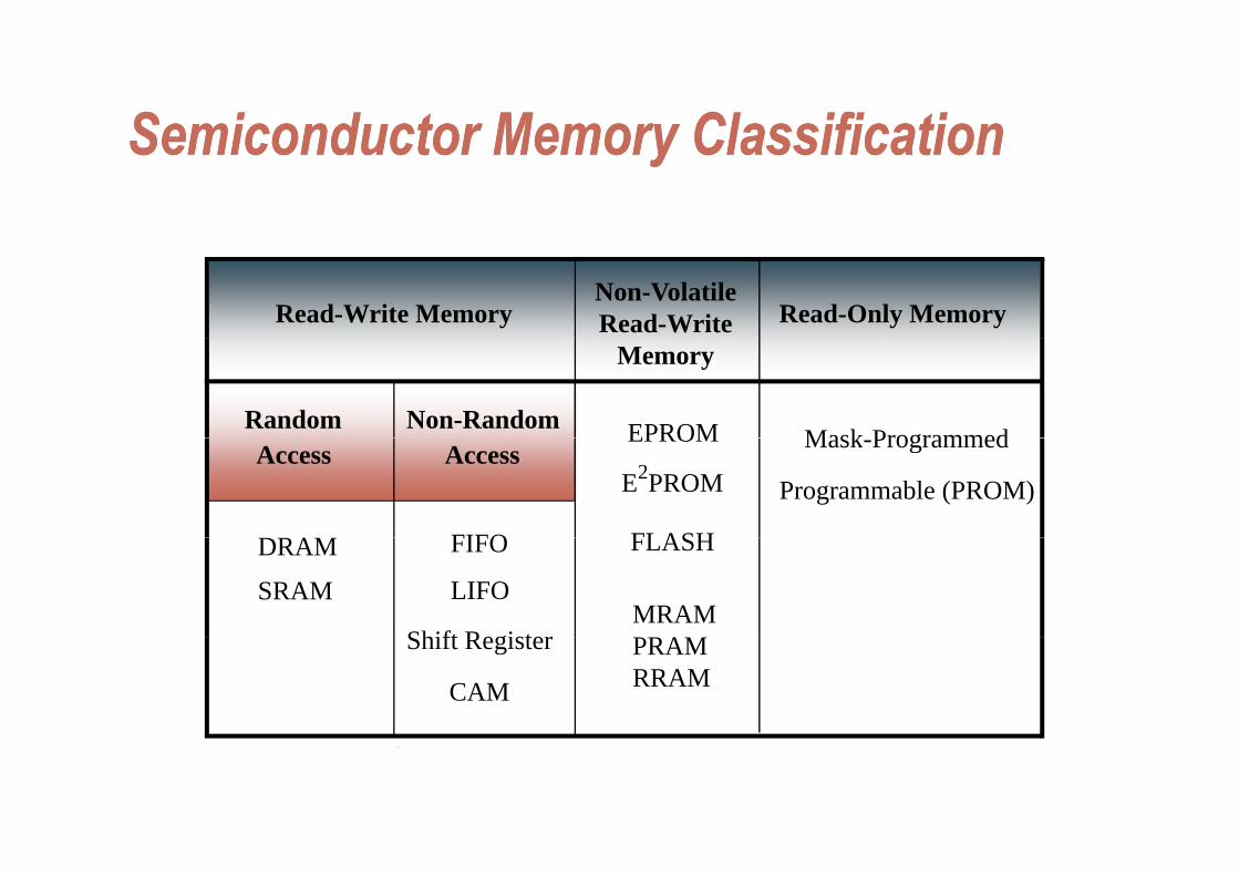
Semiconductor Memory ClassificationSemiconductor Memory ClassificationSemiconductor Memory ClassificationSemiconductor Memory Classification
Read-Write MemoryNon-VolatileRead-Write Read-Only Memory
Memory
EPROMRandom Non-RandomMask ProgrammedEPROM
E2PROM
FLASH
Access Access
A
Mask-Programmed
Programmable (PROM)
FIFO FLASH
SRAM
DRAM FIFO
Shift Register
LIFOMRAM
AShift Register
CAM
PRAMRRAM
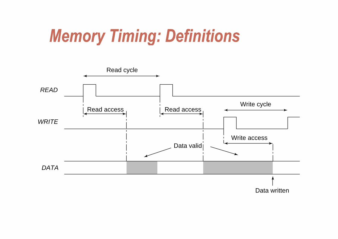
Memory Timing: DefinitionsMemory Timing: DefinitionsMemory Timing: DefinitionsMemory Timing: DefinitionsRead cycle
READ
Write cycleRead access Read access
WRITE
Write accessData valid
WRITE
Data valid
DATA
Data written
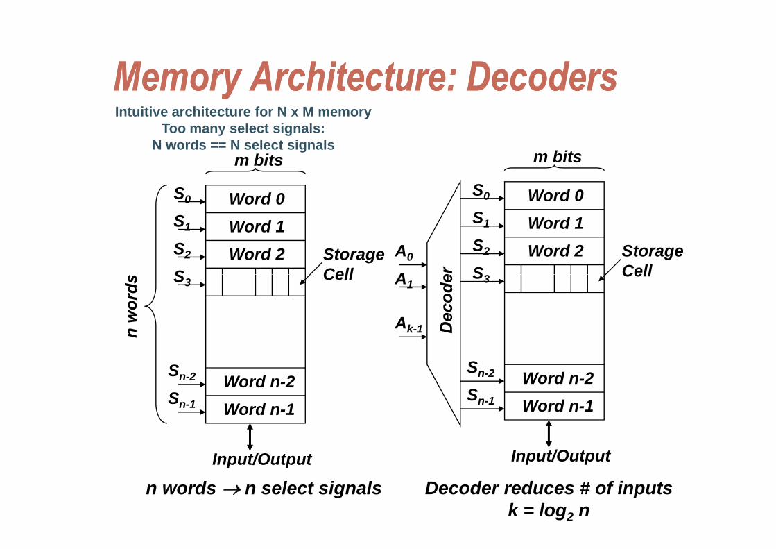
Memory Architecture: DecodersMemory Architecture: DecodersMemory Architecture: DecodersMemory Architecture: DecodersIntuitive architecture for N x M memory
Too many select signals:N words == N select signalsg
Word 0
m bits
S0 Word 0
m bits
S0
SWord 1Word 2 Storage
Cell
S1
S2
S
Word 1Word 2 Storage
Cell
S1
S2
SA0
ACellS3CellS3A1
Ak-1
Word n-2Sn-2
SWord n-2Sn-2
Sn 1Word n-1Sn-1
Input/Output
Word n-1Sn-1
Input/OutputInput/Output
n words → n select signals
put/Output
Decoder reduces # of inputsk = log2 n
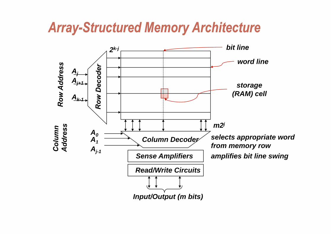
ArrayArray--Structured Memory ArchitectureStructured Memory Architecturebit line
word line2k-j
word line
storage
AjAj+1
(RAM) cellAk-1
A0A1 Column Decoder
m2j
selects appropriate word fAj-1
Sense Amplifiers
Read/Write Circuits
amplifies bit line swingfrom memory row
Read/Write Circuits
Input/Output (m bits)Input/Output (m bits)
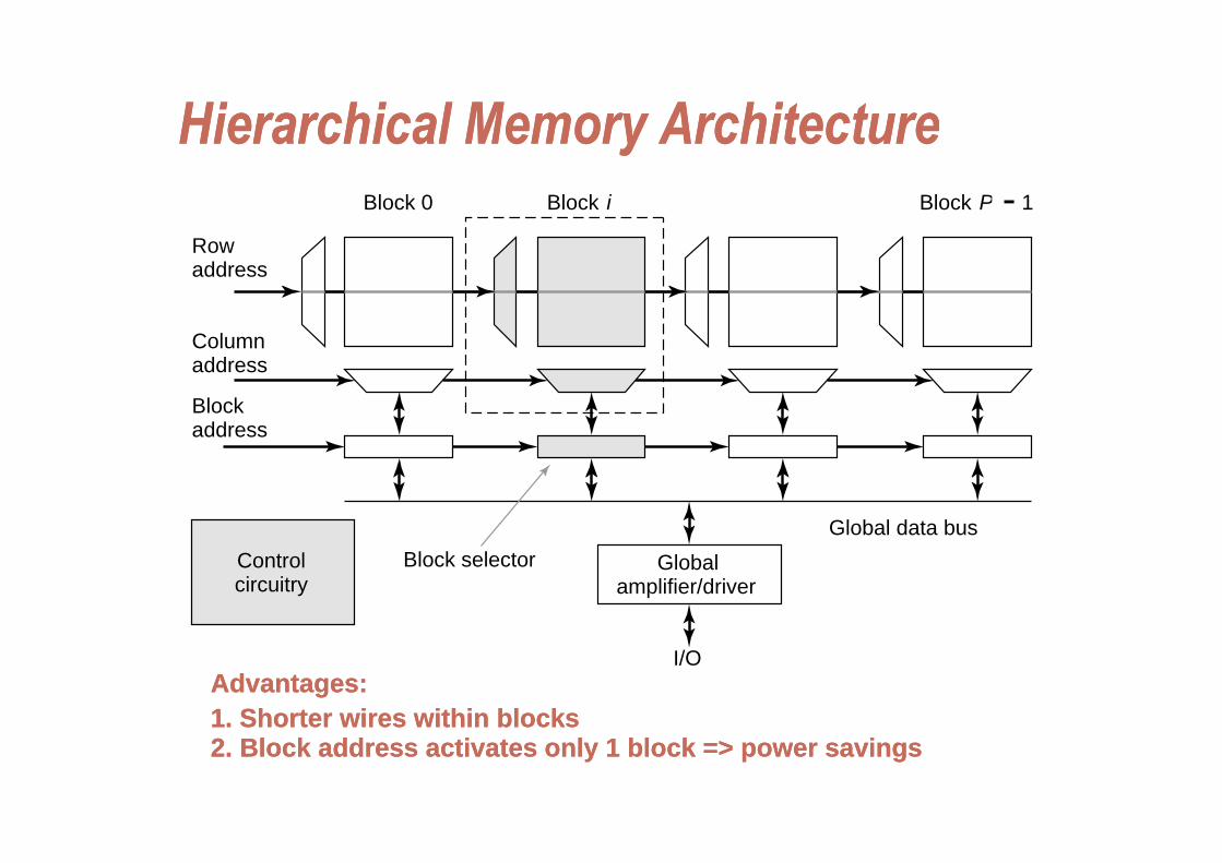
Hierarchical Memory ArchitectureHierarchical Memory ArchitectureHierarchical Memory ArchitectureHierarchical Memory ArchitectureBlock 0 Block i Block P 2 1-
Rowaddress
C lColumnaddress
Blockaddress
Global data bus
address
Globalamplifier/driver
Controlcircuitry
Global data busBlock selector
Advantages:Advantages:1. Shorter wires within blocks1. Shorter wires within blocks
I/O
1. Shorter wires within blocks1. Shorter wires within blocks2. Block address activates only 1 block => power savings2. Block address activates only 1 block => power savings
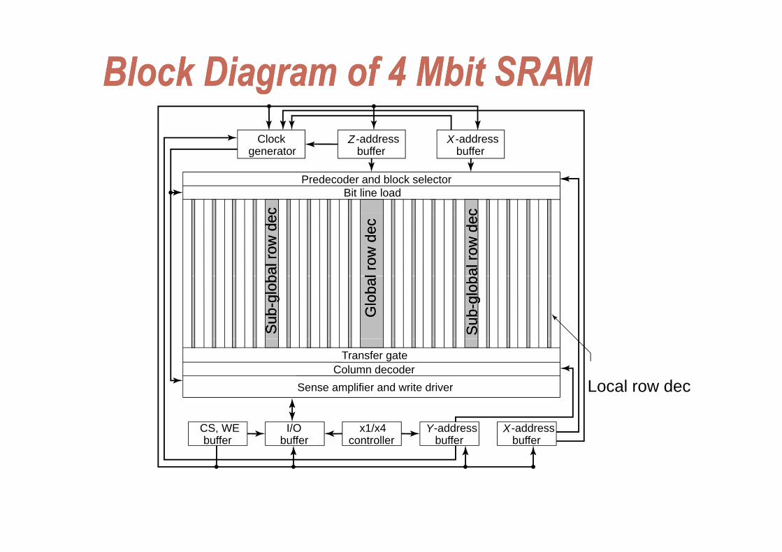
Block Diagram of 4 Mbit SRAMBlock Diagram of 4 Mbit SRAMggClock
generatorZ-address
bufferX-address
buffergenerator buffer buffer
Predecoder and block selectorBit line load
cccc
l row
l r
ow d
ecdec
al ro
w
al ro
w d
e cdec
bal r
ow
bal r
ow d
ecdec
Glo
bal
Glo
bal
Sub
Sub
--glo
bgl
ob
Sub
Sub
--glo
bgl
ob
Transfer gateColumn decoder
Sense amplifier and write driver Local row dec
CS, WEbuffer
I/Obuffer
Y-addressbuffer
X-addressbuffer
x1/x4controller
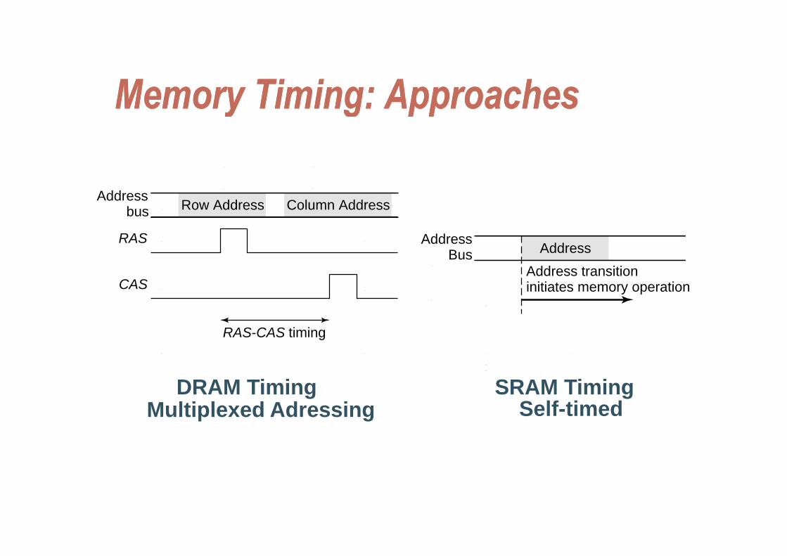
Memory Timing: ApproachesMemory Timing: ApproachesMemory Timing: ApproachesMemory Timing: Approaches
Addressbus Row Address Column Addressbus
RAS AddressBus
Address transitionAddress
RAS-CAS timing
initiates memory operationCAS
DRAM TimingM lti l d Ad i
SRAM TimingS lf ti dMultiplexed Adressing Self-timed
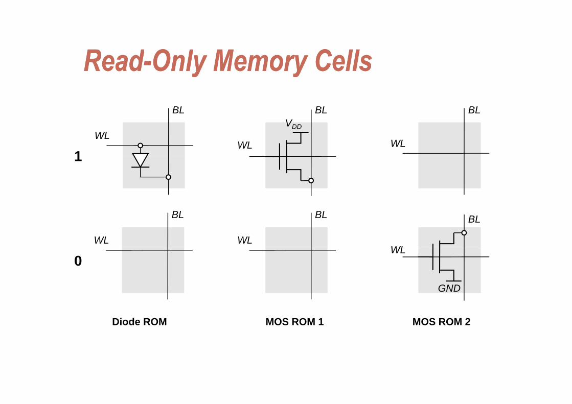
ReadRead--Only Memory CellsOnly Memory CellsReadRead--Only Memory CellsOnly Memory CellsBL BLBL
WL
BL
WL
BL
1WL
BLVDD
1
WL
BL
WL
BL
WL
BL
0WL
GND
Diode ROM MOS ROM 1 MOS ROM 2
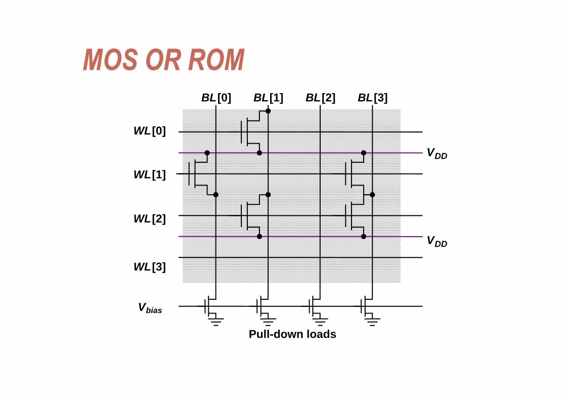
MOS OR ROMMOS OR ROMMOS OR ROMMOS OR ROMBL[0] BL[1] BL[2] BL[3]
WL[0]
VDDVDD
WL[1]
WL[2]
VDD
WL[3]
DD
Vbias
Pull-down loadsPull down loads
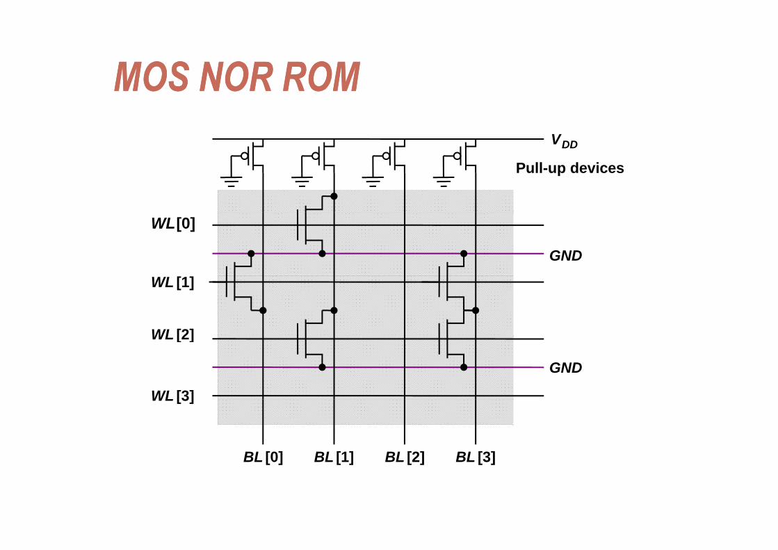
MOS NOR ROMMOS NOR ROMMOS NOR ROMMOS NOR ROMVDD
Pull-up devices
WL[0]
GND
WL [1]
WL [2]WL [2]
WL [3]
GND
BL [0]
WL [3]
BL [1] BL [2] BL [3][ ] [ ] [ ] [ ]
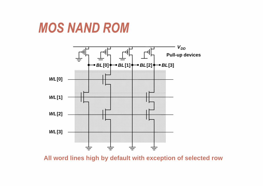
MOS NAND ROMMOS NAND ROMMOS NAND ROMMOS NAND ROMVDD
Pull-up devices
BL[3]BL[2]BL[1]BL [0]
WL [0]
WL [1]
WL [2]WL [2]
WL [3]
All d li hi h b d f lt ith ti f l t dAll word lines high by default with exception of selected row
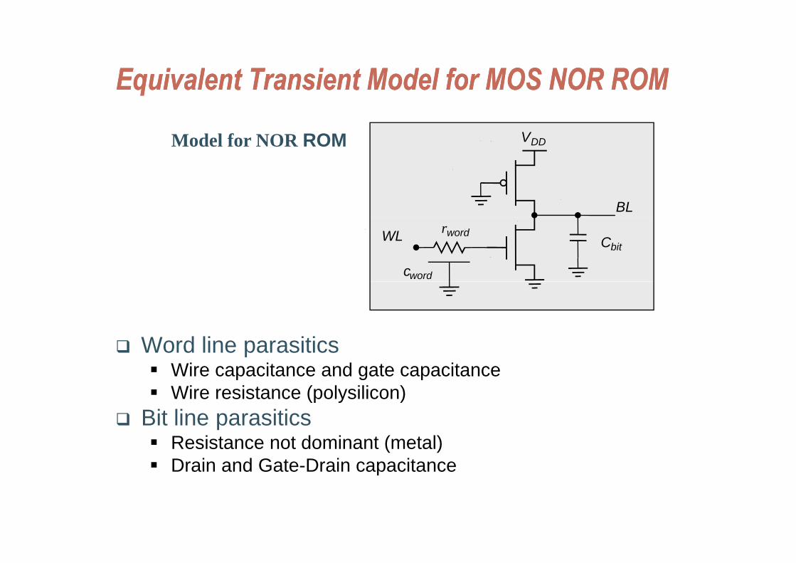
Equivalent Transient Model for MOS NOR ROMEquivalent Transient Model for MOS NOR ROMqu a e t a s e t ode o OS O Oqu a e t a s e t ode o OS O O
Model for NOR ROM VDD
BL
Cbit
rword
cword
WL
Word line parasiticsWord line parasiticsWire capacitance and gate capacitanceWire resistance (polysilicon)
Bi li i iBit line parasiticsResistance not dominant (metal)Drain and Gate-Drain capacitancep
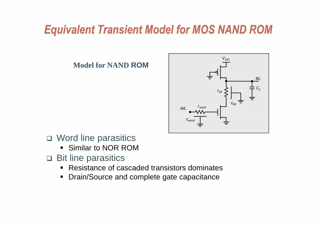
Equivalent Transient Model for MOS NAND ROMEquivalent Transient Model for MOS NAND ROMqq
VDD
Model for NAND ROM
C
BL
CL
rwordcbit
rbit
WL
Word line parasitics
cword
Word line parasiticsSimilar to NOR ROM
Bit line parasiticsResistance of cascaded transistors dominatesDrain/Source and complete gate capacitance
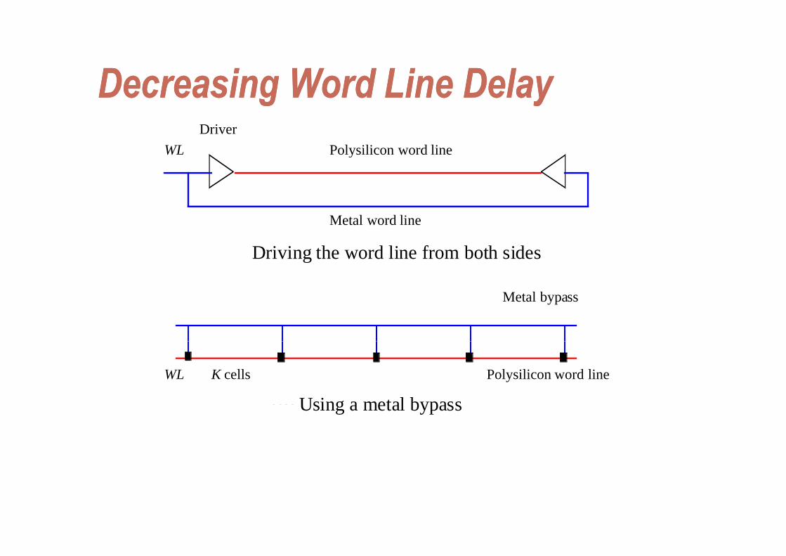
Decreasing Word Line DelayDecreasing Word Line DelayDecreasing Word Line DelayDecreasing Word Line DelayPolysilicon word lineWL
DriverPolysilicon word lineWL
l d li
(a) Driving the word line from both sides
Metal word line
Metal bypass
Polysilicon word lineK cells
(b) Using a metal bypass
WL
(b) Using a metal bypass
(c) Use silicides
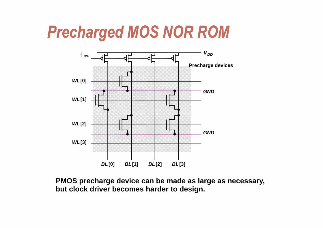
Precharged MOS NOR ROMPrecharged MOS NOR ROMPrecharged MOS NOR ROMPrecharged MOS NOR ROMVDDpref
WL [0]
Precharge devices
GNDWL [1]
WL [2]
GND
BL [0]
WL [3]
BL [1] BL [2] BL [3]
PMOS precharge device can be made as large as necessary,but clock driver becomes harder to design.
[0] [ ] [ ] [3]
g
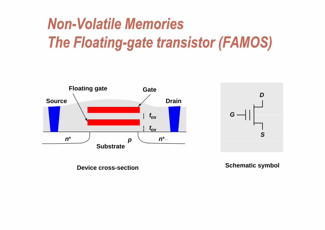
NonNon--Volatile MemoriesVolatile MemoriesTh Fl iTh Fl i i (FAMOS) i (FAMOS)The FloatingThe Floating--gate transistor (FAMOS)gate transistor (FAMOS)
Floating gate GateFloating gate
Source
Gate
Drain
t G
D
n+ n+_p
tox
tox
G
S
Substratep
Device cross section Schematic symbolDevice cross-section Schematic symbol
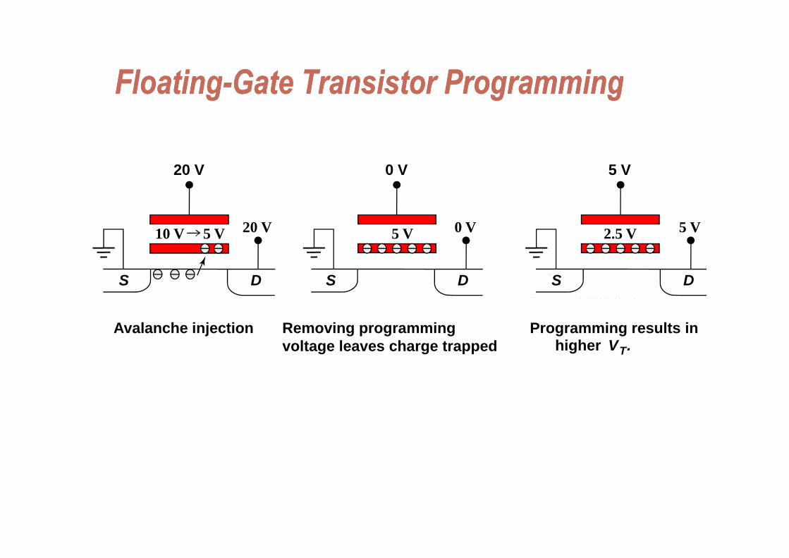
FloatingFloating--Gate Transistor ProgrammingGate Transistor ProgrammingFloatingFloating Gate Transistor ProgrammingGate Transistor Programming
0 V 5 V20 V
5 V 0 V
DS
2.5 V 5 V
DS
10 V 5 V 20 V
DS DS
Removing programming lt l h t d
DS
Programming results inhi h V
DS
Avalanche injectionvoltage leaves charge trapped higher VT.
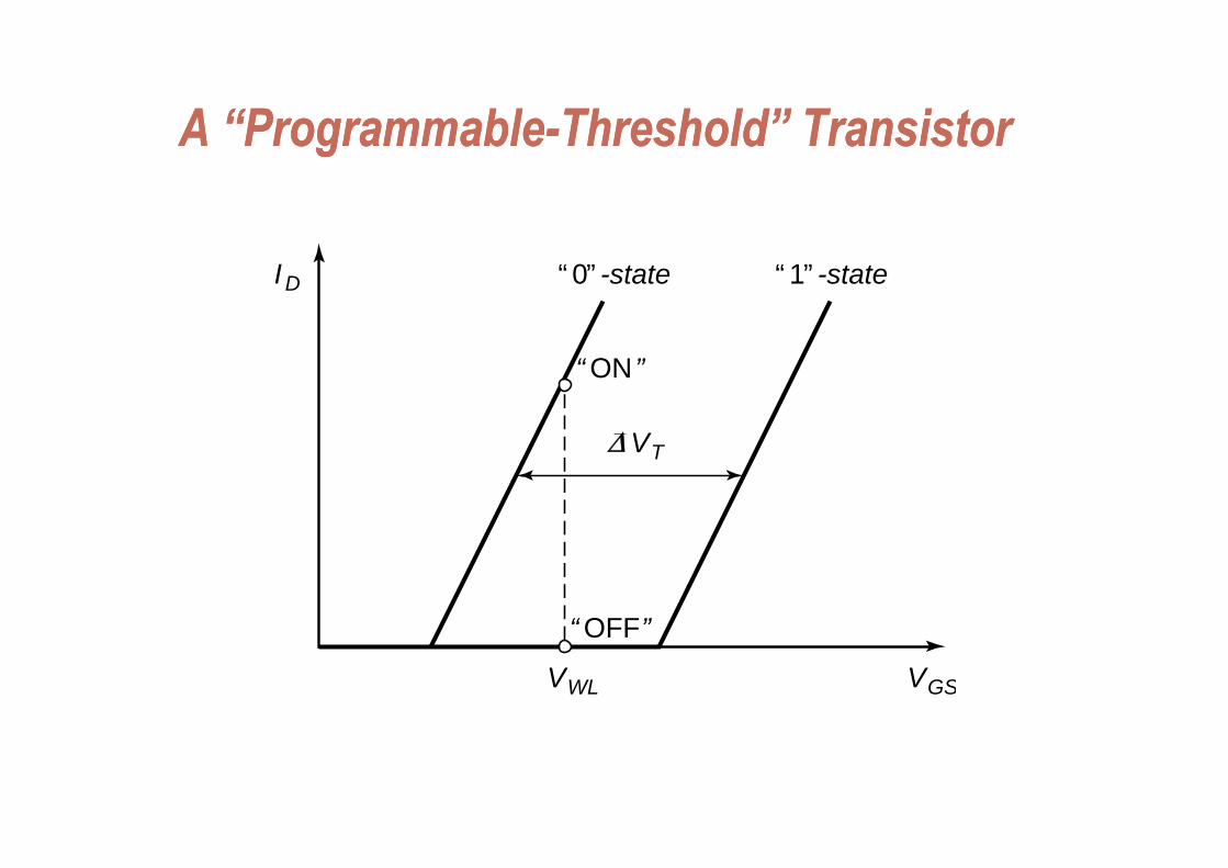
A “ProgrammableA “Programmable--Threshold” TransistorThreshold” TransistorA ProgrammableA Programmable Threshold TransistorThreshold Transistor
“ 0” -state “ 1” -stateID
DV
“ ON ”
ΔDVTΔ
“ OFF”
VWL VGS
OFF
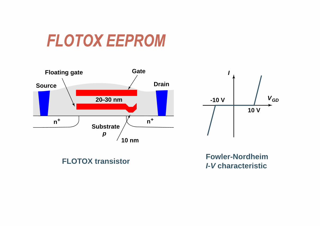
FLOTOX EEPROMFLOTOX EEPROMFLOTOX EEPROMFLOTOX EEPROMFloating gate
Source
Gate
Drain
I
Source
20–30 nm -10 V10 V
VGD
Substratep
n1 n1
10
n+ n+
FLOTOX transistor Fowler-Nordheim I V characteristic
10 nm
I-V characteristic
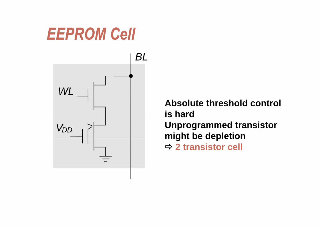
EEPROM CellEEPROM CellEEPROM CellEEPROM CellBL
WLWLAbsolute threshold controlis hard
VDD
is hardUnprogrammed transistor might be depletionmight be depletion
2 transistor cell
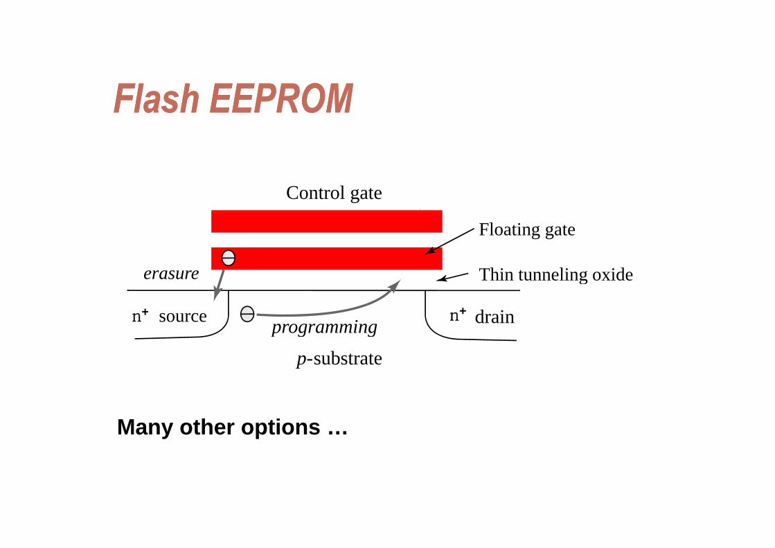
Fl h EEPROMFl h EEPROMFlash EEPROMFlash EEPROM
Control gate
erasure
Floating gate
Thin tunneling oxideerasure Thin tunneling oxide
n 1 source n1 drainprogrammingn+ n+
p-substratep g g
Many other options …
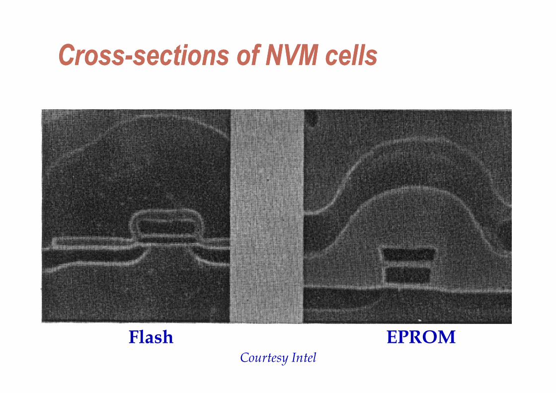
CrossCross--sections of NVM cellssections of NVM cellsCrossCross sections of NVM cellssections of NVM cells
Ol h EPROMFlashCourtesy Intel
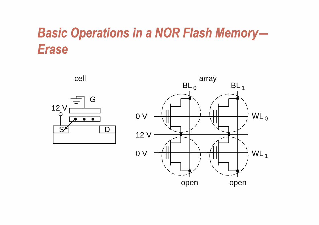
Basic Operations in a NOR Flash Memory―Basic Operations in a NOR Flash Memory―Basic Operations in a NOR Flash MemoryBasic Operations in a NOR Flash MemoryEraseErase
cell arrayBL 0 BL 1
12 VG
BL 0 BL 1
S D
WL 00 V
12 V
WL 10 V
open open
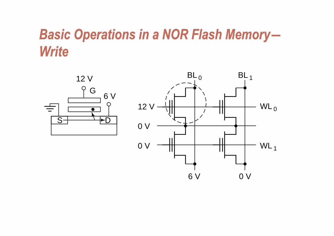
Basic Operations in a NOR Flash Memory―Basic Operations in a NOR Flash Memory―Basic Operations in a NOR Flash MemoryBasic Operations in a NOR Flash MemoryWriteWrite
12 VG
BL 0 BL 1
S D
6 VG
WL 012 V
S D
WL0 V
0 V
WL 10 V
6 V 0 V
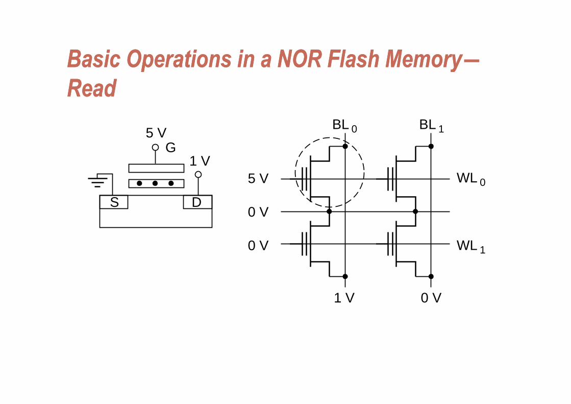
Basic Operations in a NOR Flash Memory―Basic Operations in a NOR Flash Memory―Basic Operations in a NOR Flash MemoryBasic Operations in a NOR Flash MemoryReadRead
5 V
1 VG
BL 0 BL 1
1 V
S D
WL 05 V
S D
WL 10 V
0 V
1 V 0 V
WL 10 V
1 V 0 V
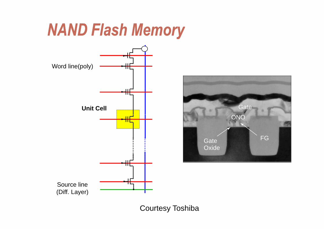
NAND Flash MemoryNAND Flash Memoryyy
Word line(poly)
Unit Cell GateONO
FGGateGateOxide
Source line(Diff Layer)(Diff. Layer)
Courtesy Toshiba
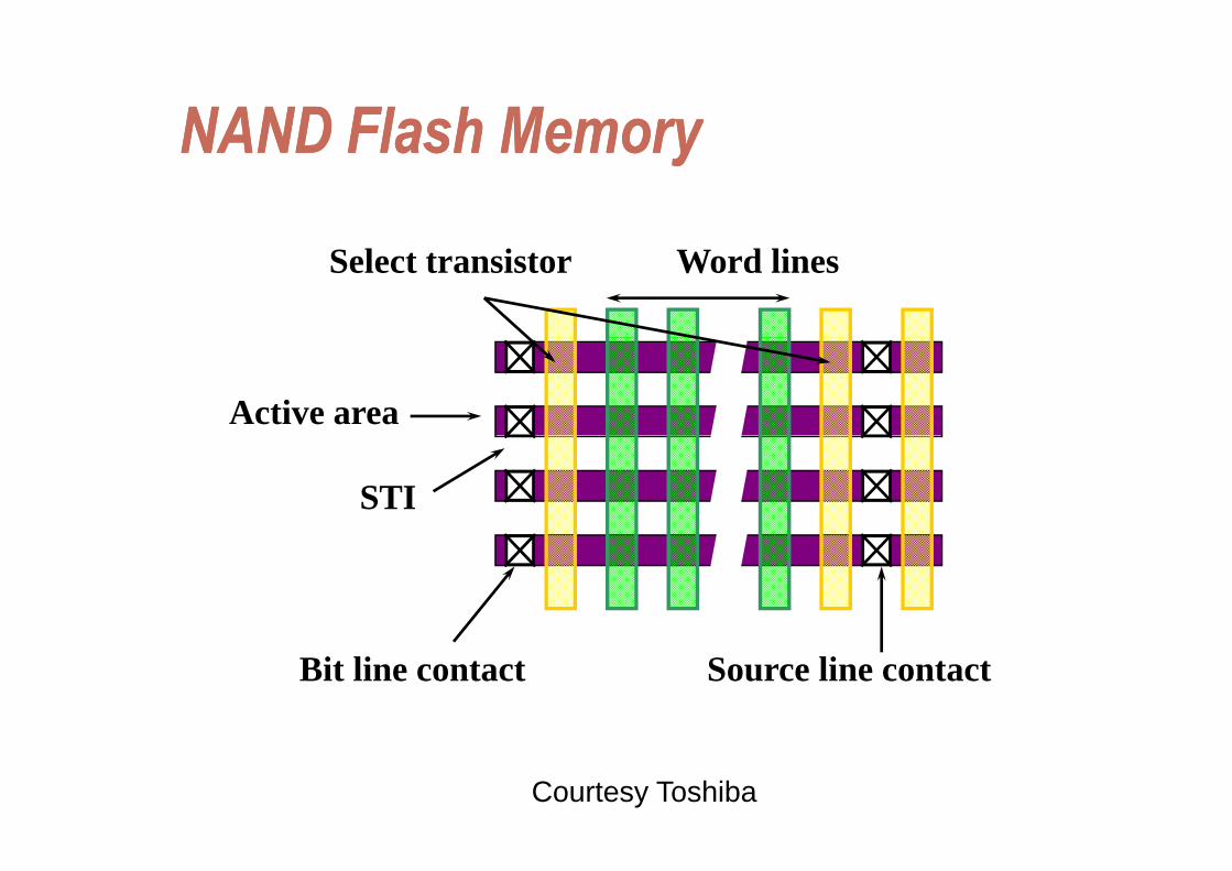
NAND Flash MemoryNAND Flash MemoryNAND Flash MemoryNAND Flash Memory
Word linesSelect transistor
Active area
STI
Bit line contact Source line contact
Courtesy Toshiba
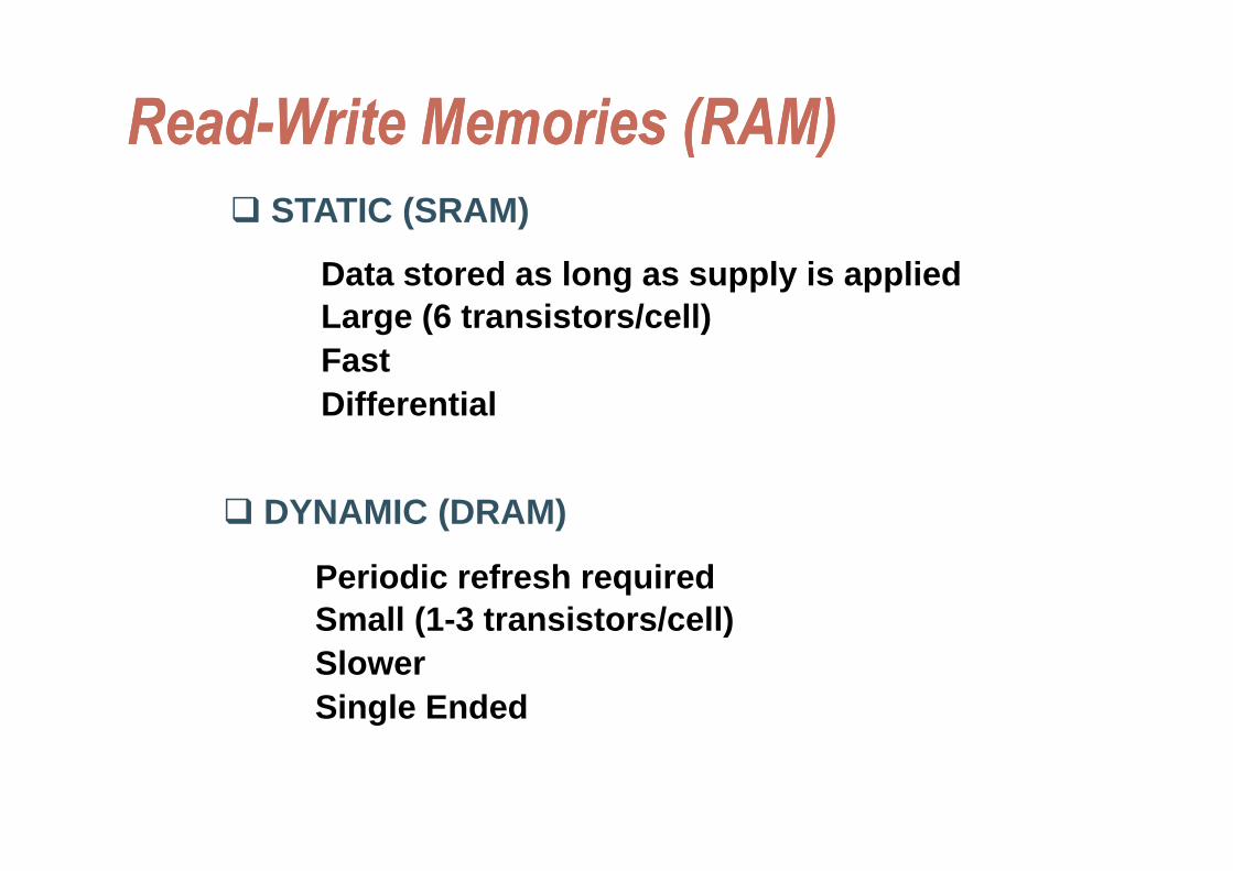
ReadRead--Write Memories (RAM)Write Memories (RAM)ReadRead Write Memories (RAM)Write Memories (RAM)STATIC (SRAM)
Data stored as long as supply is appliedLarge (6 transistors/cell)FastDifferential
DYNAMIC (DRAM)
Periodic refresh requiredSmall (1-3 transistors/cell)( )SlowerSingle Ended
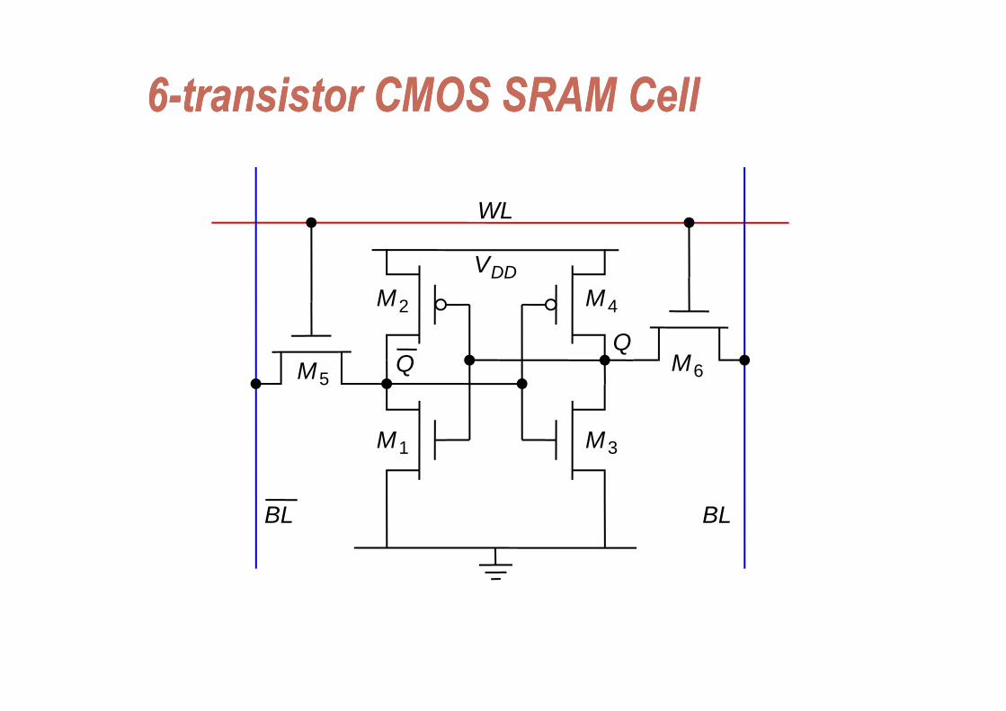
66--transistor CMOS SRAM Cell transistor CMOS SRAM Cell
WL
VDDDD
M
M4M2
QQM5
M6
M M
Q
BL
M1 M3
BL BLBL
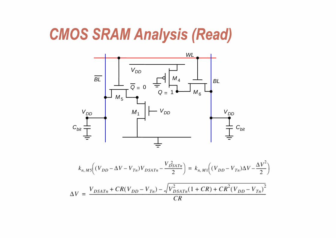
CMOS SRAM Analysis (Read)CMOS SRAM Analysis (Read)CMOS SRAM Analysis (Read)CMOS SRAM Analysis (Read)WL
BL
VDD
M
M 4BL
Q 1Q = 0
M 5M 6
M1 VDDVDD VDD
Q = 1
Cbit Cbit
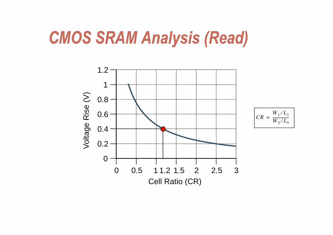
CMOS SRAM Analysis (Read)CMOS SRAM Analysis (Read)CMOS SRAM Analysis (Read)CMOS SRAM Analysis (Read)
1
1.2
0.6
0.8
Ris
e (V
)
0 2
0.4
Volta
ge R
00
0.2
0 5 1 1 2 1 5 2 2 5 3
V
0 0.5 1 1.2 1.5 2Cell Ratio (CR)
2.5 3
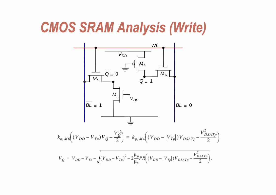
CMOS SRAM Analysis (Write) CMOS SRAM Analysis (Write) CMOS SRAM Analysis (Write) CMOS SRAM Analysis (Write) V
WL
Q = 0
M4
M6
VDD
Q 0Q = 1
M1
M56
VBL = 1 BL = 0
VDD
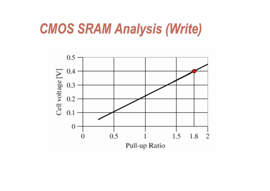
CMOS SRAM Analysis (Write)CMOS SRAM Analysis (Write)CMOS SRAM Analysis (Write)CMOS SRAM Analysis (Write)
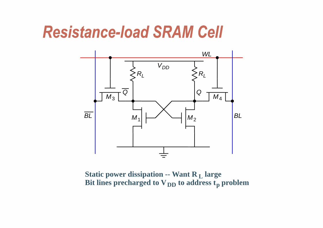
ResistanceResistance--load SRAM Cellload SRAM CellResistanceResistance load SRAM Cellload SRAM CellWL
RL RL
VDD
M3Q Q
M4
BL BLM1 M2BL BL
Static power dissipation -- Want R L largeBit lines precharged to VDD to address tp problem
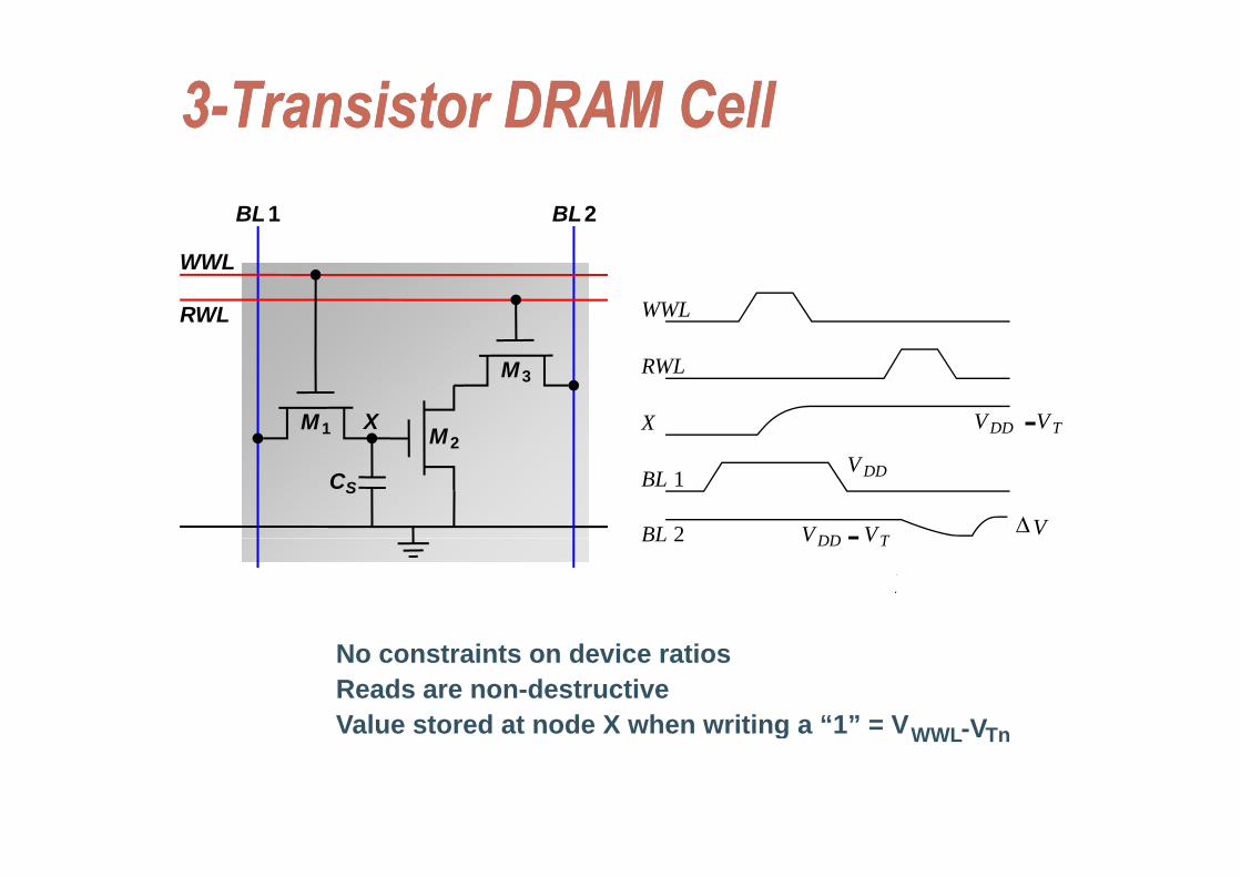
33--Transistor DRAM CellTransistor DRAM CellBL1 BL2
WWL
RWL WWL
M1 X
M3
M2VDD 2 VTX
RWL
-M2
CSV DD
D VV DD 2 VTBL 2
BL 1
- ΔV DD 2 VTBL 2 -
No constraints on device ratiosReads are non-destructiveValue stored at node X when writing a “1” = VWWL-VTng WWL Tn
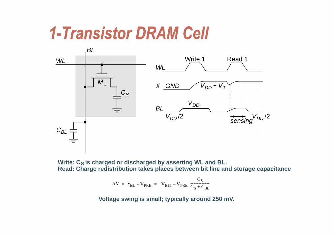
11--Transistor DRAM CellTransistor DRAM Cell11 Transistor DRAM CellTransistor DRAM CellWL
BLWrite 1 Read 1
M1
CVDD 2 VT
WL
X GND -CS
BLVDD
VDD /2 VDD /2
CBL
sensingVDD /2 VDD /2
Write: CS is charged or discharged by asserting WL and BL.Read: Charge redistribution takes places between bit line and storage capacitanceg p g p
Voltage swing is small; typically around 250 mV
ΔV BL VPRE– VBIT VPRE–CS
CS CBL+------------= =V
Voltage swing is small; typically around 250 mV.
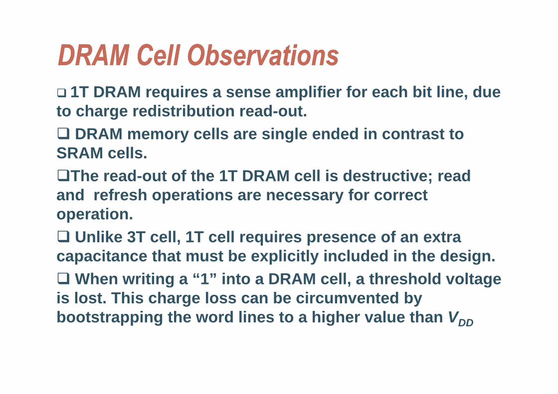
DRAM Cell ObservationsDRAM Cell ObservationsDRAM Cell ObservationsDRAM Cell Observations1T DRAM requires a sense amplifier for each bit line, due
t h di t ib ti d tto charge redistribution read-out.DRAM memory cells are single ended in contrast to
SRAM cellsSRAM cells.The read-out of the 1T DRAM cell is destructive; read
and refresh operations are necessary for correctand refresh operations are necessary for correct operation.
Unlike 3T cell, 1T cell requires presence of an extraUnlike 3T cell, 1T cell requires presence of an extra capacitance that must be explicitly included in the design.
When writing a “1” into a DRAM cell, a threshold voltage g , gis lost. This charge loss can be circumvented by bootstrapping the word lines to a higher value than VDD
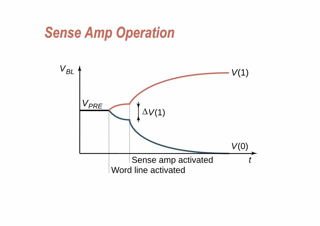
Sense Amp OperationSense Amp OperationSense Amp OperationSense Amp Operation
V(1)VBL
D V(1)VPRE
ΔD V(1)Δ
V(0)tSense amp activatedp
Word line activated
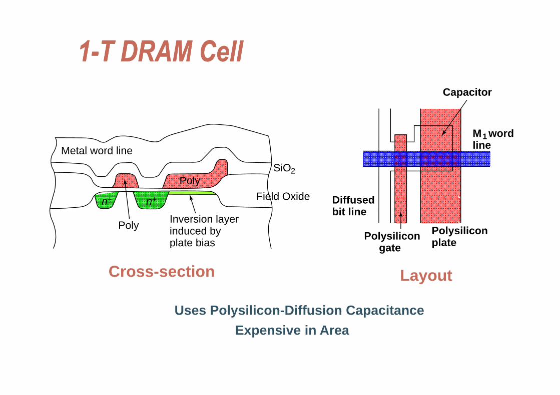
11--T DRAM CellT DRAM CellCapacitor
M1 wordlineMetal word line
Diff d
Metal word lineSiO2
Field Oxide+ +
Poly
Diffusedbit line
Polysilicon Polysiliconplate
Poly
Field Oxiden+ n+
Inversion layerinduced byplate bias gate plate
Cross-section Layout
plate bias
Uses Polysilicon-Diffusion CapacitanceExpensive in AreaExpensive in Area
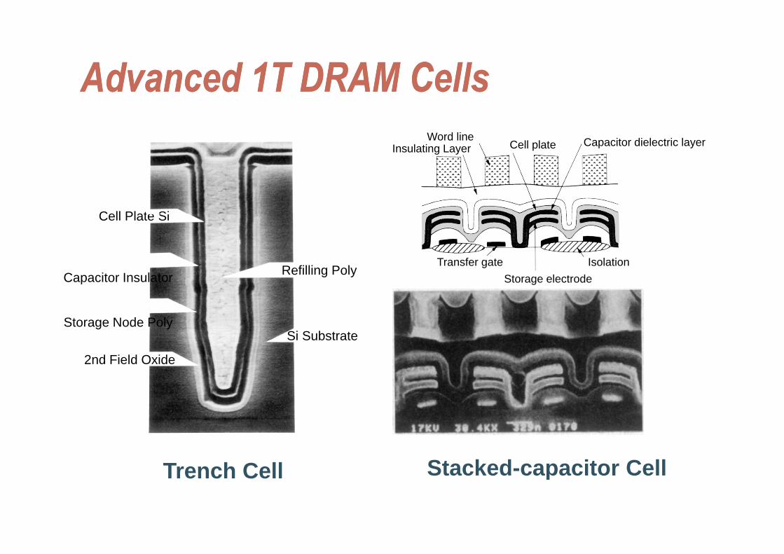
Advanced 1T DRAM CellsAdvanced 1T DRAM CellsAdvanced 1T DRAM CellsAdvanced 1T DRAM CellsCapacitor dielectric layerCell plate
Word lineInsulating Layer
Cell Plate Si
Insulating Layer
Cell Plate Si
Capacitor Insulator Refilling PolyIsolationTransfer gate
Storage electrodeCapacitor Insulator
Storage Node Poly
g y
Si Substrate
Storage electrode
2nd Field Oxide
Si Substrate
T h C ll Stacked capacitor CellTrench Cell Stacked-capacitor Cell
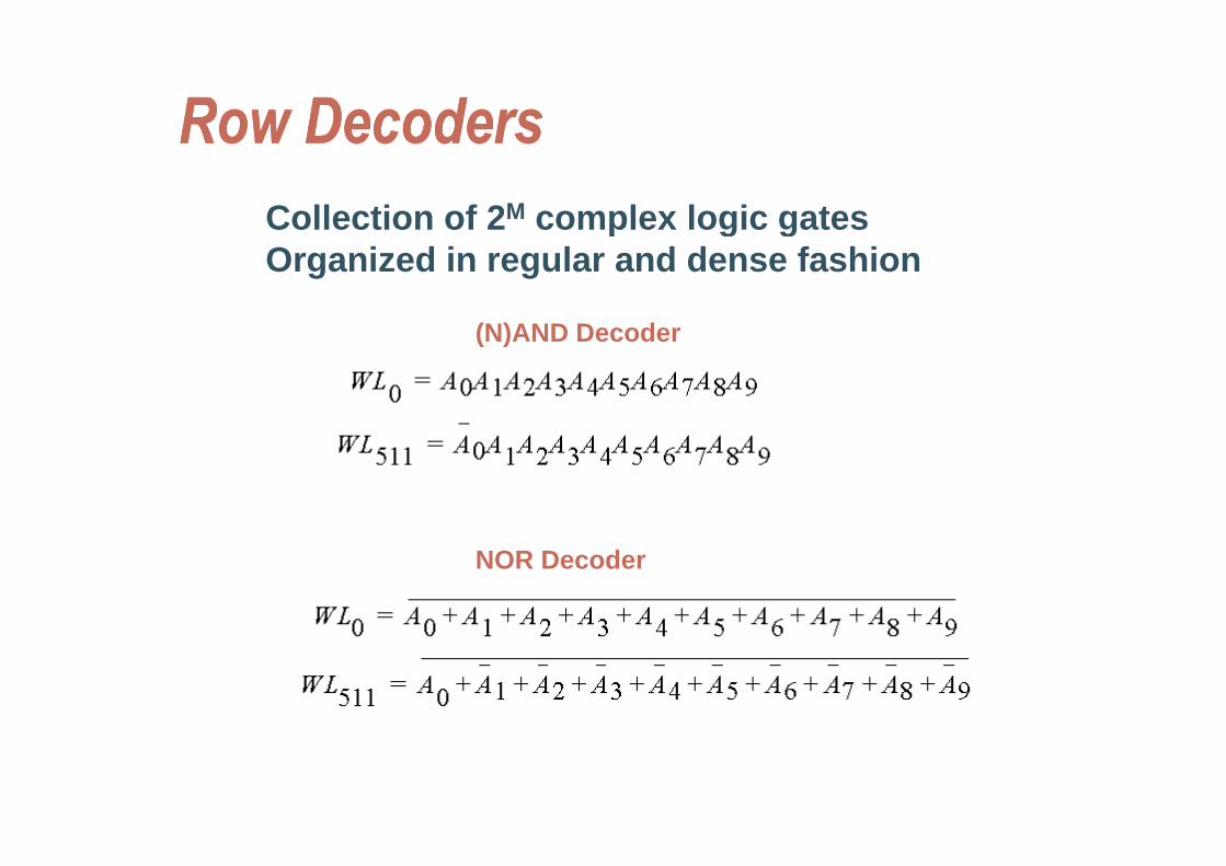
Row DecodersRow DecodersRow DecodersRow DecodersCollection of 2M complex logic gatesg gOrganized in regular and dense fashion
(N)AND Decoder(N)AND Decoder
NOR Decoder
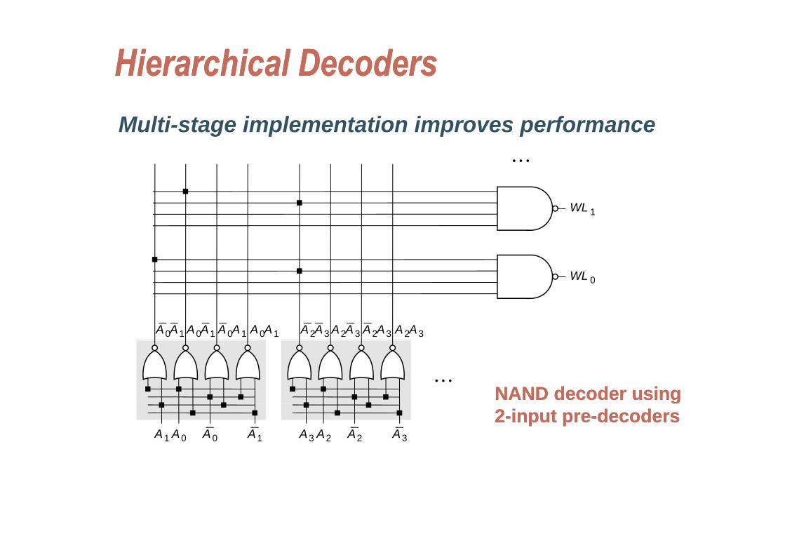
Hierarchical DecodersHierarchical DecodersMulti-stage implementation improves performance
• • •
WL 1
WL 0
1
A2A3
WL 0
A2A3A2A3A2A3A0A1A0A1A0A1A0A1
• • •
NAND decoder usingNAND decoder using
A2A2A3 A3A0A0A1 A1
gg22--input preinput pre--decodersdecoders
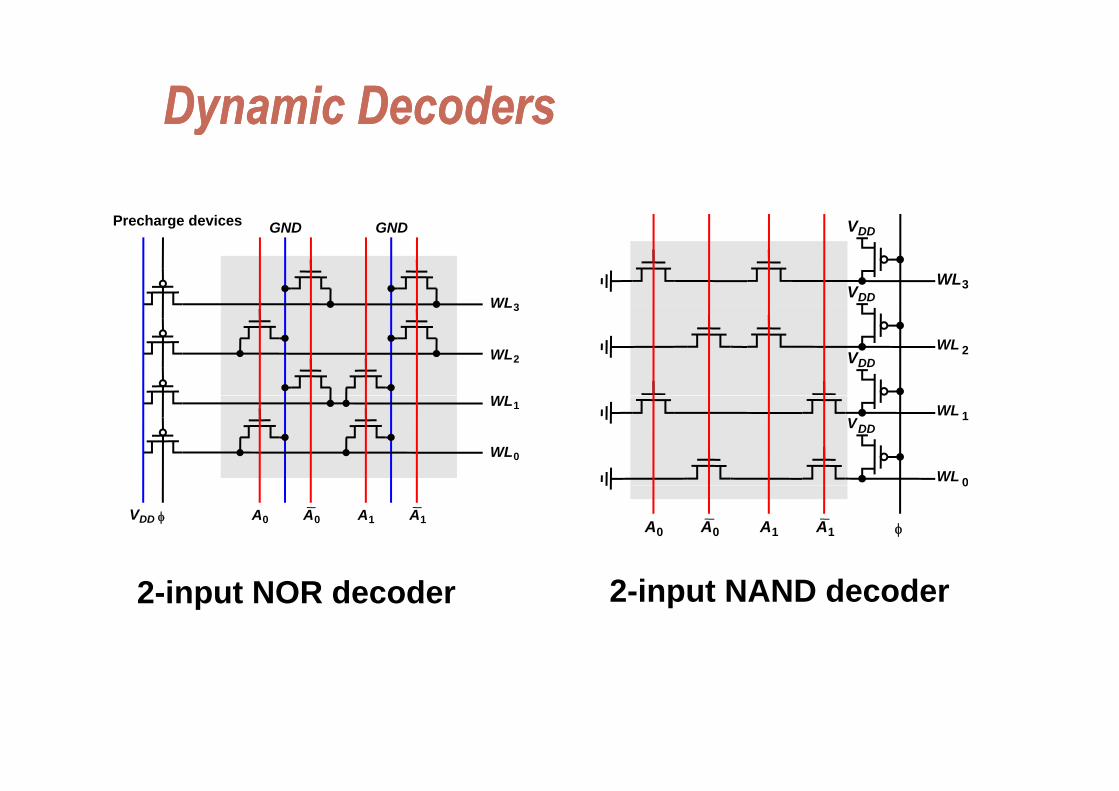
Dynamic DecodersDynamic Decodersyy
P h d iPrecharge devices GND
WL3
GND
WL3
VDD
VDDWL3
WL2
WL
WL 2VDD
WL1
WL0
WL 1
WL 0
VDD
VDD φ A0A0 A1A1φA0A0 A1A1
0
2-input NOR decoder 2-input NAND decoder
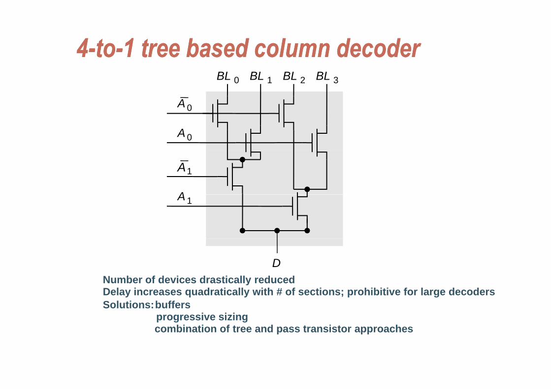
44--toto--1 tree based column decoder1 tree based column decoderBL 0 BL 1 BL 2 BL 3
A 0A 0
A 0
A1
AA 1
Number of devices drastically reducedD
Number of devices drastically reducedDelay increases quadratically with # of sections; prohibitive for large decoders
buffersprogressive sizingcombination of tree and pass transistor approaches
Solutions:
combination of tree and pass transistor approaches
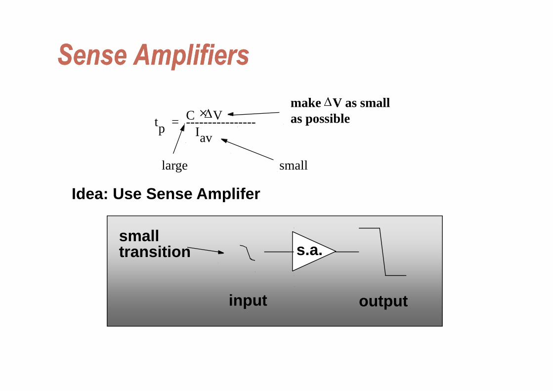
Sense AmplifiersSense AmplifiersSense AmplifiersSense Amplifiersmake ΔV as small
tpC ΔV×
Iav----------------=
make V as smallas possible
smalllarge
Idea: Use Sense AmpliferIdea: Use Sense Amplifer
smalls.a.
smalltransition
outputinput
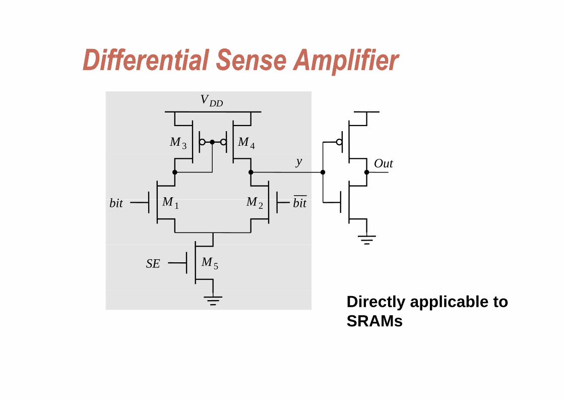
Differential Sense AmplifierDifferential Sense AmplifierDifferential Sense AmplifierDifferential Sense AmplifierVDD
M 4M 3
M M bibi
Outy
M 1 M 2 bitbit
M 5SE
Directly applicable toSRAMs
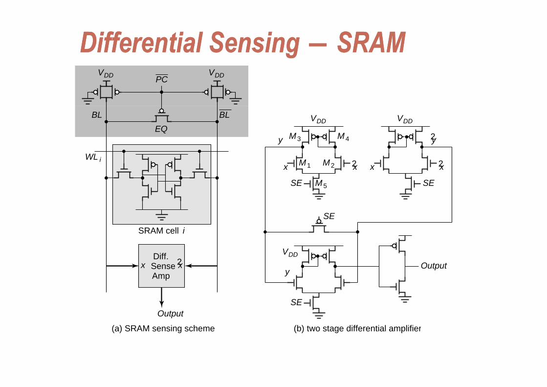
Differential Sensing ― SRAMDifferential Sensing ― SRAMVDD VDDPC
VDDBL
EQVDD
BL
M3 M4y 2y
WL i M1
M5
M2x
SE SE
x2x 2x
SRAM cell i
SE
VDDDiff.SenseAmp
2xx Outputy
( ) SRAM i h (b) t t diff ti l lifi
OutputSE
(a) SRAM sensing scheme (b) two stage differential amplifier
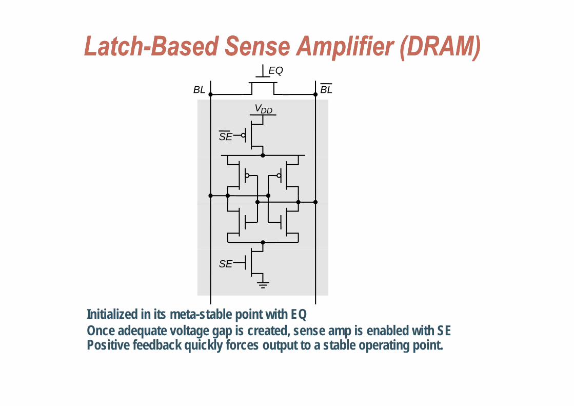
LatchLatch--Based Sense Amplifier (DRAM)Based Sense Amplifier (DRAM)EQ
VDD
BL BL
VDD
SE
SE
Initialized in its meta-stable point with EQOnce adequate voltage gap is created, sense amp is enabled with SEP iti f db k i kl f t t t t bl ti i tPositive feedback quickly forces output to a stable operating point.
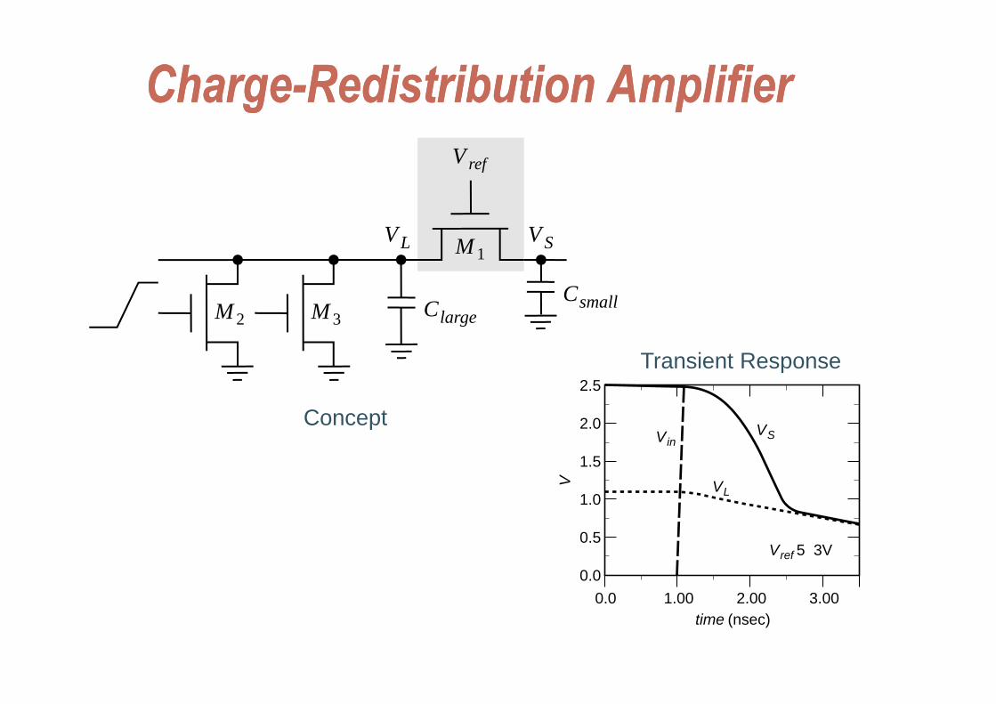
ChargeCharge--Redistribution AmplifierRedistribution AmplifierggVref
M 1VL VS
M 2 M 3CsmallClarge
2.0
2.5
V VSConcept
Transient Response
1.0
1.5
V
Vin
VL
VS
0.5
0.0Vref 5 3V
0.0 1.00 2.00time (nsec)
3.00
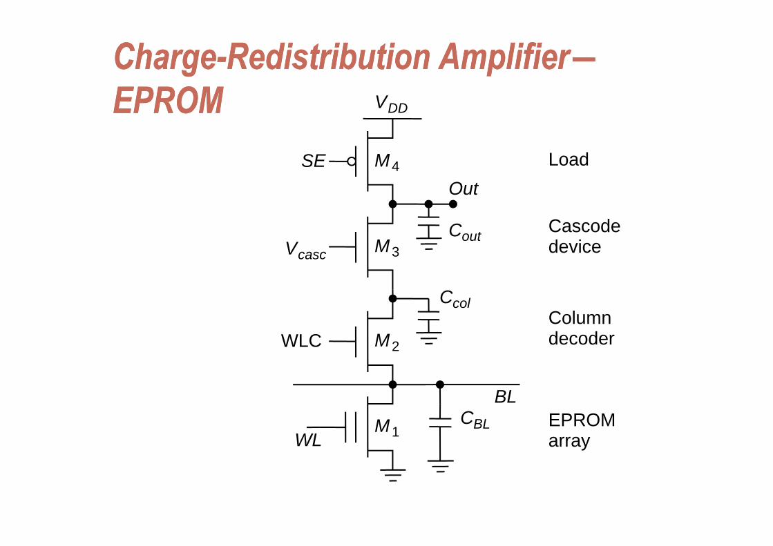
ChargeCharge--Redistribution Amplifier―Redistribution Amplifier―EPROMEPROMEPROMEPROM VDD
SE LoadOut
M4
CascodedeviceVcasc
CoutM3
WLCColumndecoder
Ccol
MWLC decoder
BL
M2
EPROMarray
BL
WLCBLM1
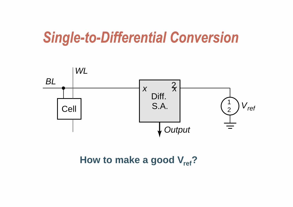
Si lSi l tt Diff ti l C iDiff ti l C iSingleSingle--toto--Differential ConversionDifferential Conversion
WLBL
Diff.S A
2xx
V
BL
1S.A.Cell
O t t
Vref12
Output
How to make a good Vref?
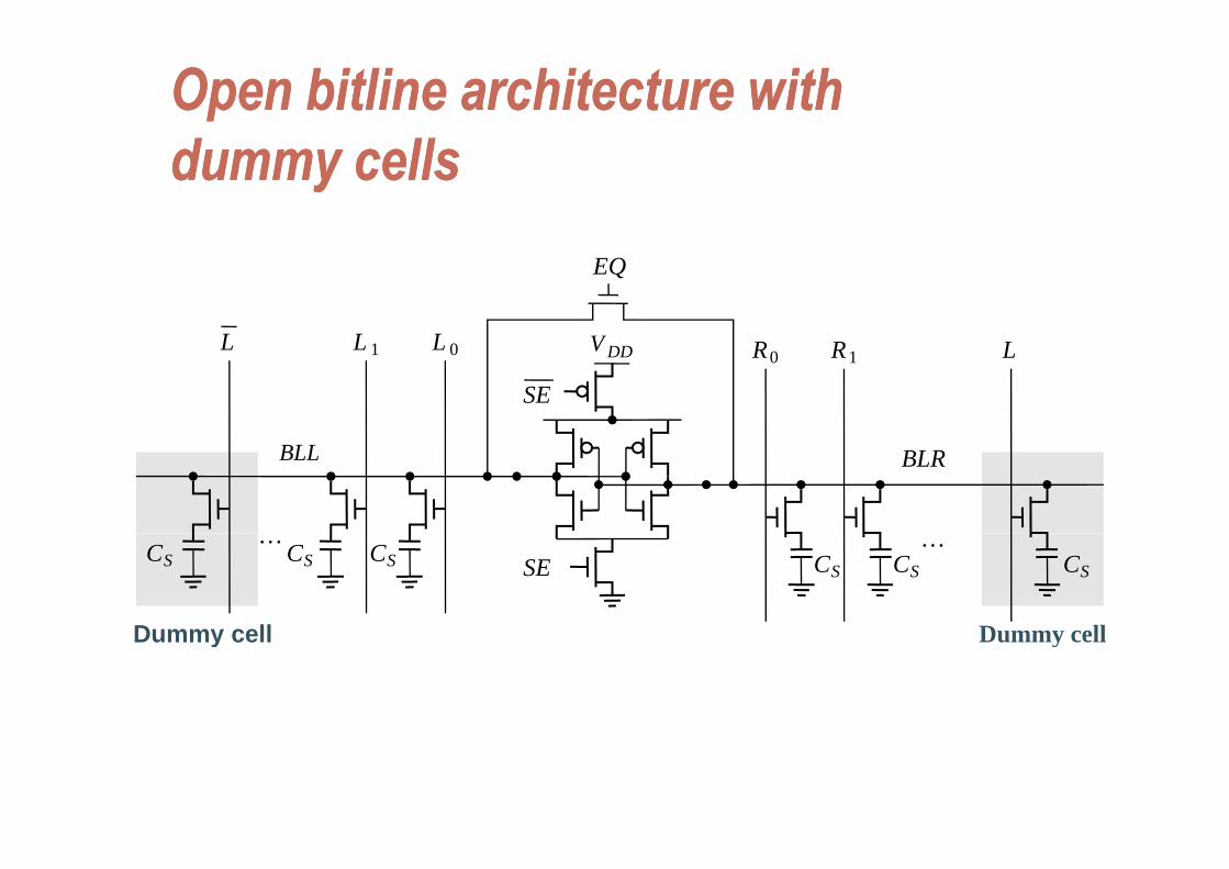
Open bitline architecture with Open bitline architecture with d lld lldummy cellsdummy cells
L L L V
EQ
L L 1 L 0 R0 R1 LV DD
SE
BLL BLR
CS CS CS CS CS CS
… …SE
Dummy cell Dummy cellDummy cell Dummy cell
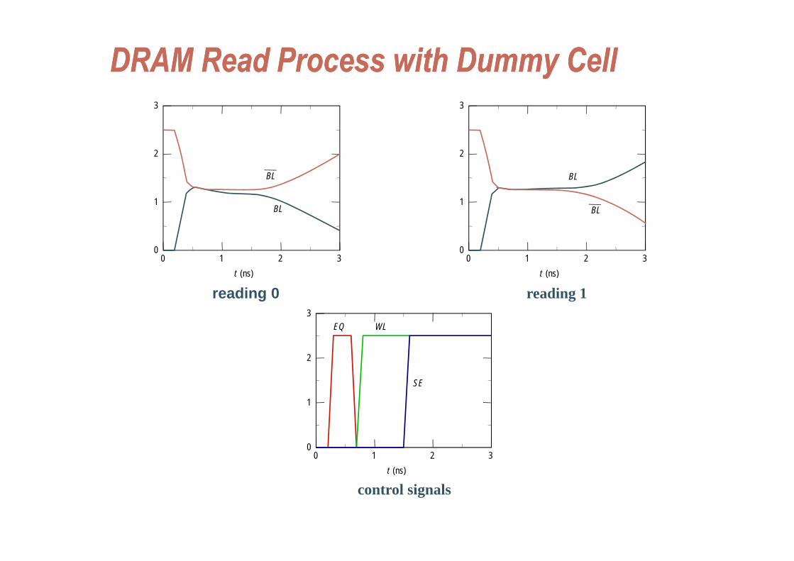
DRAM Read Process with Dummy CellDRAM Read Process with Dummy Cell3
2
3
22
1BL
BL
2
1
BL
BL
00 1 2 3
t (ns)
00 1 2 3
t (ns)
reading 03
EQ WL
reading 1
2
1
SE
00 1 2 3
t (ns)t (ns)
control signals
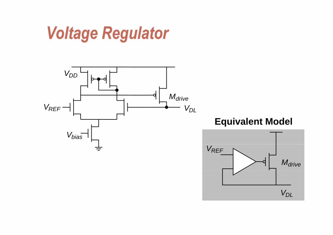
Voltage RegulatorVoltage RegulatorVoltage RegulatorVoltage Regulator
VDD
VREF
Mdrive
VDL
Vbias
Equivalent Model
-
+Mdrive
VREF
VDL
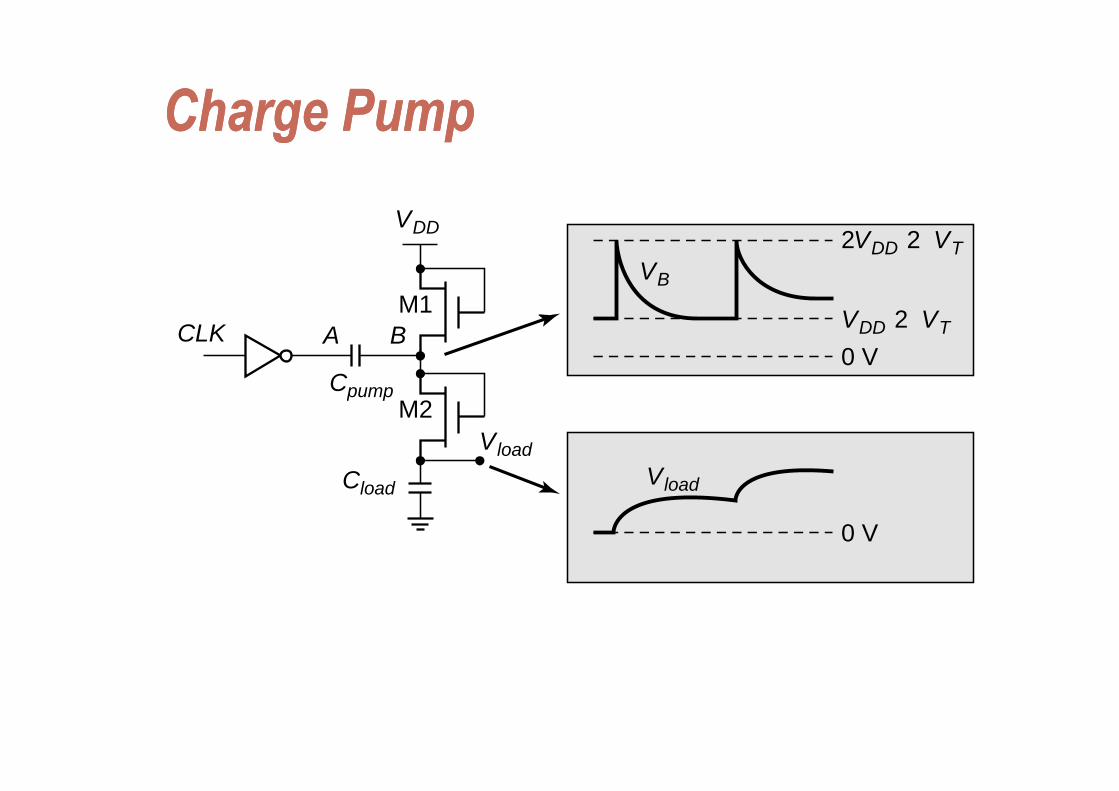
Charge PumpCharge PumpCharge PumpCharge PumpVVDD
M1
2VDD 2 VTVB
CLK A BM1
Cpump
VDD 2 VT
0 V
M2Vload
Cload
pump
VloadCload load
0 V
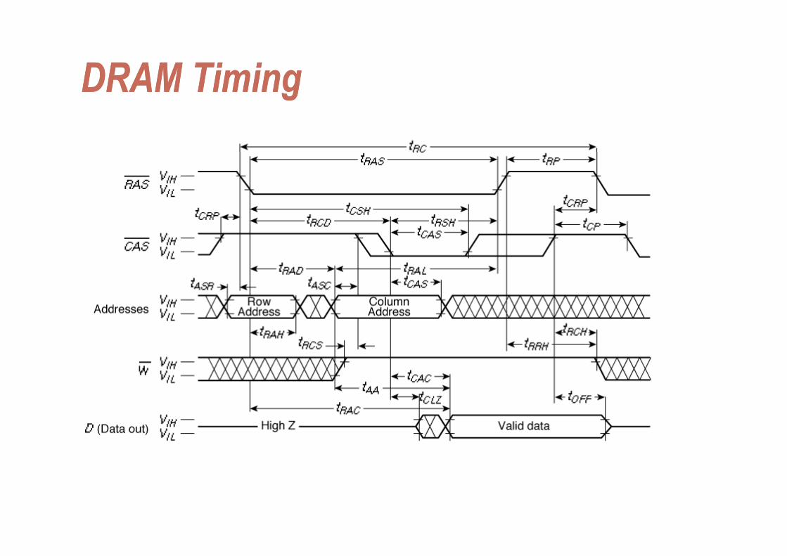
DRAM TimingDRAM TimingDRAM TimingDRAM Timing
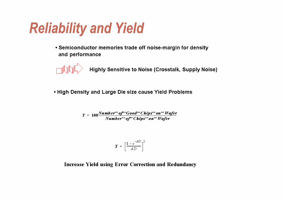
Reliability and YieldReliability and YieldReliability and YieldReliability and Yield
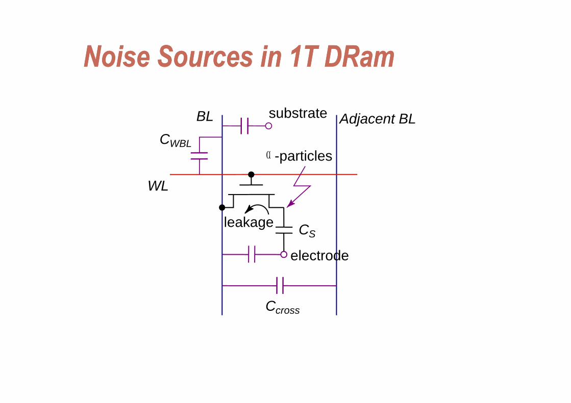
Noise Sources in 1T DRamNoise Sources in 1T DRamNoise Sources in 1T DRamNoise Sources in 1T DRamb t t
a particles
BL substrate Adjacent BLCWBL
a -particles
WL
leakage CS
electrode
Ccross
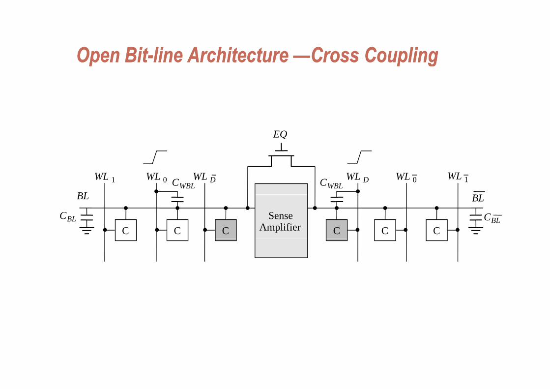
Open BitOpen Bit--line Architecture line Architecture ——Cross CouplingCross CouplingOpen BitOpen Bit line Architecture line Architecture Cross CouplingCross Coupling
EQ
WL 1
BLCWBL CWBL
WL 0 WL D WL D WL 0 WL 1
BL
SenseAmplifierC
BL
CBLCC C
CBLC C
BL
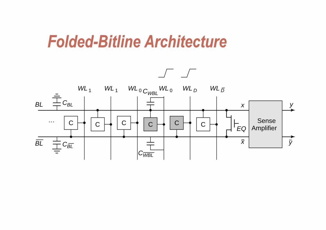
F ld dF ld d Bitli A hit tBitli A hit tFoldedFolded--Bitline ArchitectureBitline Architecture
WL 1 CWL 0 WL 0 WL DWL 1 WL DWL 1 CWBLWL 0 WL 0 WL DWL 1 WL D
BL CBL x y
SenseAmplifier
C C CC CC
BL
EQ
x y
…
CWBL
BL CBLx y
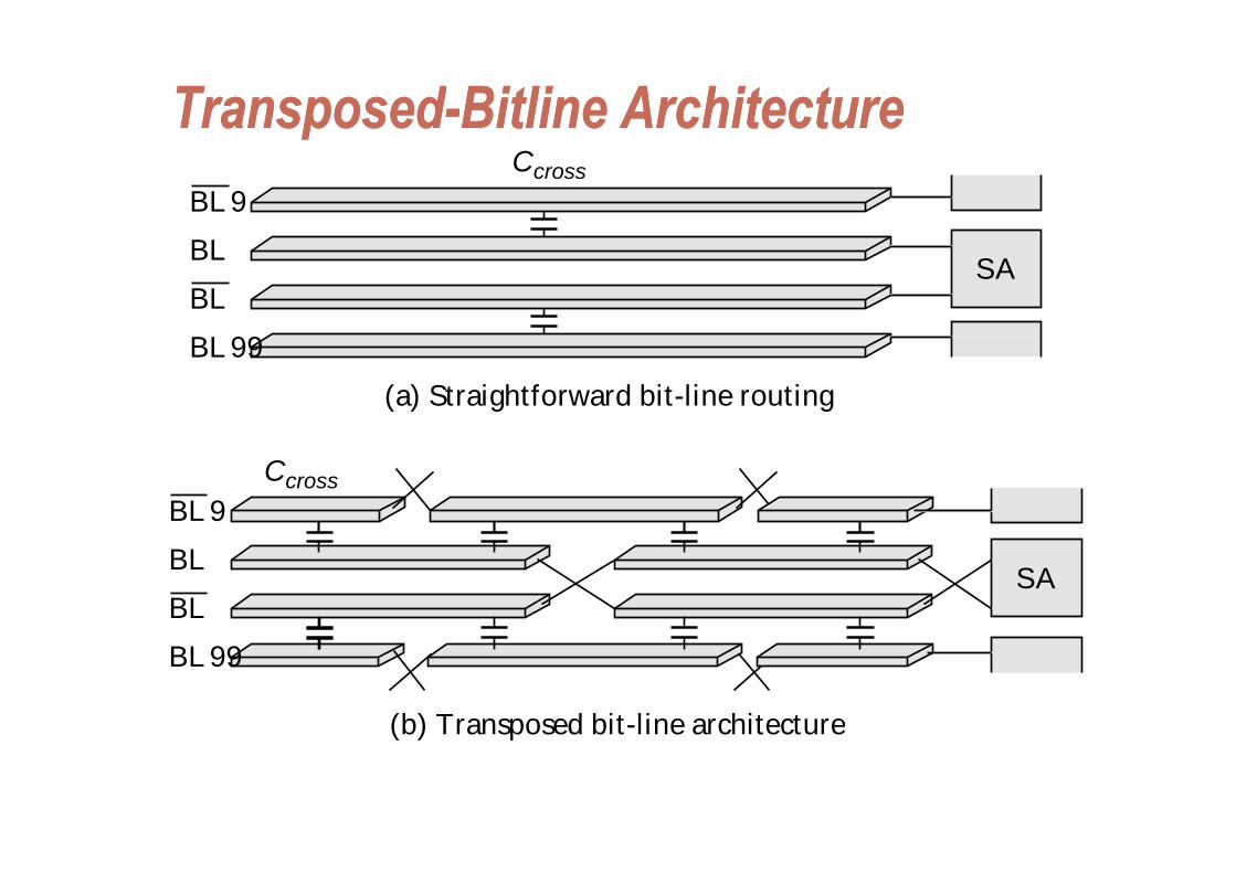
TransposedTransposed--Bitline ArchitectureBitline ArchitectureppCcross
BL 9
SABLBL
BL 99(a) Straightforward bit-line routing
BL 99
CcrossBL 9
SABLBL
(b) Transposed bit-line architecture
BL 99
(b) Transposed bit line architecture
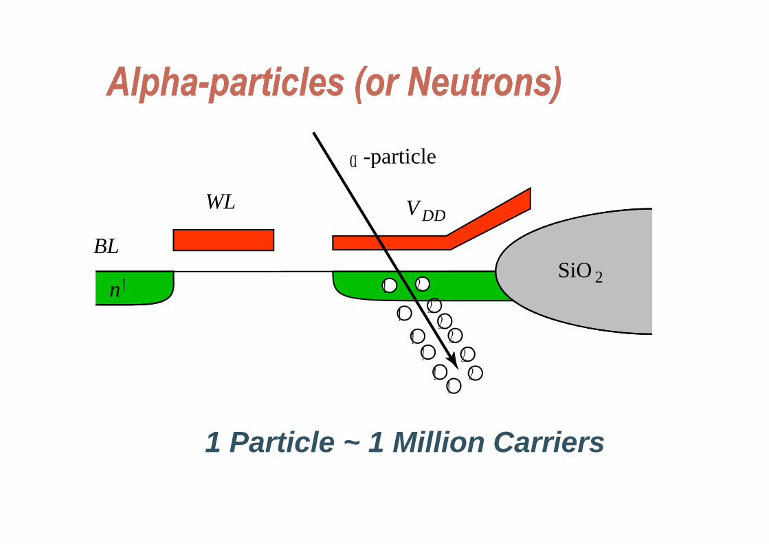
AlphaAlpha--particles (or Neutrons)particles (or Neutrons)AlphaAlpha--particles (or Neutrons)particles (or Neutrons)i l
WL V DD
a -particle
BL
V DD
SiO 2n 1SiO 2
1
11 2
22
2
1111
22
2
1 Particle ~ 1 Million Carriers
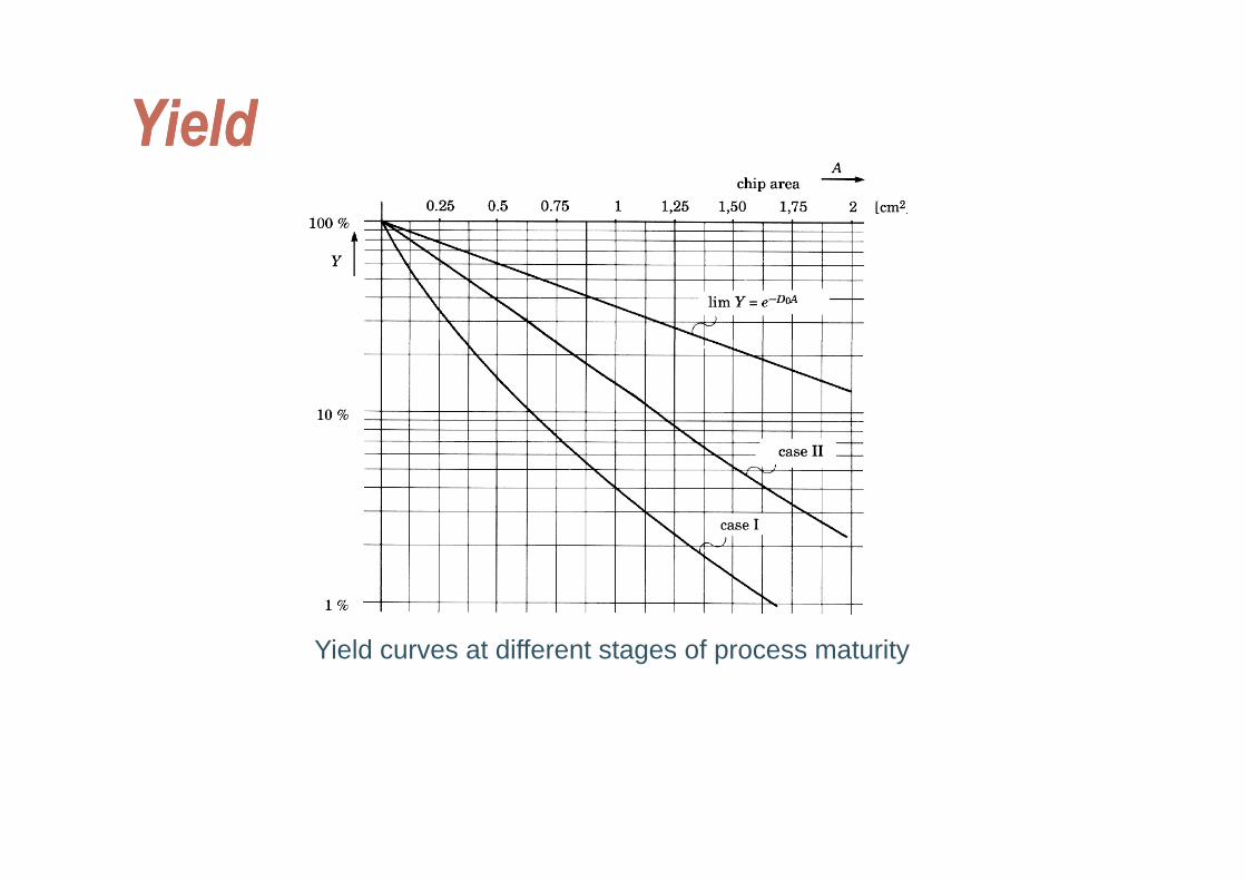
YieldYieldYieldYield
Yi ld t diff t t f t itYield curves at different stages of process maturity
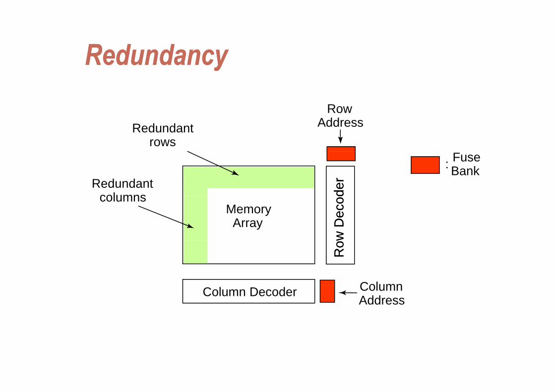
RedundancyRedundancyRedundancyRedundancyRow
Redundantrows
RowAddress
Redundantcolumns
FuseBank:
der
der
MemoryArray
columns
w
w DD
ecod
ecod
Column
Row
Row
Column Decoder ColumnAddress
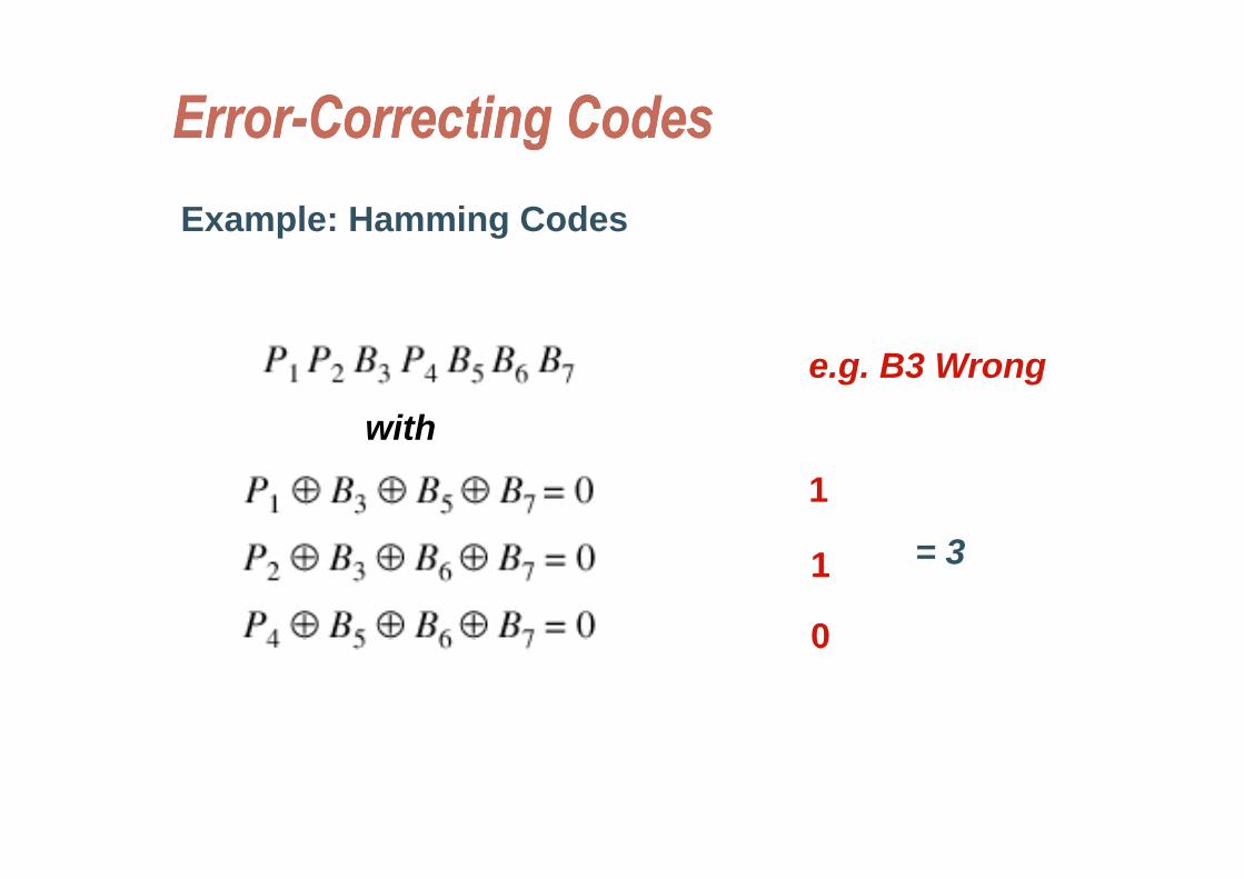
ErrorError--Correcting CodesCorrecting CodesggExample: Hamming Codes
with
e.g. B3 Wrong
with
1
31
0
= 3
0
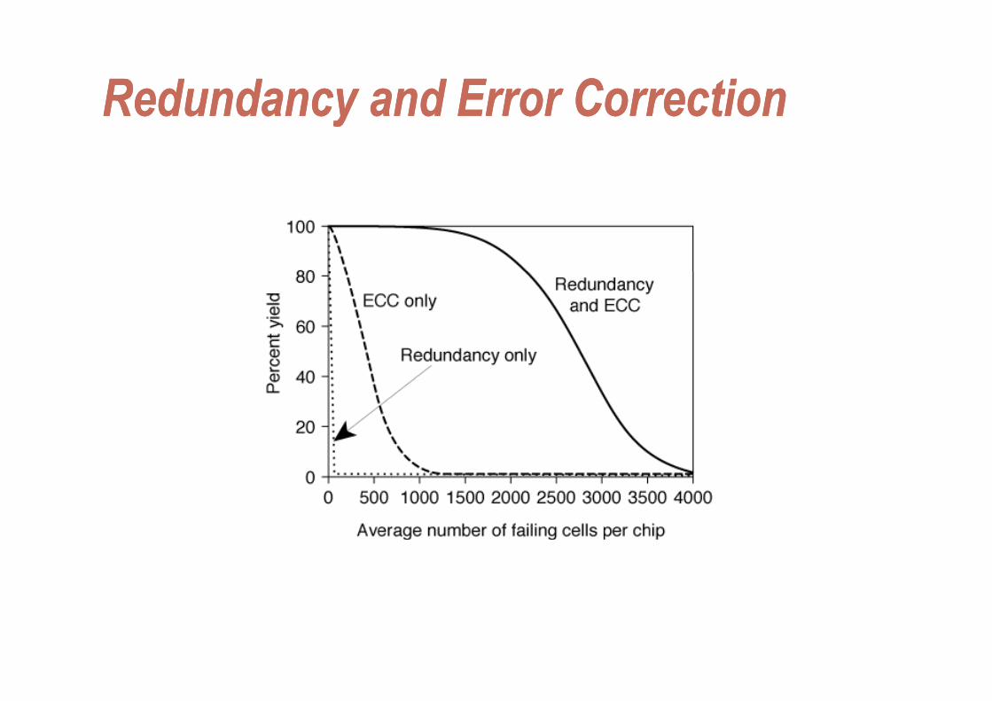
Redundancy and Error CorrectionRedundancy and Error CorrectionRedundancy and Error CorrectionRedundancy and Error Correction
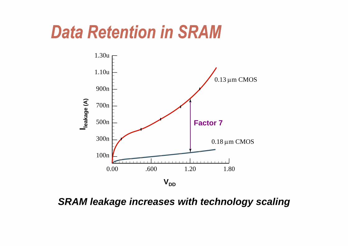
Data Retention in SRAMData Retention in SRAM1.30u
1.10u
900n0.13 μm CMOS
700n
500n Factor 7akag
e(A
)
500n
300n
Factor 7
0.18 μm CMOS
I le
100n
0.00 .600 1.20 1.80
VDD
SRAM leakage increases with technology scalingg gy g
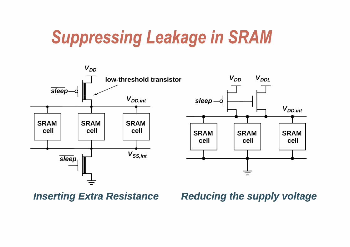
Suppressing Leakage in SRAMSuppressing Leakage in SRAMSuppressing Leakage in SRAMSuppressing Leakage in SRAMVVDD
VDD VDDL
sleeplow-threshold transistor
SRAM SRAM SRAM
VDD,intVDD,int
sleep
SRAMcell
SRAMcell
SRAMcell
V
SRAMcell
SRAMcell
SRAMcell
VSS,intsleep
Reducing the supply voltageReducing the supply voltageInserting Extra ResistanceInserting Extra Resistance
ConclusionsConclusionsConclusionsConclusionsThe field of memory design is a dynamic andThe field of memory design is a dynamic and exciting specialty:
Coordinated efforts from marketing and planningCoordinated efforts from marketing and planning, process design, device design, circuit design, test & production engineering, and software& production engineering, and software engineering are all needed.Many innovative approaches are possible in every y pp p ydesign stage. The market competition is fierce, but the winner is awarded with a big prize.The leading memory technologies are being pioneered by domestic companies/engineers.

ConclusionsConclusionsConclusionsConclusionsThink flexible and think “big ”Think flexible and think big.
Succeed as an engineer.gsElf-Motivated
eNergetic
EngineerEngineer ==
Self-manaGed
Insightful
iNnovativeiNnovative
Eye on data
Executexecute
Rewards


![Molecular Wires, Switches and Memories · devices, and memories. Molecular electronics [1-3] is conceptually different from conventional solid state semiconductor electronics. It](https://img.pdfslide.net/doc/110x75/5ecb1229c78cbc769f459166/molecular-wires-switches-and-memories-devices-and-memories-molecular-electronics.jpg)