Embed Size (px)
Citation preview
1
Compact Ultra-Wideband Bandpass and
Notched Bandpass Filter Using Dual-Line
Coupling Structure
E8-242: Radio Frequency Integrated Circuits & Systems
Mini Project Report By,
Amanulla Khan
M.Tech, CEDT
IISc, Bangalore
2
Abstract:
This report presents a compact ultra-wideband (UWB) microstrip bandpass filter and a notched
bandpass filter with spurious response suppression. A dual-mode ring resonator is constituted to
allocate its first two resonant frequencies in the UWB band, and the dual-line parallel-coupled
structure is used in this compact UWB filter, which achieves much tighter coupling degree. For
the notched filter, λ/4 open circuited stubs provide a sharp stopband at HyperLAN frequency of
5.2 GHz. Simulated and measured results are found in good agreement with each other. For the
bandpass filter, we have a wide passband from 3.9 to 10.8 GHz, fractional bandwidth of
101.825%, -10 dB return loss bandwidth of about 5 GHz, minimum insertion loss of 0.01 dB at
6.34 GHz. For the notched bandpass filter, we have 1st passband of 3.9 to 4.95 GHz, a notch of
bandwidth 4.95 to 5.9 GHz, and the 2nd
passband from 5.9 to 10.8 GHz. It has 26 dB return loss
at 5.2 GHz, minimum insertion loss of 0.1 at 7.75 GHz.
1. Introduction:
In 2002, the Federal Communications Commission (FCC) of the United States released the
frequency band 3.1-10.6 GHz for ultra-wideband (UWB) commercial communications. So
recently, more attention has been paid to applications of ultra-wideband (UWB) technology on
wireless communication system. UWB technology is promising and attractive for local area
networks, position location and tracking, and radar systems, because UWB has the
characteristics of low cost, high data transmission rate and very low power consumption. Many
UWB devices and circuits have been proposed and investigated widely. It is important to reduce
their size and weight in order to integrate them with other components as a compact system.
Compact and broadband bandpass filter (BPF) is a key passive component and highly demanded
in a UWB system. A planar BPF, based on a microstrip structure, can provide the advantages of
easy design, low cost, compact size, and is widely used in a variety of RF/microwave and
millimeter-wave systems to transmit energy in passband and to attenuate energy in one or more
stopbands. So, compact UWB microstrip BPF can be used in a UWB communication system.
UWB filters must have a fractional bandwidth of more than 70%, and it is very difficult to
achieve such a wide passband with a traditional parallel-coupled transmission line structure.
Therefore, there is a requirement for UWB BPF with a strong coupling structure that can be
3
easily fabricated. In this design, a dual-line coupling structure has been used to implement a
strong coupling between the input/output port and the resonator, which is more compact than the
inter-digital coupling structure. A compact UWB microstrip BPF and Notched BPF with low
insertion loss have been presented and analyzed. In addition, the UWB filters have extremely
compact size of 25 mm X 10 mm for BPF and 25 mm X 28 mm for Notched BPF when the
length of the feed lines is ignored.
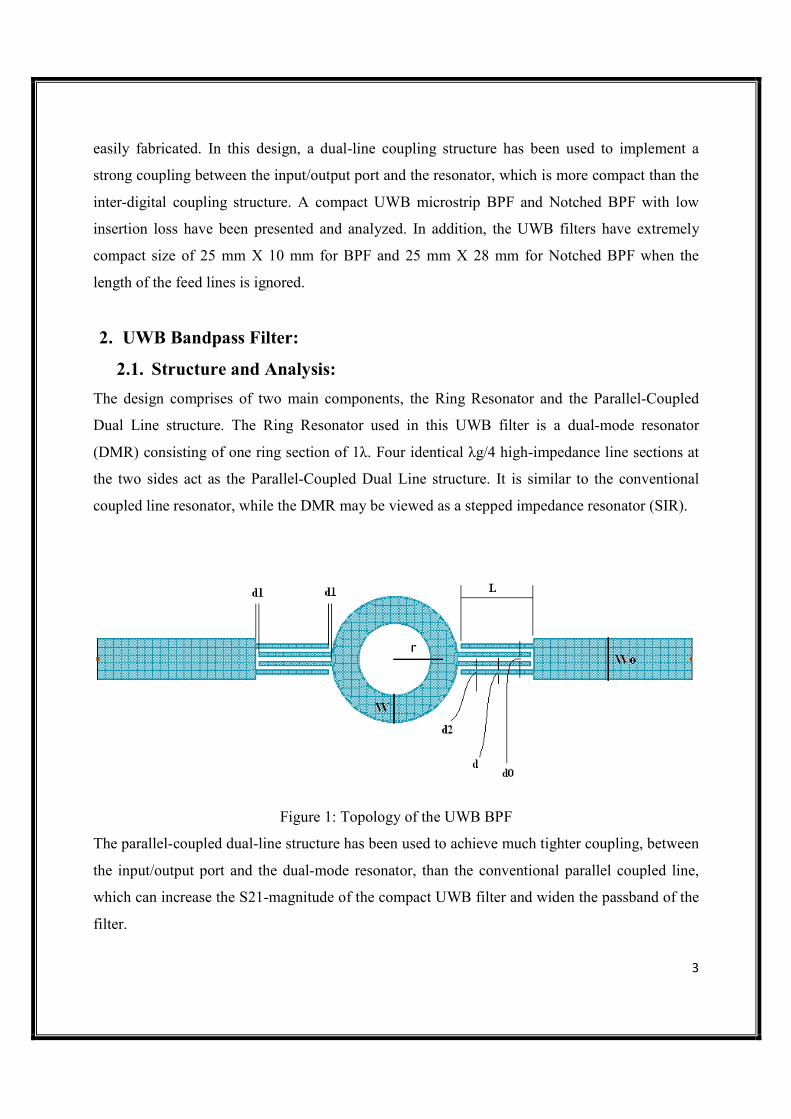
2. UWB Bandpass Filter:
2.1. Structure and Analysis:
The design comprises of two main components, the Ring Resonator and the Parallel-Coupled
Dual Line structure. The Ring Resonator used in this UWB filter is a dual-mode resonator
(DMR) consisting of one ring section of 1λ. Four identical λg/4 high-impedance line sections at
the two sides act as the Parallel-Coupled Dual Line structure. It is similar to the conventional
coupled line resonator, while the DMR may be viewed as a stepped impedance resonator (SIR).
Figure 1: Topology of the UWB BPF
The parallel-coupled dual-line structure has been used to achieve much tighter coupling, between
the input/output port and the dual-mode resonator, than the conventional parallel coupled line,
which can increase the S21-magnitude of the compact UWB filter and widen the passband of the
filter.
4
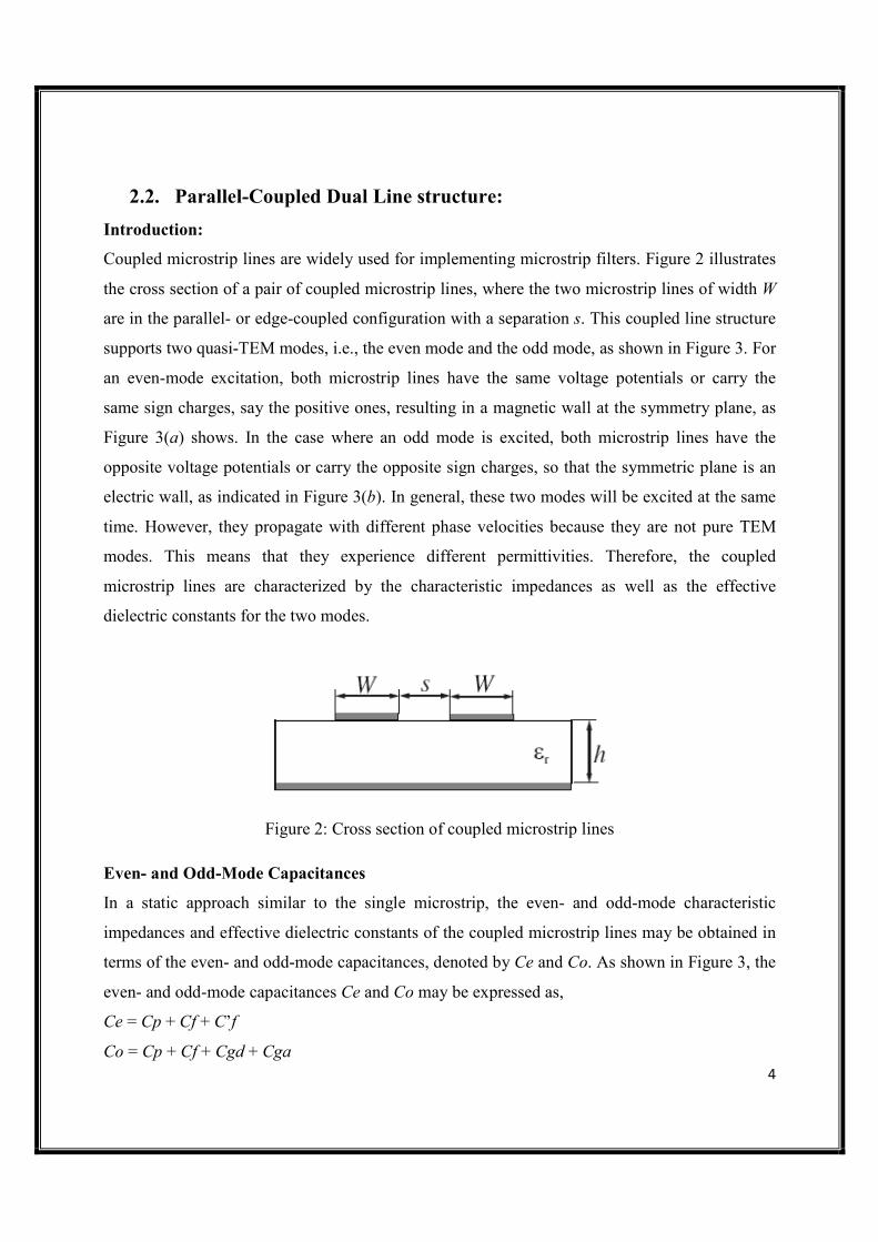
2.2. Parallel-Coupled Dual Line structure:
Introduction:
Coupled microstrip lines are widely used for implementing microstrip filters. Figure 2 illustrates
the cross section of a pair of coupled microstrip lines, where the two microstrip lines of width W
are in the parallel- or edge-coupled configuration with a separation s. This coupled line structure
supports two quasi-TEM modes, i.e., the even mode and the odd mode, as shown in Figure 3. For
an even-mode excitation, both microstrip lines have the same voltage potentials or carry the
same sign charges, say the positive ones, resulting in a magnetic wall at the symmetry plane, as
Figure 3(a) shows. In the case where an odd mode is excited, both microstrip lines have the
opposite voltage potentials or carry the opposite sign charges, so that the symmetric plane is an
electric wall, as indicated in Figure 3(b). In general, these two modes will be excited at the same
time. However, they propagate with different phase velocities because they are not pure TEM
modes. This means that they experience different permittivities. Therefore, the coupled
microstrip lines are characterized by the characteristic impedances as well as the effective
dielectric constants for the two modes.
Figure 2: Cross section of coupled microstrip lines
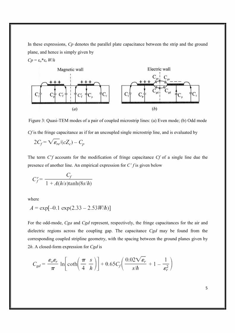
Even- and Odd-Mode Capacitances
In a static approach similar to the single microstrip, the even- and odd-mode characteristic
impedances and effective dielectric constants of the coupled microstrip lines may be obtained in
terms of the even- and odd-mode capacitances, denoted by Ce and Co. As shown in Figure 3, the
even- and odd-mode capacitances Ce and Co may be expressed as,
Ce = Cp + Cf + C’f
Co = Cp + Cf + Cgd + Cga
5
In these expressions, Cp denotes the parallel plate capacitance between the strip and the ground
plane, and hence is simply given by
Cp = εo*εr W/h
Figure 3: Quasi-TEM modes of a pair of coupled microstrip lines: (a) Even mode; (b) Odd mode
Cf is the fringe capacitance as if for an uncoupled single microstrip line, and is evaluated by
The term C’f accounts for the modification of fringe capacitance Cf of a single line due the
presence of another line. An empirical expression for C’ f is given below
where
For the odd-mode, Cga and Cgd represent, respectively, the fringe capacitances for the air and
dielectric regions across the coupling gap. The capacitance Cgd may be found from the
corresponding coupled stripline geometry, with the spacing between the ground planes given by
2h. A closed-form expression for Cgd is
6
The capacitance Cga can be modified from the capacitance of the corresponding coplanar strips,
and expressed in terms of a ratio of two elliptic functions
where
and the ratio of the elliptic functions is given by
The capacitances obtained by using above design equations [11] are found to be accurate to
within 3% over the ranges 0.2 <= W/h<= 2, 0.05 <= s/h <= 2, and ἐr>= 1.
Even- and Odd-Mode Characteristic Impedances and Effective Dielectric Constants
The even- and odd-mode characteristic impedances Zce and Zco can be obtained from the
capacitances. This analysis yields,
where Cae and Cao are even- and odd-mode capacitances for the coupled microstrip line
configuration with air as dielectric.
Effective dielectric constants εre and εro for even and odd modes, respectively, can be obtained
from Ce and Co by using the relations
7
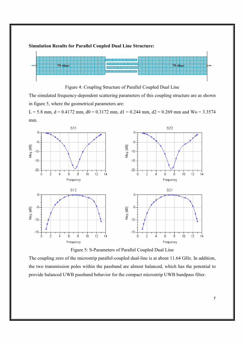
Simulation Results for Parallel Coupled Dual Line Structure:
Figure 4: Coupling Structure of Parallel Coupled Dual Line
The simulated frequency-dependent scattering parameters of this coupling structure are as shown
in figure 5, where the geometrical parameters are:
L = 5.8 mm, d = 0.4172 mm, d0 = 0.3172 mm, d1 = 0.244 mm, d2 = 0.269 mm and Wo = 3.3574
mm.
Figure 5: S-Parameters of Parallel Coupled Dual Line
The coupling zero of the microstrip parallel-coupled dual-line is at about 11.64 GHz. In addition,
the two transmission poles within the passband are almost balanced, which has the potential to
provide balanced UWB passband behavior for the compact microstrip UWB bandpass filter.
8
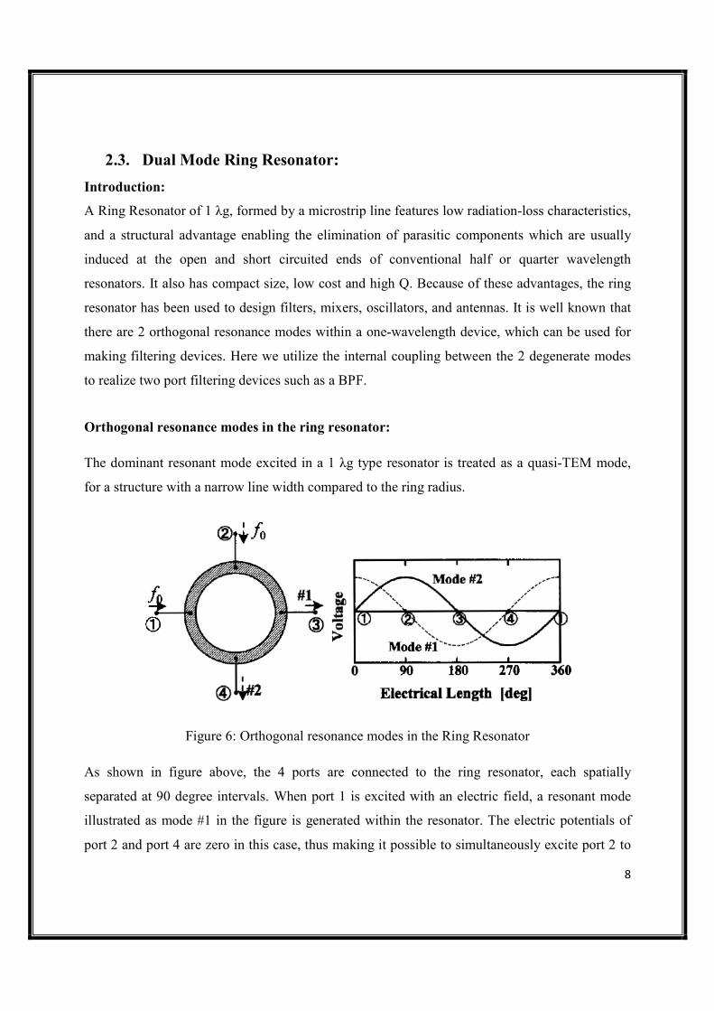
2.3. Dual Mode Ring Resonator:
Introduction:
A Ring Resonator of 1 λg, formed by a microstrip line features low radiation-loss characteristics,
and a structural advantage enabling the elimination of parasitic components which are usually
induced at the open and short circuited ends of conventional half or quarter wavelength
resonators. It also has compact size, low cost and high Q. Because of these advantages, the ring
resonator has been used to design filters, mixers, oscillators, and antennas. It is well known that
there are 2 orthogonal resonance modes within a one-wavelength device, which can be used for
making filtering devices. Here we utilize the internal coupling between the 2 degenerate modes
to realize two port filtering devices such as a BPF.
Orthogonal resonance modes in the ring resonator:
The dominant resonant mode excited in a 1 λg type resonator is treated as a quasi-TEM mode,
for a structure with a narrow line width compared to the ring radius.
Figure 6: Orthogonal resonance modes in the Ring Resonator
As shown in figure above, the 4 ports are connected to the ring resonator, each spatially
separated at 90 degree intervals. When port 1 is excited with an electric field, a resonant mode
illustrated as mode #1 in the figure is generated within the resonator. The electric potentials of
port 2 and port 4 are zero in this case, thus making it possible to simultaneously excite port 2 to
9
obtain a mode #2 resonance. The electric potentials of port 1 and port 3 become zero for this
mode, thus enabling two independent resonance modes to simultaneously exist in the ring
resonator. The above described phenomenon can be qualitatively be explained by the concept of
the travelling wave. The incident wave at port 1 generates clockwise and anti clockwise
travelling waves. These two reach port 3 in the same phase, while at ports 2 and 4, they
encounter opposite phase. Hence the incident wave at port 1 can propagate to port 3 while
disappearing at ports 2 and 4. In the same way, incident wave at port 2 can propagate to port 4
while disappearing at ports 1 and 3.
Analysis of 1λ Ring Resonator:
When the mean circumference of the ring resonator is equal to an integral multiple of a guided
wavelength, resonance is established. This may be expressed as
Where, r is the mean radius of the ring that equals the average of the outer and inner radii, λg is
the guided wavelength, and n is the mode number.
This relation is valid for the loose coupling case, as it does not take into account the coupling gap
effects. From this equation, the resonant frequencies for different modes can be calculated since
λg is frequency dependent. For the first mode, the maxima of field occur at the coupling gap
locations, and nulls occur 90° from the coupling gap locations.
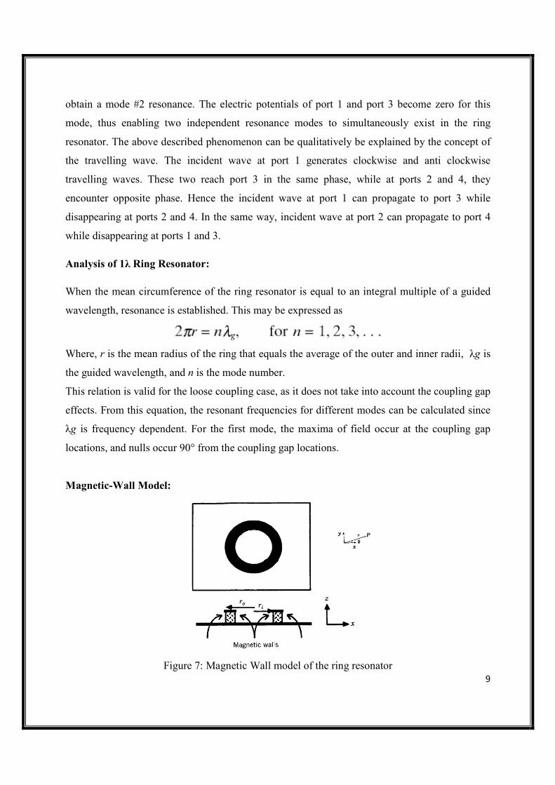
Magnetic-Wall Model:
Figure 7: Magnetic Wall model of the ring resonator
10
The magnetic-wall model considers the ring as a cavity resonator with electric walls on the top
and bottom and magnetic walls on the sides as shown in Figure 7. The electromagnetic fields are
considered to be confined to the dielectric volume between the perfectly conducting ground
plane and the ring conductor. It is assumed that there is no z-dependency (∂/∂z = 0) and that the
fields are transverse magnetic (TM) to z direction. A solution of Maxwell’s equations in
cylindrical coordinates is
where A and B are constants, k is the wave number, ω is the angular frequency,
Jn is a Bessel function of the first kind of order n, and �n is a Bessel function of the second kind
and order n. J’n and N’n are the derivatives of the Bessel functions with respect to the argument
(kr).
The boundary conditions to be applied are
were r0 and ri are the outer and inner radii of the ring, respectively. Application of the boundary
condition leads to the eigen value equation,
Where,
Given εo and εr, then above equation can be solved for k. By using given equations the resonant
frequency can be found.
11
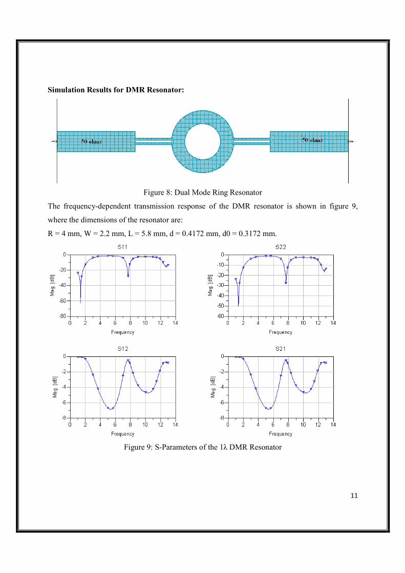
Simulation Results for DMR Resonator:
Figure 8: Dual Mode Ring Resonator
The frequency-dependent transmission response of the DMR resonator is shown in figure 9,
where the dimensions of the resonator are:
R = 4 mm, W = 2.2 mm, L = 5.8 mm, d = 0.4172 mm, d0 = 0.3172 mm.
Figure 9: S-Parameters of the 1λ DMR Resonator
12
The 1st resonant frequency of 7.635 GHz is in the interested UWB passband, and the 2
nd resonant
frequency of 12.47 GHz falls in the stop band of the UWB bandpass filter.
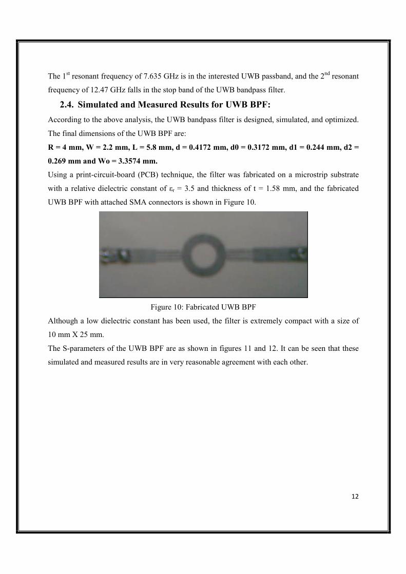
2.4. Simulated and Measured Results for UWB BPF:
According to the above analysis, the UWB bandpass filter is designed, simulated, and optimized.
The final dimensions of the UWB BPF are:
R = 4 mm, W = 2.2 mm, L = 5.8 mm, d = 0.4172 mm, d0 = 0.3172 mm, d1 = 0.244 mm, d2 =
0.269 mm and Wo = 3.3574 mm.
Using a print-circuit-board (PCB) technique, the filter was fabricated on a microstrip substrate
with a relative dielectric constant of εr = 3.5 and thickness of t = 1.58 mm, and the fabricated
UWB BPF with attached SMA connectors is shown in Figure 10.
Figure 10: Fabricated UWB BPF
Although a low dielectric constant has been used, the filter is extremely compact with a size of
10 mm X 25 mm.
The S-parameters of the UWB BPF are as shown in figures 11 and 12. It can be seen that these
simulated and measured results are in very reasonable agreement with each other.
13
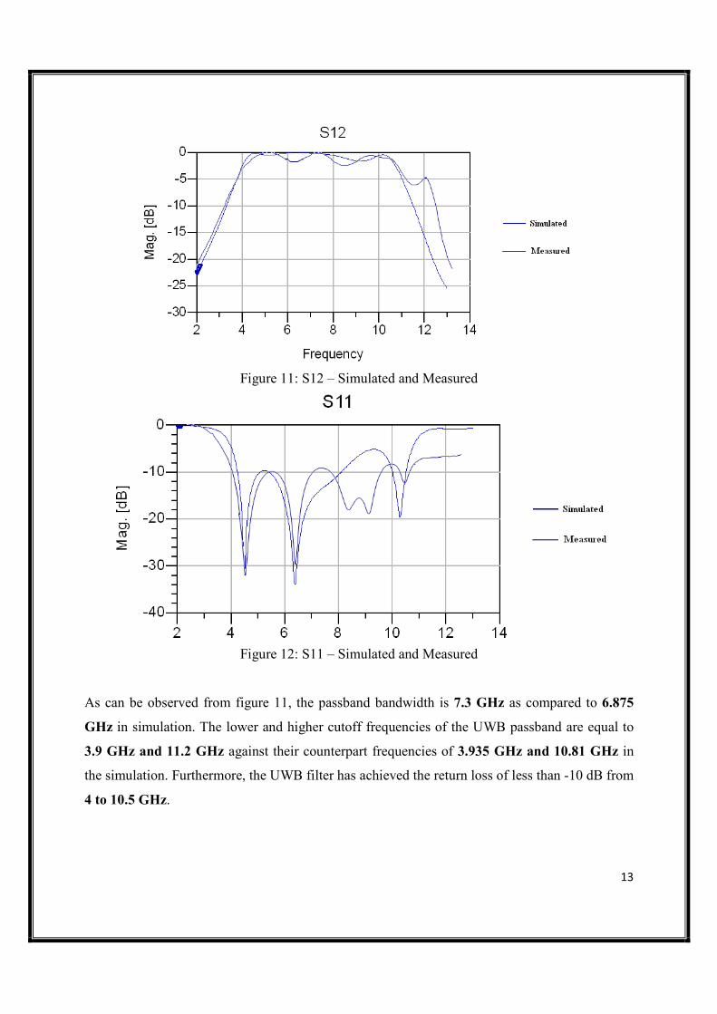
Figure 11: S12 – Simulated and Measured
Figure 12: S11 – Simulated and Measured
As can be observed from figure 11, the passband bandwidth is 7.3 GHz as compared to 6.875
GHz in simulation. The lower and higher cutoff frequencies of the UWB passband are equal to
3.9 GHz and 11.2 GHz against their counterpart frequencies of 3.935 GHz and 10.81 GHz in
the simulation. Furthermore, the UWB filter has achieved the return loss of less than -10 dB from
4 to 10.5 GHz.
14
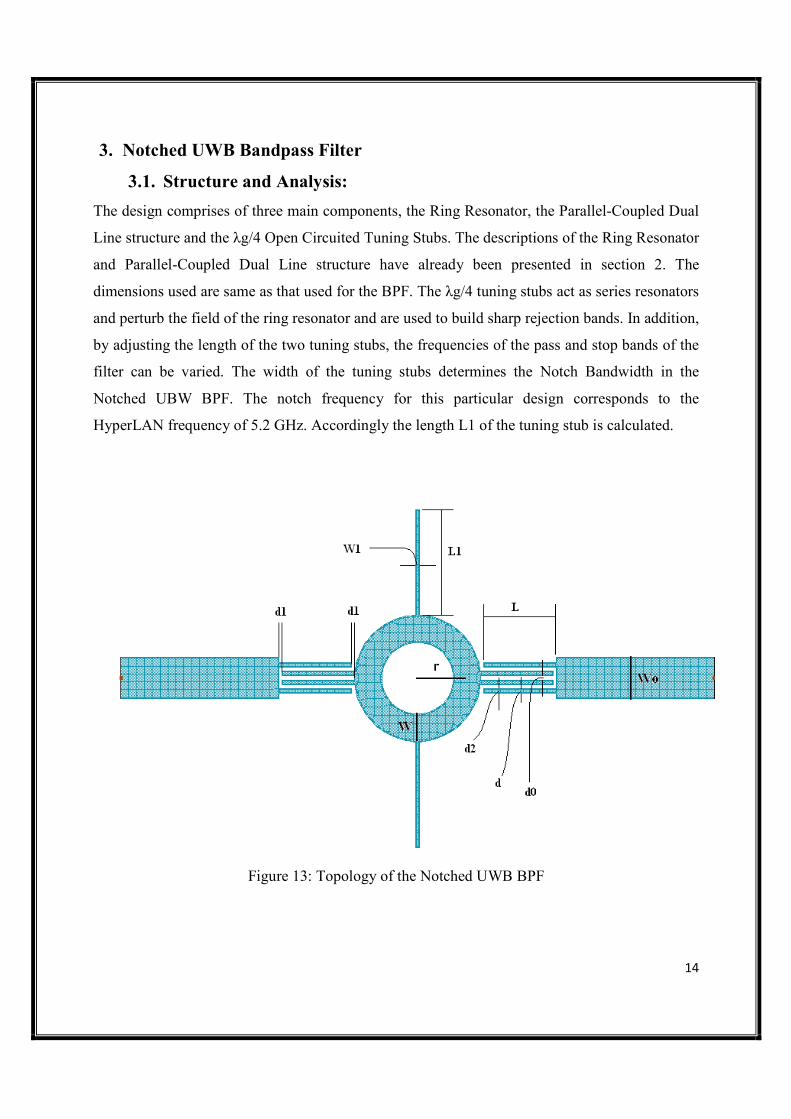
3. 8otched UWB Bandpass Filter
3.1. Structure and Analysis:
The design comprises of three main components, the Ring Resonator, the Parallel-Coupled Dual
Line structure and the λg/4 Open Circuited Tuning Stubs. The descriptions of the Ring Resonator
and Parallel-Coupled Dual Line structure have already been presented in section 2. The
dimensions used are same as that used for the BPF. The λg/4 tuning stubs act as series resonators
and perturb the field of the ring resonator and are used to build sharp rejection bands. In addition,
by adjusting the length of the two tuning stubs, the frequencies of the pass and stop bands of the
filter can be varied. The width of the tuning stubs determines the Notch Bandwidth in the
Notched UBW BPF. The notch frequency for this particular design corresponds to the
HyperLAN frequency of 5.2 GHz. Accordingly the length L1 of the tuning stub is calculated.
Figure 13: Topology of the Notched UWB BPF
15
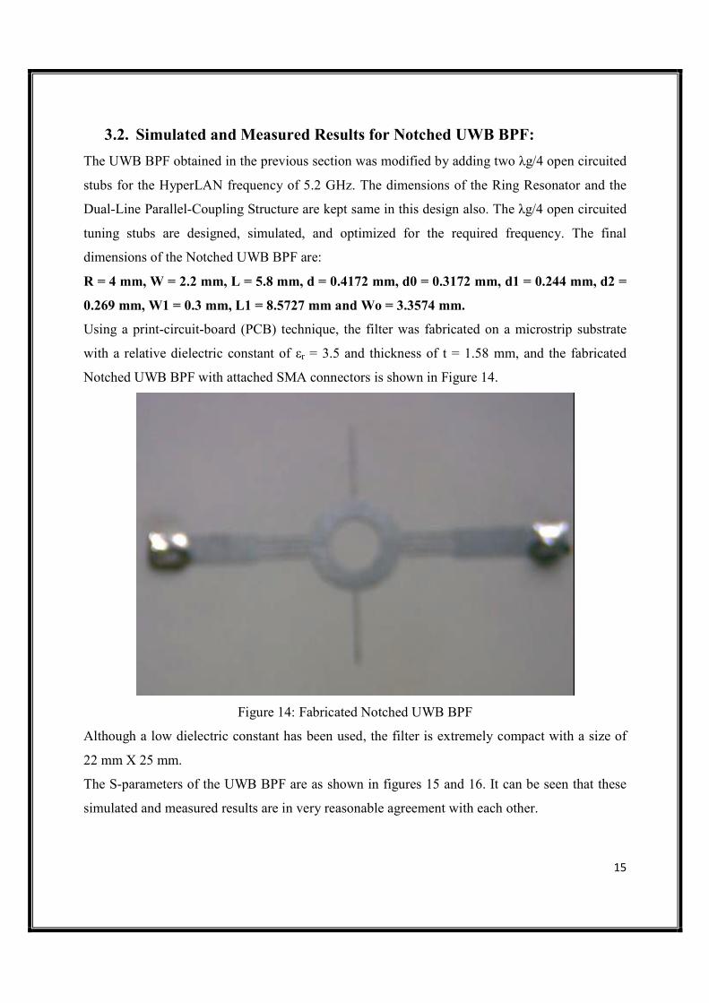
3.2. Simulated and Measured Results for 8otched UWB BPF:
The UWB BPF obtained in the previous section was modified by adding two λg/4 open circuited
stubs for the HyperLAN frequency of 5.2 GHz. The dimensions of the Ring Resonator and the
Dual-Line Parallel-Coupling Structure are kept same in this design also. The λg/4 open circuited
tuning stubs are designed, simulated, and optimized for the required frequency. The final
dimensions of the Notched UWB BPF are:
R = 4 mm, W = 2.2 mm, L = 5.8 mm, d = 0.4172 mm, d0 = 0.3172 mm, d1 = 0.244 mm, d2 =
0.269 mm, W1 = 0.3 mm, L1 = 8.5727 mm and Wo = 3.3574 mm.
Using a print-circuit-board (PCB) technique, the filter was fabricated on a microstrip substrate
with a relative dielectric constant of εr = 3.5 and thickness of t = 1.58 mm, and the fabricated
Notched UWB BPF with attached SMA connectors is shown in Figure 14.
Figure 14: Fabricated Notched UWB BPF
Although a low dielectric constant has been used, the filter is extremely compact with a size of
22 mm X 25 mm.
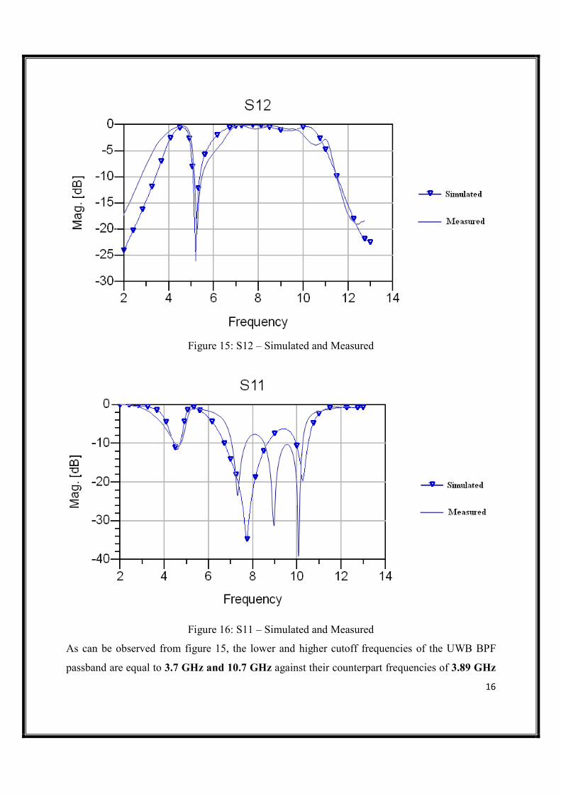
The S-parameters of the UWB BPF are as shown in figures 15 and 16. It can be seen that these
simulated and measured results are in very reasonable agreement with each other.
16
Figure 15: S12 – Simulated and Measured
Figure 16: S11 – Simulated and Measured
As can be observed from figure 15, the lower and higher cutoff frequencies of the UWB BPF
passband are equal to 3.7 GHz and 10.7 GHz against their counterpart frequencies of 3.89 GHz
17
and 10.81 GHz in the simulation. The notch frequency was found to be 5.27 GHz as compared
to 5.194 GHz in simulation. At the required frequency of 5.2 GHz, the attenuation was found to
be 16 dB. The notch was found to extend between 5.1 to 6.3 GHz as compared to 4.95 to 5.9
GHz obtained in simulation.
4. Conclusion
The compact UWB microstrip BPF and Notched BPF have been designed using the Dual-mode
Ring Resonator with the Parallel-coupled Dual-line structure. The Parallel-coupled Dual-line
structure has achieved much tighter coupling between the input/output port and the dual-mode
resonator than the conventional parallel coupled line. The compact UWB filters have been
fabricated, and tested. The fabricated UWB BPF has a 7.3 GHz passband, -10 dB return loss
bandwidth of 6.5 GHz. The fabricated Notched UWB BPF has a 7 GHz passband, 16 dB
attenuation at HyperLAN frequency of 5.2 GHz. These results have indicated a very good
agreement between simulation and measurements.
5. References
• “Compact Ultra-Wideband Bandpass Filter Using Dual-Line Coupling Structure” By
Kaijun Song and Yong Fan
• “Microwave Engineering” 3rd
Edition – D.M. Pozar
• “Microstrip Antenna Design Handbook” – Garg
• “Microstrip Filters for RF/Microwave Applications” - Jia-Sheng Hong & M. J. Lancaster
• “Microwave Resonators and Filters for Wireless Communication” – M. Makimoto &
S. Yamashita
• “A Novel Millimeter-Wave Ultra-Wideband Bandpass Filter Using Microstrip Dual-
Mode Ring Resonators Loaded with Open Tuning Stubs of Different Lengths” By
Zhewang Ma, Peng Cai, Xuehui Guan, Yoshio Kobayashi, Tetsuo Anada
• “Microwave Ring Circuits and Related Structures” - Kai Chang & Lung-Hwa Hsieh
• “Compact UWB bandpass filter with improved upper-stopband performance” By Q.-X. Chu and S.-T. Li
• Ultra-Wideband (UWB) Bandpass Filters Using Multiple-Mode Resonator Lei Zhu, Sheng Sun, Wolfgang Menzel
• “Aperture Compensation Technique For Innovative Design of Ultra-Broadband Microstrip Bandpass Filter” By Lei Zhu, Huuheng Bu, and Ke Wu