Embed Size (px)
Citation preview
1
2
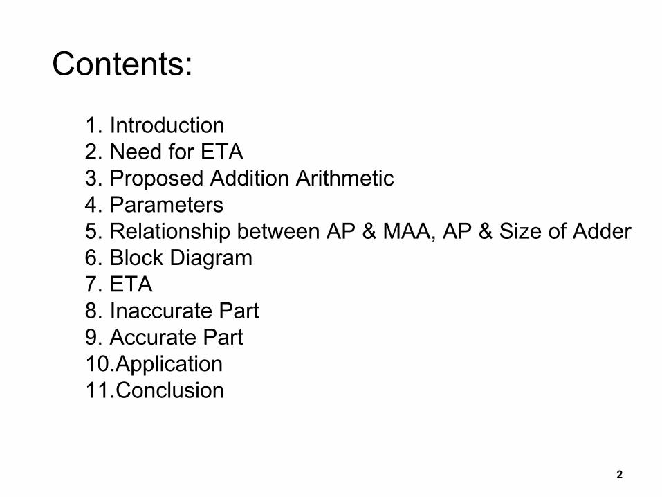
Contents:
1. Introduction2. Need for ETA3. Proposed Addition Arithmetic4. Parameters5. Relationship between AP & MAA, AP & Size of Adder6. Block Diagram7. ETA8. Inaccurate Part9. Accurate Part10.Application11.Conclusion
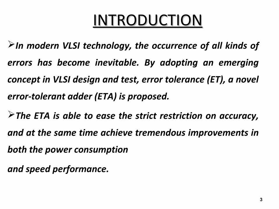
INTRODUCTIONINTRODUCTIONIn modern VLSI technology, the occurrence of all kinds of
errors has become inevitable. By adopting an emerging
concept in VLSI design and test, error tolerance (ET), a novel
error-tolerant adder (ETA) is proposed.
The ETA is able to ease the strict restriction on accuracy,
and at the same time achieve tremendous improvements in
both the power consumption
and speed performance.
3
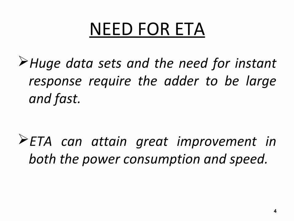
NEED FOR ETA
Huge data sets and the need for instant response require the adder to be large and fast.
ETA can attain great improvement in both the power consumption and speed.
4
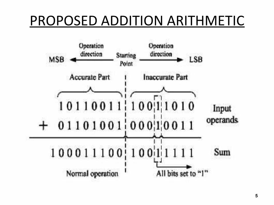
PROPOSED ADDITION ARITHMETIC
5
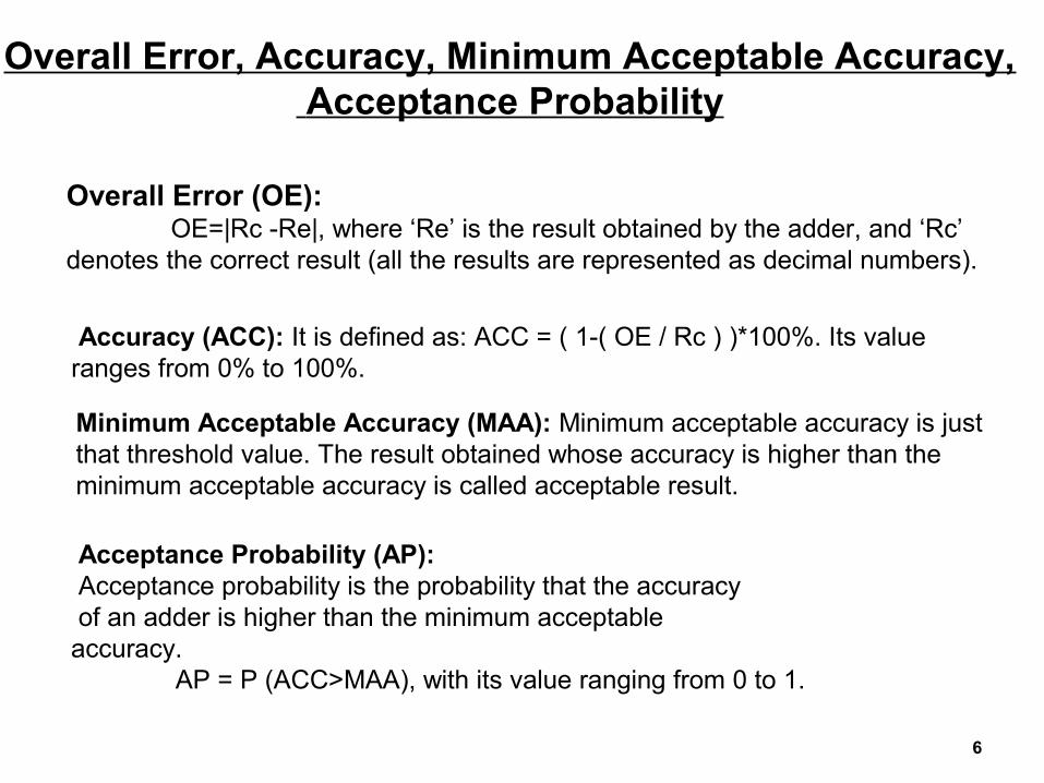
Overall Error, Accuracy, Minimum Acceptable Accuracy, Acceptance Probability
Overall Error (OE): OE=|Rc -Re|, where ‘Re’ is the result obtained by the adder, and ‘Rc’
denotes the correct result (all the results are represented as decimal numbers).
Accuracy (ACC): It is defined as: ACC = ( 1-( OE / Rc ) )*100%. Its value ranges from 0% to 100%.
Minimum Acceptable Accuracy (MAA): Minimum acceptable accuracy is just that threshold value. The result obtained whose accuracy is higher than the minimum acceptable accuracy is called acceptable result.
Acceptance Probability (AP): Acceptance probability is the probability that the accuracy of an adder is higher than the minimum acceptable accuracy.
AP = P (ACC>MAA), with its value ranging from 0 to 1.
6
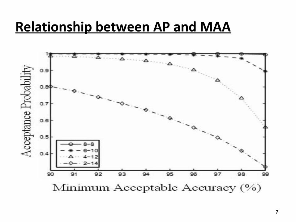
Relationship between AP and MAA
7
8
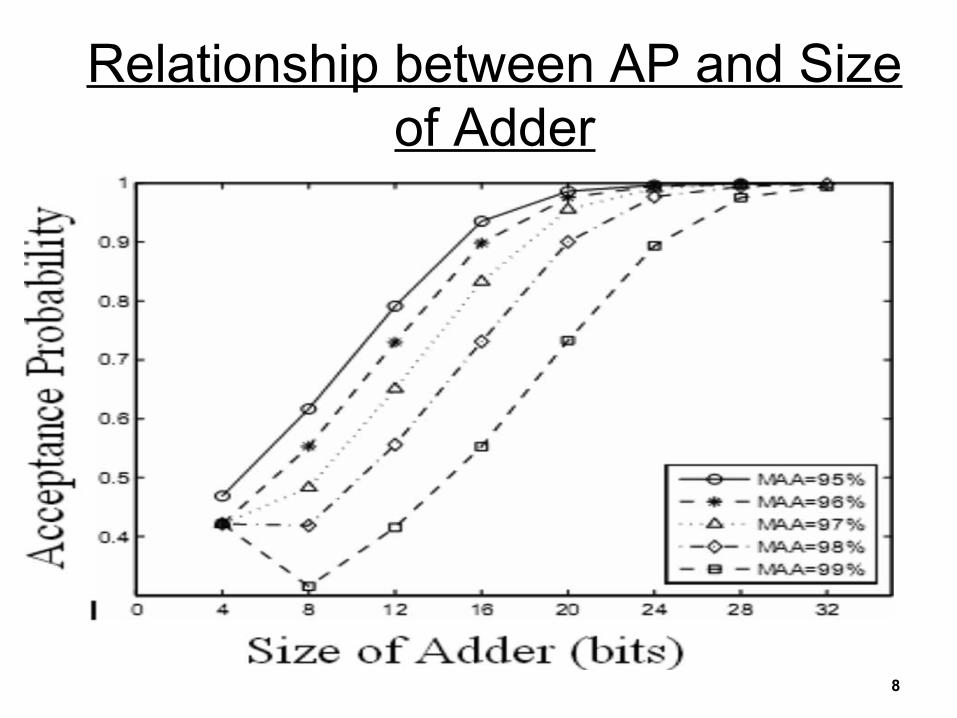
Relationship between AP and Size of Adder
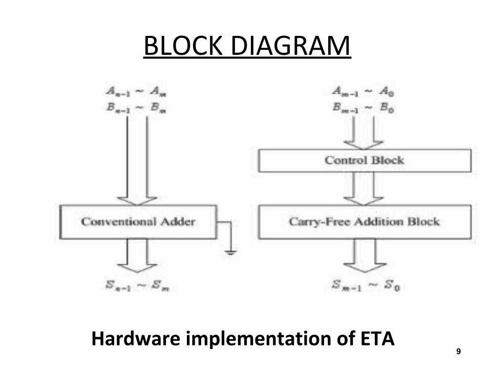
BLOCK DIAGRAM
Hardware implementation of ETA9
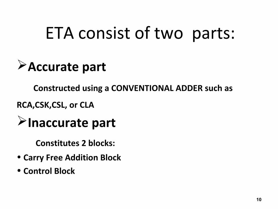
ETA consist of two parts:
Accurate part
Constructed using a CONVENTIONAL ADDER such as
RCA,CSK,CSL, or CLA
Inaccurate part Constitutes 2 blocks:
• Carry Free Addition Block• Control Block
10
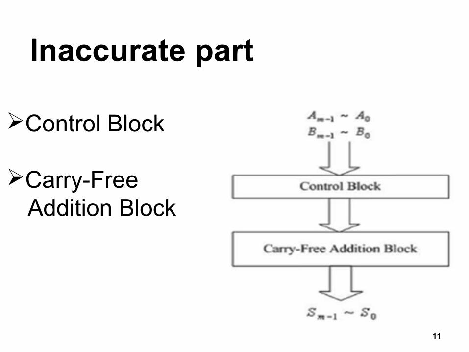
Inaccurate part :
Control Block
Carry-Free Addition Block
11
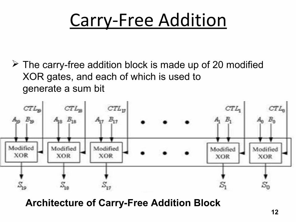
Carry-Free Addition
12Architecture of Carry-Free Addition Block
The carry-free addition block is made up of 20 modified XOR gates, and each of which is used to generate a sum bit
Carry-Free Addition
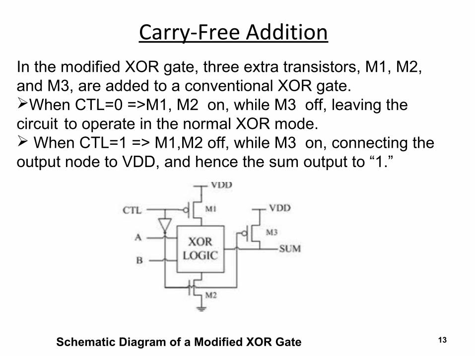
13Schematic Diagram of a Modified XOR Gate
In the modified XOR gate, three extra transistors, M1, M2, and M3, are added to a conventional XOR gate. When CTL=0 =>M1, M2 on, while M3 off, leaving the circuit to operate in the normal XOR mode. When CTL=1 => M1,M2 off, while M3 on, connecting the output node to VDD, and hence the sum output to “1.”
Control Block
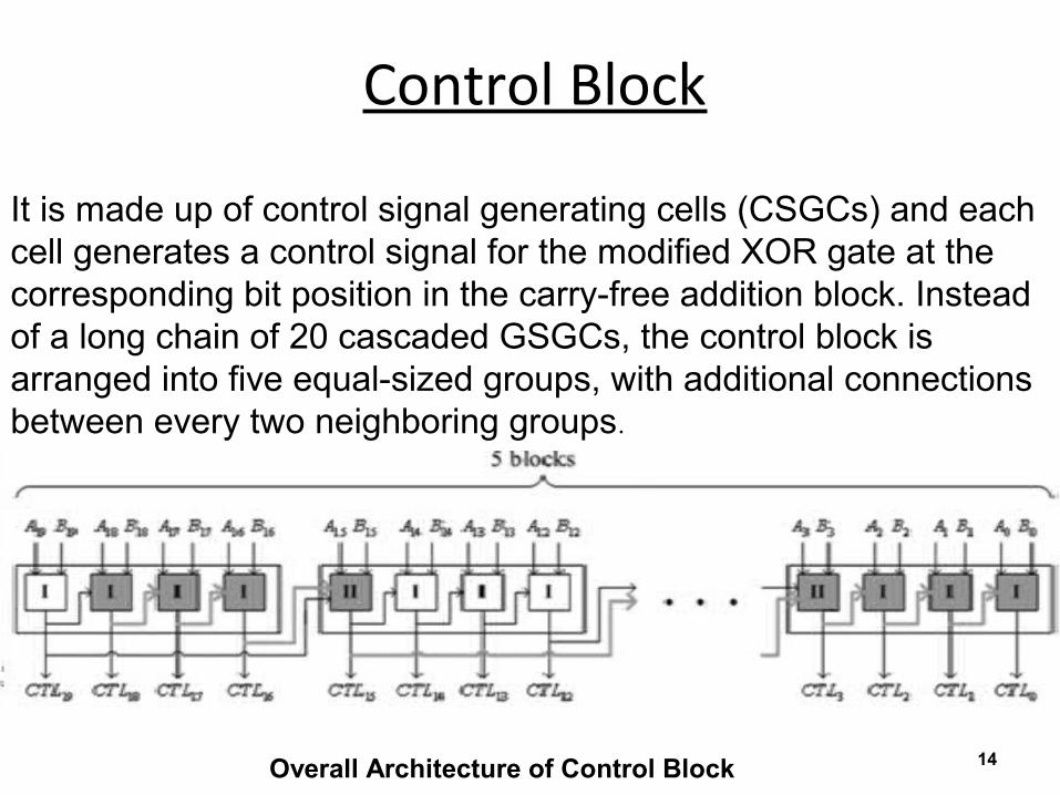
14Overall Architecture of Control Block
It is made up of control signal generating cells (CSGCs) and each cell generates a control signal for the modified XOR gate at the corresponding bit position in the carry-free addition block. Instead of a long chain of 20 cascaded GSGCs, the control block is arranged into five equal-sized groups, with additional connections between every two neighboring groups.
15
Control Block
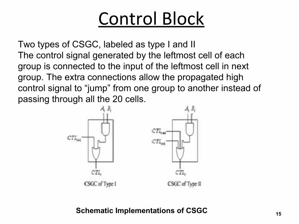
Schematic Implementations of CSGC
Two types of CSGC, labeled as type I and II The control signal generated by the leftmost cell of each group is connected to the input of the leftmost cell in next group. The extra connections allow the propagated high control signal to “jump” from one group to another instead of passing through all the 20 cells.
16
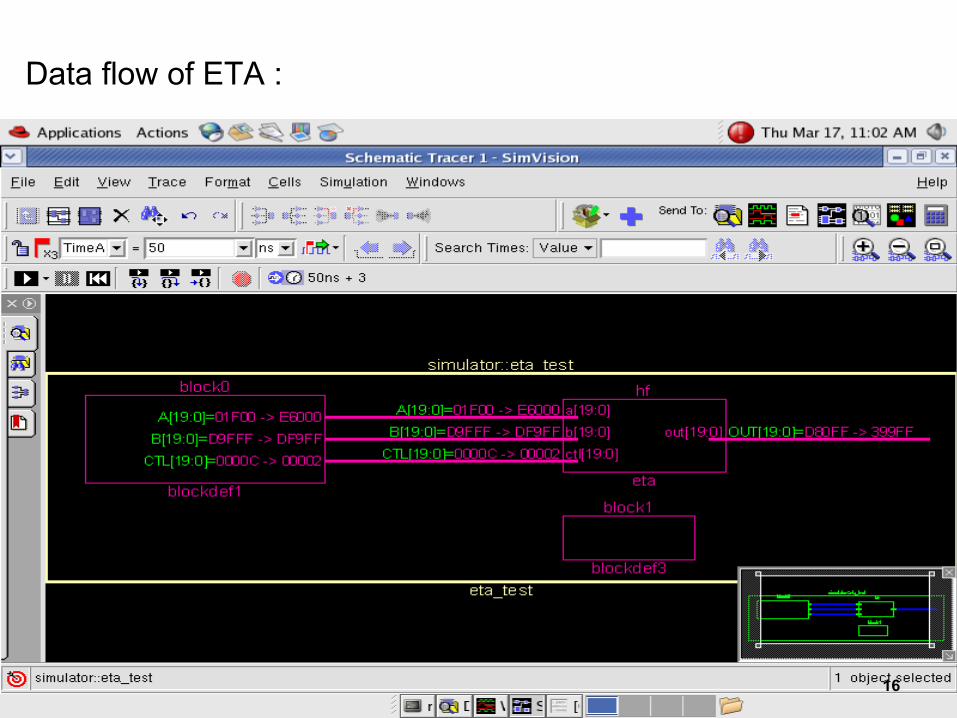
Data flow of ETA :
17
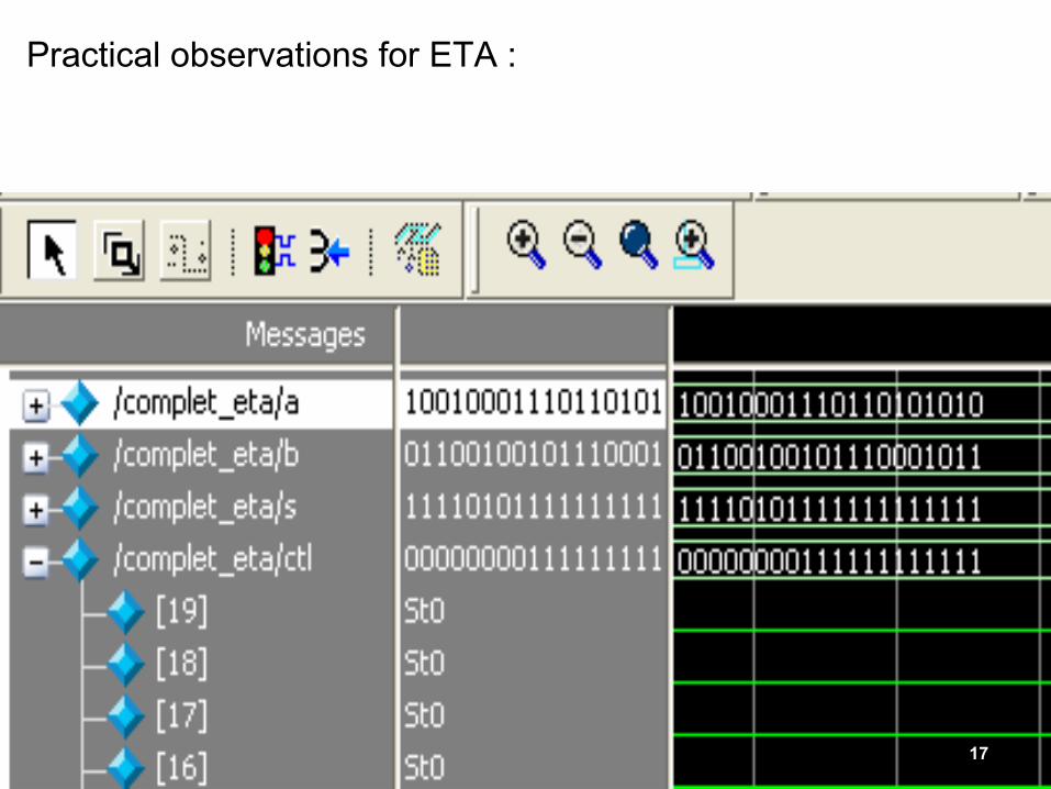
Practical observations for ETA :
With a NAND and an XOR available simultaneously in a single cell, the AT6000 architecture is ideally suited for implementing arithmetic operations, including parallel adders.
Ripple-carry adder – the simplest and most compact parallel adders – require as little as four cells per bit, and one layout has a carry delay of only one cell per bit.
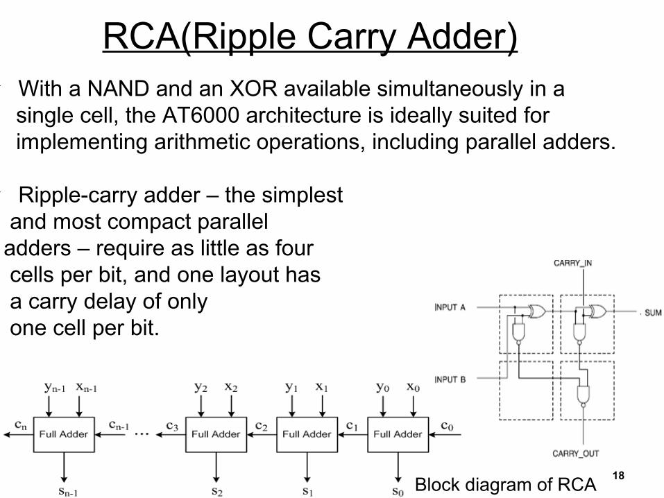
RCA(Ripple Carry Adder)
18Block diagram of RCA
19
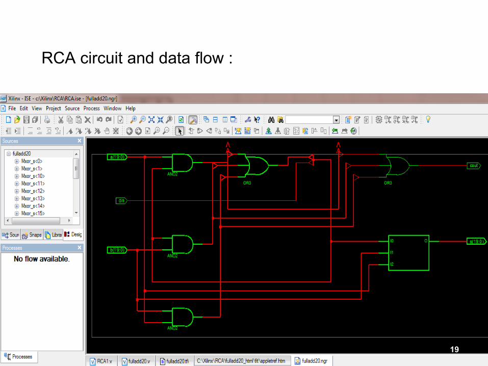
RCA circuit and data flow :
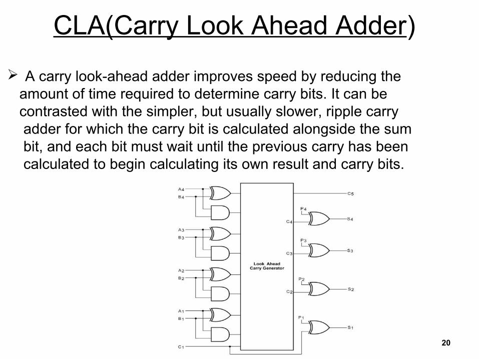
A carry look-ahead adder improves speed by reducing the amount of time required to determine carry bits. It can be contrasted with the simpler, but usually slower, ripple carry adder for which the carry bit is calculated alongside the sum bit, and each bit must wait until the previous carry has been calculated to begin calculating its own result and carry bits.
CLA(Carry Look Ahead Adder)
20
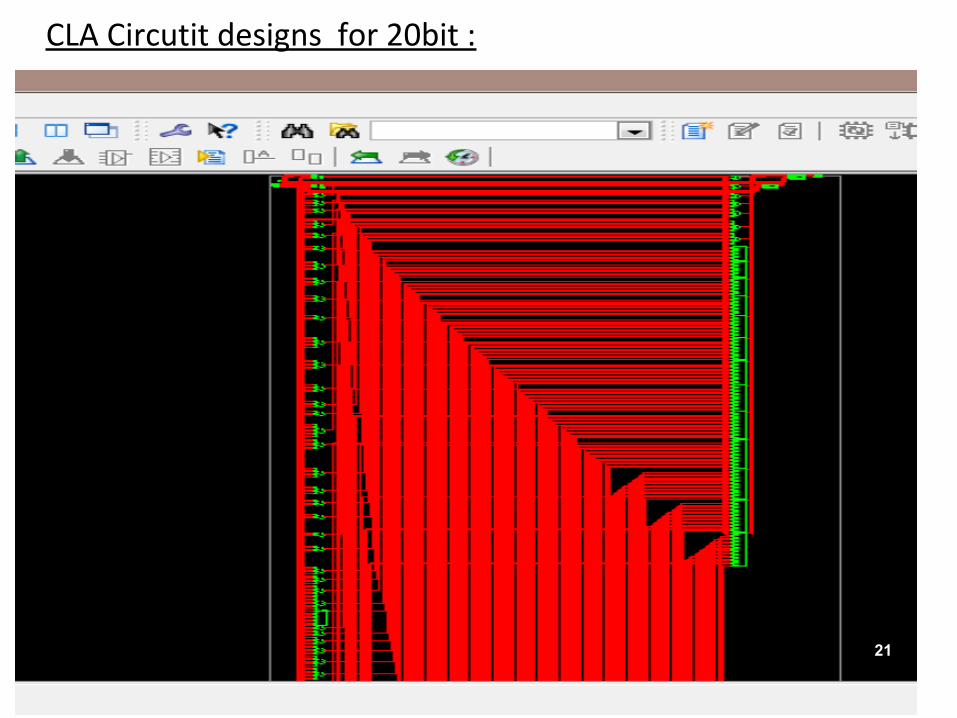
CLA Circutit designs for 20bit :
21
22
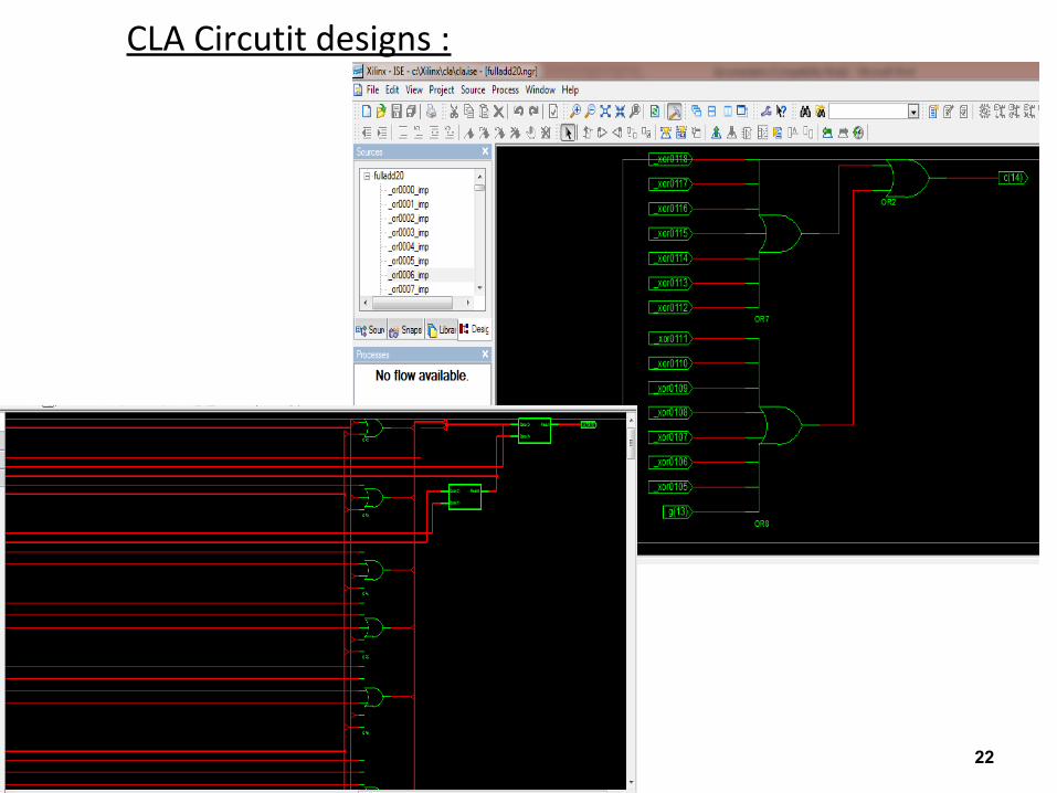
CLA Circutit designs :
23
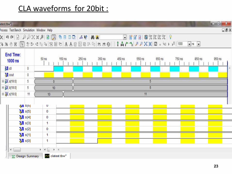
CLA waveforms for 20bit :
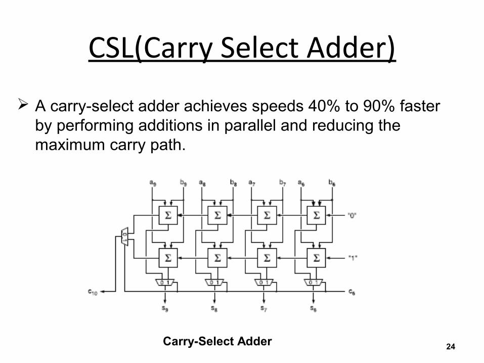
CSL(Carry Select Adder)
24Carry-Select Adder
A carry-select adder achieves speeds 40% to 90% faster by performing additions in parallel and reducing the maximum carry path.
CSL(Carry Select Adder)
25
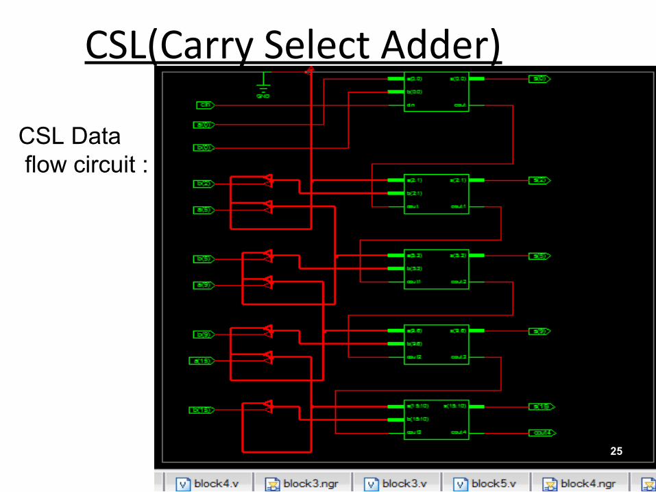
CSL Data flow circuit :
26
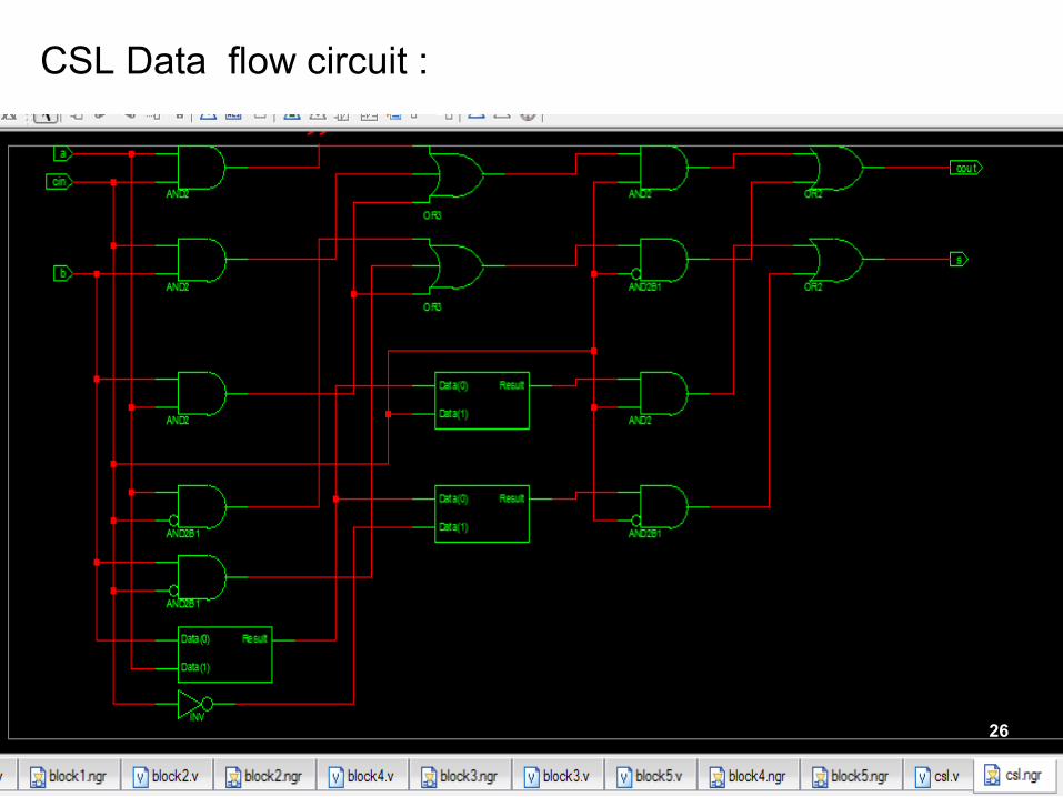
CSL Data flow circuit :
27
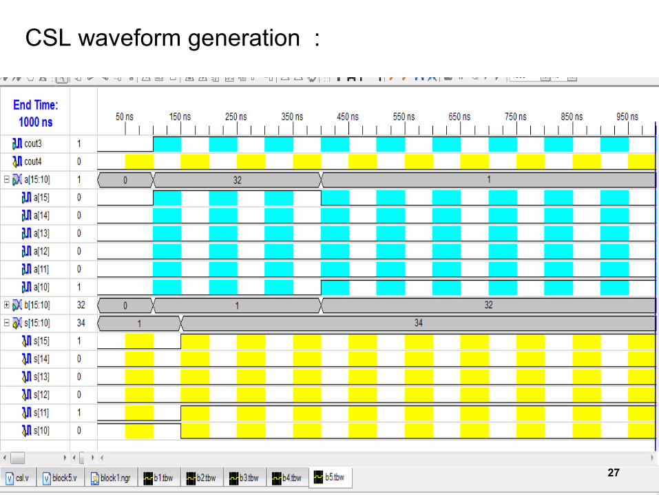
CSL waveform generation :
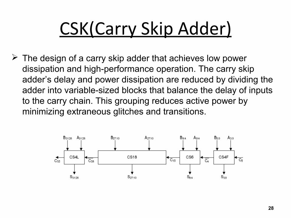
CSK(Carry Skip Adder)
28
The design of a carry skip adder that achieves low power dissipation and high-performance operation. The carry skip adder’s delay and power dissipation are reduced by dividing the adder into variable-sized blocks that balance the delay of inputs to the carry chain. This grouping reduces active power by minimizing extraneous glitches and transitions.
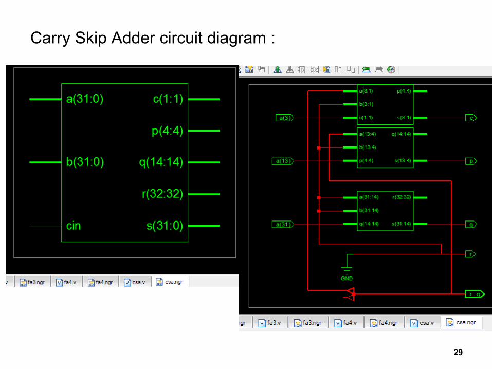
29
Carry Skip Adder circuit diagram :
30
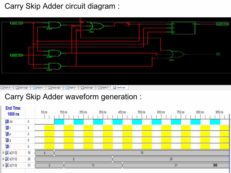
Carry Skip Adder circuit diagram :
Carry Skip Adder waveform generation :
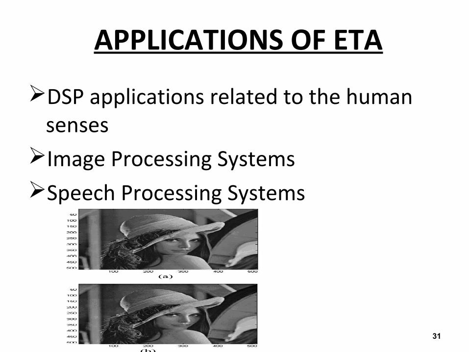
APPLICATIONS OF ETA
DSP applications related to the human senses
Image Processing SystemsSpeech Processing Systems
31
APPLICATIONS OF ETA
32
In image processing and many other DSP applications, fast Fourier transformation (FFT) is a very important function. The computational process of FFT involves a large number of additions and multiplications.
It is therefore a good platform for embedding our proposed ETA. To prove the feasibility of the ETA, we replaced all the common additions involved in a normal FFT algorithm with our proposed addition arithmetic.
CONCLUSION
33
The error-tolerant adder, which trades certain amount of accuracy for significant power saving and performance improvement, is proposed. Extensive comparisons with conventional digital adders showed that the proposed ETA outperformed the conventional adders in both power consumption and speed performance.
The potential applications of the ETA fall mainly in areas where there is no strict requirement on accuracy or where super low power consumption and high-speed performance are more important than accuracy. One example of such applications is in the DSP application for portable devices such as cell phones and laptops.

34