Embed Size (px)
Citation preview
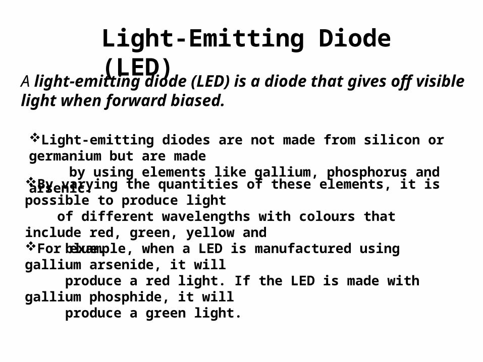
Light-Emitting Diode (LED)
A light-emitting diode (LED) is a diode that gives off visible light when forward biased.
Light-emitting diodes are not made from silicon or germanium but are made by using elements like gallium, phosphorus and arsenic.
By varying the quantities of these elements, it is possible to produce light of different wavelengths with colours that include red, green, yellow and blue.
For example, when a LED is manufactured using gallium arsenide, it will produce a red light. If the LED is made with gallium phosphide, it will produce a green light.
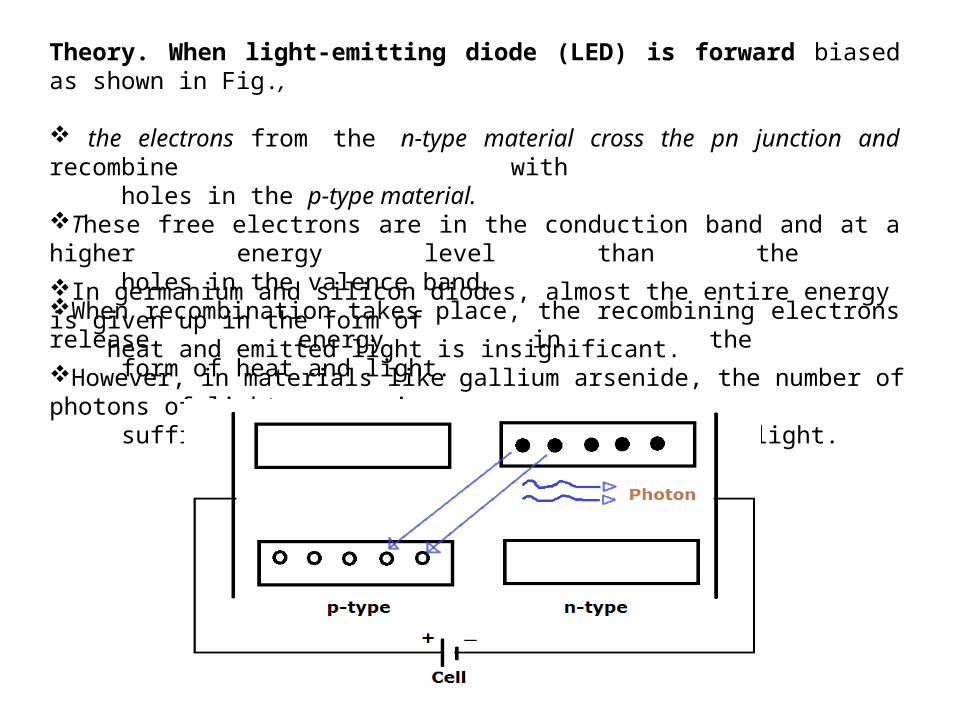
Theory. When light-emitting diode (LED) is forward biased as shown in Fig.,
the electrons from the n-type material cross the pn junction and recombine with holes in the p-type material. These free electrons are in the conduction band and at a higher energy level than the
holes in the valence band. When recombination takes place, the recombining electrons release energy in the form of heat and light.In germanium and silicon diodes, almost the entire energy is given up in the form of heat and emitted light is insignificant. However, in materials like gallium arsenide, the number of photons of light energy is sufficient to produce quite intense visible light.


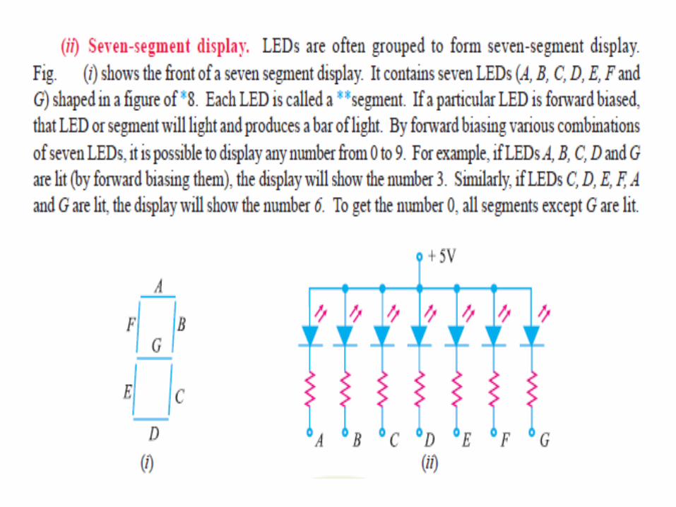

Fig. (ii) shows the schematic diagram of seven-segment display. External series resistors are included to limit currents to safe levels. Note that the anodes of all seven LEDs are connected to a common positive voltage source of +5 V. This arrangement is known as *common-anode type. In order to light a particular LED, say A, we ground the point A in Fig. 7.9 (ii). It forward biases the LED A which will be lit.

A LED that emits one colour when forward biased and another colour when reverse biased is called a multicolour LED.
One commonly used schematic symbol for these LEDs is shown in Fig.
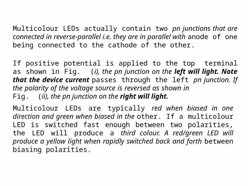
Multicolour LEDs actually contain two pn junctions that are connected in reverse-parallel i.e. they are in parallel with anode of one being connected to the cathode of the other.
If positive potential is applied to the top terminal as shown in Fig. (i), the pn junction on the left will light. Note that the device current passes through the left pn junction. If the polarity of the voltage source is reversed as shown in Fig. (ii), the pn junction on the right will light.
Multicolour LEDs are typically red when biased in one direction and green when biased in the other. If a multicolour LED is switched fast enough between two polarities, the LED will produce a third colour. A red/green LED will produce a yellow light when rapidly switched back and forth between biasing polarities.
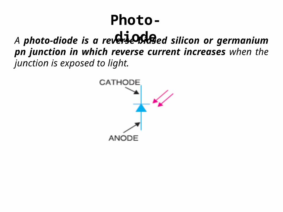
Photo-diodeA photo-diode is a reverse-biased silicon or germanium pn junction in which reverse current increases when the junction is exposed to light.

Photo-diode Operation
(ii) When light is incident on the pn junction of the photo- diode, there is a transfer of energy from the incident light (photons) to the atoms in the junction. This will create more free electrons (and more holes). These additional free electrons will increase the reverse current.(iii) As the intensity of light increases, the reverse current IR goes on increasing till it becomes maximum. This is called saturation current.
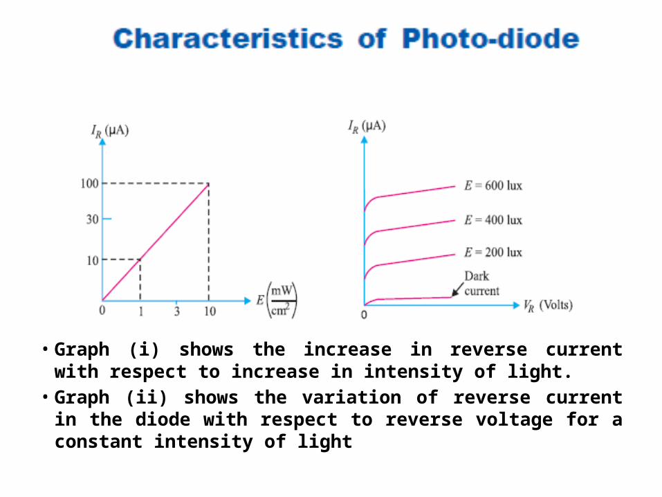
• Graph (i) shows the increase in reverse current with respect to increase in intensity of light.
• Graph (ii) shows the variation of reverse current in the diode with respect to reverse voltage for a constant intensity of light

Applications of Photo-diodes(i) Alarm circuit using photo-diode. Fig.shows the use of photo-diode in an alarm system. Light from a light source is allowed to fall on a photo-diode fitted in the doorway. The reverse current IR will continue to flow so long as the light beam is not broken. If a person passes through the door, light beam is broken and the reverse current drops to the dark current level. As a result, an alarm is sounded.
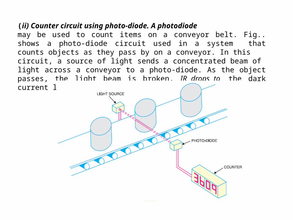
(ii) Counter circuit using photo-diode. A photodiodemay be used to count items on a conveyor belt. Fig.. shows a photo-diode circuit used in a system that counts objects as they pass by on a conveyor. In thiscircuit, a source of light sends a concentrated beam of light across a conveyor to a photo-diode. As the object passes, the light beam is broken, IR drops to the dark current level and the count is increased by one.
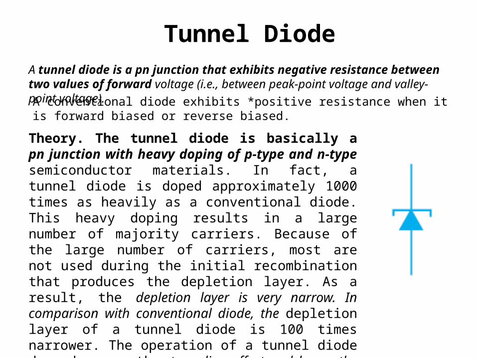
Tunnel DiodeA tunnel diode is a pn junction that exhibits negative resistance between two values of forward voltage (i.e., between peak-point voltage and valley-point voltage).A conventional diode exhibits *positive resistance when it is forward biased or reverse biased.
Theory. The tunnel diode is basically a pn junction with heavy doping of p-type and n-type semiconductor materials. In fact, a tunnel diode is doped approximately 1000 times as heavily as a conventional diode. This heavy doping results in a large number of majority carriers. Because of the large number of carriers, most are not used during the initial recombination that produces the depletion layer. As a result, the depletion layer is very narrow. In comparison with conventional diode, the depletion layer of a tunnel diode is 100 times narrower. The operation of a tunnel diode depends upon the tunneling effect and hence the name.
Tunneling effect.The movement of valence electrons from the valence energy band to the conduction band with little or no applied forward voltage is called tunneling. Valence electrons seem to tunnel through the forbidden energy band.As the forward voltage is first increased, the diode current rises rapidly due to tunneling effect. Soon the tunneling effect is reduced and current flow starts to decrease as the forward voltage across the diode is increased. The tunnel diode is said to have entered the negative resistance region. As thevoltage is further increased, the tunneling effect plays less and less part until a valley-point is reached. From now onwards, the tunnel diode behaves as ordinary diode i.e., diode current increases with the increase in forward voltage.
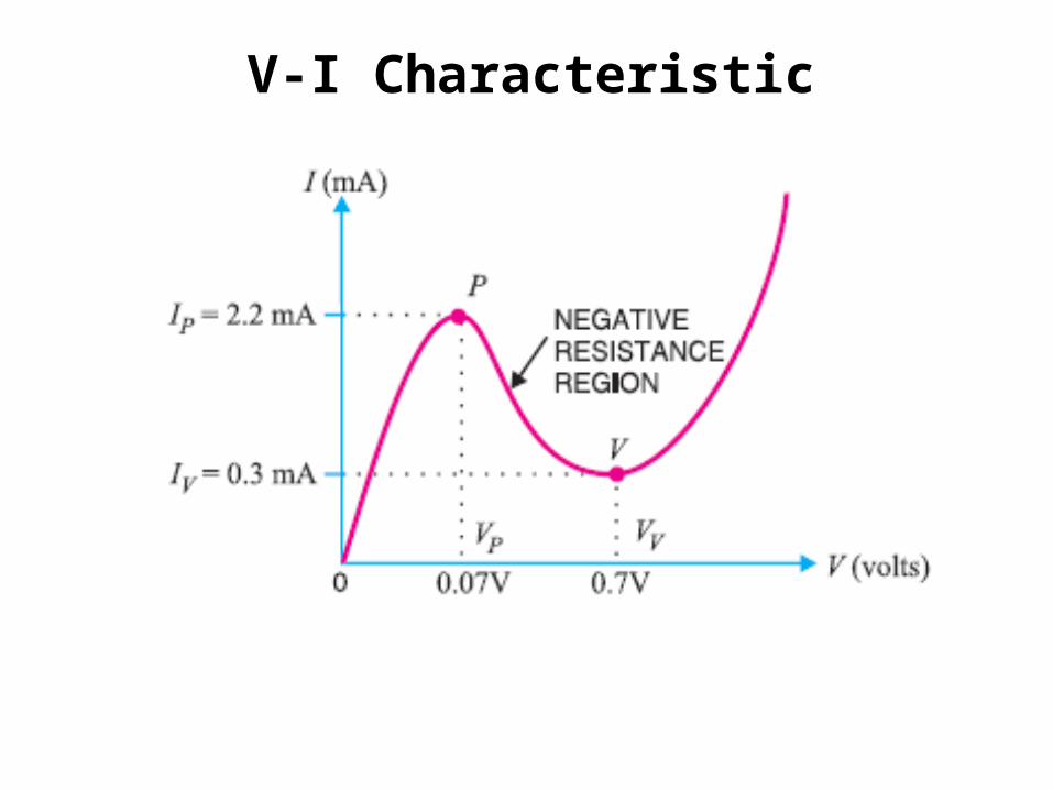
V-I Characteristic
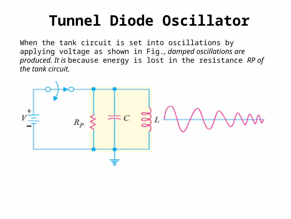
Tunnel Diode OscillatorWhen the tank circuit is set into oscillations by applying voltage as shown in Fig., damped oscillations are produced. It is because energy is lost in the resistance RP of the tank circuit.
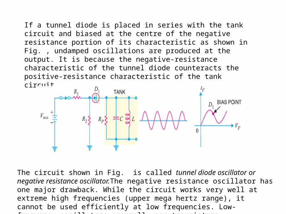
If a tunnel diode is placed in series with the tank circuit and biased at the centre of the negative resistance portion of its characteristic as shown in Fig. , undamped oscillations are produced at the output. It is because the negative-resistance characteristic of the tunnel diode counteracts the positive-resistance characteristic of the tank circuit.
The circuit shown in Fig. is called tunnel diode oscillator or negative resistance oscillator.The negative resistance oscillator has one major drawback. While the circuit works very well at extreme high frequencies (upper mega hertz range), it cannot be used efficiently at low frequencies. Low-frequency oscillators generally use transistors.
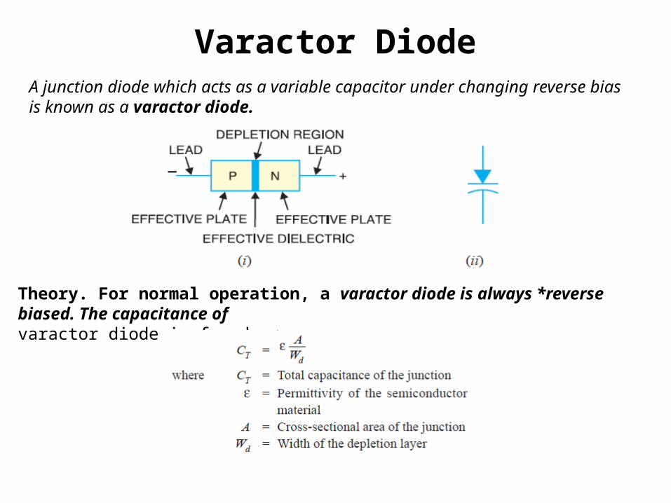
Varactor DiodeA junction diode which acts as a variable capacitor under changing reverse bias is known as a varactor diode.
Theory. For normal operation, a varactor diode is always *reverse biased. The capacitance ofvaractor diode is found as :
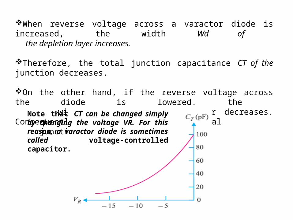
When reverse voltage across a varactor diode is increased, the width Wd of the depletion layer increases.
Therefore, the total junction capacitance CT of the junction decreases.
On the other hand, if the reverse voltage across the diode is lowered, the width Wd of the depletion layer decreases. Consequently, the total junction capacitance CT increases.
Note that CT can be changed simply by changing the voltage VR. For this reason, a varactor diode is sometimes called voltage-controlled capacitor.

Application of Varactor Diode

For normal operation, a varactor diode is always operated under reverse bias. In fact, this condition is met in the circuit shown in Fig.
The varactor diode along with the inductance connected in parallel acts as a tank circuit.
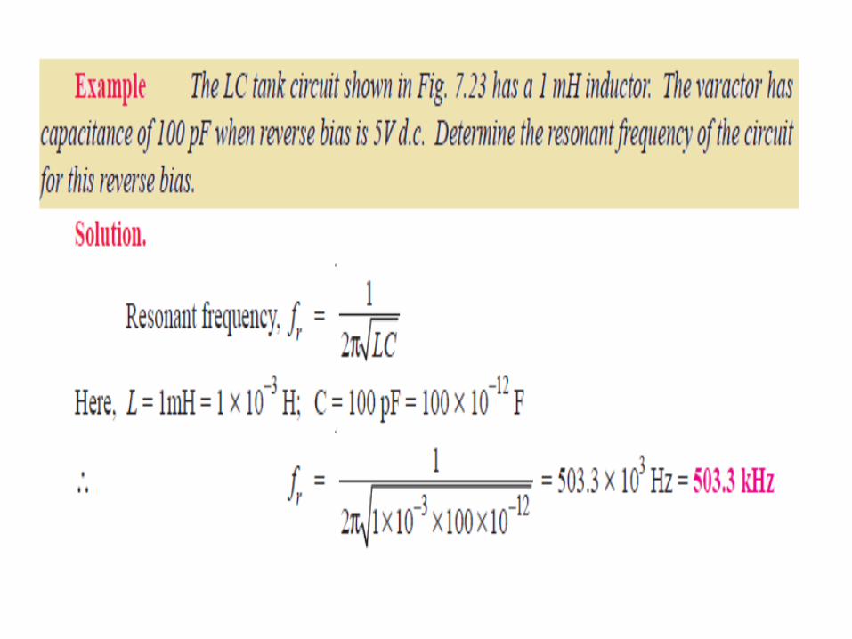
The resonant frequency fr of the LC circuit is given by;
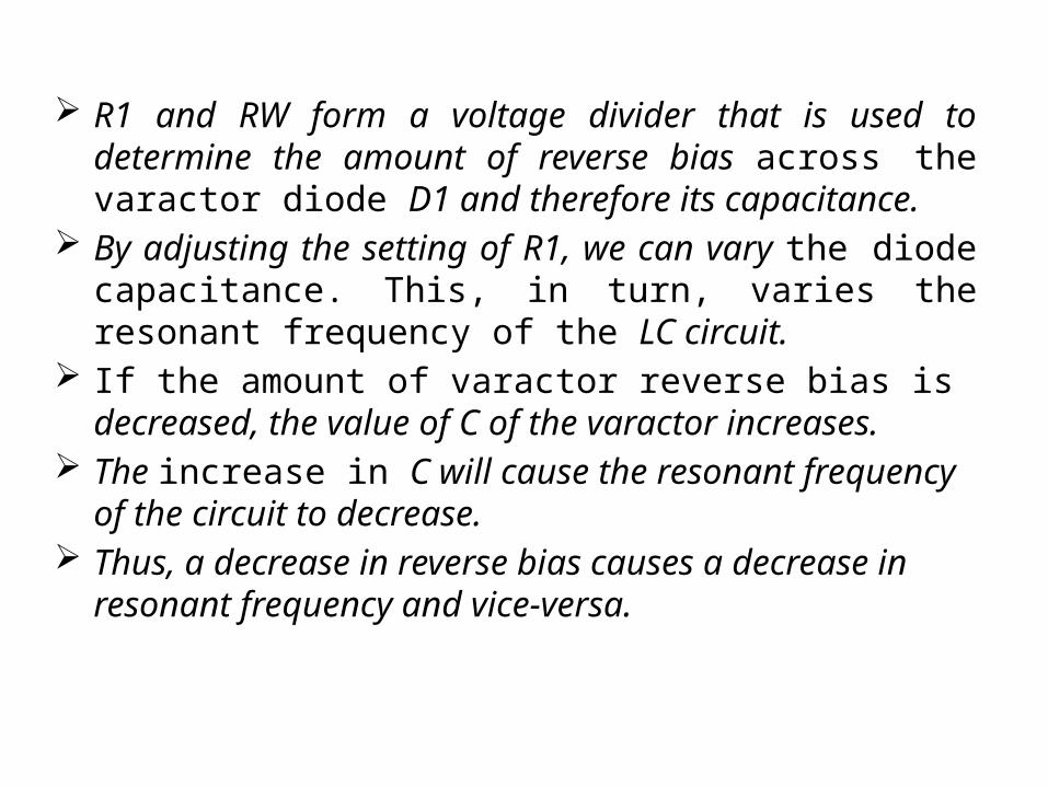
R1 and RW form a voltage divider that is used to determine the amount of reverse bias across the varactor diode D1 and therefore its capacitance.
By adjusting the setting of R1, we can vary the diode capacitance. This, in turn, varies the resonant frequency of the LC circuit.
If the amount of varactor reverse bias is decreased, the value of C of the varactor increases.
The increase in C will cause the resonant frequency of the circuit to decrease.
Thus, a decrease in reverse bias causes a decrease in resonant frequency and vice-versa.
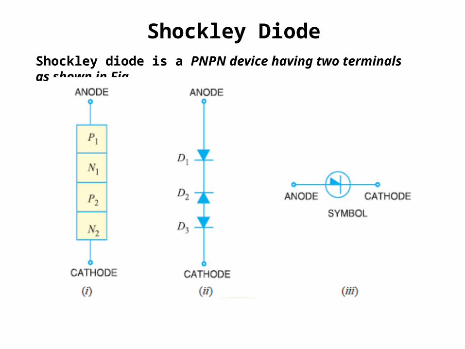
Shockley DiodeShockley diode is a PNPN device having two terminals as shown in Fig.
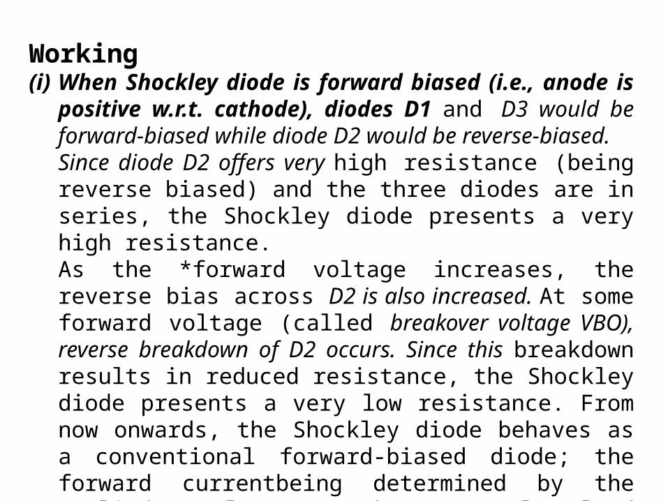
Working(i) When Shockley diode is forward biased (i.e., anode is positive
w.r.t. cathode), diodes D1 and D3 would be forward-biased while diode D2 would be reverse-biased. Since diode D2 offers very high resistance (being reverse biased) and the three diodes are in series, the Shockley diode presents a very high resistance. As the *forward voltage increases, the reverse bias across D2 is also increased. At some forward voltage (called breakover voltage VBO), reverse breakdown of D2 occurs. Since this breakdown results in reduced resistance, the Shockley diode presents a very low resistance. From now onwards, the Shockley diode behaves as a conventional forward-biased diode; the forward currentbeing determined by the applied voltage and external load resistance. This behaviour of Shockley diode is indicated on its V-I characteristic in Fig.

(ii) When Shockley diode is reverse biased (i.e., anode is negative w.r.t. cathode), diodes D1 and D3 would be reverse-biased while diode D2 would be forward-biased. If reverse voltage is increased sufficiently, the reverse voltage breakdown (point A in Fig.) of Shockley diode is reached. At this point, diodes D1 and D3 would go into reverse-voltage breakdown, the reverse current flowing through them would rise rapidly and the heat produced by this current flow could ruin the entire device. For this reason, Shockley diode should never be operated with a reverse voltage sufficient to reach the reverse-voltage breakdown point.

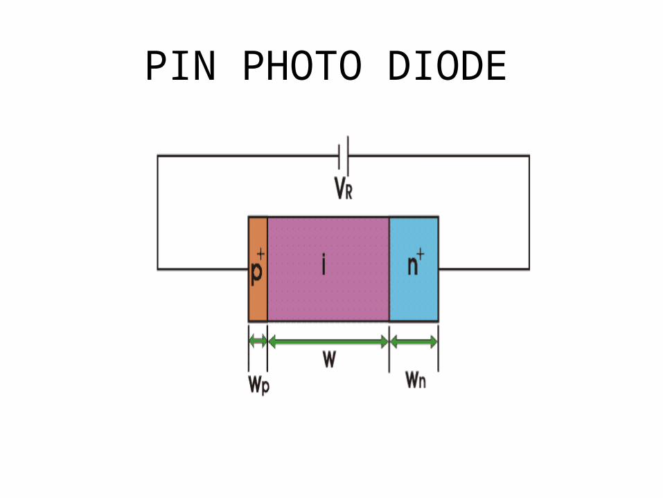
PIN PHOTO DIODE
A PIN photodiode consists of three regions- a) p- region,b) intrinsic region,c) n-region.
Light is allowed to fall on the intrinsic region. Firstly electron- hole pairs are generated by photon absorption in the intrinsic region (depletion region). These generate more electron hole pairs through impact ionization. These are swept out of the depletion region quickly, i.e, the transit time is very less. Avalanche of electrons are produced. Thus it converts light in electrical energy.

Applications of PIN diode3.1 RF and Microwave Switches3.2 RF and Microwave Variable Attenuators3.3 Limiters3.4 Photodetector and photovoltaic cell