Embed Size (px)
Citation preview
2
The basic function of transistor is to do amplification.
The weak signal is given to the base of the transistor and amplified output is obtained in the collector circuit. One important requirement during amplification is that only the magnitude of the signal should increase and there should be no change in signal shape. This increase in magnitude of the signal without any change in shape is known as faithful amplification. In order to achieve this, means are provided to ensure that input circuit (i.e. base-emitter junction) of the transistor remains forward biased and output circuit (i.e. collector base junction) always remains reverse biased during all parts of the signal. This is known as transistor biasing.
3
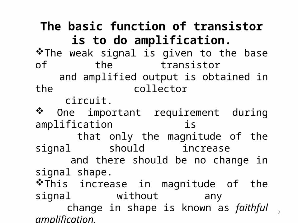
Faithful AmplificationKey factors for achieving faithful amplification:
(i) Proper zero signal collector current(ii) Minimum proper base-emitter voltage (VBE) at any instant(iii) Minimum proper collector-emitter voltage (VCE) at any instant
The conditions (i) and (ii) ensure that base- emitter junction shall remain properly forward biased during all parts of the signal. On the other hand, condition (iii) ensures that base-collector junction shall remain properly reverse biased at all times.
4
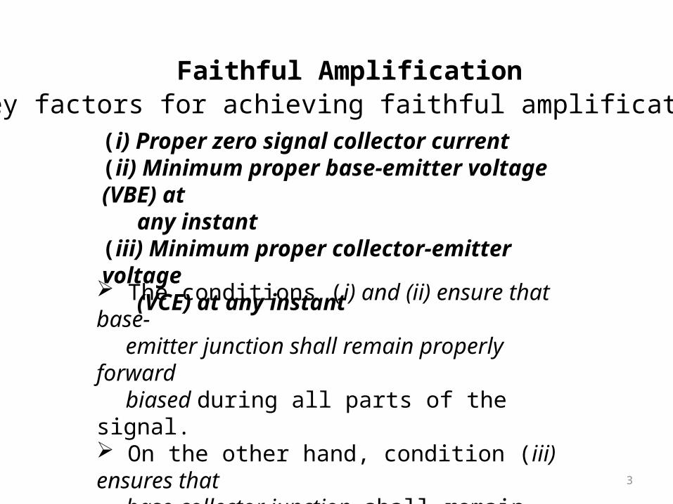
unfaithful amplification
Consider an npn transistor circuit shown in Figure.During the positive half-cycle of the signal, base is positive w.r.t. emitter and hence base emitter junction is forward biased. This will cause a base current and much larger collector current to flow in the circuit. The result is that positive half-cycle of the signal is amplified in the collector as shown.During the negative half-cycle of the signal, base-emitter junction is reverse biased and hence no current flows in the circuit. The result is that there is no output due to the negative half cycle of the signal. Thus we shall get an amplified output of the signal with its negative half-cycles completely cut off
5
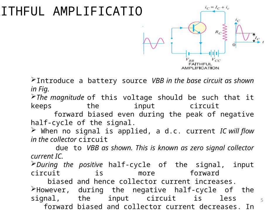
Introduce a battery source VBB in the base circuit as shown in Fig. The magnitude of this voltage should be such that it keeps the input circuit forward biased even during the peak of negative half-cycle of the signal. When no signal is applied, a d.c. current IC will flow in the collector circuit due to VBB as shown. This is known as zero signal collector current IC. During the positive half-cycle of the signal, input circuit is more forward biased and hence collector current increases. However, during the negative half-cycle of the signal, the input circuit is less forward biased and collector current decreases. In this way, negative half- cycle of the signal also appears in the output and hence faithful amplification results. It follows, therefore, that for faithful amplification, proper zero signal collector current must flow. The value of zero signal collector current should be atleast equal to the maximum collector current due to signal alone i.e. Zero signal collector current ≥ Max. collector current due to signal alone
FAITHFUL AMPLIFICATION
6
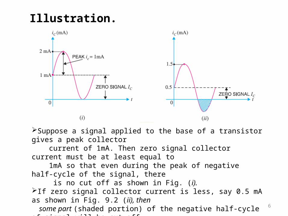
Illustration.
Suppose a signal applied to the base of a transistor gives a peak collector current of 1mA. Then zero signal collector current must be at least equal to 1mA so that even during the peak of negative half-cycle of the signal, there is no cut off as shown in Fig. (i).If zero signal collector current is less, say 0.5 mA as shown in Fig. 9.2 (ii), then
some part (shaded portion) of the negative half-cycle of signal will be cut off In the output.
7
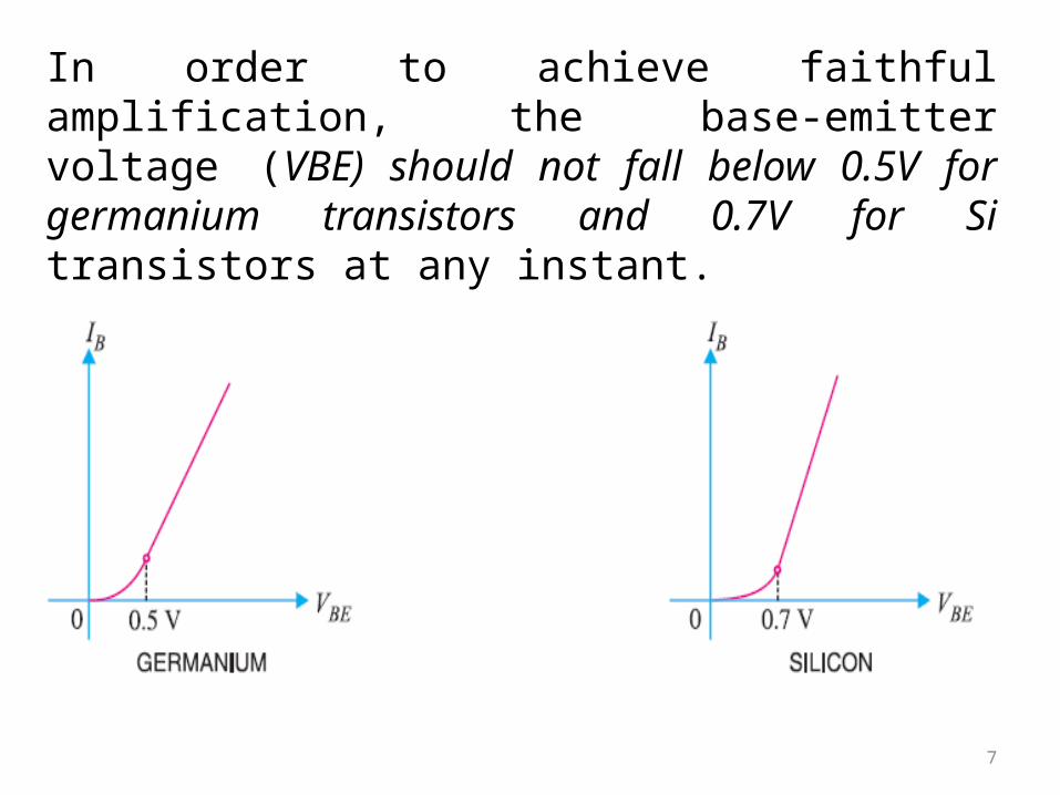
In order to achieve faithful amplification, the base-emitter voltage (VBE) should not fall below 0.5V for germanium transistors and 0.7V for Si transistors at any instant.
8
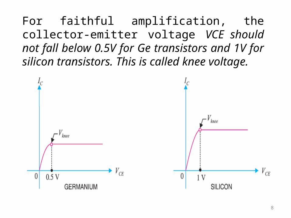
For faithful amplification, the collector-emitter voltage VCE should not fall below 0.5V for Ge transistors and 1V for silicon transistors. This is called knee voltage.
9
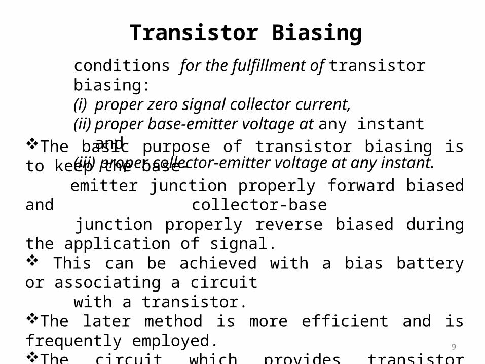
Transistor Biasingconditions for the fulfillment of transistor biasing:(i) proper zero signal collector current, (ii) proper base-emitter voltage at any instant and (iii) proper collector-emitter voltage at any instant.
The basic purpose of transistor biasing is to keep the base- emitter junction properly forward biased and collector-base junction properly reverse biased during the application of signal. This can be achieved with a bias battery or associating a circuit with a transistor. The later method is more efficient and is frequently employed. The circuit which provides transistor biasing is known as biasing circuit. It may be noted that transistor biasing is very essential for the proper operation of transistor in any circuit.
10
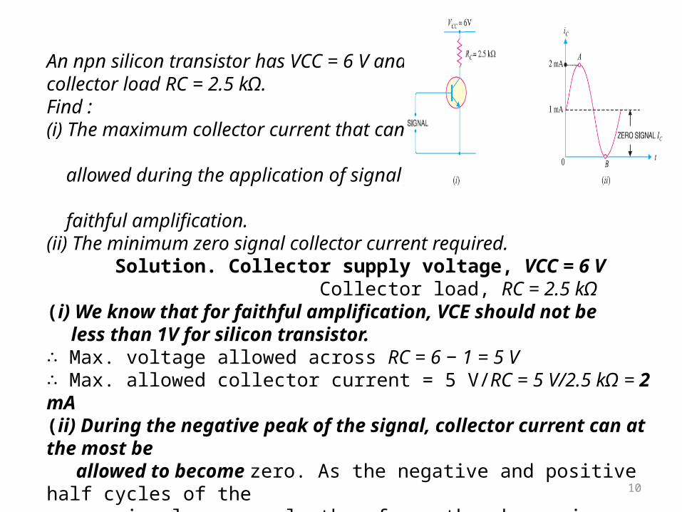
An npn silicon transistor has VCC = 6 V and the collector load RC = 2.5 kΩ.Find :(i) The maximum collector current that can be allowed during the application of signal for, faithful amplification.(ii) The minimum zero signal collector current required. Solution. Collector supply voltage, VCC = 6 V Collector load, RC = 2.5 kΩ(i) We know that for faithful amplification, VCE should not be less than 1V for silicon transistor.
∴ Max. voltage allowed across RC = 6 − 1 = 5 V ∴ Max. allowed collector current = 5 V/RC = 5 V/2.5 kΩ = 2 mA
(ii) During the negative peak of the signal, collector current can at the most be allowed to become zero. As the negative and positive half cycles of the signal are equal, therefore, the change in collector current due to these will also be equal but in opposite direction.
∴ Minimum zero signal collector current required = 2 mA/2 = 1 mA
11
12
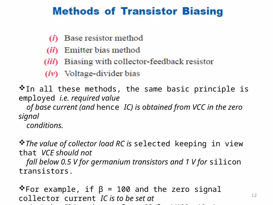
In all these methods, the same basic principle is employed i.e. required value
of base current (and hence IC) is obtained from VCC in the zero signal conditions.
The value of collector load RC is selected keeping in view that VCE should not fall below 0.5 V for germanium transistors and 1 V for silicon transistors. For example, if β = 100 and the zero signal collector current IC is to be set at 1mA, then IB is made equal to IC /β = 1/100 = 10 μA.
Thus, the biasing network should be so designed that a base current of 10 μA
flows in the zero signal conditions.
13
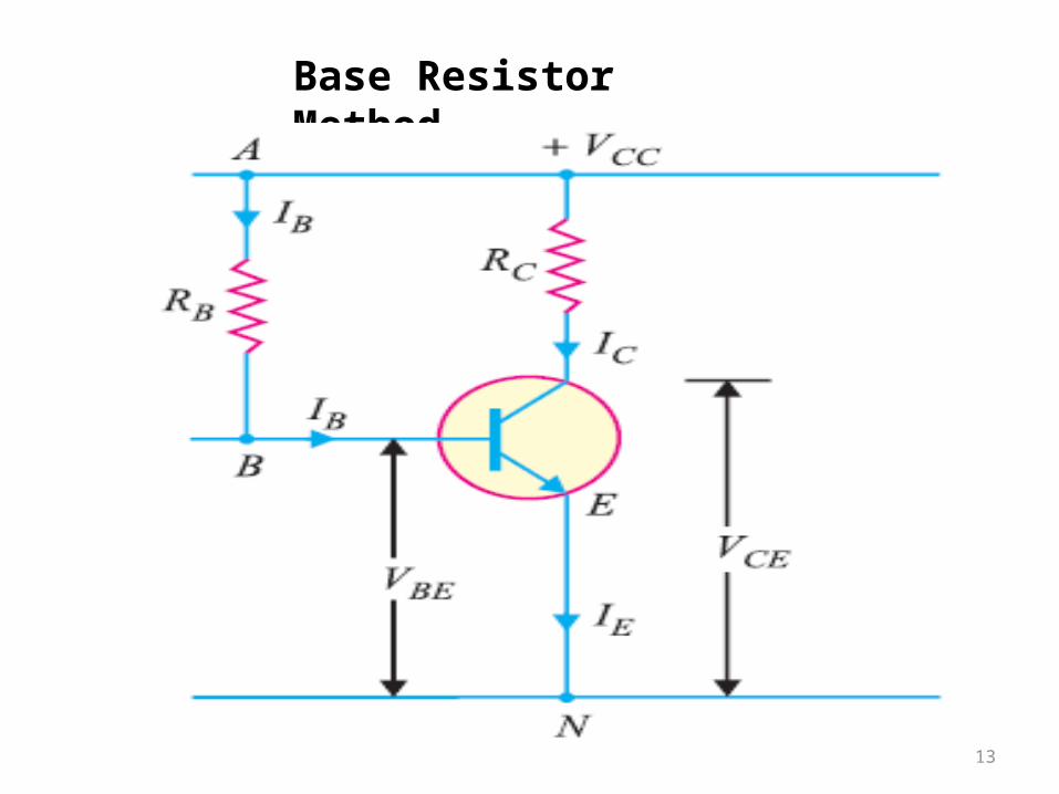
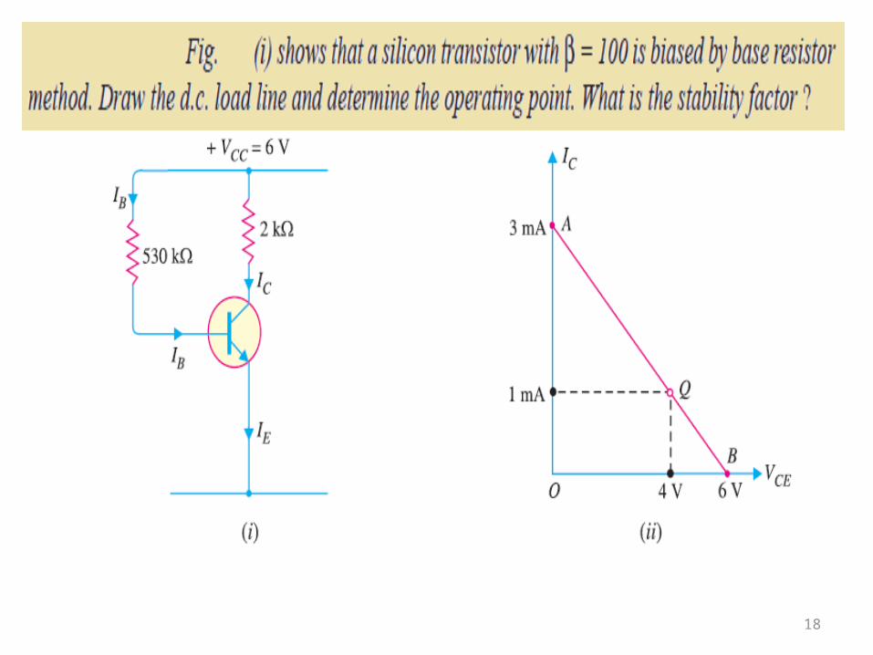
Base Resistor Method
14
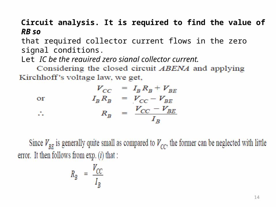
Circuit analysis. It is required to find the value of RB sothat required collector current flows in the zero signal conditions.Let IC be the required zero signal collector current.
∴ IB = IC/β
15
16
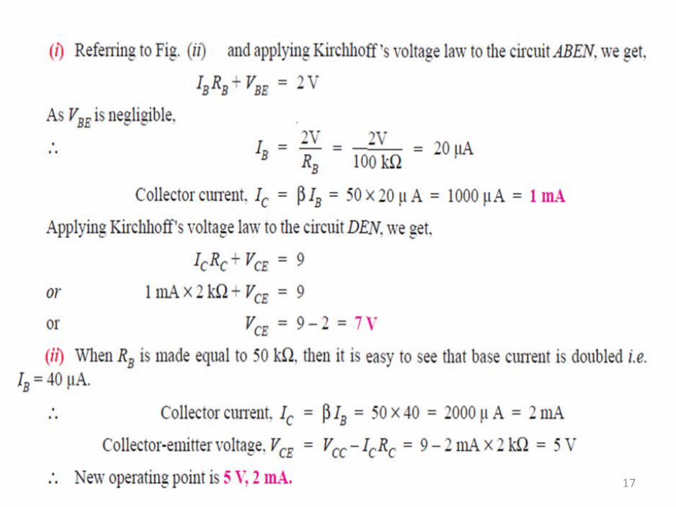
17
18
19
20
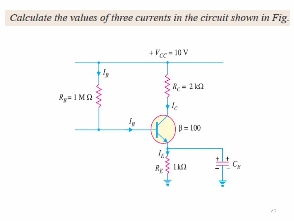
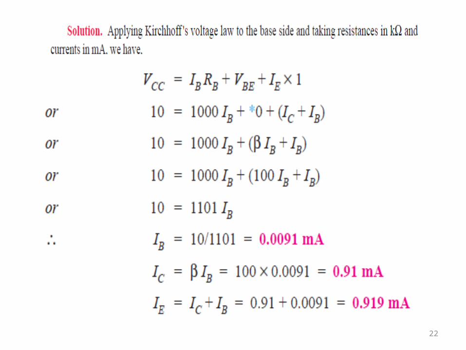
21
22
23
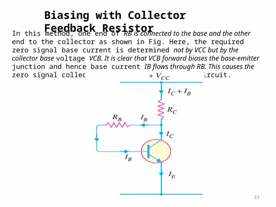
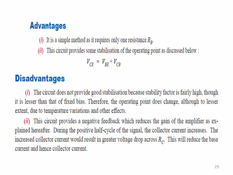
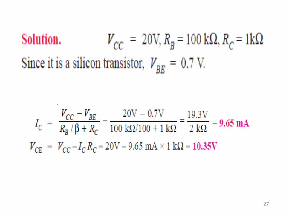
Biasing with Collector Feedback Resistor
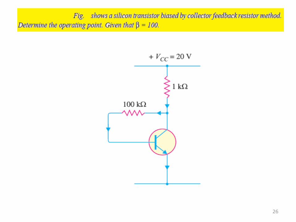
In this method, one end of RB is connected to the base and the other end to the collector as shown in Fig. Here, the required zero signal base current is determined not by VCC but by the collector base voltage VCB. It is clear that VCB forward biases the base-emitterjunction and hence base current IB flows through RB. This causes the zero signal collector current to flow in the circuit.
24
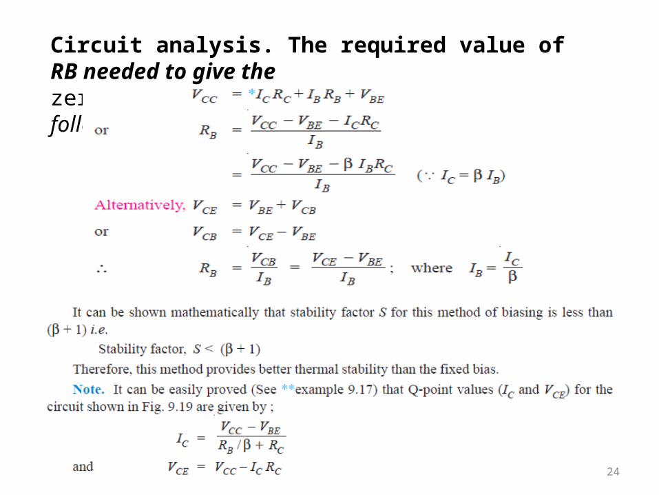
Circuit analysis. The required value of RB needed to give thezero signal current IC can be determined as follows.
25
26
27
28
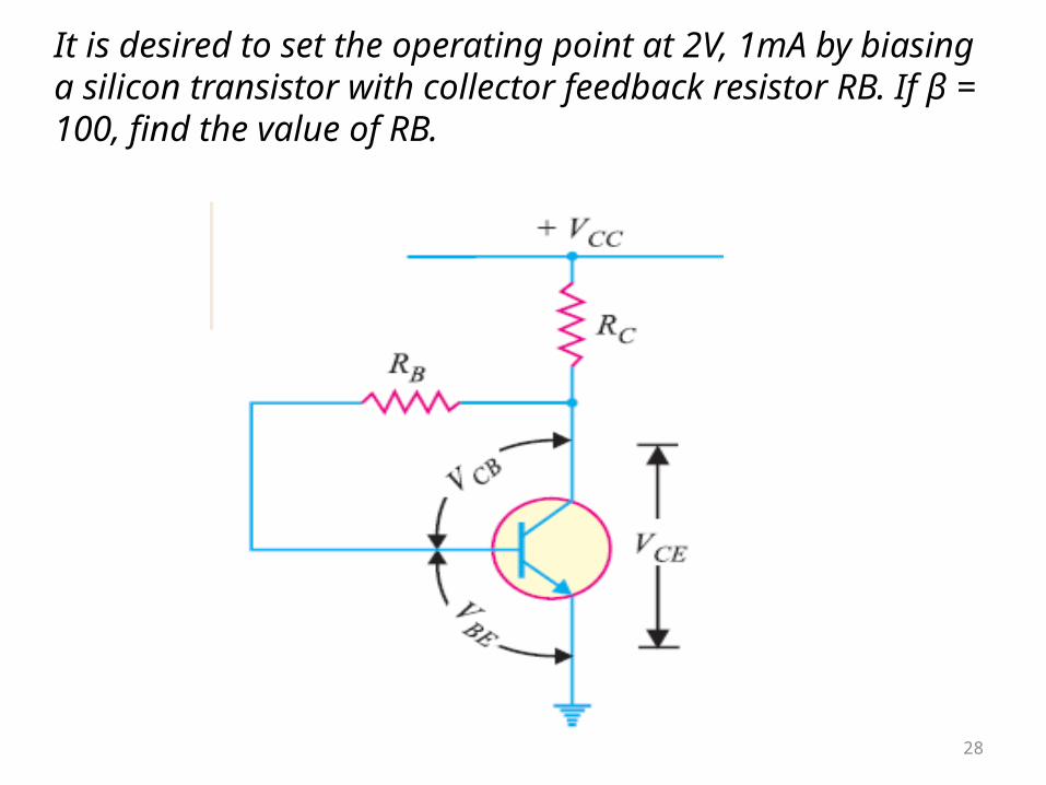
It is desired to set the operating point at 2V, 1mA by biasing a silicon transistor with collector feedback resistor RB. If β = 100, find the value of RB.
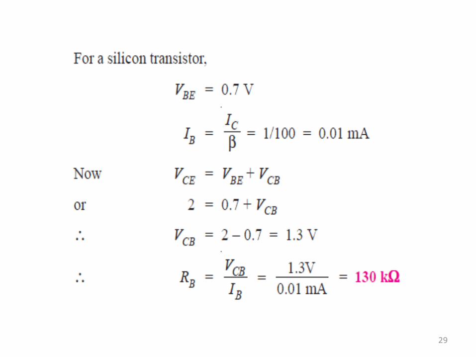
29
30
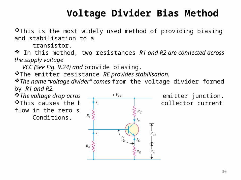
Voltage Divider Bias Method
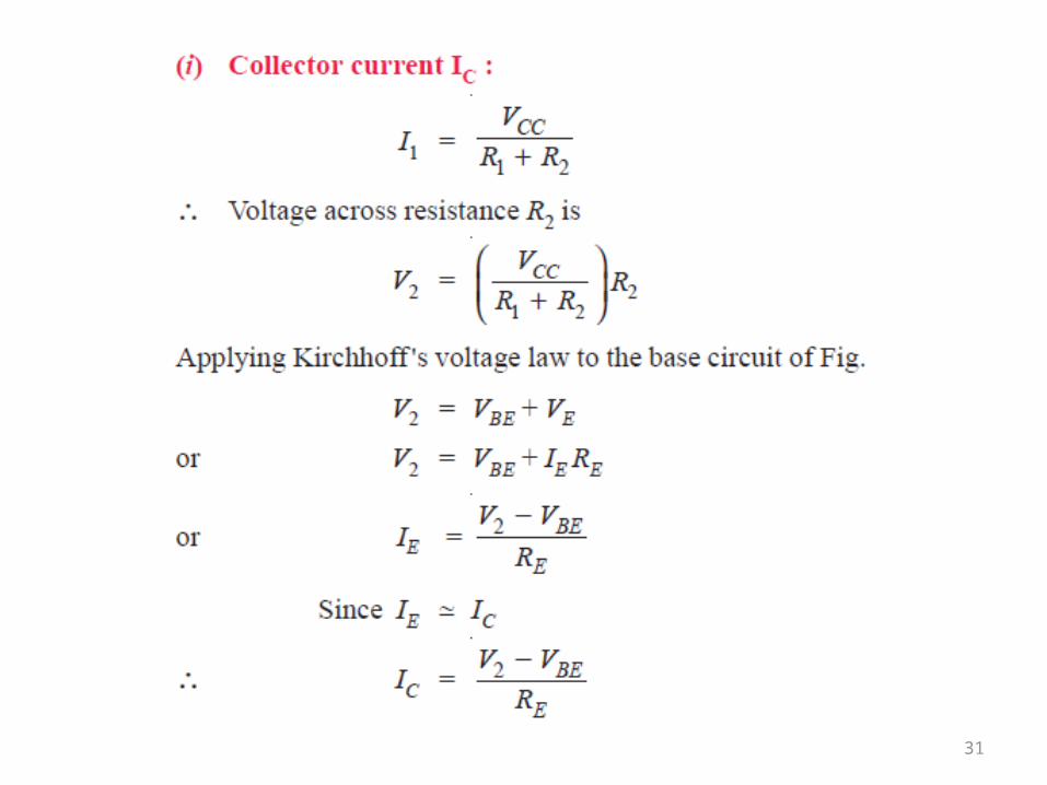
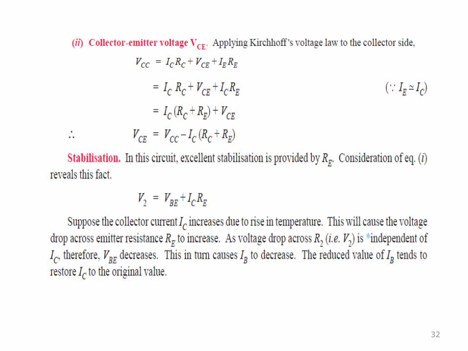
This is the most widely used method of providing biasing and stabilisation to a transistor. In this method, two resistances R1 and R2 are connected across the supply voltage VCC (See Fig. 9.24) and provide biasing. The emitter resistance RE provides stabilisation. The name ‘‘voltage divider’’ comes from the voltage divider formed by R1 and R2. The voltage drop across R2 forward biases the base- emitter junction. This causes the base current and hence collector current flow in the zero signal Conditions.
31
32
33
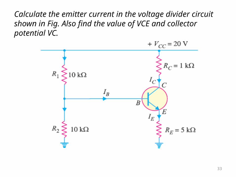
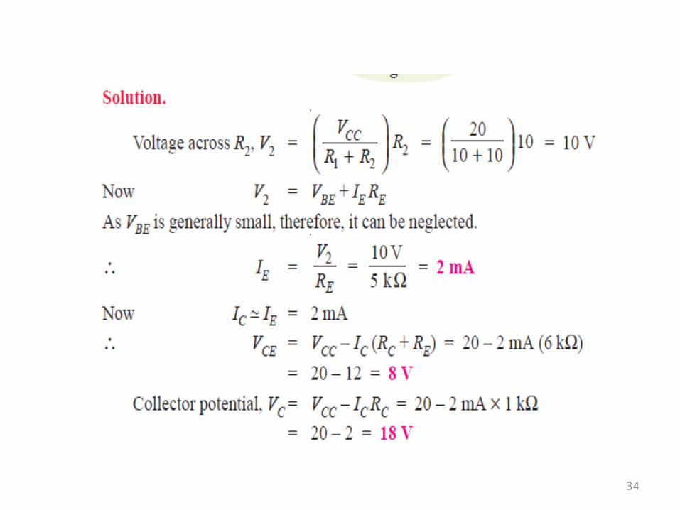
Calculate the emitter current in the voltage divider circuit shown in Fig. Also find the value of VCE and collector potential VC.
34
35
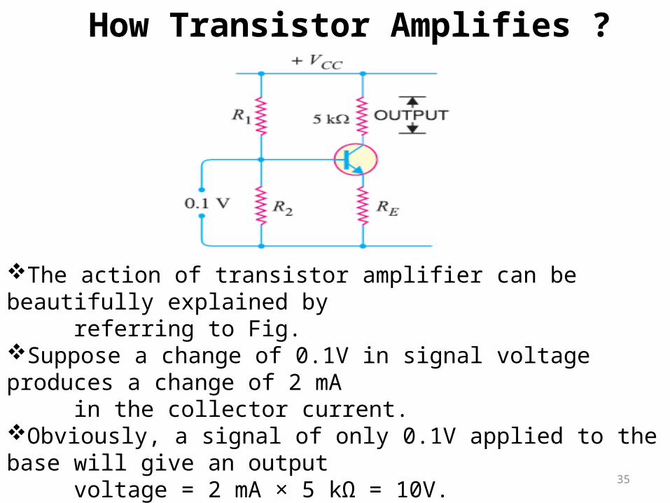
How Transistor Amplifies ?
The action of transistor amplifier can be beautifully explained by referring to Fig. Suppose a change of 0.1V in signal voltage produces a change of 2 mA
in the collector current. Obviously, a signal of only 0.1V applied to the base will give an output voltage = 2 mA × 5 kΩ = 10V. Thus, the transistor has been able to raise the voltage level of the signal from 0.1V to 10V i.e. voltage amplification or stage gain is 100.
36
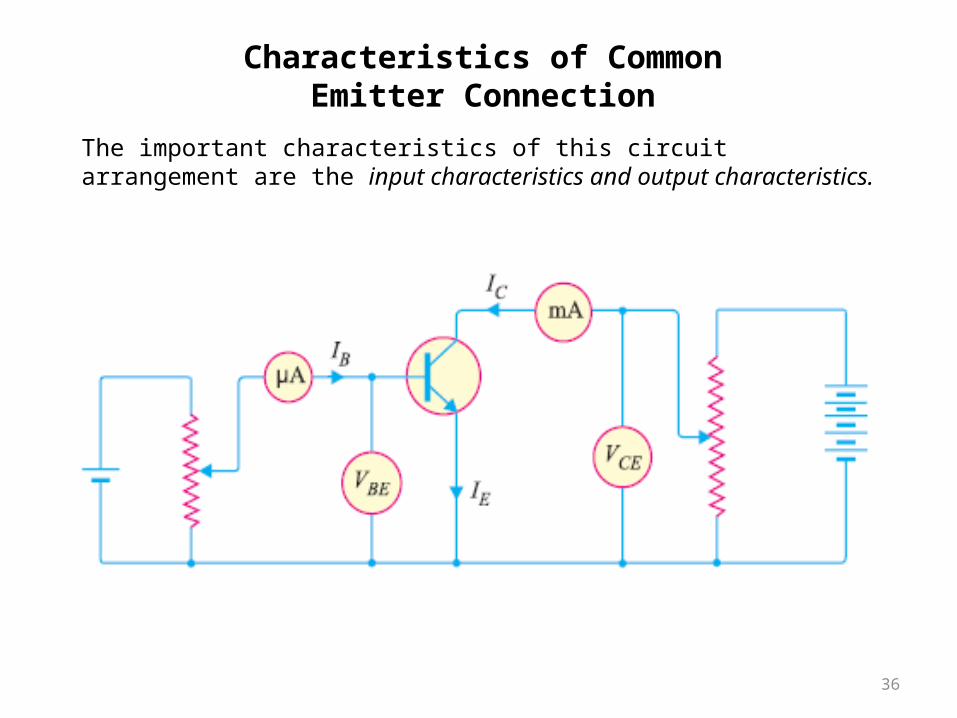
Characteristics of Common Emitter Connection
The important characteristics of this circuit arrangement are the input characteristics and output characteristics.
37
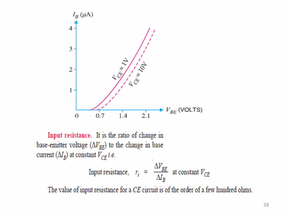
1. Input characteristic. It is the curve between base current IB and base-emitter voltage VBE at constant collector-emitter voltage VCE.The following points may be noted from the characteristics :(i) The characteristic resembles that of a forward biased diode curve. This is expected since the base-emitter section of transistor is a diode and it is forward biased.(ii) As compared to CB arrangement, IB increases less rapidly with VBE. Therefore, input resistance of a CE circuit is higher than that of CBcircuit.
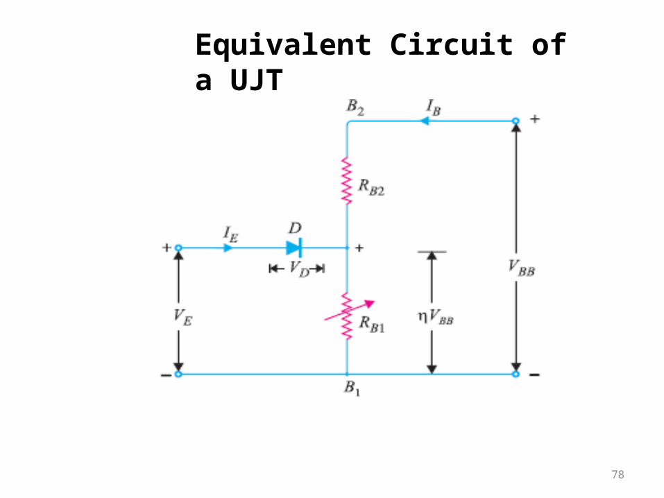
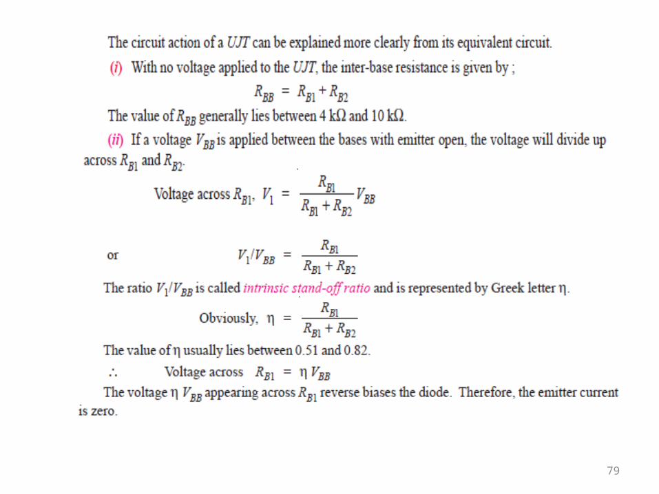
38
39
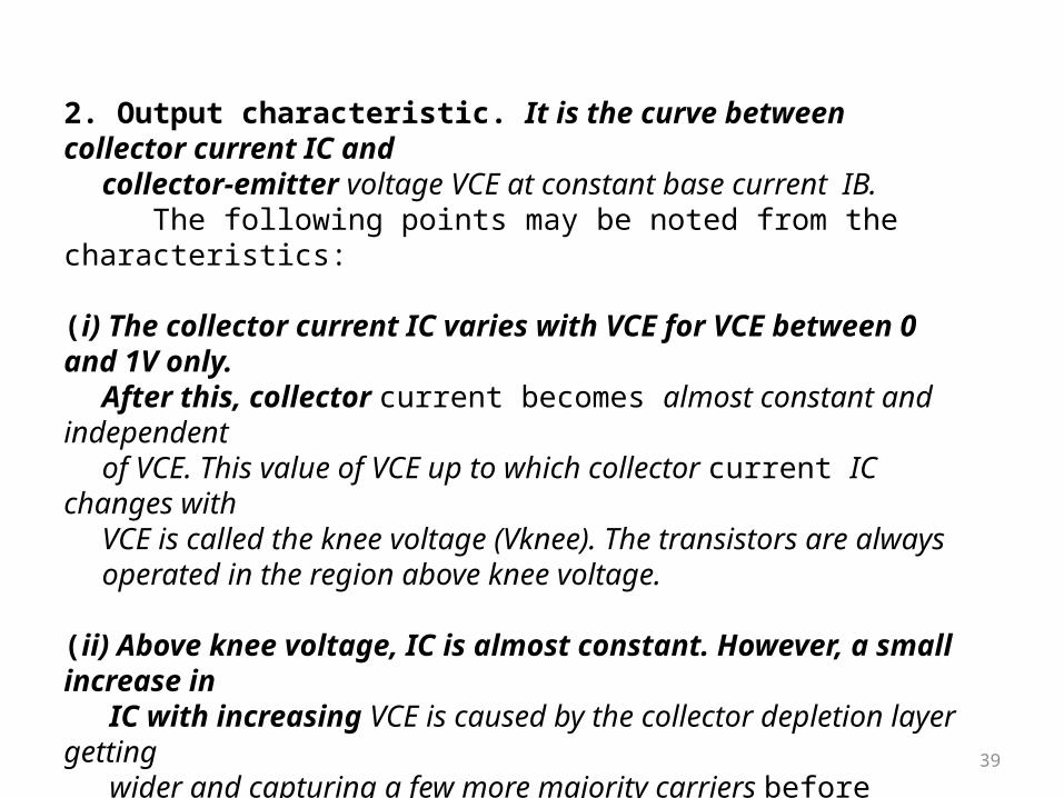
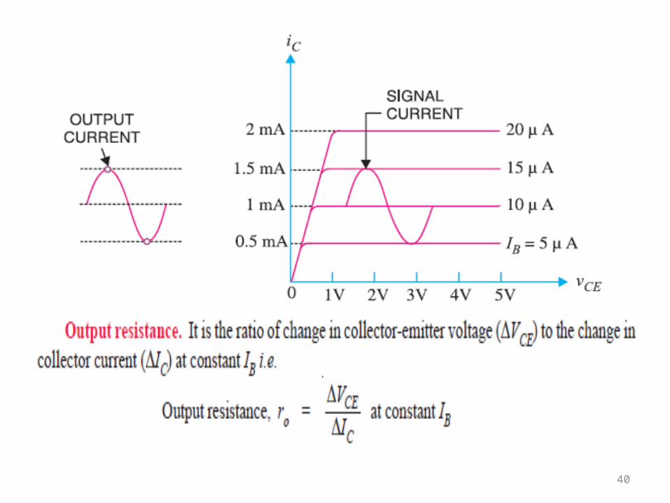
2. Output characteristic. It is the curve between collector current IC and collector-emitter voltage VCE at constant base current IB. The following points may be noted from the characteristics:
(i) The collector current IC varies with VCE for VCE between 0 and 1V only. After this, collector current becomes almost constant and independent of VCE. This value of VCE up to which collector current IC changes with VCE is called the knee voltage (Vknee). The transistors are always operated in the region above knee voltage.
(ii) Above knee voltage, IC is almost constant. However, a small increase in IC with increasing VCE is caused by the collector depletion layer getting wider and capturing a few more majority carriers before electron-hole combinations occur in the base area.
(iii) For any value of VCE above knee voltage, the collector current IC is approximately equal to β × IB.
40
41
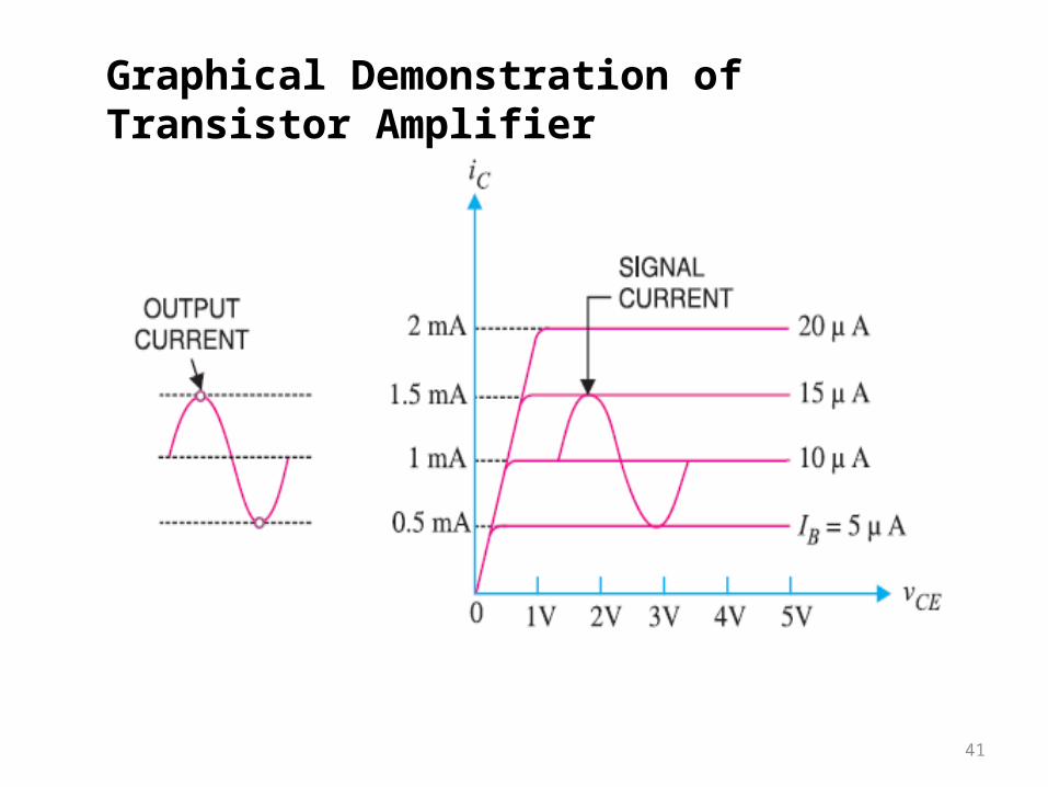
Graphical Demonstration of Transistor Amplifier
42
For example, consider a sinusoidal signal which increases or decreases the base current by 5 μA in the two half-cycles of the signal. Referring to Fig., it is clear that in the absence of signal, the base current is 10μA and the collector current is 1 mA. However, when the signal is applied in the base circuit, the base current and hence collector current change continuously. In the first half-cycle peak of the signal, the base current increases to 15 μA and the corresponding collector current is 1.5 mA. In the second half-cycle peak, the base current is reduced to 5 μA and the corresponding collector current is 0.5 mA. For other values of the signal, the collector current is in between these values i.e. 1.5 mA and 0.5 mA.It is clear from Fig. that 10 μA base current variation results in 1mA (1,000 μA) collector current variation i.e. by a factor of 100. This large change in collector current flows through collector resistance RC. The result is that output signal is much larger than the input signal. Thus, the transistor has done amplification.
43
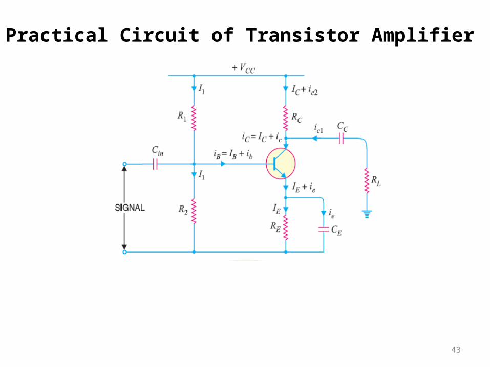
Practical Circuit of Transistor Amplifier
44
45
46
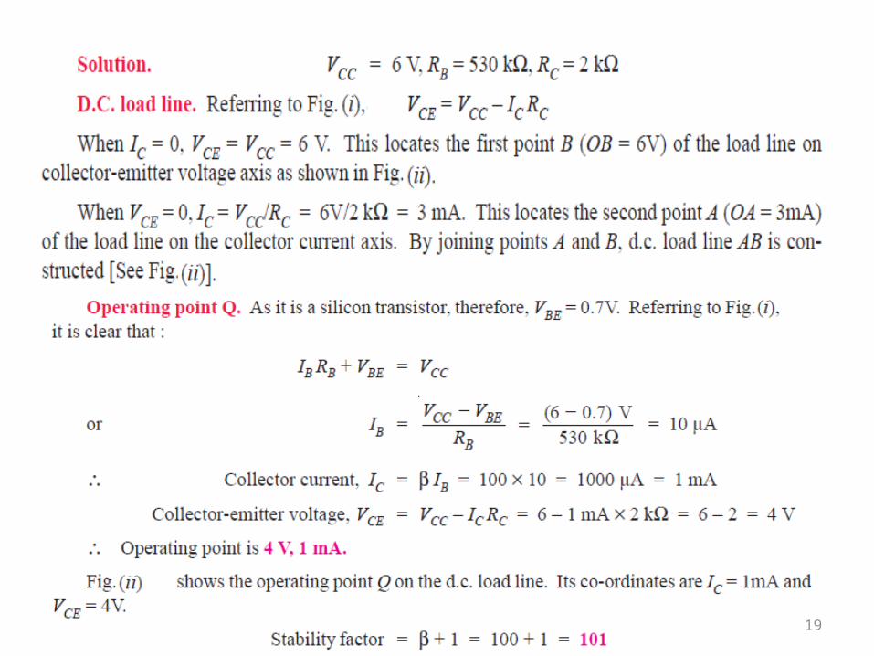
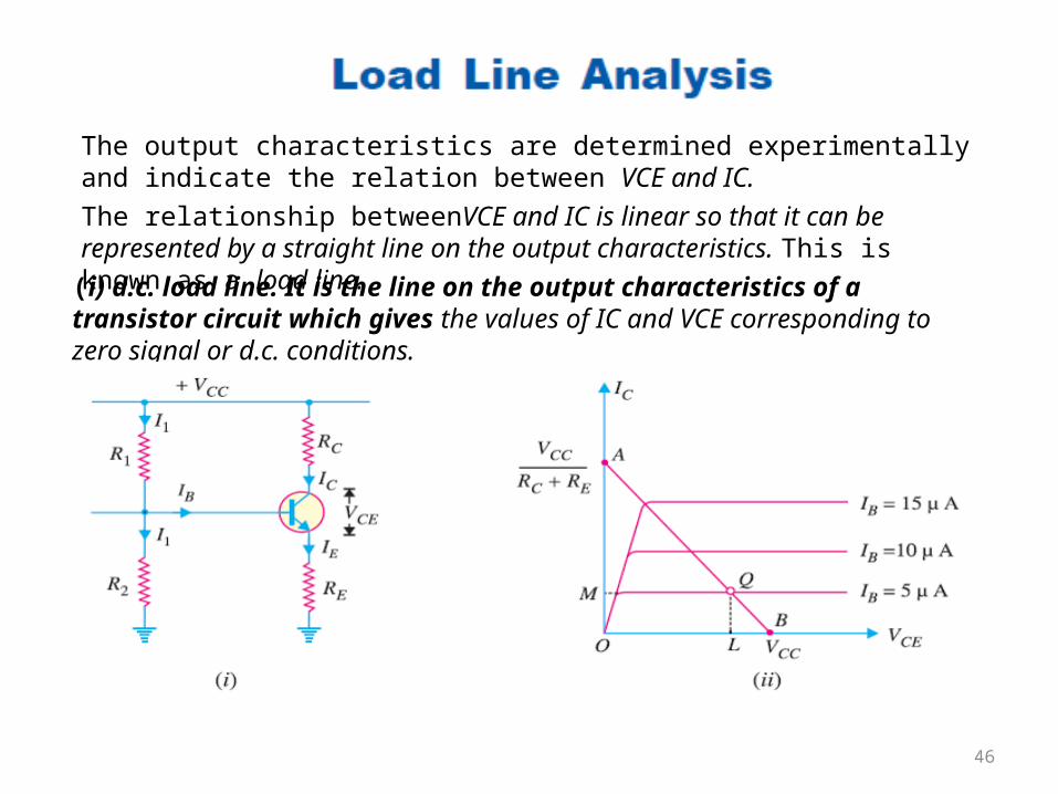
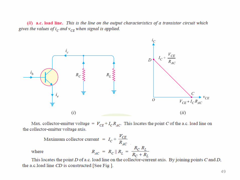
The output characteristics are determined experimentally and indicate the relation between VCE and IC.The relationship betweenVCE and IC is linear so that it can be represented by a straight line on the output characteristics. This is known as a load line.
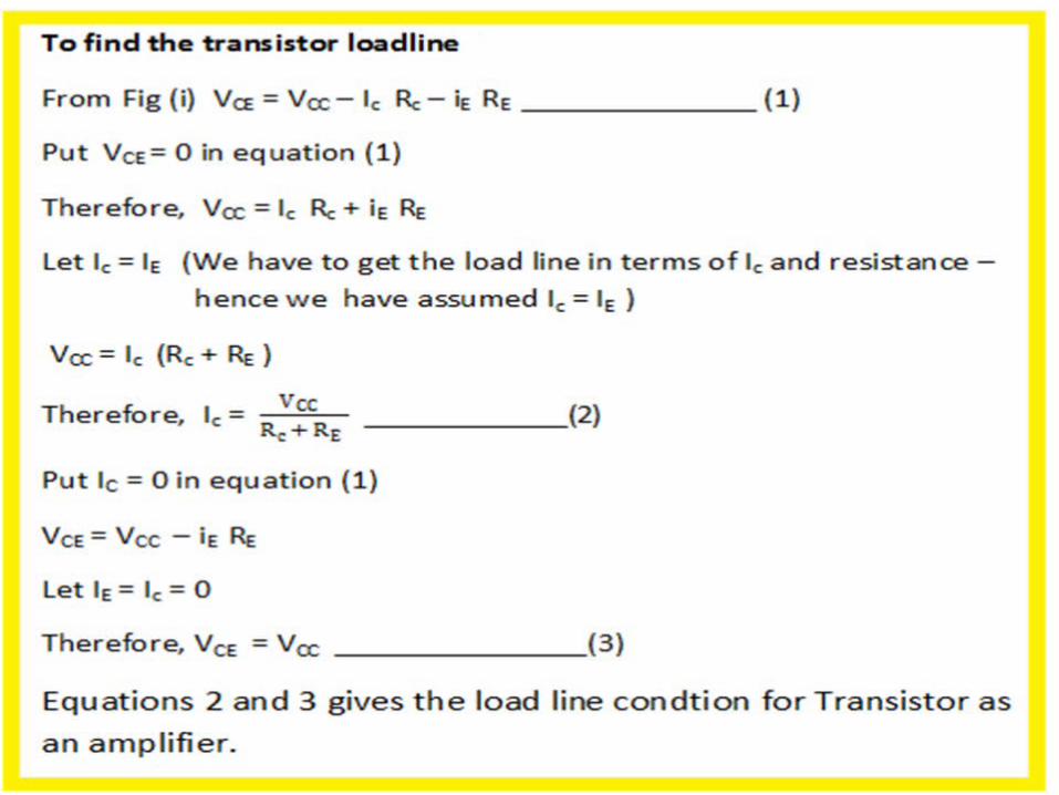
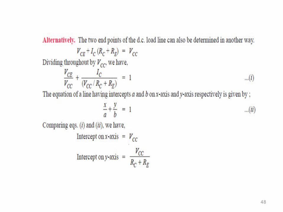
(i) d.c. load line. It is the line on the output characteristics of a transistor circuit which gives the values of IC and VCE corresponding to zero signal or d.c. conditions.
47
48
49
50
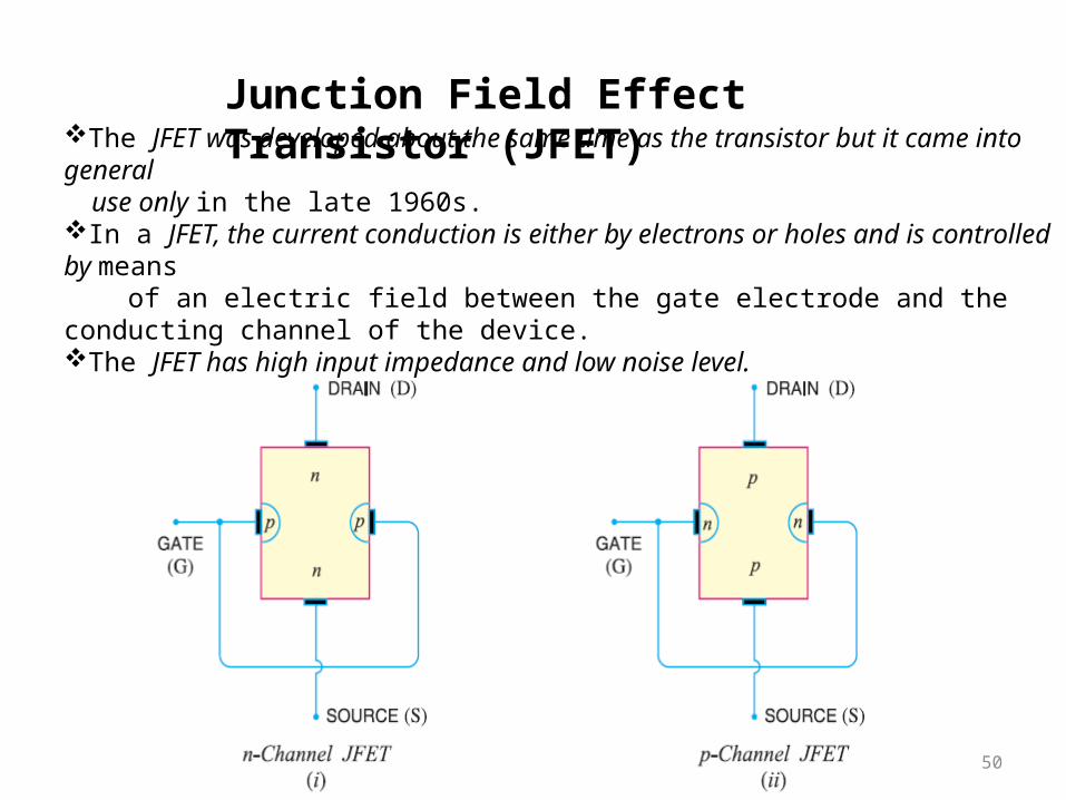
Junction Field Effect Transistor (JFET)The JFET was developed about the same time as the transistor but it came into general use only in the late 1960s. In a JFET, the current conduction is either by electrons or holes and is controlled by means of an electric field between the gate electrode and the conducting channel of the device. The JFET has high input impedance and low noise level.

51
52
53
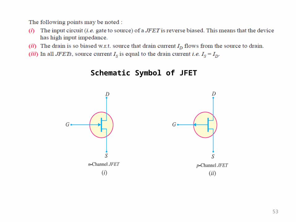
Schematic Symbol of JFET
54
It is clear from the above discussion that current from source to drain can becontrolled by the application of potential (i.e. electric field) on the gate. For thisreason, the device is called field effect transistor.
Note. If the reverse voltage VGS on the gate is continuously increased, a state isreached when the two depletion layers touch each other and the channel is cut off. Under such conditions, the channel becomes a nonconductor.
55
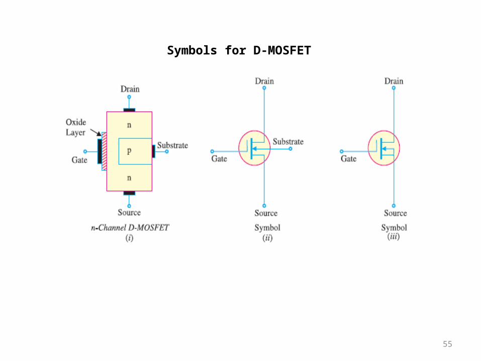
Symbols for D-MOSFET
56
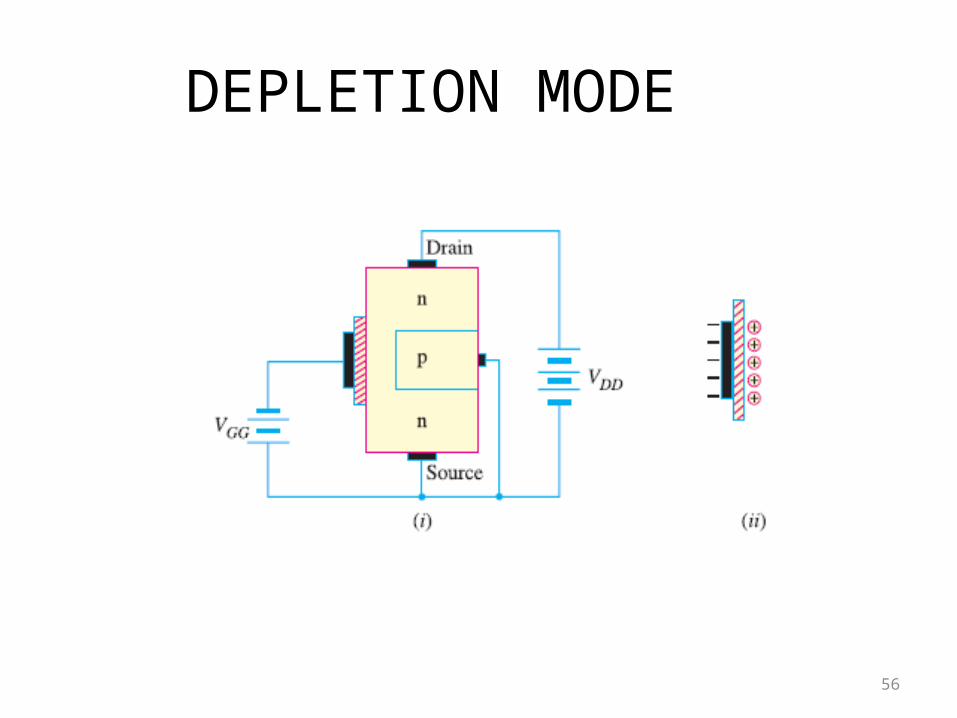
DEPLETION MODE
57
Circuit Operation of n channel D-MOSFET
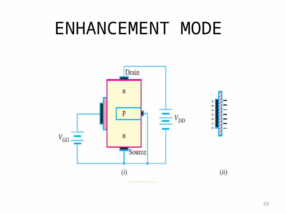
Fig. (i) shows the circuit of n-channel D-MOSFET. The gate forms a small capacitor. One plate of this capacitor is the gate and the other plate is the channel with metal oxide layer as the dielectric.When gate voltage is changed, the electric field of the capacitor changes which in turn changes the resistance of the n-channel. Since the gate is insulated from the channel, we can apply either negative or positive voltage to the gate. The negative-gate operation is called depletion mode whereas positive-gate operation is known as enhancement mode.
58
(i) Depletion mode. Fig.(i) shows depletion-mode operation of n- channel D-MOSFET. Since gate is negative, it means electrons are on the gate as shown is Fig. (ii). These electrons repel the free electrons in the n-channel, leaving a layer of positive ions in a part of the channel as shown in Fig. (ii). In other words, we have depleted (i.e. emptied) the n-channel of some of its free electrons. Therefore, lesser number of free electrons are made available for current conduction through the n-channel. This is the same thing as if the resistance of the channel is increased. The greater the negative voltage on the gate, the lesser is the current from source to drain. Thus by changing the negative voltage on the gate, we can vary the resistance of the n-channel and hence the current from source to drain. Note that with negative voltage to the gate, the action of D-MOSFET is similar to JFET. Because the action with negative gate depends upon depleting (i.e. emptying) the channel of free electrons, the negative-gate operation is called depletion mode.
59
ENHANCEMENT MODE
60
(ii) Enhancement mode. Fig. shows enhancement-mode operation of n-channel DMOSFET.Again, the gate acts like a capacitor. Since the gate is positive, it induces negative charges in the n-channel as shown in Fig. 19.48 (ii). These negative charges are the free electrons drawn into the channel. Because these free electrons are added to those already in the channel, the total number of free electrons in the channel is increased. Thus a positive gate voltage enhances or increases the conductivity of the channel. The greater the positive voltage on the gate, greater the conduction from source to drain.Thus by changing the positive voltage on the gate, we can change the conductivity of the channel.The main difference between D-MOSFET and JFET is that we can apply positive gate voltage to D-MOSFET and still have essentially *zero current. Because the action with a positive gate depends upon enhancing the conductivity of the channel, the positive gate operation is called enhancement mode.
61
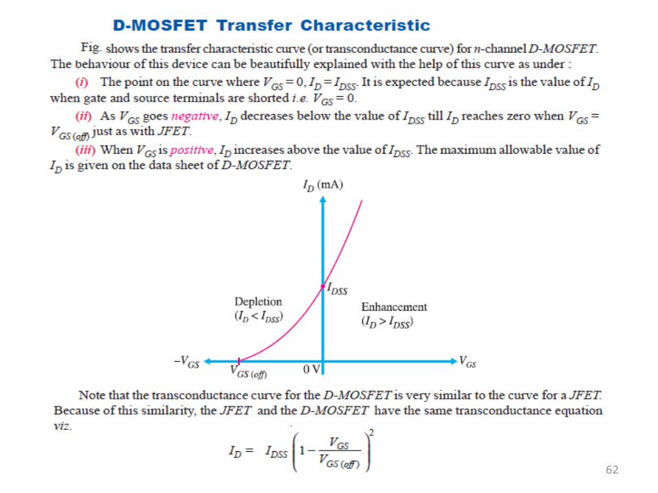
The following points may be noted about D-MOSFET operation :
(i) In a D-MOSFET, the source to drain current is controlled by the electric field of capacitor formed at the gate.(ii) The gate of JFET behaves as a reverse-biased diode whereas the gate of a D-MOSFET acts like a capacitor. For this reason, it is possible to operate D- MOSFET with positive or negative gate voltage.(iii) As the gate of D-MOSFET forms a capacitor, therefore, negligible gate current flows whether positive or negative voltage is applied to the gate. For this reason, the input impedance of D-MOSFET is very high, ranging from 10,000 MΩ to 10,000,00 MΩ.(iv) The extremely small dimensions of the oxide layer under the gate terminal result in a very low capacitance and the D-MOSFET has, therefore, a very low input capacitance. This characteristic makes the D- MOSFET useful in high-frequency applications.
62
63
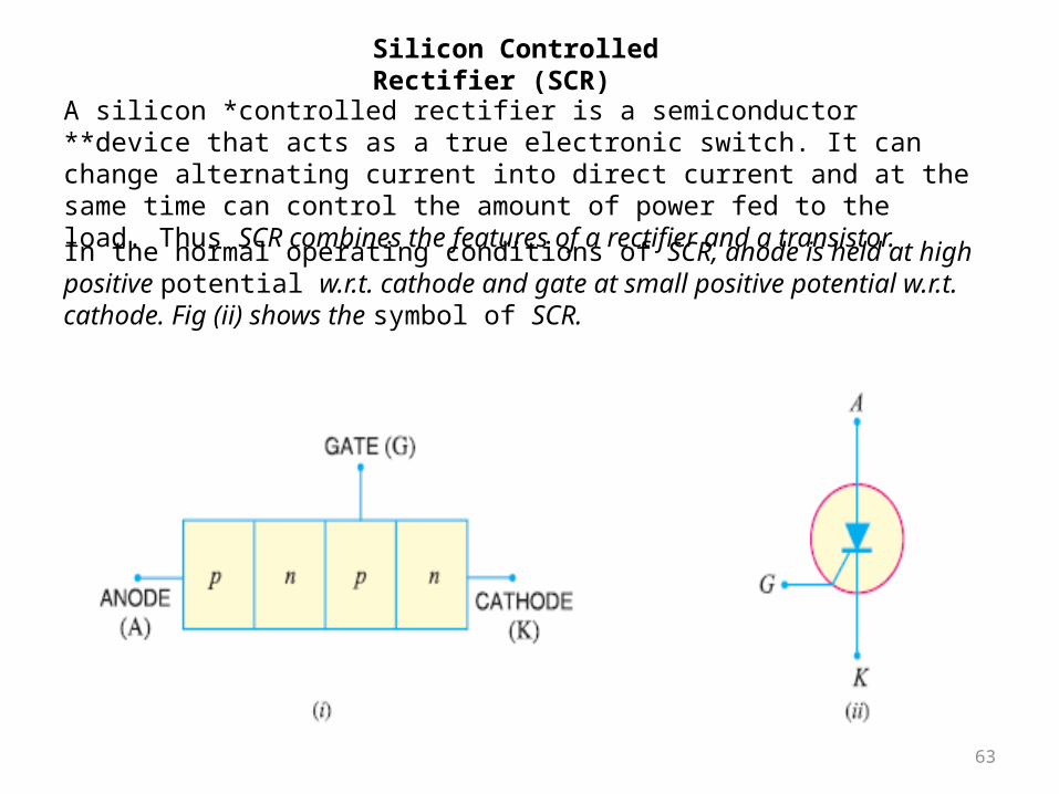
Silicon Controlled Rectifier (SCR)
A silicon *controlled rectifier is a semiconductor **device that acts as a true electronic switch. It can change alternating current into direct current and at the same time can control the amount of power fed to the load. Thus SCR combines the features of a rectifier and a transistor.
In the normal operating conditions of SCR, anode is held at high positive potential w.r.t. cathode and gate at small positive potential w.r.t. cathode. Fig (ii) shows the symbol of SCR.
64
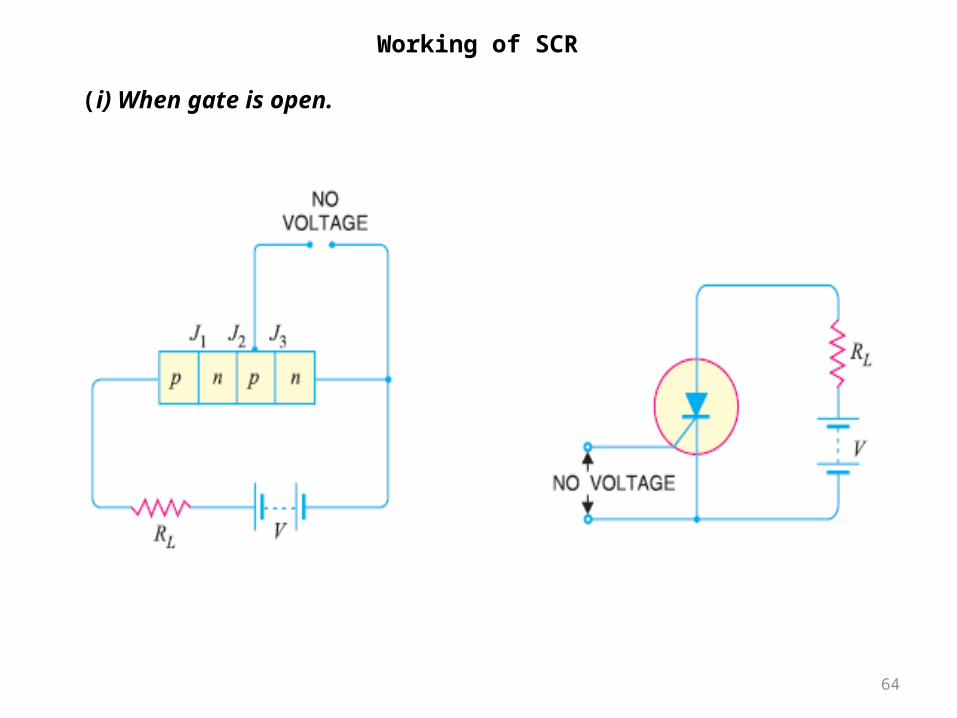
Working of SCR
(i) When gate is open.
65
Fig. shows the SCR circuit with gate open i.e. no voltage
applied to the gate. Under this condition, junction J2 is reverse biased while junctions J1 and J3 are forward biased. Hence, the situation in the junctions J1 and J3 is just as in a npn transistor with base open.Consequently, no current flows through the load RL and the SCR is cut off. However, if the applied voltage is gradually increased, a stage is reached when * reverse biased junction J2 breaks down. The SCR now conducts ** heavily and is said to be in the
ON state. The applied voltage at which SCR conducts heavily without gate voltage is called Breakover voltage.
66
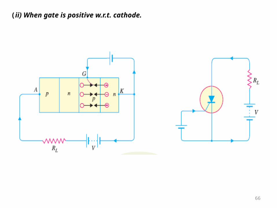
(ii) When gate is positive w.r.t. cathode.
67
The SCR can be made to conduct heavily at smaller applied voltage by applying a small positive potential to the gate as shown in Fig. Now junction J3 is forward biased and junction J2 is reverse biased. The electrons from n-type material start moving across junction J3 towards left whereas holes from p-type towards the right. Consequently, the electrons from junction J3 are attracted across junction J2 and gate current starts flowing. As soon as the gate current flows, anode current increases. The increased anode current in turn makes more electrons available at
junction J2. This process continues and in an extremely small time, junction J2 breaks down and the SCR starts conducting heavily. Once SCR starts conducting, the gate (the reason for this name is obvious) loses all control. Even if gate voltage is removed, the anode current does not decrease at all. The only way to stop conduction (i.e. bring SCR in off condition) is to reduce the applied voltage to zero.
68
Conclusion. The following conclusions are drawn from the working of SCR :(i) An SCR has two states i.e. either it does not conduct or it conducts
heavily. There is no state in between. Therefore, SCR behaves like a switch.
(ii) There are two ways to turn on the SCR. The first method is to keep the gate open and make the supply voltage equal to the breakover voltage. The second method is to operate SCR with supply voltage less than breakover voltage and then turn it on by means of a small voltage (typically 1.5 V, 30 mA) applied to the gate.
(iii) Applying small positive voltage to the gate is the normal way to close an SCR because the breakover voltage is usually much greater than supply voltage.
(iv) To open the SCR (i.e. to make it non-conducting ), reduce the supply voltage to zero.
69
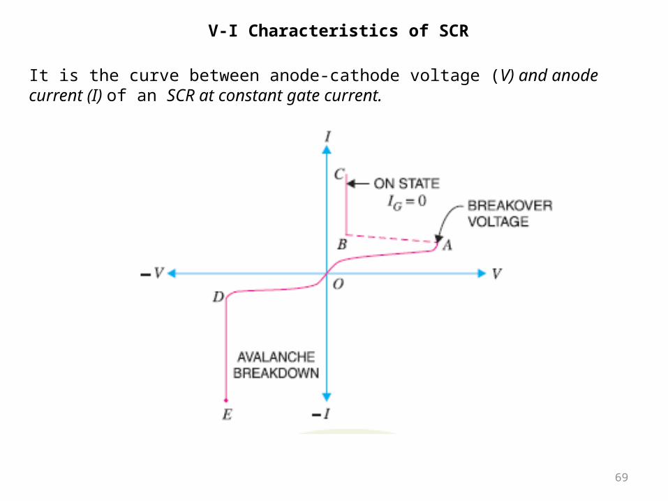
V-I Characteristics of SCR
It is the curve between anode-cathode voltage (V) and anode current (I) of an SCR at constant gate current.
70
(i) Forward characteristics. When anode is positive w.r.t. cathode, the curve
between V and I is called the forward characteristic. In Fig., OABC is the forward characteristic of SCR at
IG = 0. If the supply voltage is increased from zero, a point is reached (point A) when the SCR starts conducting.Under this condition, the voltage across SCR suddenly drops as shown by dotted curve AB and most of supply voltage appears across the load resistance RL. If proper gate current is made to flow, SCR can close at much smaller supply voltage.
71
(ii) Reverse characteristics. When anode is negative w.r.t. cathode, the curve between V
and I is known as reverse characteristic.
The reverse voltage does come across SCR when it is operated
with a.c. supply.
If the reverse voltage is gradually increased, at first the anode
current remains small (i.e.leakage current) and at some reverse voltage, avalanche breakdown occurs and the SCR starts conducting heavily in the reverse direction as shown by the curve DE.
This maximum reverse voltage at which SCR starts conducting
heavily is known as reverse breakdown voltage.
72
Unijunction Transistor (UJT)
A unijunction transistor (abbreviated as UJT) is a three-terminal semiconductor switching device.
This device has a unique characteristic that when it is triggered, the emitter current increases regeneratively until it is limited by emitter power supply.
Due to this characteristic, the unijunction transistor can be employed in a variety of applications e.g., switching, pulse generator, saw- tooth generator etc.
73
74
The following points are worth noting :
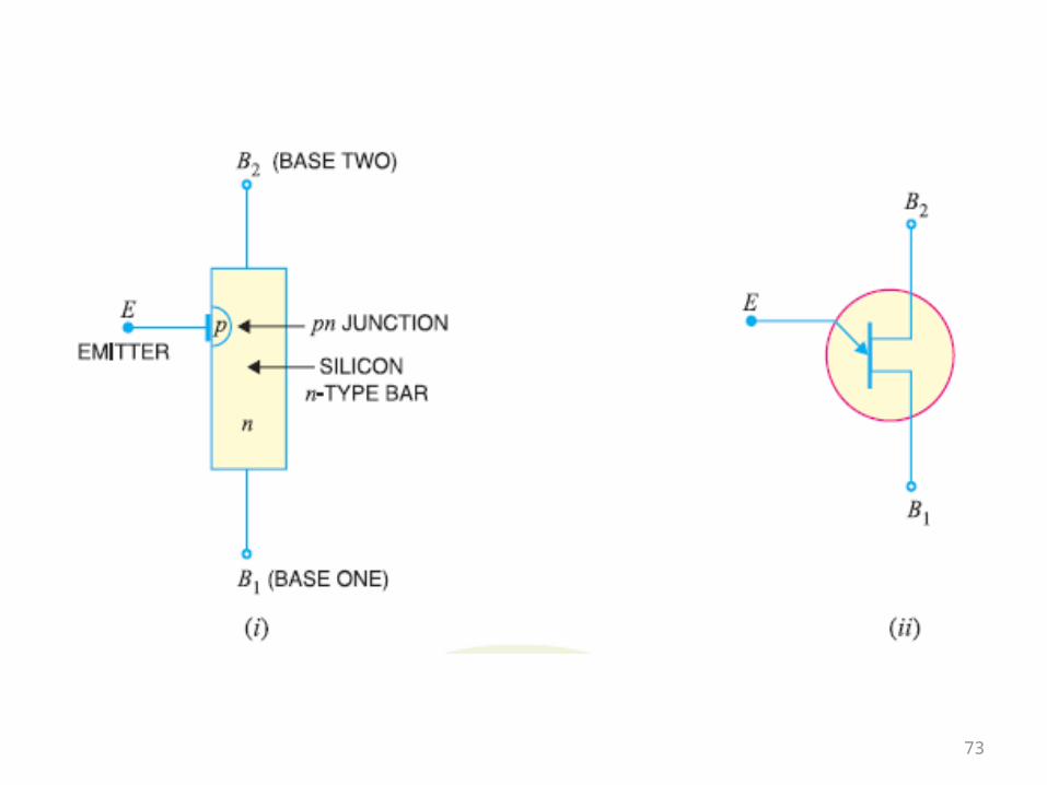
(i) Since the device has one pn junction and three leads, it is *commonly called a unijunction transistor (uni means
single).
(ii) With only one pn-junction, the device is really a form of diode. Because the two base terminals are taken from one section of the diode, this device is also called double- based diode.
(iii) The emitter is heavily doped having many holes. The n region, however, is lightly doped. For this reason, the resistance between the base terminals is very high ( 5 to 10 kΩ) when emitter lead is open.
75
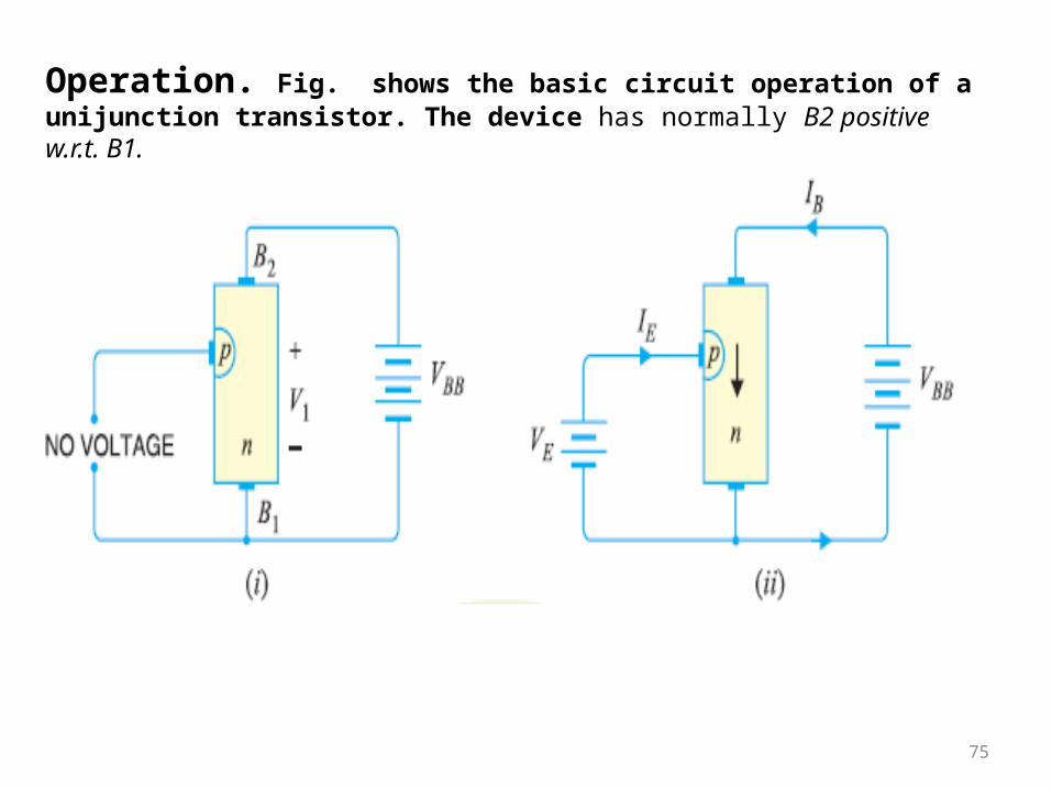
Operation. Fig. shows the basic circuit operation of a unijunction transistor. The device has normally B2 positive w.r.t. B1.
76
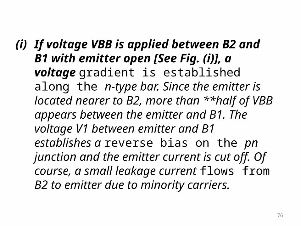
(i) If voltage VBB is applied between B2 and B1 with emitter open [See Fig. (i)], a voltage gradient is established along the n-type bar. Since the emitter is located nearer to B2, more than **half of VBB appears between the emitter and B1. The voltage V1 between emitter and B1 establishes a reverse bias on the pn junction and the emitter current is cut off. Of course, a small leakage current flows from B2 to emitter due to minority carriers.
77
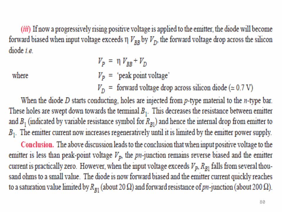
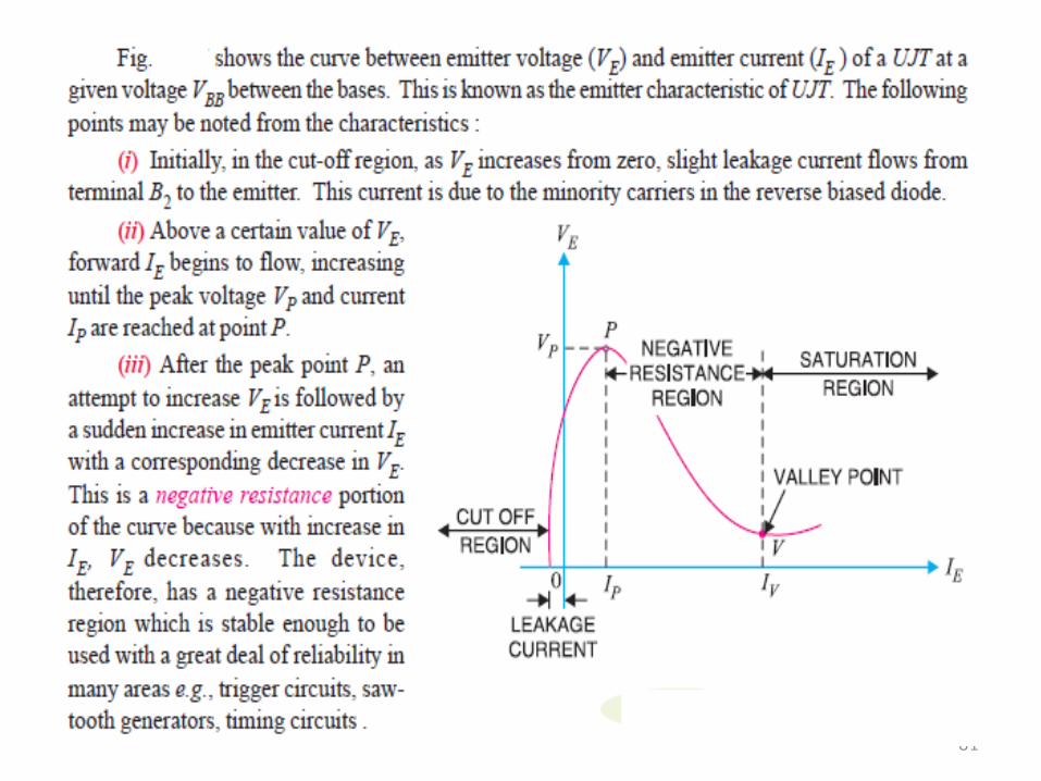
(ii) If a positive voltage is applied at the emitter [See Fig.(ii)], the pn junction will remain reverse biased so long as the input voltage is less than V1. If the input voltage to the emitter exceeds V1, the pn junction becomes forward biased. Under these conditions, holes are injected from p-type material into the n- type bar. These holes are repelled by positive B2 terminal and they are attractedtowards B1 terminal of the bar. This accumulation of holes in the emitter to B1 region results in the decrease of resistance in this section of the bar. The result is that internal voltage drop from emitter to B1 is decreased and hence the emitter current IE increases. As more holes are injected, a condition of saturation will eventually be reached. At this point, the emitter current is limited by emitter power supply only. The device is now in the ON state.(iii) If a negative pulse is applied to the emitter, the pn junction is reverse biased and the emittercurrent is cut off. The device is then said to be in the OFF state.
78
Equivalent Circuit of a UJT
79
80
81