Embed Size (px)
Citation preview
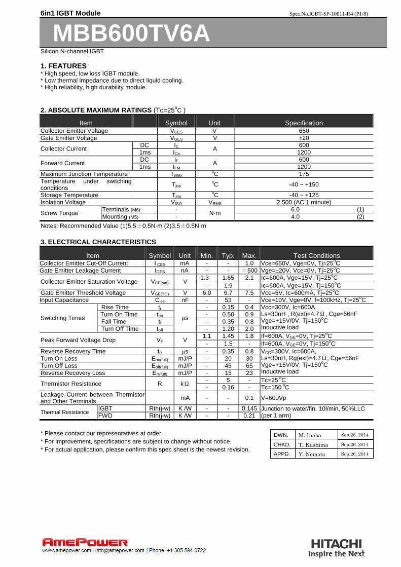
6in1 IGBT Module Spec.No.IGBT-SP-10011-R4 (P1/8)
MBB600TV6A
Silicon N-channel IGBT
1. FEATURES * High speed, low loss IGBT module. * Low thermal impedance due to direct liquid cooling. * High reliability, high durability module.
2. ABSOLUTE MAXIMUM RATINGS (Tc=25oC )
Item Symbol Unit Specification Collector Emitter Voltage VCES V 650
Gate Emitter Voltage VGES V 20
Collector Current DC IC
A 600
1ms ICp 1200
Forward Current DC IF
A 600
1ms IFM 1200
Maximum Junction Temperature Tjmax oC 175
Temperature under switching conditions
Tjop oC -40 ~ +150
Storage Temperature Tstg oC -40 ~ +125
Isolation Voltage VISO VRMS 2,500 (AC 1 minute)
Screw Torque Terminals (M6) -
N·m 6.0 (1)
Mounting (M5) - 4.0 (2)
Notes: Recommended Value (1)5.5±0.5N·m (2)3.5±0.5N·m
3. ELECTRICAL CHARACTERISTICS
Item Symbol Unit Min. Typ. Max. Test Conditions Collector Emitter Cut-Off Current I CES mA - - 1.0 Vce=650V, Vge=0V, Tj=25
oC
Gate Emitter Leakage Current IGES nA - - ±500 Vge=20V, Vce=0V, Tj=25oC
Collector Emitter Saturation Voltage VCE(sat) V 1.3 1.65 2.1 Ic=600A, Vge=15V, Tj=25
oC
- 1.9 - Ic=600A, Vge=15V, Tj=150oC
Gate Emitter Threshold Voltage VGE(TO) V 6.0 6.7 7.5 Vce=5V, Ic=600mA, Tj=25oC
Input Capacitance Cies nF - 53 - Vce=10V, Vge=0V, f=100kHz, Tj=25oC
Switching Times
Rise Time tr
s
- 0.15 0.4 Vcc=300V, Ic=600A Ls=30nH , R(ext)=4.7Ω, Cge=56nF Vge=+15V/0V, Tj=150
oC
Inductive load
Turn On Time ton - 0.50 0.9
Fall Time tf - 0.35 0.8
Turn Off Time toff - 1.20 2.0
Peak Forward Voltage Drop VF V 1.1 1.45 1.8 If=600A, VGE=0V, Tj=25
oC
- 1.5 - If=600A, VGE=0V, Tj=150oC
Reverse Recovery Time trr s - 0.35 0.8 VCC=300V, Ic=600A, Ls=30nH, Rg(ext)=4.7Ω, Cge=56nF Vge=+15V/0V, Tj=150
oC
Inductive load
Turn On Loss Eon(full) mJ/P - 20 30
Turn Off Loss Eoff(full) mJ/P - 45 65
Reverse Recovery Loss Err(full) mJ/P - 15 23
Thermistor Resistance R kΩ - 5 - Tc=25
oC
- 0.16 - Tc=150 o
C
Leakage Current between Thermistor and Other Terminals
mA - - 0.1 V=600Vp
Thermal Resistance IGBT Rth(j-w) K /W - - 0.145 Junction to water/fin, 10l/min, 50%LLC
(per 1 arm) FWD Rth(j-w) K /W - - 0.21
* Please contact our representatives at order.
* For improvement, specifications are subject to change without notice.
* For actual application, please confirm this spec sheet is the newest revision.
DWN.
CHKD.
M. Inaba Sep.26, 2014
T. Kushima
APPD. Y. Nemoto
Sep.26, 2014
Sep.26, 2014
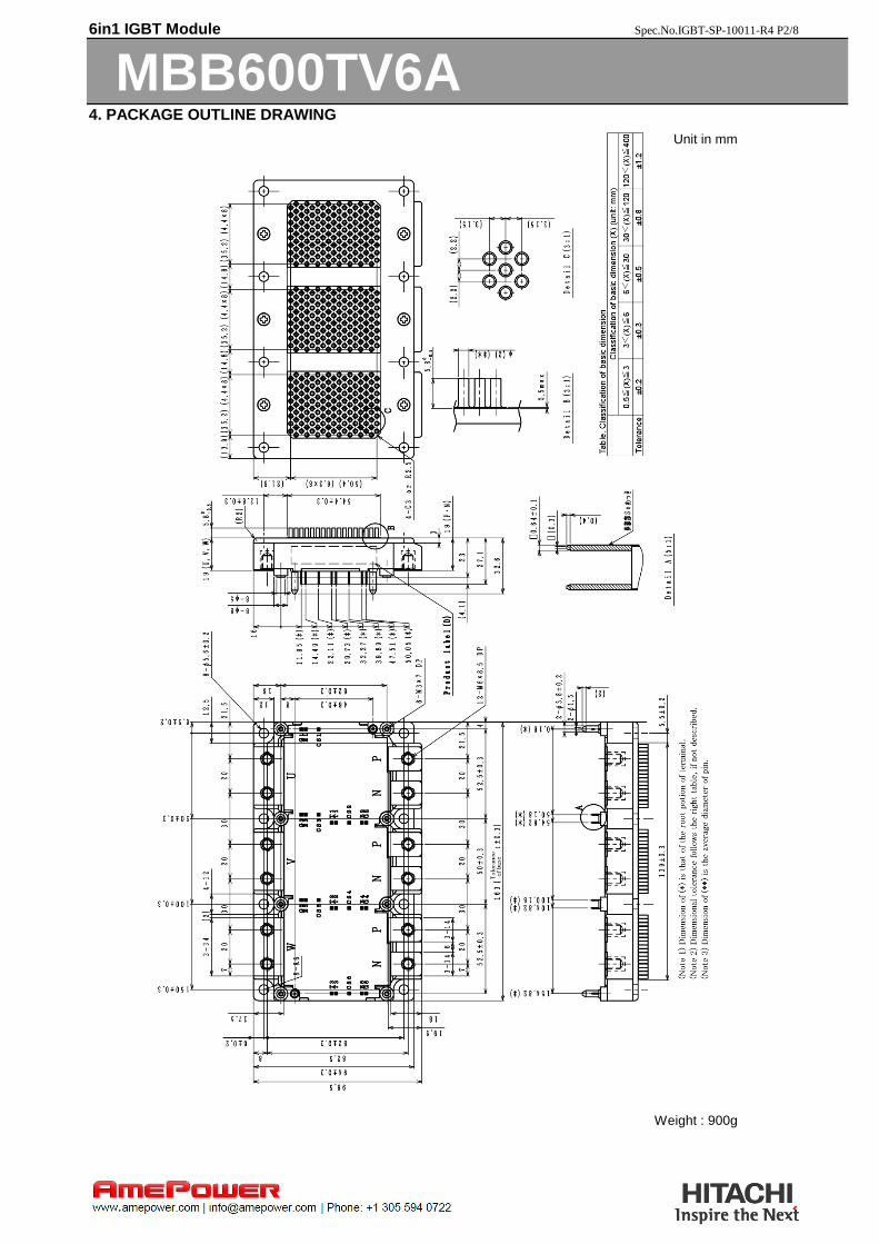
6in1 IGBT Module Spec.No.IGBT-SP-10011-R4 P2/8
MBB600TV6A
4. PACKAGE OUTLINE DRAWING
Weight : 900g
Unit in mm
6in1 IGBT Module Spec.No.IGBT-SP-10011-R4 (P3/8)
MBB600TV6A
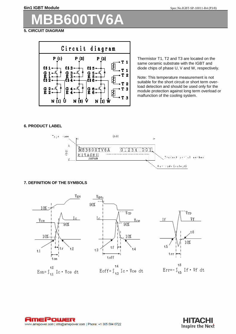
5. CIRCUIT DIAGRAM
6. PRODUCT LABEL
7. DEFINITION OF THE SYMBOLS
Thermistor T1, T2 and T3 are located on the
same ceramic substrate with the IGBT and
diode chips of phase U, V and W, respectively.
Note: This temperature measurement is not suitable for the short circuit or short term over-load detection and should be used only for the module protection against long term overload or malfunction of the cooling system.
6in1 IGBT Module Spec.No.IGBT-SP-10011-R4 (P4/8)
MBB600TV6A
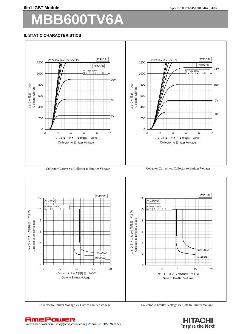
8. STATIC CHARACTERISTICS
Collector to Emitter Voltage vs. Gate to Emitter Voltage Collector to Emitter Voltage vs. Gate to Emitter Voltage
Collector Current vs. Collector to Emitter Voltage Collector Current vs. Collector to Emitter Voltage
コレ
クタ
電流
IC(A)
Collector to Emitter Voltage
コレクタ・エミッタ間電圧 VCE(V)
C
olle
cto
r C
urr
ent
TYPICAL
9V
10V
11V
VGE=15V14V13V12V
0
200
400
600
800
1000
1200
0 2 4 6 8 10
Tc=150℃
8V
Voltage sence:CS*-E*(*:1~6)
0
2
4
6
8
10
12
0 5 10 15 20
コレ
クタ
・エ
ミッ
タ間
電圧
VCE(V)
Gate to Emitter Voltage
ゲート・エミッタ間電圧 VGE(V)
C
olle
cto
r to
Em
itte
r V
oltage
TYPICAL
Tc=150℃
Ic=1200A
Ic=600A
Voltage sence:CS*-E*(*:1~6)
コレ
クタ
電流
IC(A)
Collector to Emitter Voltage
コレクタ・エミッタ間電圧 VCE(V)
Colle
cto
r C
urr
ent
TYPICAL
10V
VGE=15V14V13V12V11V
0
200
400
600
800
1000
1200
0 2 4 6 8 10
Tc=25℃
8V
9V
Voltage sence:CS*-E*(*:1~6)
0
2
4
6
8
10
12
0 5 10 15 20
コレクタ・エミッタ間電圧
VCE(V)
Gate to Emitter Voltage
ゲート・エミッタ間電圧 VGE(V)
Co
llecto
r to
Em
itte
r V
olta
ge
TYPICAL
Tc=25℃
Ic=1200A
Ic=600A
Voltage sence:CS*-E*(*:1~6)

6in1 IGBT Module Spec.No.IGBT-SP-10011-R4 (P5/8)
MBB600TV6A
9. DYNAMIC CHARACTERISTICS
TYPICAL
Sw
itch
ing
Tim
e
コレクタ電流 IC(A)
Collector Current
スイッチング時間
t (μ
S)
0
0.5
1
1.5
2
2.5
0 100 200 300 400 500 600 700
VCC=300VVGE=+15V/0V
Rgon/RGoff=4.7Ω
Cge=56nF
Tc=150℃
Ls≒30nH
Inductive Load
toff
tf
tr
ton
trr
Gate Charge Characteristics Forward Voltage of Free-Wheeling Diode
ゲート・エミッタ間電圧 VGE(V)
ゲート電荷 QG(nC)
Gate Charge
Ga
te t
o E
mitte
r V
olta
ge
TYPICAL
0
5
10
15
20
Vcc=300V
Ic=600A
Tc=25℃
0 20001000
Switching Time vs. Collector Current Switching Time vs. Gate Resistance
Fo
rwa
rd C
urr
en
t
順電圧 VF(V)
Forward Voltage順電流 IF(A)
TYPICAL
0
200
400
600
800
1000
1200
0 1 2 3 4 5
VGE=0
Tc=25℃Tc=150℃
Voltage sence:CS*-E*(*:1~6)
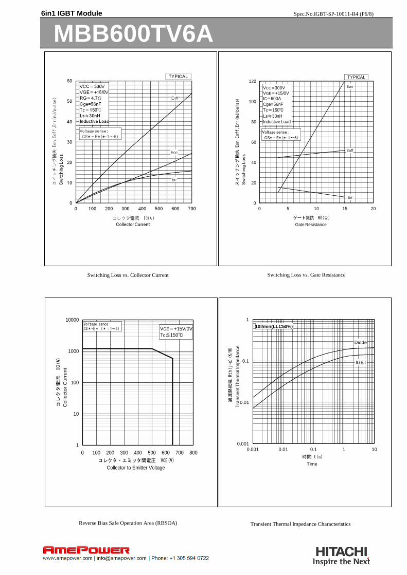
6in1 IGBT Module Spec.No.IGBT-SP-10011-R4 (P6/8)
MBB600TV6A
0
20
40
60
80
100
120
0 5 10 15 20
Sw
itch
ing
Lo
ss
ゲート抵抗 RG(Ω)
Gate Resistance
スイ
ッチン
グ損失
Eon,Eoff,Err(mJ/pulse)
TYPICAL
VCC=300VVGE=+15/0VIC=600A
Cge=56nF
Tc=150℃
Ls≒30nH
Inductive Load
Eoff
Eon
Err
Voltage sense;
CS* - E* (*:1~6)
0.001
0.01
0.1
1
0.001 0.01 0.1 1 10
Tra
nsie
nt T
he
rmal I
mp
ed
ance
時間 t(s)
Time
過渡熱抵抗
Rth(j-c)(K/W)
Diode
IGBT
10l/min(LLC50%)
Reverse Bias Safe Operation Area (RBSOA)
Switching Loss vs. Collector Current Switching Loss vs. Gate Resistance
Transient Thermal Impedance Characteristics
Co
lle
cto
r C
urr
en
t
コレクタ・エミッタ間電圧 VCE(V)
Collector to Emitter Voltage
コレクタ電流 IC(A)
1
10
100
1000
10000
0 100 200 300 400 500 600 700 800
VGE=+15V/0V
Tc≦150℃
Voltage sence:CS*-E*(*:1~6)

6in1 IGBT Module Spec.No.IGBT-SP-10011-R4 (P7/8)
MBB600TV6A
0
200
400
600
800
1000
1200
1400
1600
0 100 200 300 400 500 600 700 800
Co
llecto
r C
urr
en
t (F
orw
ard
Cu
rre
nt)
コレクタ・エミッタ間電圧 VCE(V)
Collector to Emitter Voltage
コレ
クタ
電流
-IC(=IF) (A)
VGE=+15/0VTc≦150℃
Voltage sense:
CS* - E* (*:1~6)
10. THERMISTOR
Reverse Recovery Safe Operation Area (RRSOA)
Resistance vs. Temperature
0.1
1
10
020406080100120
抵抗
値(k
Ω)
温度 (℃)
For reference(Data from manufacturer)
Temperature
Resis
tance
Table1 Specifications of Thermistor(For reference)
Nominal zero-power resistance 5kΩ ±3%(25℃)
B value 3375K±2%(25~50℃)
Operating temperature range ‐50~150℃
Thermal time constant(in still air) Approx. 10 sec.

6in1 IGBT Module Spec.No.IGBT-SP-10011-R4 (P8/8)
MBB600TV6A
HITACHI POWER SEMICONDUCTORS
For inquiries relating to the products, please contact nearest overseas representatives that is located
“Inquiry” portion on the top page of a home page.
Hitachi power semiconductor home page address http://www.hitachi-power-semiconductor-device.co.jp/en/
Notices
1. The information given herein, including the specifications and dimensions, is subject to
change without prior notice to improve product characteristics. Before ordering,
purchasers are advised to contact Hitachi sales department for the latest version of this
data sheets.
2. Please be sure to read "Precautions for Safe Use and Notices" in the individual brochure
before use.
3. In cases where extremely high reliability is required (such as use in nuclear power
control, aerospace and aviation, traffic equipment, life-support-related medical
equipment, fuel control equipment and various kinds of safety equipment), safety should
be ensured by using semiconductor devices that feature assured safety or by means of
users’ fail-safe precautions or other arrangement. Or consult Hitachi’s sales department
staff.
4. In no event shall Hitachi be liable for any damages that may result from an accident or
any other cause during operation of the user’s units according to this data sheets. Hitachi
assumes no responsibility for any intellectual property claims or any other problems that
may result from applications of information, products or circuits described in this data
sheets.
5. In no event shall Hitachi be liable for any failure in a semiconductor device or any
secondary damage resulting from use at a value exceeding the absolute maximum rating.
6. No license is granted by this data sheets under any patents or other rights of any third
party or Hitachi Power Semiconductor Device, Ltd.
7. This data sheets may not be reproduced or duplicated, in any form, in whole or in part,
without the expressed written permission of Hitachi Power Semiconductor Device, Ltd.
8. The products (technologies) described in this data sheets are not to be provided to any
party whose purpose in their application will hinder maintenance of international peace
and safety not are they to be applied to that purpose by their direct purchasers or any
third party. When exporting these products (technologies), the necessary procedures are
to be taken in accordance with related laws and regulations.


![Data-sheet electronic braking system VersiBrake [40 - 600A] · Elektronic Braking System VB [40 — 600A] Electronic Braking System VersiBrake [40 - 600A] Typical Applications: ventilators](https://img.pdfslide.net/doc/110x75/5e156b092a3f3c6e3c58bd78/data-sheet-electronic-braking-system-versibrake-40-600a-elektronic-braking-system.jpg)