Embed Size (px)
Citation preview

http://www.graphene.manchester.ac.uk
Graphene and 2D-material optoelectronics
Tim Echtermeyer School of Electrical and Electronic Engineering
University of Manchester UK
Tel: +44 (0)161 275 1932

Outline
• Introduction
• Modulation
• Detection
• Optoelectronics @UoM/NGI
• Conclusions

Introduction
NGI
School of EEE
Photon Science Institute

Introduction
Optoelectronics…
… is a wide field
Mainly:
electrical-to-optical or
optical-to-electrical transduction
Encompasses three main areas:
• Generation F. Withers (15:00)
• Modulation
• Detection

Introduction
Why graphene and 2D-materials?
• Large spectral range
• High speed
• Can be integrated into CMOS-BEOL
• Thin flexible electronics, coatings
• Combinable with other materials, e.g. plasmonics, nanoparticles,…
• Extended functionality, e.g. optoelectronic sensing

Modulation

Modulation
Graphene/hBN based modulator
B.D. Thackray et. al., Nano Lett.. 15, 3519 (2015).

Detection

Detection
A bit of history… - First observation
Lee et. al., Nature Nanotechnol. 3, 486 (2008).

Detection
A bit of history… - First observation Metal-induced doping
Giovanetti et. al., Phys. Rev. Lett. 101, 026803 (2008).
e-h pair creation
Metal
e-h separation

Detection
Near-field
Mueller et. al., Phys. Rev. B. 79, 245430 (2009).
Near-field scanning optical microscope
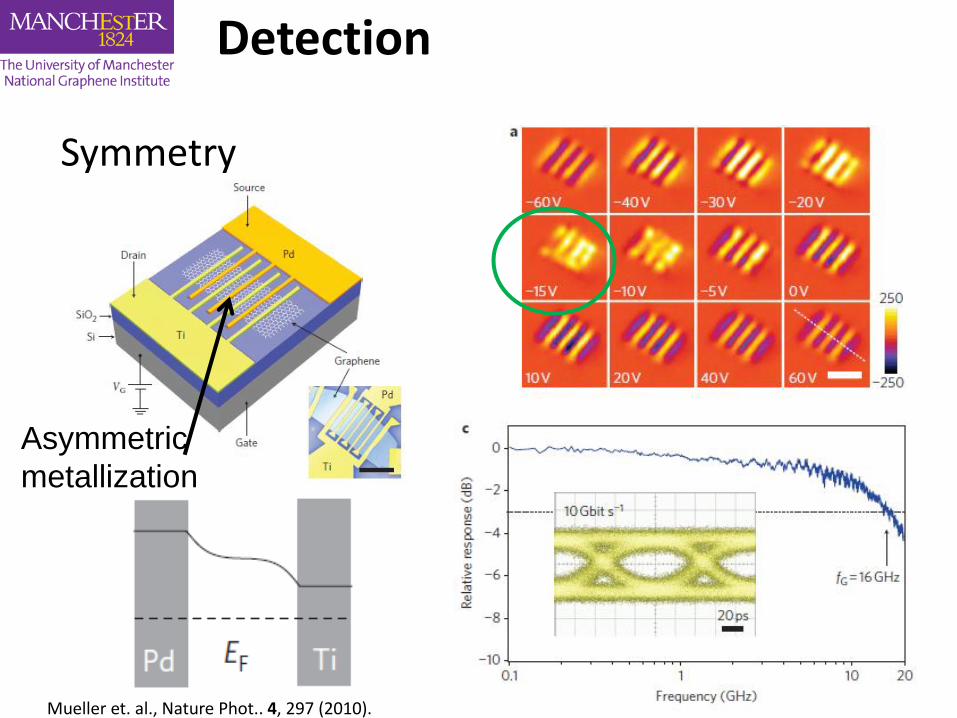
Detection
Symmetry
Mueller et. al., Nature Phot.. 4, 297 (2010).
Asymmetric
metallization

Detection
A bit of history…
M.C. Lemme, F.H.L. Koppens, et. al, Nano Lett. 11, 4134 (2011) N.M. Gabor et. al., Science 4, 648 (2011).
Photo-thermo-electric effect
Song et. al., Nano Lett. 11, 468 (2011).
Dual-gated
FET on hBN

Detection
Plasmonic Enhancement
T.J. Echtermeyer et. al., Nat. Commun. 2, 458 (2011).

Detection
Plasmonic Enhancement
T.J. Echtermeyer et. al., Nat. Commun. 2, 458 (2011).

Detection
Plasmonic Enhancement
T.J. Echtermeyer et. al., Nat. Commun. 2, 458 (2011).

Detection
Combination with QD
G. Konstantatos et. al., Nat. Nano. 7, 363 (2011)

Detection
Bolometric detection of THz radiation
X. Cai et. al., Nat. Nano. 9, 814 (2014)

Detection
THz detection through plasma-waves
Vicarelli, L. et al. Nature Mater. 11, 865 (2012)

Detection
Intrinsic graphene plasmons
M. Freitag et. al., Nat. Communications 4, 1951 (2013)
λ = 10.6μm

Detection
Mechanisms
F. Koppens et. al., Nat. Nano. 9, 780 (2014)

Detection
Mechanisms
UV VIS NIR, SWIR | | | | THz | FIR MIR | LWIR

Detection
Spectral range
UV VIS NIR, SWIR | | | | THz | FIR MIR | LWIR
Graphene MGM
Graphene Waveguide
Graphene QDs
Graphene Plasmonics
Graphene Plasma waves
Graphene Intrinsic Plasmons
Graphene Bolometric
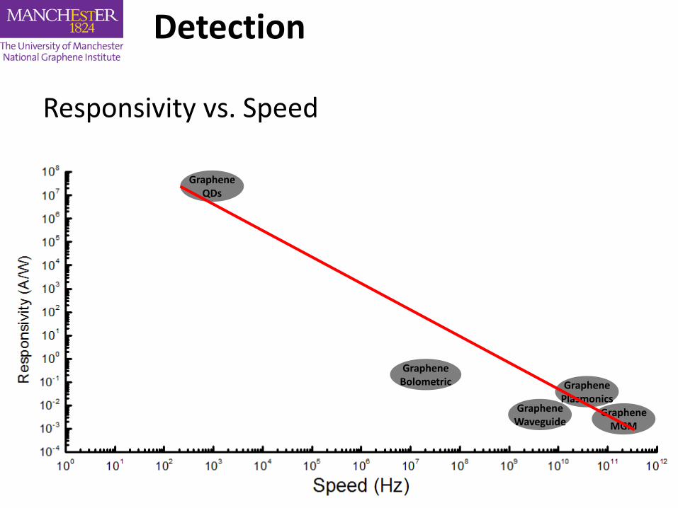
Detection
Responsivity vs. Speed
Graphene MGM
Graphene Waveguide
Graphene QDs
Graphene Plasmonics
Graphene Bolometric

Detection
A wide spectrum of potential applications
(Band gap)
Graphene
UV VIS NIR, SWIR | | | | THz | FIR MIR | LWIR
MoS2
Phosphorene Black Phos.
Si
Ge
InGaAs

Optoelectronics @ UoM/NGI

Optoelectronics @ UoM/NGI
Work in a variety of fields:
• Light emission
• Graphene/2D material based heterostructures
• THz lasers
• Modulation
• Plasmonic-Graphene/2D material based modulators
• Photodetection
• Graphene/2D material based
• Combination with plasmonics

Optoelectronics @ UoM/NGI
Work enabled through
• State-of-the art clean room facilities and labs
• Optical characterisation
• Raman, PL
• Ellipsometry
• Microphotospectrometer
• Electro-optical characterisation
• Scanning photocurrent microscopy
• DC – measurements under full illumination

Conclusions
• High versatility of graphene/2D-materials for
applications in different wavelength ranges • No “one-fits all” approach
• Ultra-high intrinsic speed possible
• Diverse work carried out at the NGI in all the fields of optoelectronics: emission, modulation, detection
• State-of-the art facilities @NGI for optoelectronics